Embed Size (px)
Citation preview
Oversampling A/D Converters with Improved Signal Transfer Functions
© Copyright by Bupesh Pandita (2010)
by
A thesis submitted in conformity with the requirements
for the degree of Doctor of Philosphy
Graduate Department of Electrical and Computer Engineering
University of Toronto
Bupesh Pandita
Oversampling A/D Converters with Improved Signal Transfer Functions
Bupesh Pandita
Doctor of Philosophy
Department of Electrical and Computer Engineering
University of Toronto
2010
Abstract
This thesis proposes a low-IF receiver architecture suitable for the realization of single-
chip receivers. To alleviate the image-rejection requirements of the front-end filters an
oversampling complex discrete-time ΔΣ ADC with a signal-transfer function that achieves
a significant filtering of interfering signals is proposed. A filtering ADC reduces the com-
plexity of the receiver by minimizing the requirements of analog filters in the IF digitiza-
tion path. Discrete-time ΔΣ ADCs have precise resonant frequency and clock frequency
ratios and, hence, do not require the calibration or tuning that is necessary in the case of
continuous-time ΔΣ modulator implementations. This feature makes the proposed dis-
crete-time ΔΣ ADC ideal for multistandard receiver applications.
The ΔΣ modulator signal-transfer function (STF) and noise-transfer function (NTF)
have been designed using complex filter routines based on classical filter design proce-
dures. With a filtering STF and stop band attenuation greater than 30dB, the ΔΣ modulator
reduces intermodulation of the desired signal and the interfering signals at the input of the
ii
quantizer, and also avoids feedback of the high-frequency interfering signals at the input
of the modulator.
The reported complex ΔΣ ADC is intended for DTV receiver applications. With a max-
imum intended sampling frequency of 128 MHz and an OSR of 16, the ADC has been
designed to support a maximum DTV signal bandwidth of 8 MHz. Except for a somewhat
reduced maximum sampling frequency, the test results of the prototype complex ΔΣ mod-
ulator are very close to the simulated results. The IC achieved 70.9 dB SNDR over a 6
MHz band centered around 3 MHz. The image rejection ratio (IRR) of the ΔΣ ADC was
measured to be greater than 65d B. The measurement results confirm the filtering charac-
teristics of the ADC. The fabricated chip consumes 177 mW and occupies a silicon area of
2.15 mm2.
iii

Acknowledgments
I would like to thank my thesis supervisor Professor Ken Martin for his guidance and
technical expertise. Professor Martin’s deep insight, experience, and incisive feedback
helped me to stay focussed and complete the thesis.
To Professor David Johns for critically reviewing some of the sections of the thesis.
The review forced me to revisit some of my assumptions and in the process brought out
some of the main contributions of this thesis.
I would like to thank Professor Dimitrios Hatzinakos, Professor Chan Carusone, and
Professor Ali Sheikholeslami for agreeing to be on the final oral examination commitee.
Professor Ali Sheikholeslami and Professor Chan Carussone pointed out some of the mis-
takes which will save me some of the blushes in future. Thanks to Professor David Nairn
for agreeing to be the external examiner and also for his inputs and comments.
Thanks to all friends at the ECE department- Faisal Musa for guiding me when I was
new to the University, Mohammed Abdallah, M. Hossain, Alireza for his technical discus-
sions, Kentaro for getting me started with the layout, Rituraj for his discussions on CMOS
circuits and philosphy in life.
I would also like to take this opportunity to thank Muthu Krishnanan Chinnasamy for
motivating me to embark upon this PhD journey.
I would like to thank my parents for always ecouraging me to give my best and not to
worry too much about the results.
iv

Finally, I would like to express my deepest gratitude to my wife, Jyotika, and daughter,
Avantika, who stood by me through all these years of studentship.
v
Table of Contents
Chapter 1 Introduction .....................................................................................................1
1.1 Motivation and Background ....................................................................................1
1.2 Digital TV (DTV) Receivers ...................................................................................5
1.3 Thesis Outline ..........................................................................................................9Chapter 2 A Low-IF Complex ΔΣ ADC-based DTV Receiver ....................................13
2.1 Background............................................................................................................142.1.1 Real Mixing versus Complex Mixing ...............................................................................142.1.2 Complex Filters .................................................................................................................152.1.3 Mismatch in Complex Filters ............................................................................................16
2.2 A Low-IF DTV Receiver Architecture ..................................................................17
2.3 The ‘Interfering Signals’ Problem in Wireless Receivers .....................................20
2.4 Approaches to Filtering Interfering Signals in ΔΣ ADC based Receivers ............222.4.1 Filtering Interfering Signals in the Digital Domain...........................................................222.4.2 Filtering Interfering Signals in the Analog Domain ..........................................................232.4.3 Filtering Interfering Signals with a Filtering STF .............................................................23
2.5 Specifications for a Complex ΔΣ ADC Used in a DTV Receiver .........................292.5.1 Mismatch and Image Rejection Requirements of the Low-IF Complex ΔΣ ADC...........33
Chapter 3 A Complex ΔΣ Modulator with an Improved STF.....................................38
3.1 ΔΣ Modulator Transfer Functions..........................................................................39
3.2 NTF-STF Design Trade-Off ..................................................................................41
3.3 Background............................................................................................................473.3.1 The Norm and its Impact on the NTF Poles .....................................................................473.3.2 The Loss Function L(Z).....................................................................................................50
3.4 STF-NTF Co-Design Optimization Algorithm for the Design of Real ΔΣ Modulators53
3.5 Power and Performance Analysis of the Proposed Real ΔΣ Modulator ................573.5.1 Background- SIMULINK Model for SC Integrators with Finite Opamp DC Gains ........623.5.2 Power Comparison ............................................................................................................633.5.3 Sensitivity to Intermodulation due to DAC Non-linearity ................................................653.5.4 Stability Comparison .........................................................................................................72
3.6 The STF-NTF Co-Design Optimization Algorithm for the Design of Complex ΔΣ Modulators72
3.7 Power and Performance Analysis of the Proposed Complex ΔΣ Modulator.........853.7.1 ΔΣ modulator with Unity STF..........................................................................................853.7.2 Power Comparison ...........................................................................................................883.7.3 Sensitivity to Intermodulation due to DAC Non-linearity ................................................913.7.4 Comparison with a Discrete-Time Receiver [14][15] .......................................................98
vi
3.7.5 Comparison with an SC + FeedForward ADC with Unity STF......................................100
3.8 Advantages of the proposed ΔΣ Modulator architecture .....................................106Chapter 4 Architectural-Level Design of the Experimental ΔΣ Modulator.............111
4.1 Background..........................................................................................................111
4.2 Mismatches in a Complex ΔΣ Modulator ............................................................1134.2.1 An Improved Complex ΔΣ Modulator ...........................................................................121
4.3 The Switched-Capacitor Architecture .................................................................1274.3.1 Complex Integrators ........................................................................................................1274.3.2 Dynamic Range Scaling ..................................................................................................1274.3.3 Multibit Quantization ......................................................................................................1274.3.4 Multilevel DAC ...............................................................................................................1284.3.5 Realizing the Feedins.......................................................................................................1284.3.6 The Complete Fully-Differential SC Architecture ..........................................................1294.3.7 The Clocking Scheme......................................................................................................131
4.4 System-level Behavioral Simulations ..................................................................1324.4.1 Capacitor Sizing ..............................................................................................................132
4.4.1.1 Capacitor Mismatch ..........................................................................................1324.4.1.2 Noise Analysis...................................................................................................133
4.4.2 Clock-Jitter ......................................................................................................................1474.4.3 Opamp Nonidealities .......................................................................................................147
4.4.3.1 Opamp Finite DC Gain .....................................................................................1474.4.3.2 Unity-Gain Frequency and Slew Rate...............................................................149
4.4.4 Switch On-Resistances ....................................................................................................151Chapter 5 Integrated Circuit Implementation............................................................154
5.1 The Complete Fourth-Order SC-Modulator ........................................................154
5.2 Clock Generator ...................................................................................................156
5.3 Sampling Switches...............................................................................................158
5.4 Operational Amplifier..........................................................................................1595.4.1 Main Stage .......................................................................................................................1595.4.2 Bias Stage ........................................................................................................................1615.4.3 Gain-Boosting Amplifiers ...............................................................................................1645.4.4 Device Sizes ....................................................................................................................1655.4.5 SC CMFB Circuit ............................................................................................................168
5.5 Quantizers ............................................................................................................1695.5.1 Comparator ......................................................................................................................1695.5.2 Resistor Ladder................................................................................................................173
5.6 Layout ..................................................................................................................1735.6.1 Capacitor..........................................................................................................................1755.6.2 Switches...........................................................................................................................1765.6.3 Comparators.....................................................................................................................1775.6.4 Amplifiers ........................................................................................................................1785.6.5 The Resistor Ladder.........................................................................................................179
vii
5.7 Substrate and Supply Noise Decoupling .............................................................180Chapter 6 Testing and Experimental Results .............................................................182
6.1 The Integrated Circuit ..........................................................................................1826.1.1 Pins ..................................................................................................................................183
6.2 The Test Set-Up ...................................................................................................185
6.3 The PCB Design ..................................................................................................189
6.4 Test Results ..........................................................................................................191
6.5 Performance Summary ........................................................................................196
6.6 Explaining the Differences between the Measured and the Simulated Results...1986.6.1 Instability and SNDR Degradation with Higher Frequencies .........................................1986.6.2 Difference Between the Measured and the Desired STF.................................................202
6.7 Power Dissipation ................................................................................................205Chapter 7 Conclusions...................................................................................................210
7.1 Contributions .......................................................................................................210
7.2 Suggestions for Future Work ...............................................................................2127.2.1 Continuous-time Modulator Architectures ......................................................................2127.2.2 Frequency-Translating Complex ΔΣ Modulator..............................................................2127.2.3 Demodulator Architectures..............................................................................................212
viii
List of Figures
Figure 1.1 DTV receiver front-end block diagram ............................................. 5Figure 1.2 Single-conversion DTV receiver block diagram example................ 6Figure 1.3 Double-conversion DTV receiver block diagram example ............... 6Figure 1.4 Double-conversion DTV receiver block diagram [2] ........................ 8Figure 1.5 Single-conversion DTV receiver architecture[8]............................... 9Figure 2.1 Mixing a real signal with a sinusoid: (a) mixer input spectra, (b) mixer
output spectrum................................................................................ 14Figure 2.2 Realizing a complex filter with real filter blocks. ........................... 16Figure 2.3 a) Complex filter constructed from non-ideal components, and b)
Signal flow diagram of a complex filter A(z), showing common-mode and differential error components. ................................................... 17
Figure 2.4 A quadrature-IF system using a complex Low-IF ΔΣ modulator. ... 18Figure 2.5 (a) ΔΣ modulator with distributed feedforward summation, (b) ΔΣ
modulator with distributed feedback. (c) Modified distributed feedforward ΔΣ modulator with feed-ins to introduce STF zeros. .. 24
Figure 2.6 NTFs and STFs for the ΔΣ modulators with distributed feedforward and distributed feedback: (a) ΝΤΦ, (b) STF. ................................... 26
Figure 2.7 (a) Modified feedback ΔΣ modulator [12], (b) STFs for the modulator architectures ..................................................................................... 27
Figure 2.8 ΔΣ modulator with additional low pass and high pass filters in forward and feedback paths to implement a filtering STF [13]. ................... 28
Figure 2.9 ΔΣ modulator with a notch in the stopband to implement a filtering STF [14]. .......................................................................................... 29
Figure 2.10 The interfering signals for DVB-T with a third order complex bandpass filter at the input of the ΔΣ ADC...................................... 31
Figure 2.11 A complex ΔΣ modulator structure with mismatch in gain elements.. 34
Figure 3.1 A complex ΔΣ modulator structure.................................................. 39Figure 3.2 Structure for the proposed fourth-order ΔΣ modulator with input feed-
ins to realize zeros in the STF. ......................................................... 40Figure 3.3 Effect of ε on the attenuation characteristics of a filter ................... 42Figure 3.4 Plot of the magnitude of the fourth-order Chebyshev filter for different
values of the stop-band attenuation parameter L ............................. 45Figure 3.5 Movement of the poles of H(s) for increasing values of the attenuation
parameter L ...................................................................................... 46Figure 3.6 Root-locus of the equation (3.8) as the filter attenuation, L, varies. 47Figure 3.7 (a) NTF magnitude for different values of the |L|1 norm, (b)
movement of the NTF poles with an increase in the |L|1 norm....... 49Figure 3.8 A flow chart for filter designing with defined stop-band zeros and
passband response type [4] .............................................................. 51
ix
Figure 3.9 Real Transfer functions for SQNR=88 dB. (a) NTF magnitude response, (b) pole-zero constellation for the non-optimized NTF, (c) pole-zero constellation for the optimized NTF, d) STF magnitude response, (e) pole-zero constellation for the non-optimized STF, (f) pole-zero constellation for the optimized STF ................................ 54
Figure 3.10 Real Transfer functions for SQNR=101 dB. (a) NTF magnitude response, (b) pole-zero constellation for the non-optimized NTF, (c) pole-zero constellation for the optimized NTF, d) STF magnitude response, (e) pole-zero constellation for the non-optimized STF, (f) pole-zero constellation for the optimized STF ................................ 55
Figure 3.11 The proposed ΔΣ modulator modified to realize a fourth-order real ΔΣ modulator ......................................................................................... 57
Figure 3.12 The STF and NTF the proposed ΔΣ modulator without feed-ins: (a) NTF magnitude gain, (b) STF magnitude gain................................ 58
Figure 3.13 The proposed ΔΣ modulator modified to realize a fourth-order real ΔΣ modulator with input feed-ins to realize zeros in the STF. .............. 58
Figure 3.14 The STF and NTF the proposed ΔΣ modulator with feed-ins to implement STF zeros: (a) NTF magnitude gain, (b) STF magnitude gain. Pole-Zero plot of: c) NTF, d) STF .......................................... 61
Figure 3.15 (a) Basic delaying SC integrator, (b) model of the delaying integrator used in SIMULINK. ........................................................................ 62
Figure 3.16 Histogram plots of the integrator outputs for the modulator with unity STF (FFADC). ................................................................................. 64
Figure 3.17 Histogram plots of the integrator outputs for the modulator with filtering STF (FADC)....................................................................... 65
Figure 3.18 Output PSD plot of the real ΔΣ modulators with DAC mismatch = ±0.5% for a weak desired signal (f0) at -46 dBFS and strong interferers (f1 and f2) at -6 dBFS ...................................................................... 66
Figure 3.19 Histogram plots of the SNDR for the FFADC and FADC for DAC mismatch = ±0.1%. .......................................................................... 67
Figure 3.20 Histogram plots of the SNDR for the FFADC and FADC for DAC mismatch = ±0.5%. .......................................................................... 67
Figure 3.21 PSD plots at the integrator outputs for the feedforward ADC with unity STF (FFADC) ......................................................................... 69
Figure 3.22 PSD plots at the integrator outputs for the ADC with filtering STF (FADC) ............................................................................................ 70
Figure 3.23 Response of the feedforward DS modulatorADC with unity STF to an in-band signal and out of band interferer. ........................................ 71
Figure 3.24 Response of the feedforward DS modulatorADC with filtering STF to an in-band signal and out of band interferer. ................................... 71
Figure 3.25 Design of the STF-NTF using the optimization algorithm for : (a) NTF magnitude gain, (b) STF magnitude gain, (c) NTF pole-zero plot, (d) STF pole-zero plot, (e) PSD plot of a complex ΔΣ modulator with STF and NTF transfer-functions as shown in (a) and (b) ........................ 75
x
Figure 3.26 NTF and STF designed for different values of the norm: (a) NTF magnitude plot, (b) in-band zoom-in of the NTF, (c) STF magnitude plot ................................................................................................... 77
Figure 3.27 Design of the STF-NTF using the optimization algorithm for |: (a) NTF magnitude gain, (b) STF magnitude gain, (c) NTF pole-zero plot, (d) STF pole-zero plot, (e) PSD plot of a complex ΔΣ modulator with STF and NTF transfer-functions as shown in (a) and (b) ................ 79
Figure 3.28 Transfer functions for SQNR=101 dB. (a) NTF magnitude response, (b) pole-zero constellation for the non-optimized NTF, (c) pole-zero constellation for the optimized NTF, d) STF magnitude response, (e) pole-zero constellation for the non-optimized STF, (f) pole-zero constellation for the optimized STF................................................. 81
Figure 3.29 Transfer functions for SQNR=94 dB. (a) NTF magnitude response, (b) pole-zero constellation for the non-optimized NTF, (c) pole-zero constellation for the optimized NTF, d) STF magnitude response, (e) pole-zero constellation for the non-optimized STF, (f) pole-zero constellation for the optimized STF................................................. 82
Figure 3.30 Transfer functions for SQNR=89 dB. (a) NTF magnitude response, (b) pole-zero constellation for the non-optimized NTF, (c) pole-zero constellation for the optimized NTF, d) STF magnitude response, (e) pole-zero constellation for the non-optimized STF, (f) pole-zero constellation for the optimized STF................................................. 83
Figure 3.31 SQNR=89......................................................................................... 83Figure 3.32 (a) a ΔΣ modulator topology with a unity STF, (b) Traditional ΔΣ
modulator topology. ......................................................................... 85Figure 3.33 Structure for a fourth-order ΔΣ modulator with a unity STF. ......... 87Figure 3.34 Histogram plots of the integrator outputs for the feedforward
modulator with unity STF. ............................................................... 88Figure 3.35 Histogram plots of the integrator outputs for the modulator with
filtering STF. .................................................................................... 89Figure 3.36 DAC output swings for 300 samples for the triple tone test inputs: (a)
feedforward ΔΣ modulator with unity STF, (b) proposed FADC. ... 90Figure 3.37 PSD plot of the proposed complex ΔΣ modulator with a DAC
mismatch = ±0.5% for a weak desired signal at -42.6 dBFS and a strong interferer at -2.6 dBFS .......................................................... 91
Figure 3.38 Histogram plots of the integrator outputs for the modulator with filtering STF for the defined test input. ........................................... 93
Figure 3.39 Histogram plot of the SNDR for the feedforward modulator with unity STF for DAC mismatch = ±0.5%. ................................................... 94
Figure 3.40 Histogram plot of the SNDR for the feedforward modulator with unity STF with image zero for DAC mismatch = ±0.5%. ........................ 95
Figure 3.41 Histogram plots of the SNDR for the filtering ADC for DAC mismatch = ±0.5%. .......................................................................... 96
xi
Figure 3.42 PSD plots for the test input with a DAC mismatch of ±0.5% (a) proposed complex ΔΣ modulator, (b) feedforward complex ΔΣ modulator with unity STF................................................................ 97
Figure 3.43 A quadrature-IF system using a complex Low-IF ΔΣ modulator and a SC filter for channel filtering and selectivity................................... 99
Figure 3.44 (a) A third-order analog elliptic lowpass filter, and (b) SC lowpass filter................................................................................................ 102
Figure 3.45 Frequency-response of the third-order switched capacitor filter: (a) the real filter, and (b) the complex filter response ............................... 102
Figure 3.46 Amplifier output voltages response of the third-order switched capacitor filter ................................................................................ 104
Figure 3.47 Frequency response of the noise transfer functions of the third-order switched capacitor filter................................................................. 105
Figure 3.48 Architecture for a DTV receiver demodulator.............................. 108Figure 4.1 Realizing a complex pole at p = pr + jpi using (a) a complex signal
flow graph and (b) a two-input two-output real linear signal flow graph. ............................................................................................. 112
Figure 4.2 (a) Signal flow diagram of a complex filter with mismatch, (b) Magnitude of the signal and image response for a single-pole complex filter with mismatch. ...................................................................... 114
Figure 4.3 (a) Transfer Functions - INTF and NTF, (b) Zoom of the INTF and the NTF................................................................................................ 115
Figure 4.4 Output spectrum: (a) Ideal spectrum (b) With 0.5% mismatch. (c) Zoom-in of image quantization aliasing into signal-band ............. 116
Figure 4.5 (a)Transfer Functions - ISTF and STF, (b) Zoom-in of the ISTF and the STF........................................................................................... 117
Figure 4.6 Output spectrum with a signal-band tone and an image-band tone: (a) Ideal spectrum, (b) with 0.5% mismatch, (c) Zoom-in of image-tone aliasing into the signal-band .......................................................... 118
Figure 4.7 Transfer functions for the original modulator: (a) NTF and INTF variation for ±0.5% random mismatch, (b) STF and ISTF variation for ±0.5% random mismatch. Histograms for (c) SNR and (d) IMR for the modulator with ±0.5% random mismatch. Histograms for (e) SNR and (f) IMR for the modulator with ±0.25% random mismatch .......... 120
Figure 4.8 The modified ΔΣ Modulator: (a) NTF pole-zero plot, (b) NTF magnitude response, (c) Zoom-in of the signal-band and image-band. 121
Figure 4.9 Output spectrum of the modified modulator: (a) Ideal spectrum, (b) with 0.5% mismatch, (c) Zoom-in of image quantization aliasing into signal-band..................................................................................... 123
Figure 4.10 Transfer functions for the modified modulator: (a) NTF and INTF variation for ±0.5% random mismatch, (b) STF and ISTF variation for ±0.5% random mismatch. Histograms for (c) SNR and (d) IMR for the
xii
modulator with ±0.5% random mismatch. Histograms for (e) SNR and (f) IMR for the modulator with ±0.25% random mismatch .......... 124
Figure 4.11 Architecture of the modified ΔΣ modulator.................................. 125Figure 4.12 Realization of a complex pole at p = pr + jpi using (a) a complex
signal flow graph and (b) A two-input two-output real linear signal flow graph. (c) a fully-differential SC realization of the nondelaying complex integrator. ........................................................................ 126
Figure 4.13 Single-ended representation of the SC implementation of the complex ΔΣ modulator. ................................................................................ 130
Figure 4.14 Clocking scheme- real-channel fourth-stage and the quantizer. ... 131Figure 4.15 Histograms for (a) SNR and (b) IMR for the proposed ΔΣ modulator
with % random coefficient mismatch in the DAC elements.......... 133Figure 4.16 Representation of noise sources in a complex integrator: (a) SC switch
noise sources added to the complex signal flow graph, and (b) an equivalent noise representation in a signal-flow graph, including noise due to opamp devices..................................................................... 135
Figure 4.17 Noise sources added to the complex ΔΣ modulator....................... 136Figure 4.18 Frequency responses of the noise transfer functions ..................... 138Figure 4.19 Noise sources to model switch thermal noises in a complex coefficient
146Figure 4.20 Complex -integrator realized with finite dc gain amplifiers.......... 148Figure 4.21 Simulated SNDRpeak versus maximum dc gain A0max of the opamps in
the experimental ΔΣ modulator...................................................... 149Figure 5.1 Single-ended representation of the SC implementation of the complex
DS modulator. ................................................................................ 155Figure 5.2 Two-phase nonoverlapping clock generator. ................................. 157Figure 5.3 Clock signals for the two phases, their early versions, and the inverted
early phases.................................................................................... 158Figure 5.4 Operational amplifier main stage................................................... 159Figure 5.5 Opamp loop-gain magnitude and phase response - first stage of the
modulator ....................................................................................... 161Figure 5.6 Master bias circuit for the modulator............................................. 162Figure 5.7 Biasing circuit for the opamp......................................................... 163Figure 5.8 Circuit diagram of the NMOS device gain-boost amplifier .......... 164Figure 5.9 Circuit diagram of the PMOS device gain-boost amplifier ........... 165Figure 5.10 CMFB circuit for the opamp.......................................................... 168Figure 5.11 Comparator block diagram ............................................................ 169Figure 5.12 Comparator circuit diagram ........................................................... 171Figure 5.13 Result of the Monte Carlo transient simulation performed to determine
the input-referred offset of the Comparator ................................... 172Figure 5.14 Modulator floor-plan...................................................................... 174Figure 5.15 Layout plan for the first stage of the modulator channel. .............. 175Figure 5.16 DAC-switches and the input and feedback capacitor arrays. ........ 176
xiii
Figure 5.17 Comparator layout. ........................................................................ 177Figure 5.18 Amplifier layout............................................................................. 178Figure 5.19 Resistor ladder for the quantizers. ................................................. 179Figure 6.1 Microphotograph of the fourth-order ΔΣ modulator ..................... 183Figure 6.2 Pin assignment for the 80-pin CFP packaging of the chip ............ 184Figure 6.3 The test set-up for measuring the SNDR of the chip. .................... 185Figure 6.4 Power-splitter-based ADC front-end ............................................. 186Figure 6.5 Test set-up for measuring the IMR of the chip .............................. 187Figure 6.6 RC Polyphase filter designed to attenuate the image at the input of the
test chip: (a) circuit diagram showing the component values, (b) frequency response of the three-stage polyphase filter.................. 187
Figure 6.7 Master bias current generation for the chip ................................... 188Figure 6.8 Component side of the four-layer PCB, which was designed for testing
of the DS modulator chip............................................................... 189Figure 6.9 STF measured at a sampling frequency of 96MHz ....................... 192Figure 6.10 Output PSD measured with zero-input at a sampling frequency of 96
MHz. .............................................................................................. 193Figure 6.11 SNDR versus input amplitude. ..................................................... 193Figure 6.12 Output PSD measured with -3 dbFS input at a sampling frequency of
96 MHz .......................................................................................... 194Figure 6.13 Image rejection measurement with a three-stage polyphase filter at the
input of the IC ................................................................................ 194Figure 6.14 Output spectrumof the chip for a full-scale two-tone test ............ 195Figure 6.15 Output PSD measured with -3 dbFS input at a sampling frequency of
100 MHz ........................................................................................ 199Figure 6.16 Pole-zero plot of the DS Modulator NTF ..................................... 199Figure 6.17 Monte Carlo simulation with a random variation of ± 2.5% in the B2
coefficient: (a) variation in the B2 coefficient. Output spectrum of the ΔΣ modulator for: (b) bin 89, (c) bin 45 of the B2 coefficient....... 201
Figure 6.18 Monte Carlo simulation with a random variation of ± 0.5% in the feed-in coefficients. STF magnitude with variation in the: (a) F1 coefficient, (b) F2 coefficient, (b) F3 coefficient, (c) F4 coefficient. 203
Figure 6.19 Difference in the STF magnitude due to approximation to F3 coefficient. ..................................................................................... 204
Figure 6.20 STF magnitude plotted from the SIMULINK model. .................. 205
xiv
List of Tables
Table 3.1: SQNR versus Stop-band Attenuation Performance Summary ........ 58Table 3.2: Expressions for the abg parameters for the delaying SC integrator
shown in Figure 3.15 (a). For the integrator , and , where Ao is the opamp dc gain.................................................................................. 65
Table 3.3: SNDR Comparison for the FFADC and FADC for DAC Mismatch 70Table 3.4: NTF-STF Performance Summary.................................................... 79Table 3.5: SQNR versus Stop-band Attenuation Performance Summary ........ 85Table 3.6: Simulated Modulator Performance with %DAC Mismatch ............ 96Table 3.7: Required Number of ADC Bits ....................................................... 99Table 3.8: Flexible SC filter and ADC architecture........................................ 100Table 3.9: Component values for the switched-capacitor filter. ..................... 103Table 4.1: Simulated Modulator Performance with % Mismatch .................. 125Table 4.2: Implementation of the feed-ins and the feed-forward coefficients 129Table 4.3: PSDs for the noise sources referred to the sampling capacitor of the
first stage of the modulator ............................................................ 143Table 4.4: PSDs for the noise sources referred to the sampling capacitor of the
second stage of the modulator ....................................................... 144Table 4.5: Stage Capacitor Sizes and Spreads ................................................ 145Table 4.6: Opamp open-loop requirements..................................................... 150Table 5.1: Device sizes in the clock generatora.............................................. 158Table 5.2: Master bias device sizes................................................................. 167Table 5.3: Opamp and bias stage device sizes. ............................................... 167Table 5.4: NMOS and PMOS gain-booster device sizes. ............................... 168Table 5.5: Sizes of the switches and capacitors in the CMFB circuit............. 169Table 5.6: Comparator device sizes. ............................................................... 172Table 5.7: Logic-gate Device Sizes in the Comparator. ................................. 173Table 6.1: Summary of the Simulated and Measured Performance of the
Prototype Chip ............................................................................... 196Table 6.2: Measured performance of the IC ................................................... 197Table 6.3: Comparison of the performance of some of the recently reported
complex DS modulators................................................................. 198Table 6.4: Comparison of the filtering characteristics of some of the recently
published modulators ..................................................................... 199Table 6.5: Sensitivities of the NTF poles to the coefficient variations........... 201
xv
List of Abbreviations
ADC: analog-to-digital converter
AGC: automatic gain control
ATSC:advanced television systems committee
BER: bit-error rate
BPF: band-pass filter
CMOS: compimentary metal oxide semiconductor
DCR: direct conversion receiver
DSP: digital signal processing
DVB: digital video broadcasting
DVB-T: digital video broadcasting for terrestrial applications
DVB-H: digital video broadcasting for handheld
DZIF: double-conversion with zero second IF
FEC: forward error correction
GSM: Global System for Mobile communications
IM: intermodulation
IRR: image-rejection ratio
low-IF: low intermediate frequency
PCB: printed circuit board
xvi
PSD: power spectral density
QAM: quadrature amplitude modulation
RF: radio frequency
rms: root mean square
S/H: sample and hold
SAW: surface acoustic wave
SQNR: signal-to-quantization noise ratio
SNR: signal-to-noise ratio
SNDR: signal to noise-plus-distortion ratio
SSB: single sideband
TV: television
zero-IF: zero intermediate frequency
xvii
CHAPTER
Introduction
1.1 Motivation and Background
Many applications require receiver designs that are small and low power, and have a
small bill-of-material for passive components. These designs should also provide inexpen-
sive, reliable, and easily manufactured receiver systems. These requirements call for inte-
gration of RF front-end and baseband processing in a single chip. Though the desirable
case of converting directly from analog to digital at the antenna input does not seem to be
feasible as yet, the trend is to include analog RF front-end with digital signal processing
on the same chip.
Heterodyne architectures, due to their high performance and ease of implementation,
continue to be employed in most modern receivers [1-6]. In these architectures, the input
RF signal is down converted to an intermediate frequency (IF), amplified, and filtered
before it is finally demodulated by a low-frequency demodulator. This demodulator is typ-
ically built to operate at frequencies below 100 MHz; therefore, two intermediate conver-
sions, with one IF sufficiently different from the RF signal, are often needed to facilitate
image filtering. The multiple stages of IF filtering and amplification add to the complexity
and cost of the receiver. Passive bandpass filters that offer high selectivity with high lin-
earity and low noise, such as surface acoustic wave (SAW) filters, typically are used in the
RF and IF stages to attenuate the interferers accompanying the desired signal. By attenuat-
ing interferer power prior to amplification, these filters greatly reduce the linearity and
dynamic range requirements of the analog-to-digital converter (ADC) block used in the IF
1
1
Chapter 1: Introduction 2
digitization. However, such filters are not amenable to on-chip implementation using pres-
ent VLSI technology, and they limit the extent to which a receiver can be miniaturized.
An alternative is the direct conversion receiver (DCR), which promises superior perfor-
mance in power consumption and size. This architecture has been seen as a potential solu-
tion for single-chip receiver implementations [7-8]. A power-splitter divides the RF input
signal into two paths, which are further down converted by a quadrature mixer to in-phase
(I) and quadrature (Q) baseband signals. Analog-to-digital conversion of each channel is
performed at baseband frequency by a dedicated ADC, and the digital bits are processed
by a digital signal processor (DSP). By down-converting the entire receive band directly
to a baseband centered at or near dc (zero-IF or low-IF), usually less than 5 MHz, the
direct-conversion receivers allow most of the necessary amplification and interferer filter-
ing to be performed by lowpass baseband amplifiers and filters, which are amenable to on-
chip implementation. However, in contrast to superheterodyne receivers, the baseband
components in a DCR must be highly linear, since they must pass the desired signal and at
the same time reject the relatively large interfering signals; for example, in the case of a
DVB-T (Digital Video Broadcasting -Terrestrial) receiver the interfering signal can be 45
dB more powerful than the desired signal. Any interferer subjected to an even-order non-
linearity introduces a distortion product, which can potentially corrupt the dc or near-dc
down-converted desired signal. In zero-IF DCRs, two additional problems are caused by
the local oscillator having the same frequency as the RF desired signal: one, the local
oscillator signal can inadvertently be radiated and interfere with other nearby receivers,
and, second, the signal can couple to the RF mixer input port, and become down-con-
verted to dc, and thereby contribute to a large unwanted offset on the down-converted
desired signal. Circuit mismatches also contribute to dc offset, and flicker noise intro-
duced by the baseband components directly corrupts the down converted desired signal.
Low-IF direct conversion receivers avoid the dc offset problems and are less sensitive to
flicker noise, but are sensitive to gain and phase mismatches in their quadrature paths.
These mismatches can cause interferers at image frequencies to corrupt the down-con-
verted desired signal.
Chapter 1: Introduction 3
One of the important and growing trends in VLSI system integration is the shift of sig-
nal processing from the analog to the digital domain. In communication systems, this shift
implies that the ADC is moved toward the front-end of the system, for example the
antenna in the case of terrestrial reception. This usually increases the stringency of the
ADC performance requirements, such as dynamic range and bandwidth. A signal seen at
the front-end of a receiver typically consists of a desired signal centered at a frequency of
interest and numerous interfering signals centered at surrounding frequencies. Thus, the
receiver must have sufficient linearity that intermodulation products and aliased harmon-
ics of the interferers do not impact the reference bit-error rate (BER). The fact that, at
lower frequencies, analog circuits such as operational-amplifiers have higher gains and
higher linearity justifies reducing the frequency of the IF signal and performing analog-to-
digital conversion at a lower IF. The main advantage of using low-IF or zero-IF is that the
required ADC bandwidth is as low as possible; however, in addition to downconversion of
the desired signal to the IF, the frequency conversion is related to the conversion of the
image frequency to the IF. This conversion of the image frequency to IF is known as the
“image-band” problem [11].
Most existing receivers rely on analog filtering for rejecting interfering signals and use
analog automatic gain control (AGC) to compensate for the wide dynamic range of the
desired signal. The result is that a precise analog-to-digital conversion is not usually nec-
essary, and the conversion rate can be as low as the symbol rate of the transmitted signal.
In integrated receivers, because of the reduction in power consumption and circuit com-
plexity that can be achieved by trading analog processing for digital processing, the trend
is to perform as much of the signal processing, for example, channel selection, in the digi-
tal domain. An advantage of this architecture is that the I/Q matching accuracy is very
good, depending basically on the matching of the ADC input stage. The filters, as they are
implemented digitally, can also have a very accurate frequency response and linear phase
characteristic, that are important for digital modulation techniques. However, this inter-
change of channel filtering and ADC greatly increases the dynamic range and sample-rate
required of the ADCs. ADCs with a resolution of more than 13-bits are typically required.
This high-resolution requirement, together with wide Nyquist bandwidth (on the order of
MHz), which is necessitated by high data-rate and to avoid aliasing of the interferes onto
Chapter 1: Introduction 4
the down converted signal, necessitates the use of high performance ADCs. Among the
wide variety of high-resolution ADC architectures, ΔΣ ADCs, with their high tolerance for
component mismatches and lower power dissipation, are becoming increasingly popular
in wireless receiver applications. However, the presence of interferers puts a severe
demand on the linearity requirements of the analog circuitry and also calls for high-order
digital filters to attenuate these interfering signals. For example, in Chapter 3 it has been
demonstrated through behavioral model simulations that DAC nonlinearity in a ΔΣ modu-
lator ADC cause aliasing of interfering signals into the signal band and result into a severe
degradation of the ADC performance. Therefore, in such applications, it may be more
desirable to have a filtering Signal Transfer Function (STF) with significant out-of-band
attenuation instead of ΔΣ ADC with unity STF. Depending upon the application, e.g., sin-
gle sideband (SSB), it may also be desirable to have higher attenuation in image band fre-
quencies.
However, the design of an STF with higher stop-band attenuation has an implication
for the quality of the Noise Transfer Function (NTF), and there is a trade-off involved in
STF-NTF design. An independent STF and NTF design disregards the inherent STF-NTF
trade-off and implements either an STF with reduced stopband attenuation or an NTF with
degraded signal-to-noise ratio (SNR).The primary goal of this thesis is to develop an STF-
NTF design methodology. The main challenges facing the design of a high SNR NTF and
STF with significant out-of-band filtering are identified, and appropriate methodolgy to
overcome these challenges is proposed. The impact of mismatches on a low-IF complex
ΔΣ modulator is thoroughly investigated. A low-IF complex ΔΣ ADC modulator suitable
for digital TV (DTV) receivers is developed. The specifications and requirements of an
ADC suitable for digitization of DTV signals are studied, and both the system-level and
the circuit-level requirements are derived. The analog circuitry required for the proposed
complex ΔΣ modulator is implemented on a 0.18μm CMOS chip. Extensive behavioral
and circuit simulations and measurements of the test-chip result verify the proposed NTF-
STF co-design methodology.
Chapter 1: Introduction 5
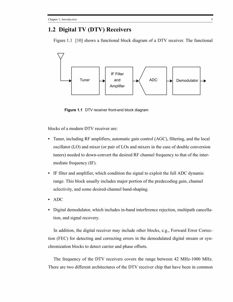
1.2 Digital TV (DTV) Receivers
Figure 1.1
Figure 1.1 DTV receiver front-end block diagram
IF Filterand
AmplifierADC DemodulatorTuner
[10] shows a functional block diagram of a DTV receiver. The functional
blocks of a modern DTV receiver are:
• Tuner, including RF amplifiers, automatic gain control (AGC), filtering, and the local
oscillator (LO) and mixer (or pair of LOs and mixers in the case of double conversion
tuners) needed to down-convert the desired RF channel frequency to that of the inter-
mediate frequency (IF).
• IF filter and amplifier, which condition the signal to exploit the full ADC dynamic
range. This block usually includes major portion of the predecoding gain, channel
selectivity, and some desired-channel band-shaping.
• ADC
• Digital demodulator, which includes in-band interference rejection, multipath cancella-
tion, and signal recovery.
In addition, the digital receiver may include other blocks, e.g., Forward Error Correc-
tion (FEC) for detecting and correcting errors in the demodulated digital stream or syn-
chronization blocks to detect carrier and phase offsets.
The frequency of the DTV receivers covers the range between 42 MHz-1000 MHz.
There are two different architectures of the DTV receiver chip that have been in common
Chapter 1: Introduction 6
use in the industry: (1) single-conversion; see Figure 1.2, and (2) double-conversion; see
Figure 1.3
Figure 1.2 Single-conversion DTV receiver block diagram example
ADC Demodulator
SAW Filter(Centred at 44 MHz)
Input RF Amplifier
FilterMixer
IF AmplifierFilter
IF Amplifier(TV Channnel)
LO(44MHz above the TV channel)
Tracking
Figure 1.3 Double-conversion DTV receiver block diagram example
ADC Demodulator
SAW Filter(Centred at 44 MHz)
Input RF Amplifier Mixer
2nd IF AmplifierFilter
1st IF Amplifier
LO(1.2GHz above the TV channel)
SAW Filter(Centred at 1.2 GHz)
Mixer
LO(44MHz below the 1st IF)
The single-conversion architecture directly down-converts the RF signal to an IF
(about 44 MHz). The single-conversion receivers rely on front-end “tracking filters” for
Chapter 1: Introduction 7
image suppression. Often, these filters are divided in to Low VHF, high VHF, and UHF
bands to cover the whole frequency range. The single-conversion architecture, which tra-
ditionally is implemented with Bipolar or Bi-CMOS processes, has been widely used in
DTV tuner ICs [4][9].
The double-conversion DTV receiver architecture up-converts the RF signal to an IF,
which is higher than the highest frequency in the input frequency range (about 1.2 GHz),
and then, using a fixed frequency mixer, down-converts the IF to a second IF (about 36
MHz - 44 MHz). Though, dual-conversion architecture can realize high image-rejection, it
suffers from high power consumption. In addition two off-chip SAW filters are usually
required for signal selection and image rejection, and these external filters limit the inte-
gration level and add to the cost of the receiver.
A direct-conversion receiver architecture for the European digital video broadcasting
for hand-held (DVB-H) has been proposed in [7]. An off-chip band-limit filter at the input
is used to suppress the undesired signals, and an external LNA has been employed to sat-
isfy the noise requirement. The IC uses on-chip eighth order, inverse Chebyshev low-pass
filtering for channel selectivity, and RF tunable bandpass filter and a polyphase mixer for
harmonic rejection. The I/Q mismatch errors have been addressed by the digital signal
processing (DSP) in the demodulator, but frequency-dependent errors have been mini-
mized by circuit design and layout. The IC has integrated a DC-offset correction system.
Image rejection and channel filtering have been implemented digitally. The receiver is
implemented in a 0.35μm SiGe BiCMOS technology and consumes 240 mW from a
2.775V supply.
A dual-conversion multi-standard analog and digital TV architecture has been reported
in [5]. The receiver consists of an up-conversion mixer, a digitally gain-programmable
image reject down-conversion mixer, and relies on two external first- and second-IF SAW
filters for channel filtering. The receiver is implemented in a 0.35mm SiGe BiCMOS tech-
nology and consumes 1.5W from a split 5V and 3.3V supply.
Chapter 1: Introduction 8
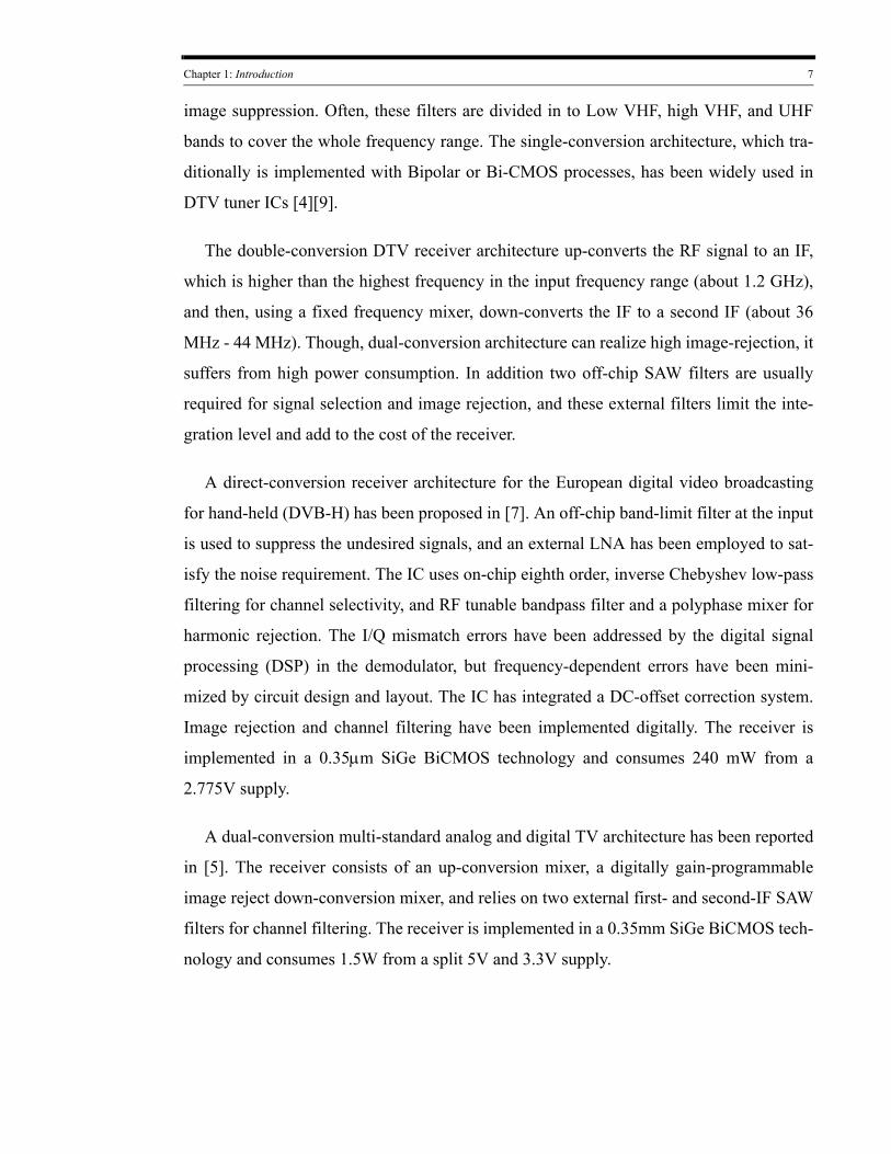
Besides the single- and double-conversion architectures, other architectures have been
reported in the literature. A double conversion zero second-IF (DZIF) DVB-T receiver
Figure 1.4 Double-conversion DTV receiver block diagram [2]
SAW Filter(1.22GHz)
Balun LNA MixerIF
Amplifier IF
Amplifier (0-4 MHz)
Dig
ital I
P
ADC
ADC(0-4 MHz)
Analog BasebandMixer
(1.22GHz)Quartz(27 MHz)
LO1 LO2(Quad)(1-26 - 2.08 GHz)
chip has been reported in [2]; refer Figure 1.4. In this architecture, the desired RF signal is
first up-converted to an intermediate frequency of 1.22GHz and then quadrature down-
converted to a zero intermediate frequency. Channel filtering is partially performed by an
external SAW filter centered at the first intermediate frequency. The I and Q outputs of the
quadrature mixer are digitized by two 14bits 4MHz bandwidth ΔΣ ADC modulators. The
IQ gain mismatch is corrected in the analog domain, and the phase mismatch is corrected
by digital algorithms processing the ADC outputs. The receiver has been implemented in a
2.5V, 0.12μm CMOS technology and consumes 1.4W.
A double-conversion, low-IF, multi-standard TV receiver chip has been reported in [6].
The proposed receiver uses an up-conversion followed by a quadrature down-conversion
mixer to shift the desired channel to a frequency of 1.75MHz. The complex outputs of the
quadrature mixer are filtered with a complex low-pass filter and finally digitized by two
11bit ADCs. The chip does not use any external SAW filters, and channel filtering and in-
Chapter 1: Introduction 9
band image rejection are performed in the digital domain. The receiver, which is fabri-
cated in a 0.25μm CMOS technology, consumes 1W from a 2.5V supply.
Over the past few years, there has been a marked shift from high-IF dual-conversion to
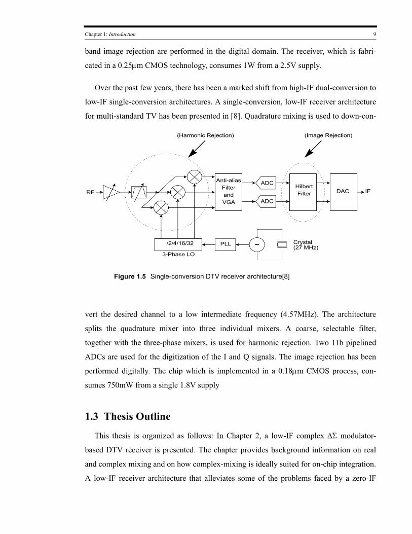
low-IF single-conversion architectures. A single-conversion, low-IF receiver architecture
for multi-standard TV has been presented in [8]
Figure 1.5 Single-conversion DTV receiver architecture[8]
RF
3-Phase LO
PLL Crystal
Anti-aliasFilterandVGA
(Harmonic Rejection)
HilbertFilter DAC
ADC
ADC
(Image Rejection)
/2/4/16/32
IF
(27 MHz)
. Quadrature mixing is used to down-con-
vert the desired channel to a low intermediate frequency (4.57MHz). The architecture
splits the quadrature mixer into three individual mixers. A coarse, selectable filter,
together with the three-phase mixers, is used for harmonic rejection. Two 11b pipelined
ADCs are used for the digitization of the I and Q signals. The image rejection has been
performed digitally. The chip which is implemented in a 0.18μm CMOS process, con-
sumes 750mW from a single 1.8V supply
1.3 Thesis Outline
This thesis is organized as follows: In Chapter 2, a low-IF complex ΔΣ modulator-
based DTV receiver is presented. The chapter provides background information on real
and complex mixing and on how complex-mixing is ideally suited for on-chip integration.
A low-IF receiver architecture that alleviates some of the problems faced by a zero-IF
Chapter 1: Introduction 10
receiver is presented. A major problem faced by receivers handling wireless signals is the
presence of interfering signals or “interferers”, which are usually stronger than the desired
signal, and accompany the desired signal. Often, intermodulation products generated by
these interferers and the desired signal limit the SNR of the receiver. After a discussion of
the “interfering signals” problem in DTV receivers, the chapter presents and compares the
existing approaches used to filter interfering signals in ΔΣ modulator ADC-based receiv-
ers. Finally, the chapter concludes by deriving specifications for a low-IF complex ΔΣ
modulator ADC suitable for a DTV receiver.
Chapter 3 starts with background information on the L 1 norm and how it can be used
in the design of an NTF. The chapter discusses the trade-off involved in the design of an
NTF and an STF; further, the need for developing an NTF-STF co-design methodology is
explained. The chapter presents design methodology for deriving NTFs, and STFs (real
and complex) with significant stop-band attenuations. Finally, the advantages of the pro-
posed ΔΣ ADC modulator with filtering STF are presented.
In Chapter 4, architecture-level design and simulations of the proposed ΔΣ modulator
are presented. The impact of circuit mismatches on a complex ΔΣ ADC modulator and the
need for stage-ordering are presented. The complete fourth order ΔΣ ADC modulator
architecture is presented in this chapter. The transition from the SimulinkTM [12] model to
the switched-capacitor (SC) circuit is presented. There is consideration of the impact of
SC circuit non-idealities, e.g., the settling errors of the integrators, finite gain of the
Opamp, finite resistance of the sampling switches, random jitter in the sampling clock,
capacitor mismatches,and multi-level DAC nonlinearity, on the SC circuit specifications.
Chapter 5 presents the circuit-level design and simulation of the blocks proposed in
Chapter 4. The circuit of the SC ΔΣ ADC modulator consists mainly of opamp, multi-bit
quantizer, multi-level DAC, non-overlapping clock generators, switches, and biasing. A
detailed description of the design of the various blocks in the SC ΔΣ ADC modulator is
presented. Finally, the layout techniques for capacitors, switches, quantizers, Opamp and
the complete fourth order modulator are presented.

Chapter 1: Introduction 11
Chapter 6 describes the experimental testing of the fabricated chip. The test set-up,
including the fabricated chip, and the designed printed circuit board (PCB), is presented in
the chapter. The measured results are also reported.
Chapter 7 concludes the thesis and suggests directions for future research.
Chapter 1: Introduction 12
References[1] Iuri Mehr, “Integrated TV Tuner Design for Multi-Standard Terrestrial Reception,”
IEEE Radio Frequency Integrated Circuits Symposium, pp. 75-78, June 2005
[2] D.Saias, F. Montaudon, E. Andre, F. Bailleui, M. Bely, P. Busson, S. Dedieu, A. Dezzani, A. Moutard, G. Provins, E. Rouat, J. Roux, G. Wagner, F. Paillardet, “A 0.12um CMOS DVB-T tuner,” IEEE International Digest of Technical Papers. ISSCC, pp.430-431, 2005
[3] Mark Dawkins, Alison Payne Burdett, NickCowley, “A Single-Chip Tuner for DVB-T,” IEEE Journal of Solid-State Circuits, vol. 38, No. 8, pp. 1307-1317, Aug. 2003.
[4] H. van Rumpt, D. Kasperkovitz, J. van der Tang, B. Nauta,“UMTV: a Single Chip TV receiver for PDAs, PCs, and Cell Phones,” IEEE International Digest of Technical Papers. ISSCC, pp.428-429, Feb. 2005
[5] Jan-Michael Stevenson, Phil Hisayasu, Armin Deiss, Buddhika Abesingha, Kim Beumer, Jose Esquivel, “Α Μulti-Standard Analog and Digital TV Tuner for Cable and Terrestrial Applications,” IEEE International Digest of Technical Papers. ISSCC, pp.210-213, Feb. 2007.
[6] Chun-Huat Heng, Manoj Gupta, Sang-Hoon Lee, David Kang, Bang-Sup Song, “ΑCMOS TV Tuner/Demodulator IC with Digital Image Rejection,” IEEE International Digest of Technical Papers. ISSCC, pp.432-433, Feb. 2005
[7] P. Antoine, P. Bauser, H. Beaulaton, M. Buchholz, D. Carey, T. Cassagnes, T.K. Chan, S. Colomines, F. Hurley, D. Jobling, N. Kearney, A. Murphy, J. Rock, D. Salle, C-T. Tu, “A Direct-Conversion Receiver for DVB-H,” IEEE International Digest of Technical Papers. ISSCC, pp.426-427, Feb. 2005
[8] Manoj Gupta, S. Lerstaveesin, D. Kang, B-S. Song, “Α 48-to-860MHz Direct-Conversion TV Tuner,” IEEE International Digest of Technical Papers. ISSCC, pp.206-208, Feb. 2007
[9] TUA 9001, RF Silicon Tuner for DVB-H/T and CMMB (Direct Conversion Receiver), INFINEON Technologies.
[10] J.G.N. Henderson, W.E. Bretl, M.S. Deiss, M.S. Goldberg, B. Markwalter, M. Muterspaugh, A. Touzni, “ATSC DTV Receiver Implementation,” Proceedings of the IEEE, vol . 94, issue 1, pp. 119- 147, Jan. 2006
[11] S. Mirabbasi and K. Martin, “Classical and Modern Receiver Architectures,” IEEE Communications Magazine, Nov 2000, pp. 132-139.
[12] The Math Works, Inc., Matlab, Version R2007a, Natick, Massachusetts: The Math Works, Inc., 2007.
CHAPTER
A Low-IF Complex ΔΣ ADC-based DTV
Receiver
This chapter provides background information regarding the “image-band problem”
that is related to frequency conversion, complex filters, mismatch issues associated with
complex filters, and “interfering-signals problem” in wireless receivers.
As the analog television broadcast system is being phased out and replaced by all-digi-
tal transmission in recent years, research has been conducted to develop digital television
(DTV) receivers. However, for the available DTV receiver solutions, the issues of low-
power and low-cost design still remain there. For example, most commercial DTV receiv-
ers use a dual-conversion architecture and are implemented with expensive technologies
like SiGe and BiCMOS, instead of with low-cost CMOS technology. These receivers rely
on external surface-acoustic wave (SAW) filters for image rejection and channel selection.
This chapter presents a low-IF complex ΔΣ modulator-based receiver architecture suitable
for realization of a highly integrated DTV receiver with CMOS technology.
Signals seen at the front-end of a wireless receiver typically consist of a desired signal
accompanied by strong interfering signals. Though ΔΣ ADCs with wide dynamic range
are suitable for digitizing such signals, there is often a need to pre-filter these signals due
to the linearity and power requirements of the analog circuits. This chapter reviews some
of the solutions for handling the interfering signals in ΔΣ modulator-based wireless receiv-
ers and presents their advantages and disadvantages. The benefits of ΔΣ ADC with inte-
gral filtering for digitizing signals accompanied by high interfering signals are outlined. In
2
13
Chapter 2: A Low-IF Complex ΔΣ ADC-based DTV Receiver 14
the next chapter, a design methodology for the realization of a ΔΣ modulator with a filter-
ing signal transfer function (STF) is presented.
2.1 Background
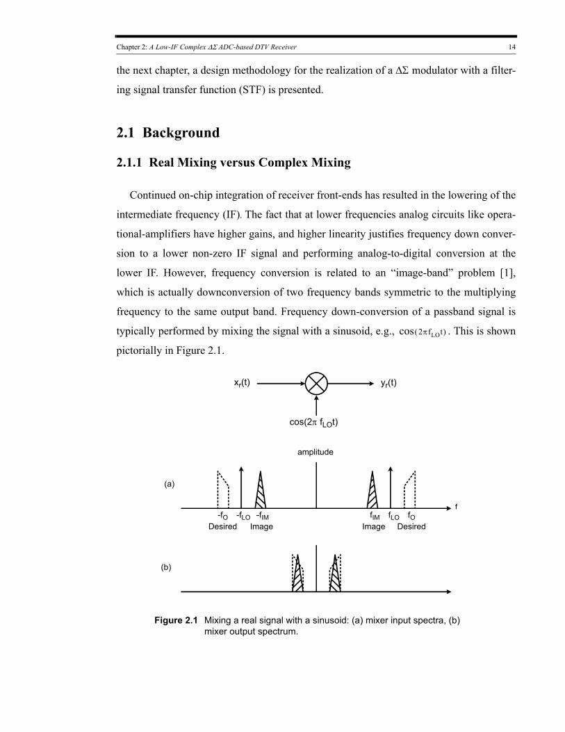
2.1.1 Real Mixing versus Complex Mixing
Continued on-chip integration of receiver front-ends has resulted in the lowering of the
intermediate frequency (IF). The fact that at lower frequencies analog circuits like opera-
tional-amplifiers have higher gains, and higher linearity justifies frequency down conver-
sion to a lower non-zero IF signal and performing analog-to-digital conversion at the
lower IF. However, frequency conversion is related to an “image-band” problem [1],
which is actually downconversion of two frequency bands symmetric to the multiplying
frequency to the same output band. Frequency down-conversion of a passband signal is
typically performed by mixing the signal with a sinusoid, e.g., 2πfLOt( )cos . This is shown
pictorially in Figure 2.1.
Figure 2.1 Mixing a real signal with a sinusoid: (a) mixer input spectra, (b) mixer output spectrum.
xr(t) yr(t)
cos(2π fLOt)
amplitude
ffLO-fLO
DesiredImage fOfIM-fIM-fO
(a)
(b)
Desired Image
Chapter 2: A Low-IF Complex ΔΣ ADC-based DTV Receiver 15
The spectrum of the mixer output signal is the superposition of the positive and negative
shifted versions of the spectrum of the input signal. As is shown in Figure 2.1, the two
frequency bands that are symmetrical around the multiplying frequency are down-
converted to the same output band. The undesired input signal band, which will be
superimposed on the desired signal band after mixing, is called the “image-band.” It is
necessary to suppress any signal in the image band prior to the mixing operation. This is
the task of the image-reject (IR) filter, which usually precedes the mixer.
The previously discussed image problem arises due to the fact that the frequency spec-
trum of a real sinusoid contains impulses at both positive and negative frequencies. One
way to avoid this problem is to mix the signal with a complex exponential, e.g., e-j2πfLOt ,
which has only a single frequency component, in this case at a negative frequency, fLO– .
Therefore, mixing a real signal with this negative-frequency complex exponential results
in a complex signal whose spectrum is a shifted version of the real signal spectrum. Theo-
retically, this process eliminates the image problem associated with frequency shifting
when mixing is done with a real sinusoid. Although a quadrature signal path is needed for
suppression of signals at the image frequency, this topology is still favorable due to perfor-
mance and efficiency in terms of power consumption. Almost all modern receivers
employ quadrature demodulation. The quadrature demodulation is performed by an I/Q
mixer that uses two local oscillators with a same frequency, but a 90° phase difference.
The I and Q components are independent and orthogonal to each other.
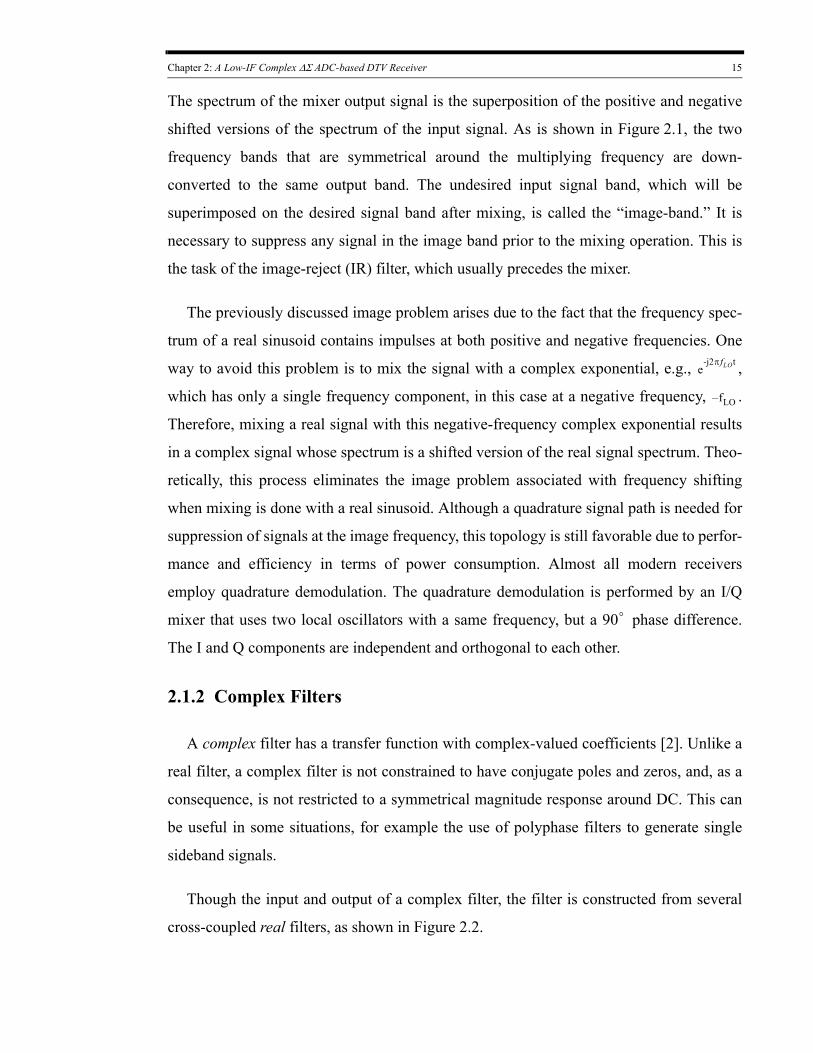
2.1.2 Complex Filters
A complex filter has a transfer function with complex-valued coefficients [2]. Unlike a
real filter, a complex filter is not constrained to have conjugate poles and zeros, and, as a
consequence, is not restricted to a symmetrical magnitude response around DC. This can
be useful in some situations, for example the use of polyphase filters to generate single
sideband signals.
Though the input and output of a complex filter, the filter is constructed from several
cross-coupled real filters, as shown in Figure 2.2.
Chapter 2: A Low-IF Complex ΔΣ ADC-based DTV Receiver 16
Are(z)
Are(z)
Aim(z)
Aim(z)
Xre(z)
Xim(z)
Yre(z)
Yim(z)
A(z)
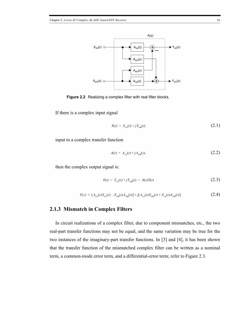
Figure 2.2 Realizing a complex filter with real filter blocks.
If there is a complex input signal
X z( ) Xre z( ) jXim z( )+= (2.1)
input to a complex transfer function
A z( ) Are z( ) jAim z( ),+= (2.2)
then the complex output signal is:
Y z( ) Yre z( ) jYim z( )+ A z( )X z( )= =
Y z( ) Are z( )Xre z( ) Xim z( )Aim z( )–[ ] j Are z( )Xim z( ) Xre z( )Aim z( )+[ ]+=
(2.3)
(2.4)
2.1.3 Mismatch in Complex Filters
In circuit realizations of a complex filter, due to component mismatches, etc., the two
real-part transfer functions may not be equal, and the same variation may be true for the
two instances of the imaginary-part transfer functions. In [3] and [4], it has been shown
that the transfer function of the mismatched complex filter can be written as a nominal
term, a common-mode error term, and a differential-error term; refer to Figure 2.3.
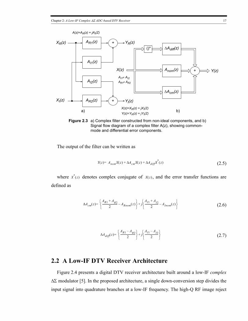
Chapter 2: A Low-IF Complex ΔΣ ADC-based DTV Receiver 17
a) b)
XR(z)
XI(z)
AR1(z)
AI1(z)
AI2(z)
AR2(z)
+
+
YR(z)
YI(z)
Y(z)=YR(z) + jYI(Z)
A(z)=AR(z) + jAI(Z)
AR1≠ AR2
AI1≠ AI2
+
()* ΔAdiff(z)
Anom(z)X(z)
ΔAcm(z)
Y(z)
X(z)=XR(z) + jXI(Z)
Figure 2.3 a) Complex filter constructed from non-ideal components, and b) Signal flow diagram of a complex filter A(z), showing common-mode and differential error components.
The output of the filter can be written as
Y z( ) AnomX z( ) AcmX z( ) AdiffX* z( )Δ+Δ+= (2.5)
where X* z( ) denotes complex conjugate of X z( ) , and the error transfer functions are
defined as
Acm z( )ΔAR1 A+ R2
2------------------------- ARnom z( )–
⎩ ⎭⎨ ⎬⎧ ⎫
jAI1 A+ I2
2---------------------- AInom z( )–
⎩ ⎭⎨ ⎬⎧ ⎫
+=
Adiff z( )ΔAR1 A– R2
2------------------------
⎩ ⎭⎨ ⎬⎧ ⎫
jAI1 A– I2
2----------------------
⎩ ⎭⎨ ⎬⎧ ⎫
+=
(2.6)
(2.7)
2.2 A Low-IF DTV Receiver Architecture
Figure 2.4 presents a digital DTV receiver architecture built around a low-IF complex
ΔΣ modulator [5]. In the proposed architecture, a single down-conversion step divides the
input signal into quadrature branches at a low-IF frequency. The high-Q RF image reject
Chapter 2: A Low-IF Complex ΔΣ ADC-based DTV Receiver 18
filter in the traditional receiver architecture has been replaced by a relaxed low-Q band-
pass filter [6]. In the low-IF receiver, the IF has been modified to a low but non-zero fre-
quency value; the frequency value falls into the baseband signal-processing capabilities of
the analog circuits. An architecture based on low-IF eliminates some of the detrimental
effects, e.g., DC-offset, LO self-mixing, second order intermodulation, that are faced by
the direct-conversion scheme. The main drawback of the low-IF architecture is that the
image band interference is close to the desired signal, and it is difficult to separate the
image frequency from the desired signal through the use of relaxed low-Q bandpass fil-
ters. The mismatches between the in-phase (I) and quadrature (Q) channels cause an alias-
ing of the image frequency into the desired channel. Since the image frequency can be
significantly stronger than the desired signal, the image rejection requirements of the
receiving system may demand a higher matching of the in-phase (I) and quadrature (Q)
channels.
Figure 2.4 A quadrature-IF system using a complex Low-IF ΔΣ modulator.
LO
ADC
VGAMixer
Amplifier
00
Mixer
900
ComplexBandpassΔΣ−
VGA
IF Polyphase Filter
Demodulator
Relaxed BP Filter
The dual ADCs in the traditional low-IF receiver architecture have been replaced by a
complex low-IF ΔΣ ADC. The low-IF has been selected at a value of 3 MHz for ATSC
and 4 MHz for DVB-T standards. At a maximum sampling frequency of 128 MHz, and an
over-sampling ratio (OSR) of 16, the architecture is suitable for digitization of the maxi-
mum DTV signal bandwidth of 8 MHz. The two anti-alias filters in the traditional dual
ADC architecture have been replaced by a single complex bandpass anti-aliasing filter,
and the replacement is advantageous since the same complex bandpass filter can be
Chapter 2: A Low-IF Complex ΔΣ ADC-based DTV Receiver 19
designed for alias rejection and also for image signals rejection. A low-IF means lower Q
bandpass poles, practical resistor and capacitor ratios, and a low sensitivity of the band-
pass filter center frequency to the errors in the RC time constants.
Among the wide variety of high-resolution ADC architectures, ΔΣ ADCs, with their
reduced sensitivity to component mismatches and lower power dissipation, are becoming
increasingly popular in systems that have stringent performance requirements such as
wide dynamic range, wide bandwidth, and low power. The presence of interferers puts a
severe demand on the linearity requirements of the analog circuitry in a wireless receiver,
and often the intermodulation products generated due to the non-linearities of the receiver
limit the system’s signal-to-noise ratio (SNR). An advantage of ΔΣ ADCs over other ADC
architectures is that for a given dynamic range over a narrow passband and sufficient lin-
earity to accommodate interferers over a large frequency band, ΔΣ ADCs tend to consume
less power than other ADC architectures that have comparable linearity but achieve the
full dynamic range over a larger frequency band [7]. With a large dynamic range and high
linearity, ΔΣ ADCs allow for reduced analog baseband components and transfer much of
the baseband filtering from the analog to the digital domain.
In a receiver system based on dual “one-input and one-output” ΔΣ modulators, the
same ΔΣ modulator performs analog-to-digital conversion on not only the signal compo-
nent but also on an image component. In contrast, a complex ΔΣ modulator, with no con-
straints of poles and zeros to be in conjugate pairs, digitizes only the signal component.
For a given OSR and sampling rate, the complex ΔΣ ADC signal bandwidth is effectively
halved and this halving translates into almost double the power efficiency as compared
with a dual ΔΣ ADC approach. Further, with a multi-bit complex quantizer and a multi-
level digital-to-analog converter (DAC), the requirements for performance of the internal
operational amplifiers are moderate, and a larger SNR can be implemented by a low-order
loop filter. The main advantages of a complex low-IF architecture are that offset and also
flicker noise do not interfere with the desired signal; self-EMI is not an issue because the
local-oscillator frequency is different from the carrier frequency. As in any bandpass sys-
tem, only odd-order distortion products have an effect. A complex-IF mixer alleviates the
Chapter 2: A Low-IF Complex ΔΣ ADC-based DTV Receiver 20
image problem, so that the front-end filter can have relaxed specifications and thus
reduced size.
DSP algorithms at the digital backend can be employed to compensate for I/Q imbal-
ance, complex down-conversion, equalization, etc. Furthermore, signal processing, like
channel selection, demodulation are performed in the digital domain, and this feature
gives the architecture the advantages of flexibility with respect to multi-standards.
2.3 The ‘Interfering Signals’ Problem in Wireless Receivers
A typical RF signal received at the input of a wireless receiver consists of a desired sig-
nal along with numerous interfering signals, which are usually stronger than the desired
signal. The ATSC Receiver Performance Guidelines [8] describe the minimum desired-to-
undesired (D/U) channel ratio, under which the DTV receivers should exceed the refer-
ence bit-error-rate (BER)1. For example, according to [8], there can be an interferer six
channels (36 MHz) away that has 57 dB higher power than the desired channel.
Similarly, DVB-T/H receiver standards [9] define signal reception conditions in the
presence of other interfering digital and analog TV channels. DVB-T [9] defines two dif-
ferent interference pattern sets that may be used to test the immunity of the DTV receiver
to interferences. The first set, which tests the selectivity of the receivers, includes two sep-
arate interferer patterns, i.e., S1 and S2:
• S1 pattern: analog interference signals from PAL/SECAM TV (S1 pattern), especially
PALG interference, defined as 35 dB stronger than the wanted 64-QAM signal. The
carrier of the analog TV signal is located a single channel away from the center of the
wanted signal;
• S2 pattern: a digital TV channel two channels away and up to 40 dB stronger than the
wanted signal.
1. At this BER level, the error protection can correct most of the data errors and deliver a high quality pic-ture.
Chapter 2: A Low-IF Complex ΔΣ ADC-based DTV Receiver 21
For a low-IF receiver architecture, these requirements translate into sharp channel
select filters and high linearity of the receiver.
The second set tests the non-linearity of the receiver with three different interferer pat-
terns: L1, L2, and L3, each consisting of two interferers:
• one digital interferer and one analog interferer, two and four channels away from the
wanted channel. The interfering channels can be 40 and 45 dB stronger than the wanted
signal;
• two analog interferers, two and four channels away from the wanted channel. The inter-
fering channels can be 45 dB stronger than the wanted signal;
• two digital interferers, two and four channels away from the wanted channel. The inter-
fering channels can be 40 dB stronger than the wanted signal.
The presence of other interfering signals, e.g., GSM interference from cell-phone up-
link, add to the linearity and filtering requirements of the receiver.
In addition, the receiver’s non-linearity can also generate interferences to DTV recep-
tion. The inter-modulation among the interfering channels or cross-modulation between
the interfering channels and the desired channel creates distortion or noise components
that fall in the desired channel. For example, interference from undesired signals on chan-
nels in the form N+K and N+2K (N is the desired channel) can cause two third-order inter-
modulation products falling in the channels N and N+3K [10]. Narrow tracking filters for
rejecting these interfering signals are not amenable to silicon integration, and, as a result
there is a large frequency range of signals present at the input of an analog-to-digital con-
verter in a receiver. The receiver has to reject these interfering signals and detect the trans-
mitted bit sequence. The presence of interfering signals requires that the analog-to-digital
converters, in addition to handling large signal dynamic range and bandwidth, must have
sufficient linearity that intermodulation products and aliased harmonics of the interferers
do not impact the reference BER.
Chapter 2: A Low-IF Complex ΔΣ ADC-based DTV Receiver 22
2.4 Approaches to Filtering Interfering Signals in ΔΣ ADC based Receivers
The interfering signals accompanying a desired signal may be filtered by digital filters
processing the ADC output, or they may be suppressed by an analog filter at the input of
the ADC. An alternative topology includes filtering as an integral part of the ADC.
2.4.1 Filtering Interfering Signals in the Digital Domain
The first solution to handling interferers consists of using an analog-to-digital con-
verter, typically a ΔΣ ADC, with a relaxed broadband analog filter at the front-end. Due to
its inherently anti-aliasing nature, in a continuous-time ΔΣ ADC, an anti-aliasing analog
filter of a lower order may be sufficient to meet the alias suppression requirements of the
ADC. The analog signals at the input of the ADC comprise the desired signals and possi-
bly the adjacent channel’s interfering signals. The presence of interferers demands a high
bandwidth and a dynamic range for the ADC. Another requirement is for the analog cir-
cuits to be linear in order to prevent the intermodulation products of large interferers from
disturbing the reception of a desired weak channel.
The bulk of signal processing, for example, interference attenuation, channel selection,
digital demodulation, takes place in the digital domain. An advantage of handling channel
filtering and demodulation functions in the digital domain is that this method leads to flex-
ible multi-standard receiver architectures. Filters with sharp stop band roll-off and linear
phase characteristics can be easily synthesized in the digital domain. However, since, in
that case, the task of the digital filters, in addition to filtering the quantization noise,
includes attenuation of the interfering signals, the situation calls for digital filters of higher
complexity, which cause higher power dissipation. A possible way to reduce power dissi-
pation would be to adapt the order of the digital filter to the levels of the interfering sig-
nals, for example, reduction of the filter order for low interfering signal levels. However,
the required interferer power detection circuitry adds to the complexity of the receiver, and
there can also be transition errors when the order of the filter is changed.
Chapter 2: A Low-IF Complex ΔΣ ADC-based DTV Receiver 23
2.4.2 Filtering Interfering Signals in the Analog Domain
An analog filter at the input of an ADC may be used to attenuate the interferers, and the
dynamic range and the linearity requirements of the ADC are thus relaxed. However, a
serious drawback of the analog filters is the change of the filter characteristics due to pro-
cess variations, and there can be differences between identical circuits on the same chip-
this can lead to mismatches and image issues in a receiver. There is a need for tuning or
calibration to compensate for these process variations. The additional components add
noise and distortion, which degrade the sensitivity of the receiver. Further, the signal qual-
ity at the input of the ADC can suffer due to the limited phase and pass band shape charac-
teristics that can be implemented with analog filters. Unlike digital circuits, analog circuits
do not scale well with technology migration and also lack the flexibility required for mul-
tistandard receivers.
2.4.3 Filtering Interfering Signals with a Filtering STF
An alternative solution is designing the signal transfer function (STF) of the ΔΣ ADC
to provide a filtering transfer function. The ADC performs a filtering of the input signal
before generating the corresponding digital output. The DSP performs high order filtering
and channel selection at the ADC output. A filtering ADC relaxes the requirements of
both the filtering in the IF path and the filtering in the digital domain. With a filtering STF,
the ΔΣ ADC modulator reduces intermodulation of the desired signal and the interfering
signals at the input of the quantizer, and avoids the feedback of the high-frequency inter-
fering signals at the input of the modulator. As will be shown in Chapter 3, ΔΣ modulator
ADCs with filtering STF have significantly reduced intermodulation products caused by
the feedback DAC non-linearities. Due to these reduced intermodulation products, ΔΣ
modulator ADCs with filtering STF demonstrate higher SNDR for applications where the
input signal is accompanied by strong out-of-band interfering signals.
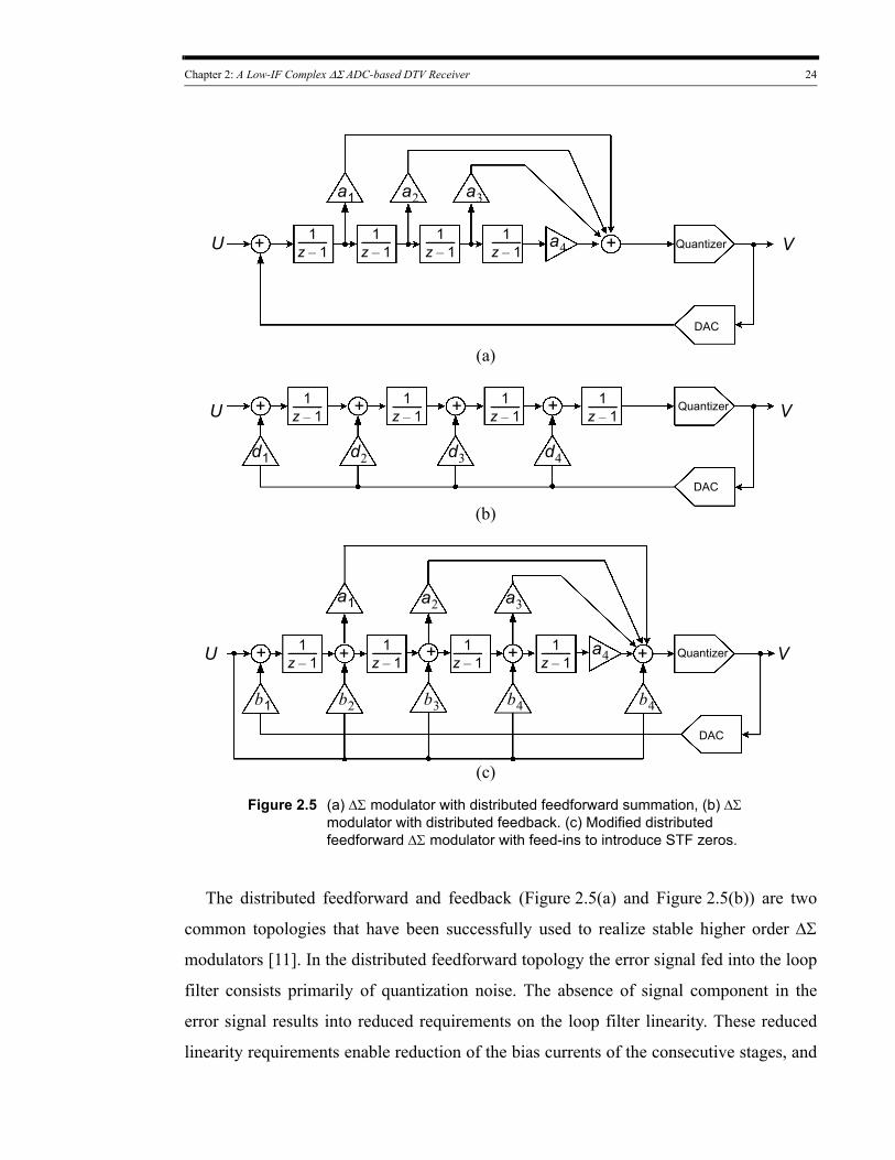
Chapter 2: A Low-IF Complex ΔΣ ADC-based DTV Receiver 24
Figure 2.5 (a) ΔΣ modulator with distributed feedforward summation, (b) ΔΣ modulator with distributed feedback. (c) Modified distributed feedforward ΔΣ modulator with feed-ins to introduce STF zeros.
(a)
(b)
(c)
1z 1–------------ 1
z 1–------------ 1
z 1–------------ 1
z 1–------------
1z 1–------------ 1
z 1–------------ 1
z 1–------------ 1
z 1–------------
1z 1–------------ 1
z 1–------------ 1
z 1–------------ 1
z 1–------------
a1 a2 a3
a4U V++
U
U
+ + + +
d1 d2 d4d3
b1 b2 b4b3
V
V+ + +
Quantizer
Quantizer
Quantizer
DAC
DAC
DAC
a1 a2 a3
a4+ +
b4
The distributed feedforward and feedback (Figure 2.5(a) and Figure 2.5(b)) are two
common topologies that have been successfully used to realize stable higher order ΔΣ
modulators [11]. In the distributed feedforward topology the error signal fed into the loop
filter consists primarily of quantization noise. The absence of signal component in the
error signal results into reduced requirements on the loop filter linearity. These reduced
linearity requirements enable reduction of the bias currents of the consecutive stages, and
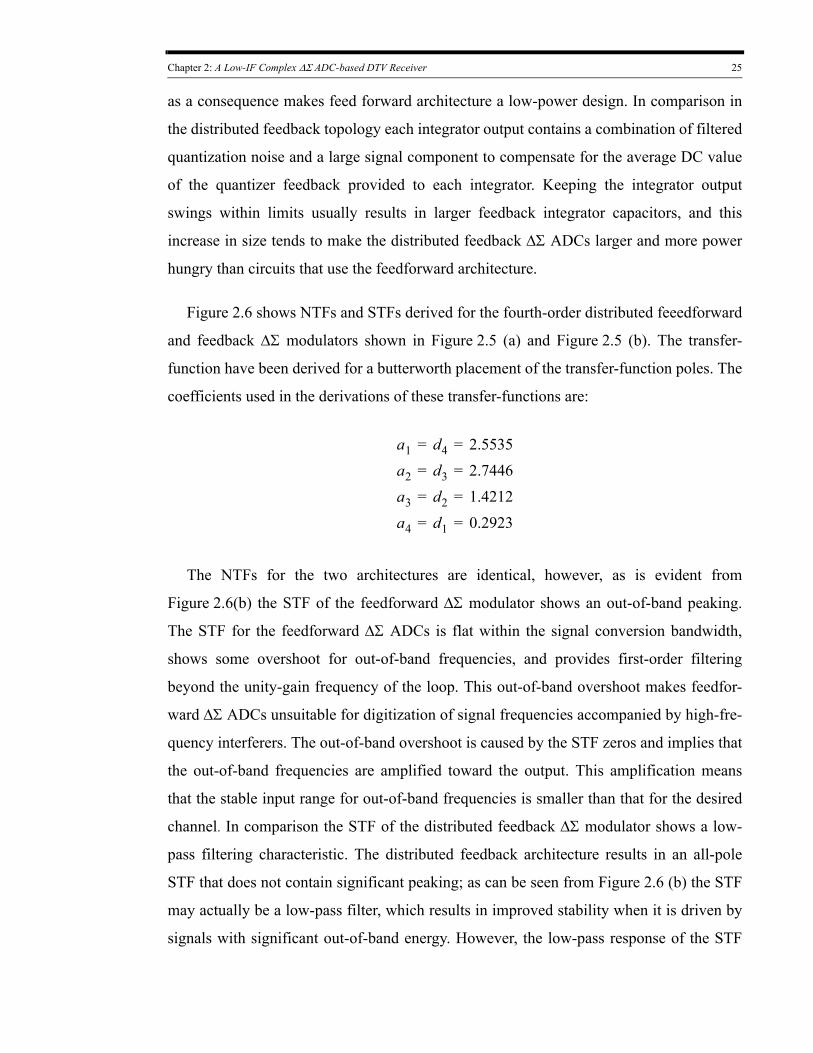
Chapter 2: A Low-IF Complex ΔΣ ADC-based DTV Receiver 25
as a consequence makes feed forward architecture a low-power design. In comparison in
the distributed feedback topology each integrator output contains a combination of filtered
quantization noise and a large signal component to compensate for the average DC value
of the quantizer feedback provided to each integrator. Keeping the integrator output
swings within limits usually results in larger feedback integrator capacitors, and this
increase in size tends to make the distributed feedback ΔΣ ADCs larger and more power
hungry than circuits that use the feedforward architecture.
Figure 2.6 shows NTFs and STFs derived for the fourth-order distributed feeedforward
and feedback ΔΣ modulators shown in Figure 2.5 (a) and Figure 2.5 (b). The transfer-
function have been derived for a butterworth placement of the transfer-function poles. The
coefficients used in the derivations of these transfer-functions are:
a1 = d4 = 2.5535a2 = d3 = 2.7446a3 = d2 = 1.4212a4 = d1 = 0.2923
The NTFs for the two architectures are identical, however, as is evident from
Figure 2.6(b) the STF of the feedforward ΔΣ modulator shows an out-of-band peaking.
The STF for the feedforward ΔΣ ADCs is flat within the signal conversion bandwidth,
shows some overshoot for out-of-band frequencies, and provides first-order filtering
beyond the unity-gain frequency of the loop. This out-of-band overshoot makes feedfor-
ward ΔΣ ADCs unsuitable for digitization of signal frequencies accompanied by high-fre-
quency interferers. The out-of-band overshoot is caused by the STF zeros and implies that
the out-of-band frequencies are amplified toward the output. This amplification means
that the stable input range for out-of-band frequencies is smaller than that for the desired
channel. In comparison the STF of the distributed feedback ΔΣ modulator shows a low-
pass filtering characteristic. The distributed feedback architecture results in an all-pole
STF that does not contain significant peaking; as can be seen from Figure 2.6 (b) the STF
may actually be a low-pass filter, which results in improved stability when it is driven by
signals with significant out-of-band energy. However, the low-pass response of the STF
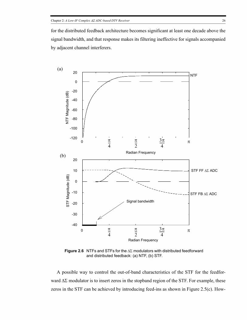
Chapter 2: A Low-IF Complex ΔΣ ADC-based DTV Receiver 26
for the distributed feedback architecture becomes significant at least one decade above the
signal bandwidth, and that response makes its filtering ineffective for signals accompanied
by adjacent channel interferers.
Figure 2.6 NTFs and STFs for the ΔΣ modulators with distributed feedforward and distributed feedback: (a) NTF, (b) STF.
20
0
-20
-40
-60
-80
-100
-1200 ππ
2--- 3π
4------π
4---
0 ππ2--- 3π
4------π
4---
20
10
0
-10
-20
-30
-40
STF FF ΔΣ ADC
STF FB ΔΣ ADC
Radian Frequency
NTF
Mag
nitu
de (d
B)S
TF M
agni
tude
(dB)
Radian Frequency
(a)
(b)
Signal bandwidth
NTF
A possible way to control the out-of-band characteristics of the STF for the feedfor-
ward ΔΣ modulator is to insert zeros in the stopband region of the STF. For example, these
zeros in the STF can be achieved by introducing feed-ins as shown in Figure 2.5(c). How-
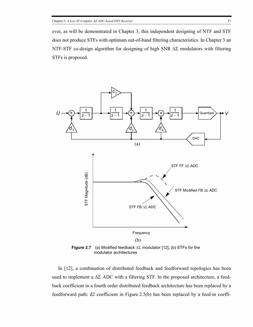
Chapter 2: A Low-IF Complex ΔΣ ADC-based DTV Receiver 27
ever, as will be demonstrated in Chapter 3, this independent designing of NTF and STF
does not produce STFs with optimum out-of-band filtering characteristics. In Chapter 3 an
NTF-STF co-design algorithm for designing of high SNR ΔΣ modulators with filtering
STFs is proposed.
Figure 2.7 (a) Modified feedback ΔΣ modulator [12], (b) STFs for the modulator architectures
(a)
1z 1–------------ 1
z 1–------------ 1
z 1–------------ 1
z 1–------------U
d1
c2
d4d3
V+ + + Quantizer
DAC
(b)
STF FF ΔΣ ADC
STF FB ΔΣ ADC
STF Modified FB ΔΣ ADC
Frequency
STF
Mag
nitu
de (d
B)
In [12], a combination of distributed feedback and feedforward topologies has been
used to implement a ΔΣ ADC with a filtering STF. In the proposed architecture, a feed-
back coefficient in a fourth order distributed feedback architecture has been replaced by a
feedforward path: d2 coefficient in Figure 2.5(b) has been replaced by a feed-in coeffi-
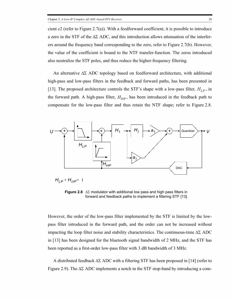
Chapter 2: A Low-IF Complex ΔΣ ADC-based DTV Receiver 28
cient c2 (refer to Figure 2.7(a)). With a feedforward coefficient, it is possible to introduce
a zero in the STF of the ΔΣ ADC, and this introduction allows attenuation of the interfer-
ers around the frequency band corresponding to the zero, refer to Figure 2.7(b). However,
the value of the coefficient is bound to the NTF transfer-function. The zeros introduced
also neutralize the STF poles, and thus reduce the higher-frequency filtering.
Figure 2.8 ΔΣ modulator with additional low pass and high pass filters in forward and feedback paths to implement a filtering STF [13].
+ + +a1
a2
U VQuantizer
DAC
H1 H2
HLP
HHP
HLP HHP 1=+
An alternative ΔΣ ADC topology based on feedforward architecture, with additional
high-pass and low-pass filters in the feedback and forward paths, has been presented in
[13]. The proposed architecture controls the STF’s shape with a low-pass filter, HLP , in
the forward path. A high-pass filter, HHP , has been introduced in the feedback path to
compensate for the low-pass filter and thus retain the NTF shape; refer to Figure 2.8.
However, the order of the low-pass filter implemented by the STF is limited by the low-
pass filter introduced in the forward path, and the order can not be increased without
impacting the loop filter noise and stability characteristics. The continuous-time ΔΣ ADC
in [13] has been designed for the bluetooth signal bandwidth of 2 MHz, and the STF has
been reported as a first-order low-pass filter with 3 dB bandwidth of 3 MHz.
A distributed feedback ΔΣ ADC with a filtering STF has been proposed in [14] (refer to
Figure 2.9). The ΔΣ ADC implements a notch in the STF stop-band by introducing a com-
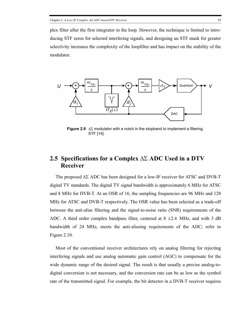
Chapter 2: A Low-IF Complex ΔΣ ADC-based DTV Receiver 29
plex filter after the first integrator in the loop. However, the technique is limited to intro-
ducing STF zeros for selected interfering signals, and designing an STF mask for greater
selectivity increases the complexity of the loopfilter and has impact on the stability of the
modulator.
Figure 2.9 ΔΣ modulator with a notch in the stopband to implement a filtering STF [14].
U + +
d1 d2
VQuantizer
DAC
ωug1
s----------
ωug2
s----------
HR s( )
a1
2.5 Specifications for a Complex ΔΣ ADC Used in a DTV Receiver
The proposed ΔΣ ADC has been designed for a low-IF receiver for ATSC and DVB-T
digital TV standards. The digital TV signal bandwidth is approximately 6 MHz for ATSC
and 8 MHz for DVB-T. At an OSR of 16, the sampling frequencies are 96 MHz and 128
MHz for ATSC and DVB-T respectively. The OSR value has been selected as a trade-off
between the anti-alias filtering and the signal-to-noise ratio (SNR) requirements of the
ADC. A third order complex bandpass filter, centered at 8 2.4± MHz, and with 3 dB
bandwidth of 24 MHz, meets the anti-aliasing requirements of the ADC; refer to
Figure 2.10.
Most of the conventional receiver architectures rely on analog filtering for rejecting
interfering signals and use analog automatic gain control (AGC) to compensate for the
wide dynamic range of the desired signal. The result is that usually a precise analog-to-
digital conversion is not necessary, and the conversion rate can be as low as the symbol
rate of the transmitted signal. For example, the bit detector in a DVB-T receiver requires
Chapter 2: A Low-IF Complex ΔΣ ADC-based DTV Receiver 30
only 27.5 dB of SNR to achieve the required 2 10 4–× BER. Therefore, a pair of flash ADCs
that each perform 5-bit uniform quantization sampling at Nyquist frequency would more
than suffice in a DVB-T receiver that performs quadrature down-conversion, with all fil-
tering and AGC in the analog domain. However, in integrated receivers, given the reduc-
tion in power consumption and circuit complexity that can be achieved by trading analog
processing for digital processing, the trend is to perform as much of the signal processing
as possible, e.g., channel selection etc., in the digital domain.
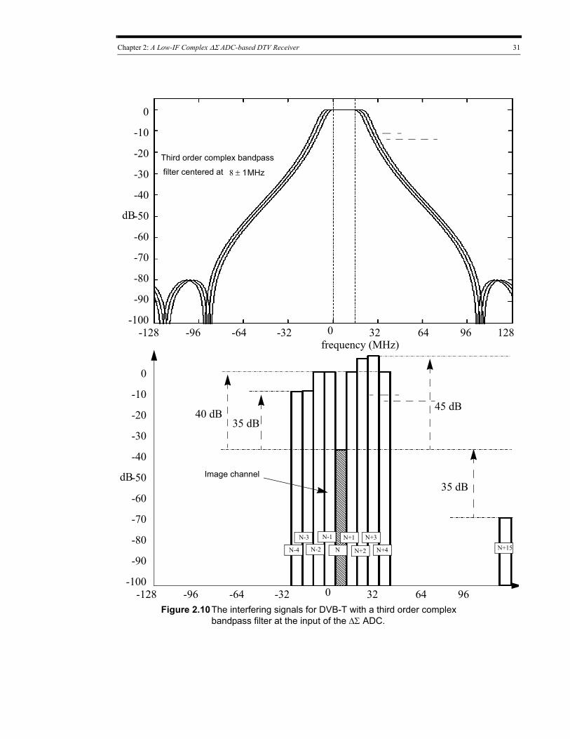
Chapter 2: A Low-IF Complex ΔΣ ADC-based DTV Receiver 31
0
-10
-20
-30
-40
-50
-60
-70
-80
-90
-100
-24 dB
Third order complex bandpass
filter centered at 8 1MHz±
Figure 2.10The interfering signals for DVB-T with a third order complex bandpass filter at the input of the ΔΣ ADC.
0 128
N+15
frequency (MHz)
dB
-128 64 -64 -96 32 96
Image channel
N+2
N+1 N+3
N+4N-2
N-3
-32
N-4 N
N-1
35 dB40 dB
35 dB
45 dB
0
-10
-20
-30
-40
-50
-60
-70
-80
-90
-1000
dB
-128 64 -64 -96 32 96 -32
Chapter 2: A Low-IF Complex ΔΣ ADC-based DTV Receiver 32
An advantage of this architecture is that the I/Q matching accuracy is very good,
depending basically on the matching of the ADC input stage. In addition, as the filters are
implemented digitally, they can have very accurate frequency response and linear phase
characteristic, which are important for digital modulation techniques. However, this
interchange of channel filtering and ADC greatly increases the dynamic range and
sample-rate required of the ADCs. ADCs with a resolution of more than 13-bits are
typically required. For example, DVB-T tuner sensitivity for a 8 MHz channel is
approximately -95 dBm for the QPSK scheme and -75 dBm for QAM scheme. In the
absence of any interference, the maximum wanted DVB-T signal for the tuner input is -28
dBm. Therefore, considering -95 dBm sensitivity, the receiver has to provide at least a
dynamic range of 67 dB.
The proposed low-IF receiver solution follows a variable gain amplifier (VGA) with
automatic gain control (AGC) and ADC approach. By distributing the receiver specifica-
tions between VGA and ADC, both the circuits can be designed with reduced complexi-
ties. With the analog front-end filter implemented as a broadband anti-aliasing filter, the
SNR requirements of the ADC are decided by the required adjacent-channel immunity.
The ADC samples signals comprising the desired signal, the image signal, and some adja-
cent signals.
The target SNR for the ADC has been determined in a way that is consistent with the
following considerations:
• For ATSC, the required desired-to-undesired signal ratio (D/U) for the adjacent channel
NTSC interference into the desired DTV channel is -40 dB [8]. For higher channels, the
maximum rejection threshold for DTV interference into DTV has been set at -48dB.
When a carrier-to-noise ratio (C/N) of 15.5 dB is maintained, the required SNR of the
ADC works out to be 63.5 dB.
• According to DVB-T standards, assuming 64-QAM and CR 3 4⁄= , the adjacent
channels (N 1± ) can be up to 35 dB stronger, while the channels (N 2± ) can be up to 43
dB stronger [9]. With the required carrier-to-noise ratio (C/N) of 27.5 dB for the refer-
Chapter 2: A Low-IF Complex ΔΣ ADC-based DTV Receiver 33
ence BER in the Rayleigh channel (P1), the dynamic range of the ADC is 62.5 dB.
When an extra headroom of 9 dB [15] is added to avoid clipping of the OFDM signal
due to peak to average ratio (PAR) variations, the SNR of the ADC is 71.5 dB.
The output of the ΔΣ ADC comprises the desired signal centered at the low-IF of 3
MHz or 4 MHz, depending on the DTV standard, the mirror signal, the interfering signals,
and the noise-shaped quantization noise. The final image rejection, down-conversion, and
baseband filtering are done with the DSP. The down-conversion to the baseband can be
performed by a double quadrature multiplication of the ΔΣ ADC output with a quadrature
IF signal [16]. This quadrature multiplication will down-convert the desired signal to the
baseband, centered around DC; however, it will also upconvert the mirror signal to the
baseband. Given the image resulting from the adjacent channel, an image rejection of 55.5
dB for ATSC and 62.5 dB for DVB-T is required of the digital down-converter. To have an
image rejection of higher than 62.5 dB, the ΔΣ ADC needs at least 11 bits of resolution.
2.5.1 Mismatch and Image Rejection Requirements of the Low-IF
Complex ΔΣ ADC
A complex ΔΣ modulator, like a complex filter suffers from mismatches in the I and the
Q paths. Due to mismatches, signal or noise at the image frequency aliases into signal
band of interest and this leads to the deterioration of the ADC SNR. Figure 2.11 is a block
diagram of a complex ΔΣ modulator with a mismatch in gain elements between the I and
Q paths of the modulator. In Figure 2.11, the complex ΔΣ modulator shown includes a
complex filter having a transfer function H(z), two quantizers, and two mismatched multi-
pliers with multiplication coefficients of 1 Δg– and 1 Δg+ . In the absence of mismatches
(Δg 0= ), the following equation is satisfied:
YI z( ) jYQ z( ) H z( )1 H z( )+--------------------- XI z( ) jXQ z( )+( ) 1
1 H z( )+--------------------- EI z( ) jEQ z( )+( )+=+ (2.8)
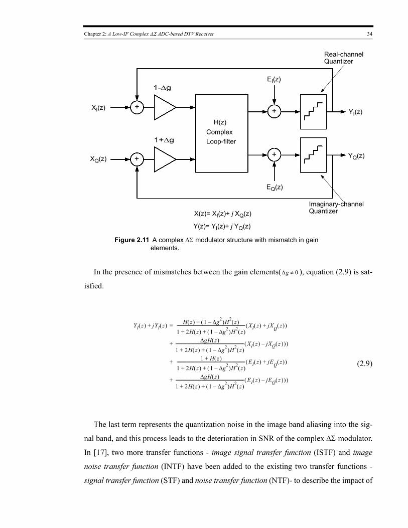
Chapter 2: A Low-IF Complex ΔΣ ADC-based DTV Receiver 34
Real-channelQuantizer
Figure 2.11 A complex ΔΣ modulator structure with mismatch in gain elements.
EI(z)
EQ(z)
XI(z)
ComplexH(z)
X(z)= XI(z)+ j XQ(z)
Loop-filter
XQ(z)
1-Δg
1+Δg
YI(z)
YQ(z)
Y(z)= YI(z)+ j YQ(z)
Imaginary-channelQuantizer
+
+ +
+
In the presence of mismatches between the gain elements(Δg 0≠ ), equation (2.9) is sat-
isfied.
YI z( ) jYI z( )+ = H z( ) 1 g2Δ–( )H2 z( )+1 2H z( ) 1 g2Δ–( )H2 z( )+ +-------------------------------------------------------------------- XI z( ) jX+ Q z( )( )
+ gHΔ z( )
1 2H z( ) 1 g2Δ–( )H2 z( )+ +-------------------------------------------------------------------- XI z( ) jXQ z )( )–( )
+ 1 H z( )+1 2H z( ) 1 g2Δ–( )H2 z( )+ +-------------------------------------------------------------------- EI z( ) jE+ Q z( )( )
+ gHΔ z( )
1 2H z( ) 1 g2Δ–( )H2 z( )+ +-------------------------------------------------------------------- EI z( ) jEQ z )( )–( )
(2.9)
The last term represents the quantization noise in the image band aliasing into the sig-
nal band, and this process leads to the deterioration in SNR of the complex ΔΣ modulator.
In [17], two more transfer functions - image signal transfer function (ISTF) and image
noise transfer function (INTF) have been added to the existing two transfer functions -
signal transfer function (STF) and noise transfer function (NTF)- to describe the impact of
Chapter 2: A Low-IF Complex ΔΣ ADC-based DTV Receiver 35
mismatches in a complex ΔΣ modulator. In the presence of mismatches the output of the
complex ΔΣ modulator can be written as [17]:
Y z( ) G z( )X z( ) GdiffX* z( ) H z( )E z( ) HdiffE
* z( )Δ+ +Δ+= (3)
ΔGdiff is the image signal transfer function, or ISTF, which determines the gain from
the image-signal input to the output, and ΔHdiff is the transfer function which determines
the gain from the quantization-noise input to the modulator output. Though the in-band
noise is shaped by the deep in-band notches of the NTF, the, image-band noise, which is
significantly larger than in-band noise, is shaped by the INTF. The results is that mis-
matches cause out-of-band quantization noise in the complex ΔΣ modulator to alias into
the in-band region. The INTF created by differential mismatch plays a critical role in
determining the SNR of the non-ideal modulator. One of the techniques to reduce the dif-
ferential error term HdiffΔ is to place one of the NTF notches in the quantizer’s own
image band; this method attenuates some of the image band noise, E* z( ) , before it aliases
into the signal band [17]. However, the other differential error term, GdiffΔ , does not
improve through the placement of the NTF notch in the image band, and strong interfer-
ence at image frequency can be aliased into the signal band.
Given the strength of the adjacent channel interferers and the desired carrier-to-noise
ratio, the image rejection requirements for the ΔΣ ADC work out to be 55.5 dB and 62.5
dB for ATSC and DVB-T standards respectively. Providing a safety margin to account for
other noise sources which will degrade the SNR of the ADC, a ΔΣ ADC with a dynamic
range of 75.0 dB, and image rejection better than 65 dB should be adequate for the digiti-
zation of the DTV signals in the proposed low-IF receiver.
Chapter 2: A Low-IF Complex ΔΣ ADC-based DTV Receiver 36
References[1] S. Mirabbasi and K. Martin, “Classical and modern receiver architectures,” IEEE
Communications Magazine, Nov 2000, pp. 132-139.
[2] Q. L. Liu, W. M. Snelgrove, and A.S. Sedra, “Switched-capacitor implementation of complex filters,” Proceedings of the 1986 IEEE ISCAS, vol. 3, pp. 1121-1124, May 1986.
[3] A. S. Sedra, W. M. Snelgrove, and R. Allen, “Complex analog bandpass filters designed by linearly shifting real low-pass prototypes,” Proceedings of the 1985 IEEE ISCAS, vol. 3, pp. 1223-1226, June 1985.
[4] R. H. Allen, “Complex analog filters obtained from shifted lowpass prototypes”, M.A.Sc. thesis, University of Toronto, 1985.
[5] S.A. Jantzi, K. Martin, and A.S. Sedra, “Quadrature bandpass DS modulation for digital radio,” IEEE J. Solid-State Circuits, vol. 32, pp. 1935-1949, Dec. 1997.
[6] J. Crols, M.S.J. Steyaert, ‘‘Low-IF topologies for high-performance analog front ends of fully integrated receivers,” IEEE Trans. Circuits Syst. -II: Analog and Digital Signal Processing, vol. 45, no. 3, pp. 269- 282, March 1998.
[7] I. Galton, “Delta-Sigma data conversion in wireless transceivers,” IEEE Transactions on Microwave Theory and Techniques, vol. 50. no.1, pp. 302-315 Jan 2002.
[8] ATSC Recommended Practice: Receiver Performance Guidelines, ATSC A/74, June 2004, pp 13-14.
[9] Mobile and Portable DVB-T/H Radio Access Interface Specification, EICTA MBRAI-02.
[10] G. Sgrignoli, C.W. Rhodes, “Interference mitigation for improved DTV reception,” IEEE Transactions on Consumer Electronics, vol. 51, no. 2, pp. 463-470.
[11] S. R. Norsworthy, R. Schreier, and G. C. Temes, Eds., Delta-Sigma Data Converters: Theory, Design, and Simulation. New York: IEEE Press. ISBN 0780310454.
[12] F. Munoz, K. Philips, and A. Torralba, ‘‘A 4.7mW, 89.5dB DR CT complex ΔΣADC with built-In LPF,” ISSCC Dig. Tech. Papers, pp. 500-501, Feb., 2005.
[13] K. Philips, P.A.C.M. Nuijten, R.L.J. Roovers, A.H.M. van Roermund, F.M. Chavero,M.T. Pallares, A. Torralba , ‘‘A 2mW, 89dB DR continuous-Time ΔΣADC with increased wide-band interference immunity,” ISSCC Dig. Tech. Papers, pp. 86-87, Feb., 2004.
[14] Y. Le Guillou, and H. Fakhoury, ‘‘Elliptic filtering in continuous-time sigma-delta modulator,” Electronics Letters, vol. 41, no. 4, pp. 167-168, 17th Feb., 2005.
[15] Hua Yu, Gang Wei, “Statistical distribution of the signal PAR in the practical OFDM systems,” International Conference on Communications, Circuits and Systems Proceedings, vol 2, 25-28, June. 2006, pp. 1235- 1239.
Chapter 2: A Low-IF Complex ΔΣ ADC-based DTV Receiver 37
[16] Chun-Huat Heng, Manoj Gupta, Sang-Hoon Lee, David Kang, Bang-Sup Song, “A CMOS TV tuner/demodulator IC with digital image rejection,” IEEE Journal of Solid-State Circuits, vol 40, no.12, Dec. 2005, pp. 2525- 2535.
[17] S.A. Jantzi, K. W. Martin, and A. S. Sedra, “The effects of mismatch in complex bandpass ΔΣ modulators,” IEEE International Symposium on Circuits and Systems, vol. 1, 12-15, May 1996, pp. 227-230.
CHAPTER
A Complex ΔΣ Modulator with an
Improved STF
The presence of interferers puts a severe demand on the linearity requirements of the
analog circuitry of a ΔΣ ADC and, in such applications, instead of unity signal-transfer
functions (STF), it may be more desirable to have an STF with improved out-of-band
attenuation. Depending on the application, e.g., single sideband (SSB), it may also be
desirable to have higher attenuation in image band frequencies. Historically, complex
transfer functions have been based on frequency transformations of real prototype filters.
However, because of arithmetical symmetry, such complex transfer functions are ineffi-
cient in meeting the asymmetric requirements of a wireless receiver.
The design of an STF with higher stop-band attenuation has an implication for the qual-
ity of the noise-transfer function (NTF). This chapter discusses the trade-off involved in
STF-NTF design.
The chapter further presents a methodology for designing arithmetically asymmetric
complex signal-transfer functions and noise transfer functions that use complex filter rou-
tines [1] based on classical filter design procedures. A complex ΔΣ modulator architecture
suitable for realizing the transfer functions that have been derived using the optimization
is presented. The modulator and the design methodology have been used to design a proto-
type modulator for the DTV (ATSC and DVB) specifications. The advantages of the pro-
posed ΔΣ modulator are presented.
3
38
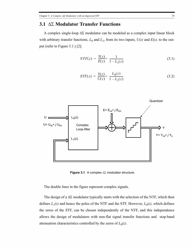
Chapter 3: A Complex ΔΣ Modulator with an Improved STF 39
3.1 ΔΣ Modulator Transfer Functions
A complex single-loop ΔΣ modulator can be modeled as a complex input linear block
with arbitrary transfer functions, L0 and L1, from its two inputs, U(z) and E(z), to the out-
put (refer to Figure 3.1.) [2]:
NTF z( ) Y z( )E z( )----------- 1
1 L1 z( )–----------------------==
STF z( ) Y z( )U z( )-----------
L0 z( )1 L1 z( )–----------------------==
Complex
L1(z)
Quantizer
U= Ure+ j UIm
Figure 3.1 A complex ΔΣ modulator structure.
U
Loop-filter
L0(z)
Y= Yre+ j YIm
E= Ere+ j EIm
Y
(3.1)
(3.2)
The double lines in the figure represent complex signals.
The design of a ΔΣ modulator typically starts with the selection of the NTF, which then
defines L1(z) and hence the poles of the NTF and the STF. However, L0(z), which defines
the zeros of the STF, can be chosen independently of the NTF, and this independence
allows the design of modulators with non-flat signal transfer functions and stop-band
attenuation characteristics controlled by the zeros of L0(z).
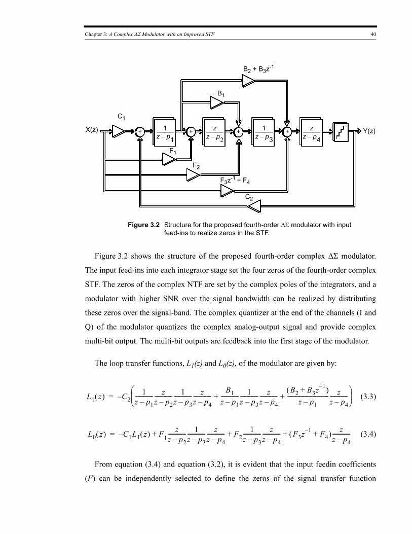
Chapter 3: A Complex ΔΣ Modulator with an Improved STF 40
F3z-1 + F4
F2
F1
B1
B2 + B3z-1
1z p1–--------------- z
z p2–---------------
C2
C1
X(z) 1z p3–--------------- z
z p4–---------------
Figure 3.2 Structure for the proposed fourth-order ΔΣ modulator with input feed-ins to realize zeros in the STF.
++++ Y(z)
Figure 3.2 shows the structure of the proposed fourth-order complex ΔΣ modulator.
The input feed-ins into each integrator stage set the four zeros of the fourth-order complex
STF. The zeros of the complex NTF are set by the complex poles of the integrators, and a
modulator with higher SNR over the signal bandwidth can be realized by distributing
these zeros over the signal-band. The complex quantizer at the end of the channels (I and
Q) of the modulator quantizes the complex analog-output signal and provide complex
multi-bit output. The multi-bit outputs are feedback into the first stage of the modulator.
The loop transfer functions, L1(z) and L0(z), of the modulator are given by:
L1 z( ) C– 21
z p1–------------- z
z p2–------------- 1
z p3–------------- z
z p4–-------------
B1z p1–------------- 1
z p3–------------- z
z p4–-------------
B2 B3z 1–+( )z p1–
------------------------------- zz p4–-------------+ +
⎝ ⎠⎜ ⎟⎛ ⎞
=
L0 z( ) C1L1 z( ) F+– 1z
z p2–------------- 1
z p3–------------- z
z p4–------------- F2
1z p3–------------- z
z p4–------------- F3z 1– F4+( ) z
z p4–-------------+ +=
(3.3)
(3.4)
From equation (3.4) and equation (3.2), it is evident that the input feedin coefficients
(F) can be independently selected to define the zeros of the signal transfer function
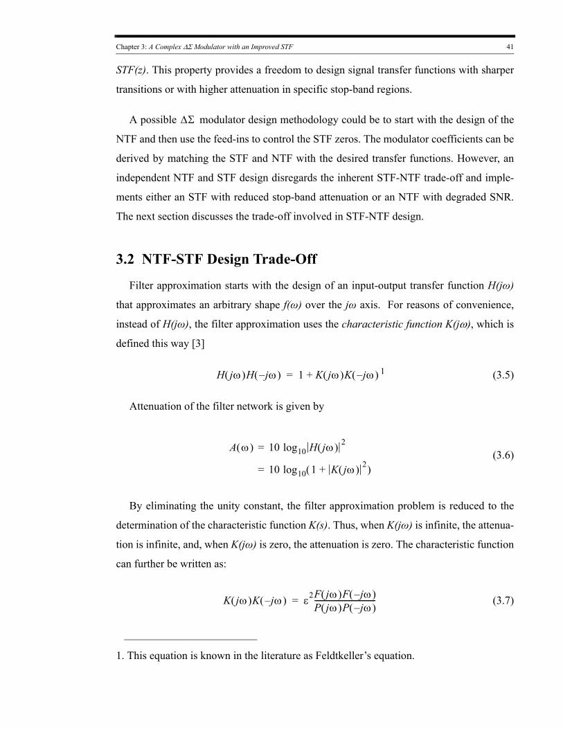
Chapter 3: A Complex ΔΣ Modulator with an Improved STF 41
STF(z). This property provides a freedom to design signal transfer functions with sharper
transitions or with higher attenuation in specific stop-band regions.
A possible ΔΣ modulator design methodology could be to start with the design of the
NTF and then use the feed-ins to control the STF zeros. The modulator coefficients can be
derived by matching the STF and NTF with the desired transfer functions. However, an
independent NTF and STF design disregards the inherent STF-NTF trade-off and imple-
ments either an STF with reduced stop-band attenuation or an NTF with degraded SNR.
The next section discusses the trade-off involved in STF-NTF design.
3.2 NTF-STF Design Trade-Off
Filter approximation starts with the design of an input-output transfer function H(jω)
that approximates an arbitrary shape f(ω) over the jω axis. For reasons of convenience,
instead of H(jω), the filter approximation uses the characteristic function K(jω), which is
defined this way [3]
H jω( )H jω–( ) 1 K jω( )K jω–( )+= 1 (3.5)
Attenuation of the filter network is given by
A ω( ) = 10 log10 H jω( ) 2
= 10 log10 1 K jω( ) 2+( ) (3.6)
By eliminating the unity constant, the filter approximation problem is reduced to the
determination of the characteristic function K(s). Thus, when K(jω) is infinite, the attenua-
tion is infinite, and, when K(jω) is zero, the attenuation is zero. The characteristic function
can further be written as:
K jω( )K jω–( ) ε2F jω( )F jω–( )P jω( )P jω–( )---------------------------------= (3.7)
1. This equation is known in the literature as Feldtkeller’s equation.
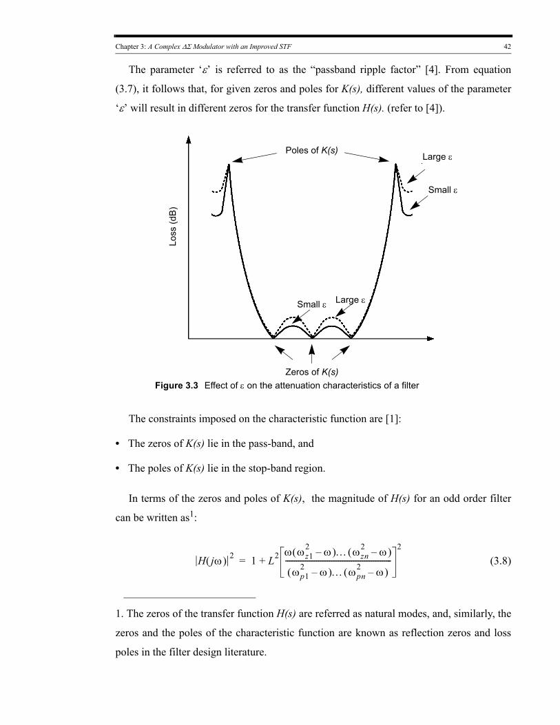
Chapter 3: A Complex ΔΣ Modulator with an Improved STF 42
The parameter ‘ε’ is referred to as the “passband ripple factor” [4]. From equation
(3.7), it follows that, for given zeros and poles for K(s), different values of the parameter
‘ε’ will result in different zeros for the transfer function H(s). (refer to [4])
Figure 3.3 Effect of ε on the attenuation characteristics of a filter
Loss
(dB
)
Large εSmall ε
Zeros of K(s)
Poles of K(s)Large ε
Small ε
.
The constraints imposed on the characteristic function are [1]:
• The zeros of K(s) lie in the pass-band, and
• The poles of K(s) lie in the stop-band region.
In terms of the zeros and poles of K(s), the magnitude of H(s) for an odd order filter
can be written as1:
H jω( ) 2 1 L2 ω ωz12 ω–( )… ωzn
2 ω–( )
ωp12 ω–( )… ωpn
2 ω–( )----------------------------------------------------------
2
+= (3.8)
1. The zeros of the transfer function H(s) are referred as natural modes, and, similarly, the
zeros and the poles of the characteristic function are known as reflection zeros and loss
poles in the filter design literature.
Chapter 3: A Complex ΔΣ Modulator with an Improved STF 43
A similar expression can be written for an even order filter. A bilinear transformed
variable (Z) is used to map the filter passband to the entire imaginary axis and the stop-
band to the finite positive-real axis. The transformed variable Z is related to the frequency
variable s by the relation [3]:
Z2 s2 ωB2+
s2 ωA2+
--------------------= (3.9)
As a result of this transformation, the pass-band region (s jω ω,= A ω ωB≤ ≤ ) of the s-
plane is mapped to the entire imaginary Z-axis. The real frequencies (s σ= ) are mapped
to the region 1 Z ωB ωA⁄≤ ≤ of the real Z-axis. Similarly, the stop-band
(ω ωB or ω ωA<> ) and transition band are transformed to the real Z-axis [4]. Two of the
advantages of carrying the filter design in terms of the transformed variable Z are that: (1)
it simplifies the filter design expressions, and also (2) improves the numerical accuracy of
the poles of H(s) near the passband edge by spreading the filter passband.
The trade-off involved in an STF-NTF design can be explained by considering an
example of a filter design with poles of K(s), which are placed using an iterative procedure
as discussed in [1]. For an equiripple or maximally flat passband response the zeros of the
characteristic function, K(s), are defined explicitly by the poles of K(s). In terms of the
transformed variable Z, the characteristic function K(s) is given by:
K Z( )K Z–( ) ε2 P Z( ) P Z–( )+( ) 2⁄[ ]P Z( )P Z–( )
--------------------------------------------------= (3.10)
For a maximally flat passband, the characteristic equation is given by:
K Z( )K Z–( ) ε2 Z2 Z02+( )
m
P Z( )P Z–( )----------------------------= (3.11)
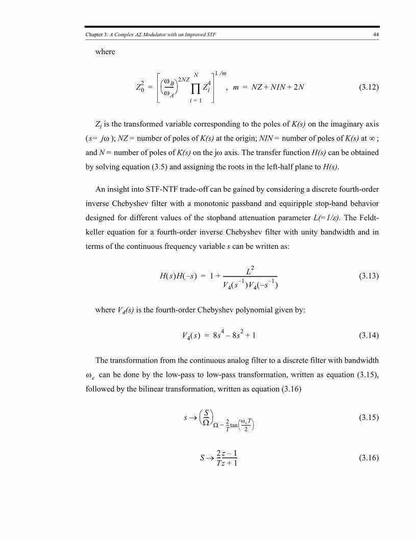
Chapter 3: A Complex ΔΣ Modulator with an Improved STF 44
where
Z02 ωB
ωA-------⎝ ⎠
⎛ ⎞2NZ
Zi4
i 1=
N
∏1 m⁄
m, NZ NIN 2N+ += = (3.12)
Zi is the transformed variable corresponding to the poles of K(s) on the imaginary axis
(s jω= ); NZ = number of poles of K(s) at the origin; NIN = number of poles of K(s) at ∞ ;
and N = number of poles of K(s) on the jω axis. The transfer function H(s) can be obtained
by solving equation (3.5) and assigning the roots in the left-half plane to H(s).
An insight into STF-NTF trade-off can be gained by considering a discrete fourth-order
inverse Chebyshev filter with a monotonic passband and equiripple stop-band behavior
designed for different values of the stopband attenuation parameter L(=1/ε). The Feldt-
keller equation for a fourth-order inverse Chebyshev filter with unity bandwidth and in
terms of the continuous frequency variable s can be written as:
H s( )H s–( ) 1 L2
V4 s 1–( )V4 s 1––( )----------------------------------------+= (3.13)
where V4(s) is the fourth-order Chebyshev polynomial given by:
V4 s( ) 8s4 8s2– 1+= (3.14)
The transformation from the continuous analog filter to a discrete filter with bandwidth
ωc can be done by the low-pass to low-pass transformation, written as equation (3.15),
followed by the bilinear transformation, written as equation (3.16)
s SΩ----⎝ ⎠
⎛ ⎞Ω 2
T--- ωcT
2---------⎝ ⎠
⎛ ⎞tan=→
S 2T--- z 1–
z 1+-----------→
(3.15)
(3.16)
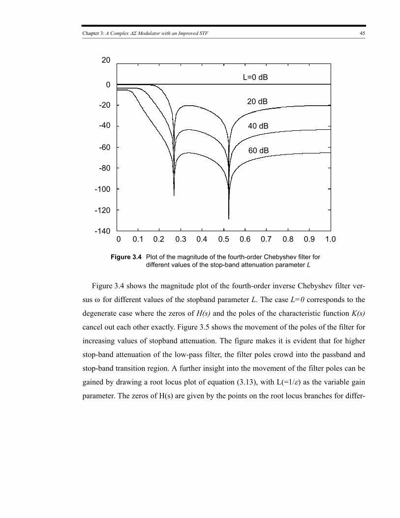
Chapter 3: A Complex ΔΣ Modulator with an Improved STF 45
20
0
-20
-40
-60
-80
-100
-120
-1400 0.1 0.2 0.3 0.4 0.5 0.6 0.7 0.8 0.9 1.0
L=0 dB
20 dB
40 dB
60 dB
Figure 3.4 Plot of the magnitude of the fourth-order Chebyshev filter for different values of the stop-band attenuation parameter L
Figure 3.4 shows the magnitude plot of the fourth-order inverse Chebyshev filter ver-
sus ω for different values of the stopband parameter L. The case L=0 corresponds to the
degenerate case where the zeros of H(s) and the poles of the characteristic function K(s)
cancel out each other exactly. Figure 3.5 shows the movement of the poles of the filter for
increasing values of stopband attenuation. The figure makes it is evident that for higher
stop-band attenuation of the low-pass filter, the filter poles crowd into the passband and
stop-band transition region. A further insight into the movement of the filter poles can be
gained by drawing a root locus plot of equation (3.13), with L(=1/ε) as the variable gain
parameter. The zeros of H(s) are given by the points on the root locus branches for differ-
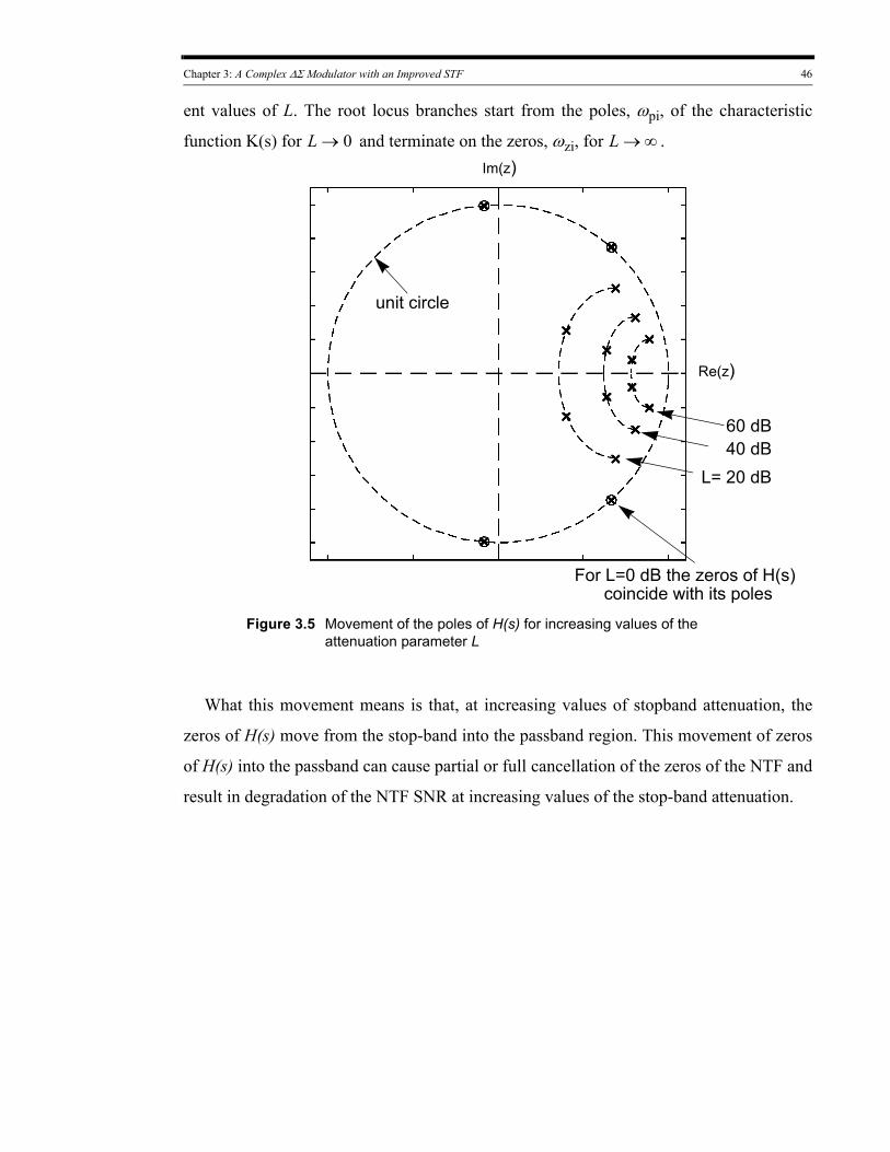
Chapter 3: A Complex ΔΣ Modulator with an Improved STF 46
ent values of L. The root locus branches start from the poles, ωpi, of the characteristic
function K(s) for L 0→ and terminate on the zeros, ωzi, for L ∞→ .
For L=0 dB the zeros of H(s)
L= 20 dB40 dB60 dB
coincide with its poles
Figure 3.5 Movement of the poles of H(s) for increasing values of the attenuation parameter L
Im(z)
Re(z)
unit circle
What this movement means is that, at increasing values of stopband attenuation, the
zeros of H(s) move from the stop-band into the passband region. This movement of zeros
of H(s) into the passband can cause partial or full cancellation of the zeros of the NTF and
result in degradation of the NTF SNR at increasing values of the stop-band attenuation.
Chapter 3: A Complex ΔΣ Modulator with an Improved STF 47
Figure 3.6 Root-locus of the equation (3.8) as the filter attenuation, L, varies
L 0→L 0→
L 0→L 0→
L ∞→
Real axis
2
-2
1
-1
0
-2 -1 0 21
Unit circle
z-plane
Imag
inar
y ax
is
3.3 Background
3.3.1 The L 1 Norm and its Impact on the NTF Poles
The L 1 norm of an impulse response of a transfer function H(z) is given by:
L 1 h n( )
n 0=
∞
∑= (3.17)
where h(n) is the impulse response of the transfer function H(z).The L 1 norm has
been used as a stability criterion in the design of delta-sigma modulators. Some of the
other criteria used in the design of stable delta-sigma modulators are:
L 2 h n( ) 2
n 0=
∞
∑= (3.18)
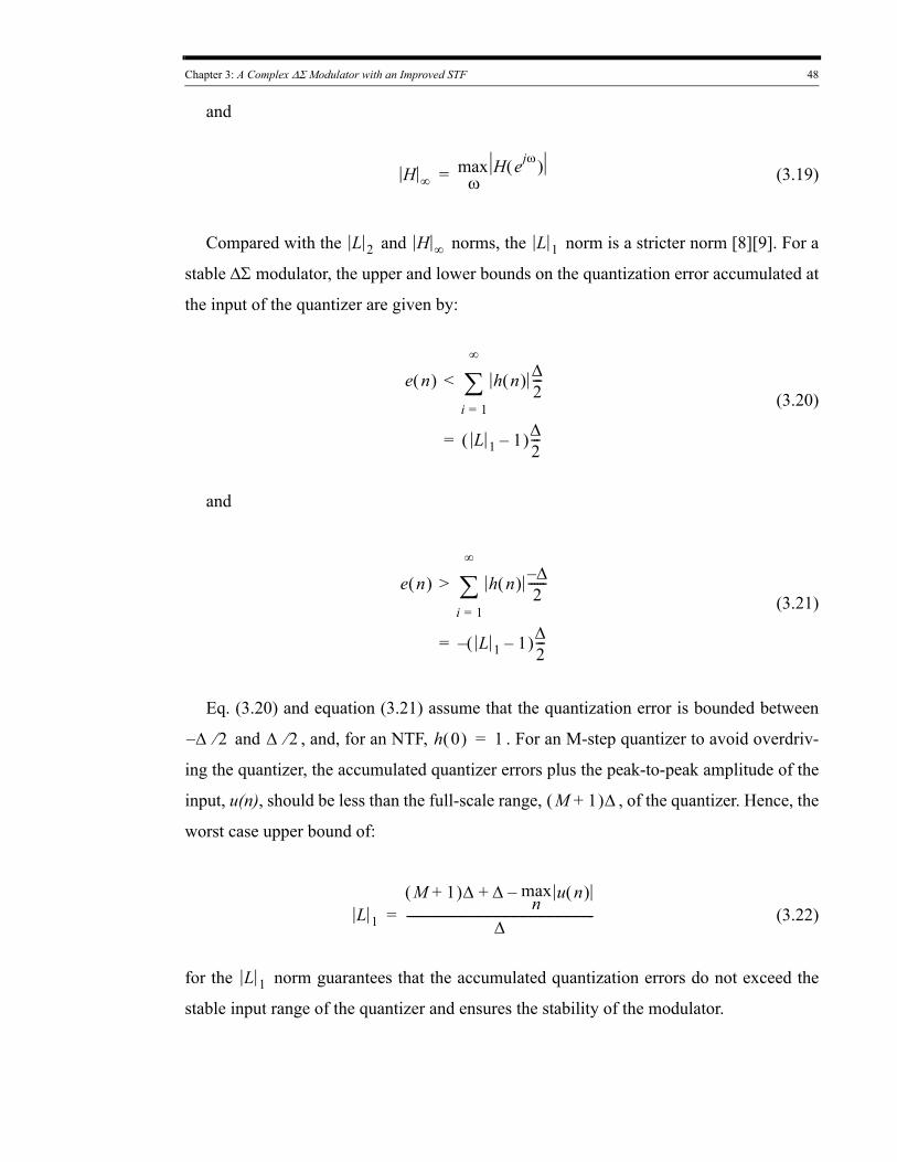
Chapter 3: A Complex ΔΣ Modulator with an Improved STF 48
and
H ∞max H ejω( )
ω= (3.19)
Compared with the L 2 and H ∞ norms, the L 1 norm is a stricter norm [8][9]. For a
stable ΔΣ modulator, the upper and lower bounds on the quantization error accumulated at
the input of the quantizer are given by:
e n( ) < h n( ) Δ2---
i 1=
∞
∑
= L 1 1–( )Δ2---
(3.20)
and
e n( ) > h n( ) Δ–2
------i 1=
∞
∑
= L 1 1–( )– Δ2---
(3.21)
Eq. (3.20) and equation (3.21) assume that the quantization error is bounded between
Δ 2⁄– and Δ 2⁄ , and, for an NTF, h 0( ) 1= . For an M-step quantizer to avoid overdriv-
ing the quantizer, the accumulated quantizer errors plus the peak-to-peak amplitude of the
input, u(n), should be less than the full-scale range, M 1+( )Δ , of the quantizer. Hence, the
worst case upper bound of:
L 1
M 1+( )Δ Δ maxn u n( )–+
Δ----------------------------------------------------------------= (3.22)
for the L 1 norm guarantees that the accumulated quantization errors do not exceed the
stable input range of the quantizer and ensures the stability of the modulator.
Chapter 3: A Complex ΔΣ Modulator with an Improved STF 49
.
Figure 3.7 (a) NTF magnitude for different values of the |L|1 norm, (b) movement of the NTF poles with an increase in the |L|1 norm
Normalized frequency (
20
-60
0
-40
-20
0 0.1 0.30.2
Mag
nitu
de R
espo
nse
(dB
)
-80
-100
0.4 0.5
L 1 8=
1 fs→ )
45
3
-120
-140
Im(z)
Re(z)
L 1 8=5
43
(a)
(b)
The relation of the L 1 norm to the NTF gain and the poles of the NTF can be seen in
Figure 3.7. Figure 3.7(a) shows the magnitude response for a fourth-order NTF at differ-
ent values of the L 1 norm. The NTF poles have been designed using the inverse Cheby-
shev function from the Matlab toolbox [10], and the NTF zeros have been independently
Chapter 3: A Complex ΔΣ Modulator with an Improved STF 50
distributed over the signal bandwidth. Figure 3.7(a) shows a pole-zero plot of the NTF
poles and the corresponding values of the L 1 norm. From Figure 3.7, the conclusion may
be drawn that the L 1 norm increases as the NTF poles move away from the signal pass-
band. This relation of L 1 norm to the NTF poles can be used to constrain the placement
of the NTF poles and hence indirectly control the STF stop-band attenuation. This relation
forms one of the constraints in the STF-NTF design optimization algorithm.
3.3.2 The Loss Function L(Z)
As discussed in section 3.2, the poles of the characteristic function K(s) are constrained
to be in the stop-band region, and the zeros are constrained to be in the passband region.
By defining the poles of K(s) and the type of desired passband, it is possible to use simple
formulae, as shown in equation (3.9) and equation (3.10), to directly calculate the zeros of
the characteristic function K(s). These calculated zeros and the pre-defined poles can then
be used in solving the Feldtkeller’s equation and extracting the zeros of the input-output
transfer function H(s).
The approximation problem for filter design when the zeros of the filter and the desired
passband response are defined can be solved by a computer program illustrated in the
flowchart of Figure 3.8. This solution means that, given the filter zeros, the passband devi-
ation, and the passband type the filter transfer function can be determined. However, in
actual filter design, the stopband zeros are not known, and the task of the computer pro-
gram still remains to find them. It is possible to introduce a function, L(Z), which, for an
equiripple or maximally flat passband type, enables us to calculate the stop-band attenua-
tion only in the terms of filter zeros. For a filter with an equiripple filter passband
ωA ω ωB≤ ≤ and with the following zeros:
• NZ zeros at the origin
• N finite zeros at ωi (i=1,2,…N )
• NIN zeros at infinity
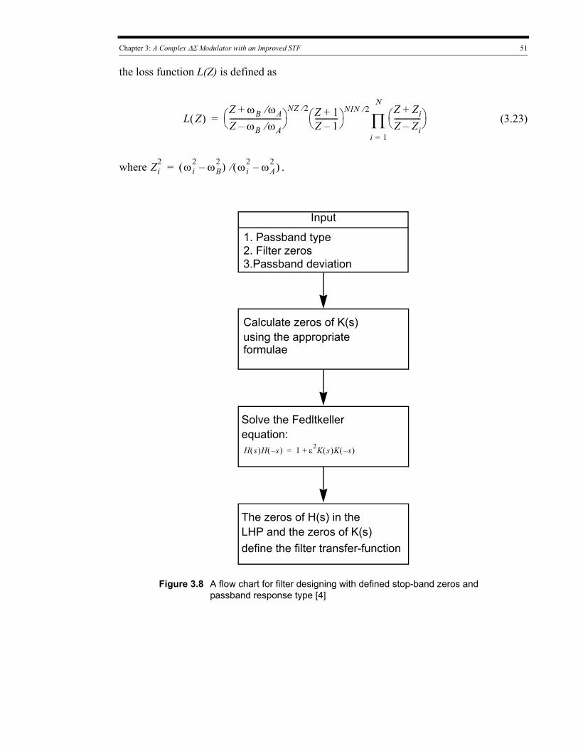
Chapter 3: A Complex ΔΣ Modulator with an Improved STF 51
the loss function L(Z) is defined as
L Z( )Z ωB ωA⁄+Z ωB ωA⁄–---------------------------⎝ ⎠
⎛ ⎞NZ 2⁄ Z 1+
Z 1–------------⎝ ⎠
⎛ ⎞ NIN 2⁄ Z Zi+Z Zi–--------------⎝ ⎠
⎛ ⎞
i 1=
N
∏= (3.23)
where Zi2 ωi
2 ωB2–( ) ωi
2 ωA2–( )⁄= .
Figure 3.8 A flow chart for filter designing with defined stop-band zeros and passband response type [4]
Input
1. Passband type2. Filter zeros3.Passband deviation
Calculate zeros of K(s)using the appropriate formulae
Solve the Fedltkeller equation: H s( )H s–( ) 1 ε2K s( )K s–( )+=
The zeros of H(s) in the LHP and the zeros of K(s)define the filter transfer-function
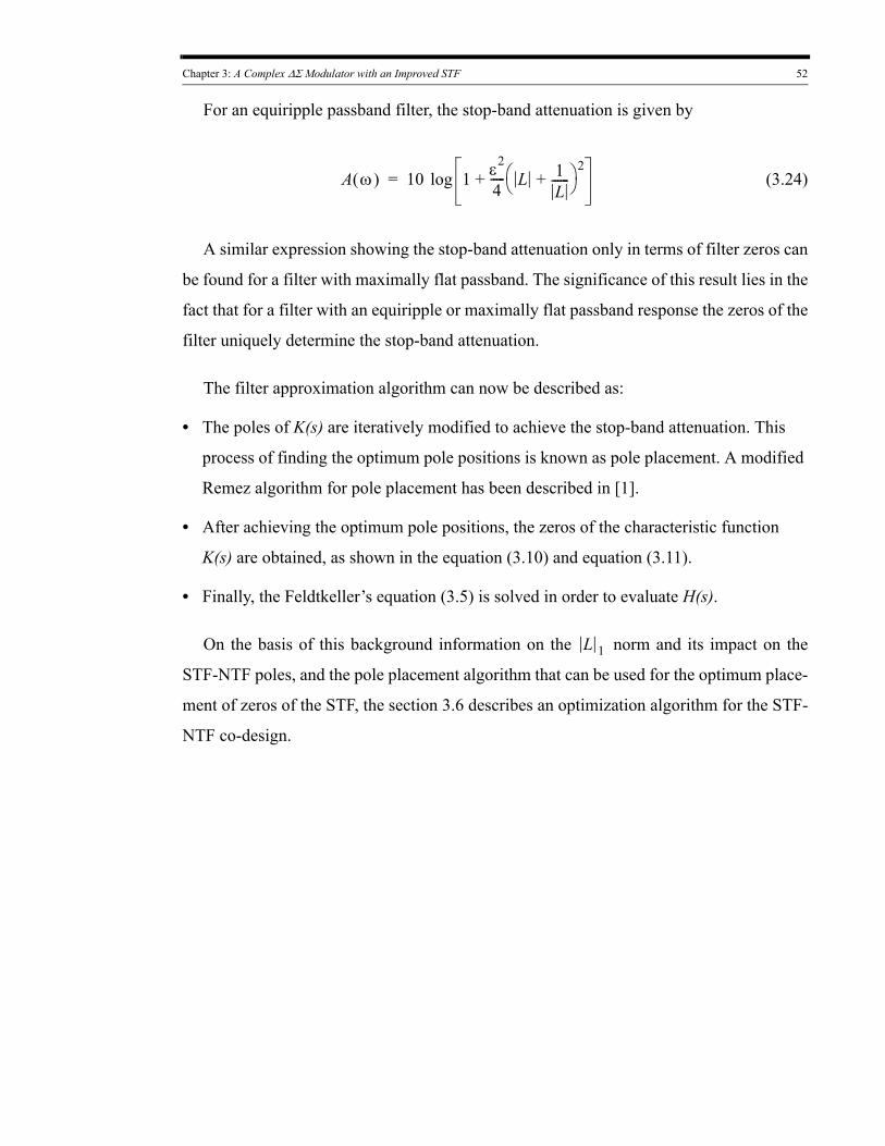
Chapter 3: A Complex ΔΣ Modulator with an Improved STF 52
For an equiripple passband filter, the stop-band attenuation is given by
A ω( ) 10 1 ε2
4----- L 1
L------+⎝ ⎠
⎛ ⎞ 2+log= (3.24)
A similar expression showing the stop-band attenuation only in terms of filter zeros can
be found for a filter with maximally flat passband. The significance of this result lies in the
fact that for a filter with an equiripple or maximally flat passband response the zeros of the
filter uniquely determine the stop-band attenuation.
The filter approximation algorithm can now be described as:
• The poles of K(s) are iteratively modified to achieve the stop-band attenuation. This
process of finding the optimum pole positions is known as pole placement. A modified
Remez algorithm for pole placement has been described in [1].
• After achieving the optimum pole positions, the zeros of the characteristic function
K(s) are obtained, as shown in the equation (3.10) and equation (3.11).
• Finally, the Feldtkeller’s equation (3.5) is solved in order to evaluate H(s).
On the basis of this background information on the L 1 norm and its impact on the
STF-NTF poles, and the pole placement algorithm that can be used for the optimum place-
ment of zeros of the STF, the section 3.6 describes an optimization algorithm for the STF-
NTF co-design.
Chapter 3: A Complex ΔΣ Modulator with an Improved STF 53
3.4 STF-NTF Co-Design Optimization Algorithm for the Design of Real ΔΣ Modulators
The STF-NTF co-design optimization algorithm for the design of lowpass ΔΣ modula-
tor transfer functions can be described as [5]:
• The zeros of the STF are derived using the pole-placement algorithm described in [1].;
• The Optimization algorithm proceeds with the minimization of the objective function,
given by:
NTF ω( ) 2 ωd0
ωs
2OSR---------------
∫ (3.25)
Note the limits of the integral have been modified to correspond to the in-band noise
for the lowpass case.
• The constraints for the minimization of the objective function are
(a) the L 1 norm of the impulse response of the NTF.
(b) the maximum radius for the NTF poles.
(c) the maximum-deviation of the STF over the passband
An additional constraint on the complex poles and zeros of the NTF and STF is that
they occur in complex conjugates. This limitation restricts the flexibility to place the com-
plex poles and zeros in optimal positions:
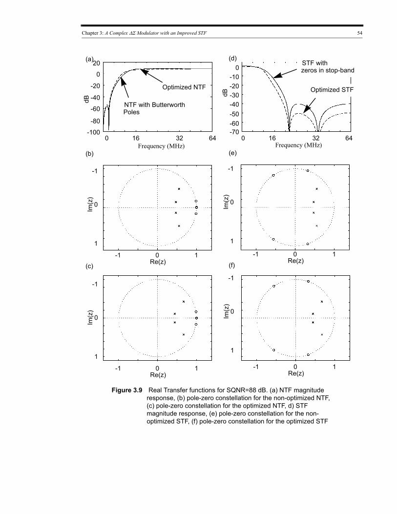
Chapter 3: A Complex ΔΣ Modulator with an Improved STF 54
Figure 3.9 Real Transfer functions for SQNR=88 dB. (a) NTF magnitude response, (b) pole-zero constellation for the non-optimized NTF, (c) pole-zero constellation for the optimized NTF, d) STF magnitude response, (e) pole-zero constellation for the non-optimized STF, (f) pole-zero constellation for the optimized STF
6416 32-100
-80
-60
-40
-20
0
20
0
-60-50-40-30-20-10
0
Frequency (MHz) Frequency (MHz)
dB
dB
1-1 0
1
-1
0
Re(z)
Im(z
)
1-1 0
1
-1
0
Re(z)
Im(z
)
1-1 0
1
-1
0
Re(z)
Im(z
)
1-1 0
1
-1
0
Re(z)
Im(z
)
-706416 320
zeros in stop-bandSTF with
Optimized STF
PolesNTF with Butterworth
Optimized NTF
(a) (d)
(b) (e)
(c) (f)
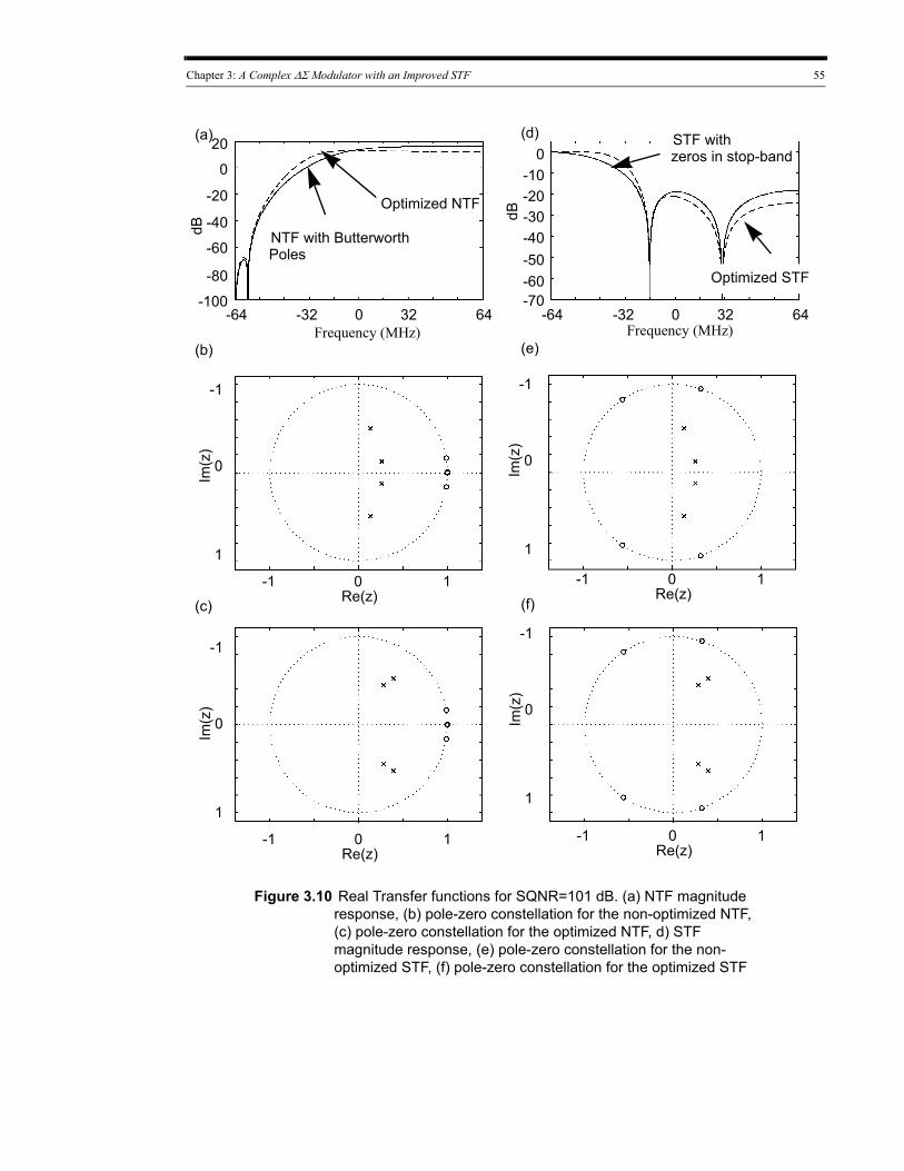
Chapter 3: A Complex ΔΣ Modulator with an Improved STF 55
Figure 3.10 Real Transfer functions for SQNR=101 dB. (a) NTF magnitude response, (b) pole-zero constellation for the non-optimized NTF, (c) pole-zero constellation for the optimized NTF, d) STF magnitude response, (e) pole-zero constellation for the non-optimized STF, (f) pole-zero constellation for the optimized STF
64-32 0 32-100
-80
-60
-40
-20
0
20
-64 64-32 0 32
-60-50-40-30-20-10
0
-64Frequency (MHz) Frequency (MHz)
dB
dB
1-1 0
1
-1
0
Re(z)
Im(z
)
1-1 0
1
-1
0
Re(z)
Im(z
)
1-1 0
1
-1
0
Re(z)
Im(z
)
1-1 0
1
-1
0
Re(z)
Im(z
)
-70
zeros in stop-bandSTF with
Optimized STFPolesNTF with Butterworth
Optimized NTF
(a) (d)
(b) (e)
(c) (f)
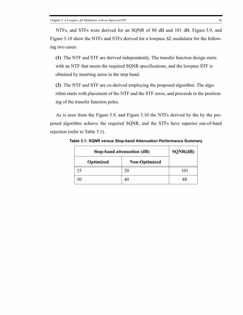
Chapter 3: A Complex ΔΣ Modulator with an Improved STF 56
NTFs, and STFs were derived for an SQNR of 88 dB and 101 dB. Figure 3.9, and
Figure 3.10 show the NTFs and STFs derived for a lowpass ΔΣ modulator for the follow-
ing two cases:
(1) The NTF and STF are derived independently. The transfer function design starts
with an NTF that meets the required SQNR specifications, and the lowpass STF is
obtained by inserting zeros in the stop band,
(2) The NTF and STF are co-derived employing the proposed algorithm. The algo-
rithm starts with placement of the NTF and the STF zeros, and proceeds to the position-
ing of the transfer function poles.
As is seen from the Figure 3.9, and Figure 3.10 the NTFs derived by the by the pro-
posed algorithm achieve the required SQNR, and the STFs have superior out-of-band
rejection (refer to Table 3.1).
Table 3.1: SQNR versus Stop-band Attenuation Performance Summary
Stop-band attenuation (dB) SQNR(dB)
Optimized Non-Optimized
25 20 101
50 40 88
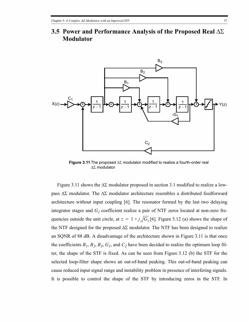
Chapter 3: A Complex ΔΣ Modulator with an Improved STF 57
3.5 Power and Performance Analysis of the Proposed Real ΔΣ Modulator
B1
B2
1z 1–------------ 1
z 1–------------
C2
C1X(z) 1
z 1–------------ 1
z 1–------------
Figure 3.11 The proposed ΔΣ modulator modified to realize a fourth-order real ΔΣ modulator
++++ Y(z)
B3
-G1
+
Figure 3.11 shows the ΔΣ modulator proposed in section 3.1 modified to realize a low-
pass ΔΣ modulator. The ΔΣ modulator architecture resembles a distributed feedforward
architecture without input coupling [6]. The resonator formed by the last two delaying
integrator stages and G1 coefficient realize a pair of NTF zeros located at non-zero fre-
quencies outside the unit circle, at z 1 j G1+= [6]. Figure 3.12 (a) shows the shape of
the NTF designed for the proposed ΔΣ modulator. The NTF has been designed to realize
an SQNR of 88 dB. A disadvantage of the architecture shown in Figure 3.11 is that once
the coefficients B1, B2, B3, G1, and C2 have been decided to realize the optimum loop fil-
ter, the shape of the STF is fixed. As can be seen from Figure 3.12 (b) the STF for the
selected loop-filter shape shows an out-of-band peaking. This out-of-band peaking can
cause reduced input signal range and instability problem in presence of interfering signals.
It is possible to control the shape of the STF by introducing zeros in the STF. In
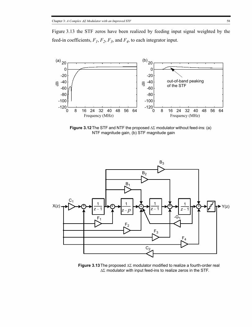
Chapter 3: A Complex ΔΣ Modulator with an Improved STF 58
Figure 3.13 the STF zeros have been realized by feeding input signal weighted by the
feed-in coefficients, F1, F2, F3, and F4, to each integrator input.
-120-100
-80-60-40-20
0
320 16Frequency (MHz)
8 24
20
64564840
dB
-120-100
-80-60-40-20
0
320 16Frequency (MHz)
8 24
20
64564840
dB
Figure 3.12The STF and NTF the proposed ΔΣ modulator without feed-ins: (a) NTF magnitude gain, (b) STF magnitude gain
out-of-band peaking of the STF
(a) (b)
F3
F2
F1
B1
B2
1z 1–------------ 1
z p–-------------
C2
C1X(z) 1
z 1–------------ 1
z 1–------------
Figure 3.13The proposed ΔΣ modulator modified to realize a fourth-order real ΔΣ modulator with input feed-ins to realize zeros in the STF.
++++ Y(z)
B3
F4
-G1
+
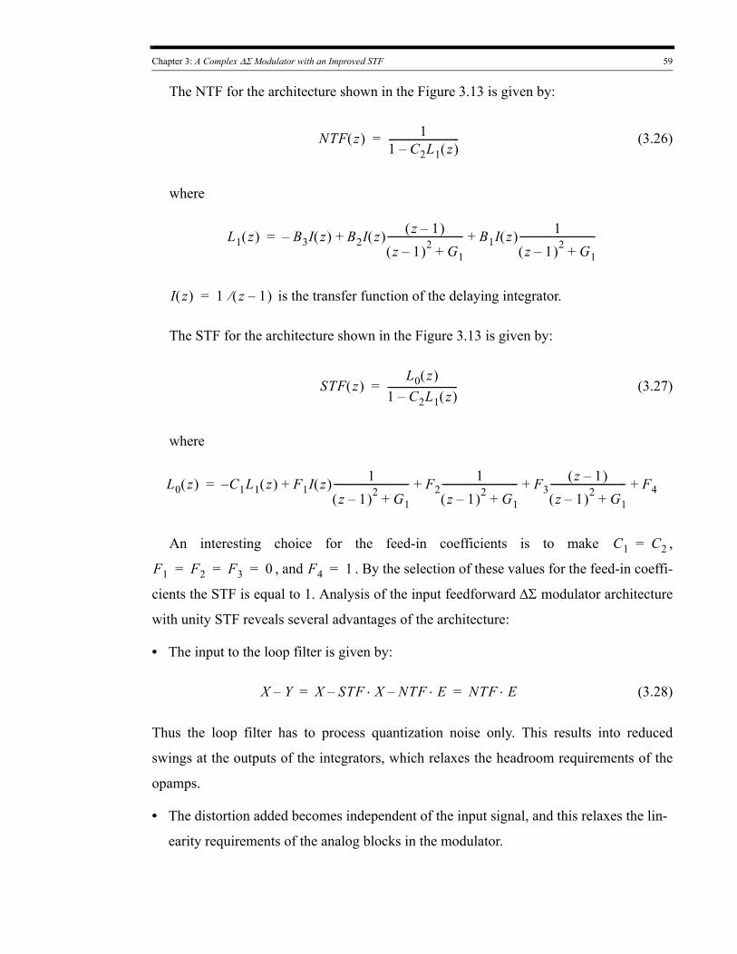
Chapter 3: A Complex ΔΣ Modulator with an Improved STF 59
The NTF for the architecture shown in the Figure 3.13 is given by:
NTF z( ) 11 C2L1 z( )–-----------------------------= (3.26)
where
L1 z( ) B3I z( )– B2I z( ) z 1–( )
z 1–( )2 G1+------------------------------- B1I z( ) 1
z 1–( )2 G1+-------------------------------+ +=
I z( ) 1 z 1–( )⁄= is the transfer function of the delaying integrator.
The STF for the architecture shown in the Figure 3.13 is given by:
STF z( )L0 z( )
1 C2L1 z( )–-----------------------------= (3.27)
where
L0 z( ) C– 1L1 z( ) F1I z( ) 1z 1–( )2 G1+
------------------------------- F21
z 1–( )2 G1+------------------------------- F3
z 1–( )
z 1–( )2 G1+------------------------------- F4+ + + +=
An interesting choice for the feed-in coefficients is to make C1 C2= ,
F1 F2 F3 0= = = , and F4 1= . By the selection of these values for the feed-in coeffi-
cients the STF is equal to 1. Analysis of the input feedforward ΔΣ modulator architecture
with unity STF reveals several advantages of the architecture:
• The input to the loop filter is given by:
X Y– X STF X NTF E⋅–⋅– NTF E⋅= = (3.28)
Thus the loop filter has to process quantization noise only. This results into reduced
swings at the outputs of the integrators, which relaxes the headroom requirements of the
opamps.
• The distortion added becomes independent of the input signal, and this relaxes the lin-
earity requirements of the analog blocks in the modulator.
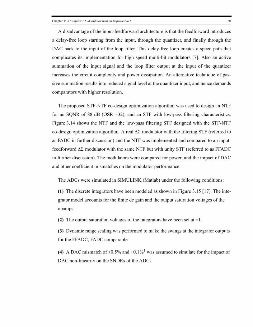
Chapter 3: A Complex ΔΣ Modulator with an Improved STF 60
A disadvantage of the input-feedforward architecture is that the feedforward introduces
a delay-free loop starting from the input, through the quantizer, and finally through the
DAC back to the input of the loop filter. This delay-free loop creates a speed path that
complicates its implementation for high speed multi-bit modulators [7]. Also an active
summation of the input signal and the loop filter output at the input of the quantizer
increases the circuit complexity and power dissipation. An alternative technique of pas-
sive summation results into reduced signal level at the quantizer input, and hence demands
comparators with higher resolution.
The proposed STF-NTF co-design optimization algorithm was used to design an NTF
for an SQNR of 88 dB (OSR =32), and an STF with low-pass filtering characteristics.
Figure 3.14 shows the NTF and the low-pass filtering STF designed with the STF-NTF
co-design optimization algorithm. A real ΔΣ modulator with the filtering STF (referred to
as FADC in further discussion) and the NTF was implemented and compared to an input-
feedforward ΔΣ modulator with the same NTF but with unity STF (referred to as FFADC
in further discussion). The modulators were compared for power, and the impact of DAC
and other coefficient mismatches on the modulator performance.
The ADCs were simulated in SIMULINK (Matlab) under the following conditions:
(1) The discrete integrators have been modeled as shown in Figure 3.15 [17]. The inte-
grator model accounts for the finite dc gain and the output saturation voltages of the
opamps.
(2) The output saturation voltages of the integrators have been set at ±1.
(3) Dynamic range scaling was performed to make the swings at the integrator outputs
for the FFADC, FADC comparable.
(4) A DAC mismatch of ±0.5% and ±0.1%1 was assumed to simulate for the impact of
DAC non-linearity on the SNDRs of the ADCs.
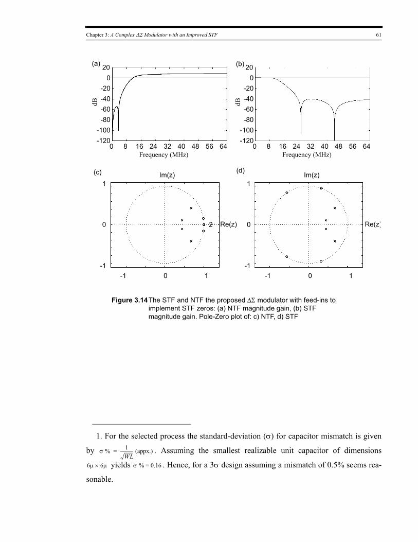
Chapter 3: A Complex ΔΣ Modulator with an Improved STF 61
-120-100
-80-60-40-20
0
320 16Frequency (MHz)
8 24
20
64564840
dB
-120-100
-80-60-40-20
0
320 16Frequency (MHz)
8 24
20
64564840
dB
Figure 3.14The STF and NTF the proposed ΔΣ modulator with feed-ins to implement STF zeros: (a) NTF magnitude gain, (b) STF magnitude gain. Pole-Zero plot of: c) NTF, d) STF
2
1-1-1
1
0
0
Im(z)
Re(z)
1-1-1
1
0
0
Im(z)
Re(z)
(a) (b)
(c) (d)
1. For the selected process the standard-deviation (σ) for capacitor mismatch is given
by σ % 1WL
------------ (appx.)= . Assuming the smallest realizable unit capacitor of dimensions
6μ 6μ× yields σ % = 0.16 . Hence, for a 3σ design assuming a mismatch of 0.5% seems rea-
sonable.
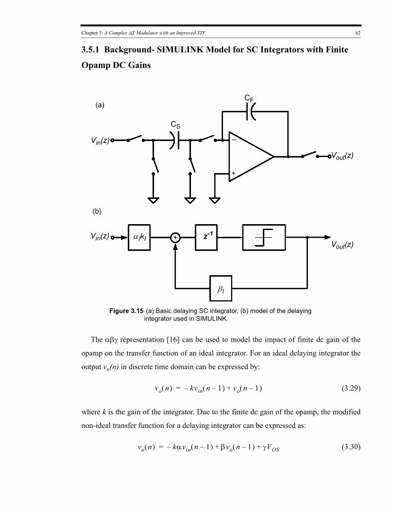
Chapter 3: A Complex ΔΣ Modulator with an Improved STF 62
3.5.1 Background- SIMULINK Model for SC Integrators with Finite
Opamp DC Gains
Figure 3.15 (a) Basic delaying SC integrator, (b) model of the delaying integrator used in SIMULINK.
z-1Vin(z)Vout(z)
CF
CS
Vin(z)
Vout(z)
–
+
βI
αΙkI +
(a)
(b)
The αβγ representation [16] can be used to model the impact of finite dc gain of the
opamp on the transfer function of an ideal integrator. For an ideal delaying integrator the
output vo(n) in discrete time domain can be expressed by:
vo n( ) kvin n 1–( )– vo n 1–( )+= (3.29)
where k is the gain of the integrator. Due to the finite dc gain of the opamp, the modified
non-ideal transfer function for a delaying integrator can be expressed as:
vo n( ) kαvin n 1–( )– βvo n 1–( ) γVOS+ += (3.30)
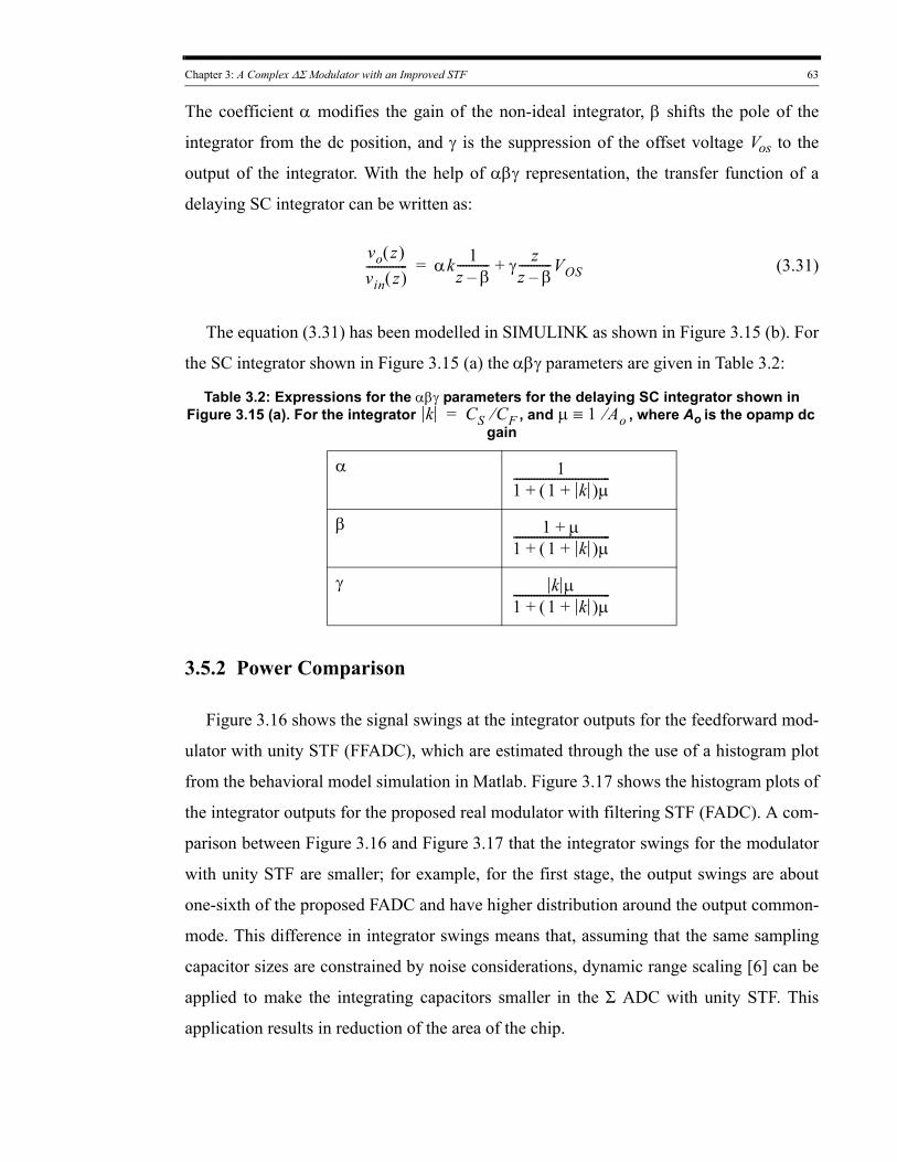
Chapter 3: A Complex ΔΣ Modulator with an Improved STF 63
The coefficient α modifies the gain of the non-ideal integrator, β shifts the pole of the
integrator from the dc position, and γ is the suppression of the offset voltage Vos to the
output of the integrator. With the help of αβγ representation, the transfer function of a
delaying SC integrator can be written as:
vo z( )vin z( )-------------- αk 1
z β–----------- γ z
z β–-----------VOS+= (3.31)
The equation (3.31) has been modelled in SIMULINK as shown in Figure 3.15 (b). For
the SC integrator shown in Figure 3.15 (a) the αβγ parameters are given in Table 3.2:
Table 3.2: Expressions for the αβγ parameters for the delaying SC integrator shown in Figure 3.15 (a). For the integrator k CS CF⁄= , and μ 1 Ao⁄≡ , where Ao is the opamp dc
gain
α 11 1 k+( )μ+---------------------------------
β 1 μ+1 1 k+( )μ+---------------------------------
γ k μ1 1 k+( )μ+---------------------------------
3.5.2 Power Comparison
Figure 3.16 shows the signal swings at the integrator outputs for the feedforward mod-
ulator with unity STF (FFADC), which are estimated through the use of a histogram plot
from the behavioral model simulation in Matlab. Figure 3.17 shows the histogram plots of
the integrator outputs for the proposed real modulator with filtering STF (FADC). A com-
parison between Figure 3.16 and Figure 3.17 that the integrator swings for the modulator
with unity STF are smaller; for example, for the first stage, the output swings are about
one-sixth of the proposed FADC and have higher distribution around the output common-
mode. This difference in integrator swings means that, assuming that the same sampling
capacitor sizes are constrained by noise considerations, dynamic range scaling [6] can be
applied to make the integrating capacitors smaller in the Σ ADC with unity STF. This
application results in reduction of the area of the chip.
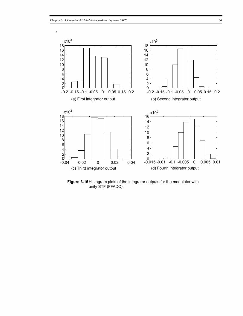
Chapter 3: A Complex ΔΣ Modulator with an Improved STF 64
.
-0.05 0.05 0.150-0.1
x103 x103
x103
141210
68
24
x103
-0.1 0-0.005-0.01 0.005 0.01-0.015
18
14
10
0.2-0.15-0.2
0.020-0.02 0.04-0.04
Figure 3.16Histogram plots of the integrator outputs for the modulator with unity STF (FFADC).
(a) First integrator output (b) Second integrator output
(c) Third integrator output (d) Fourth integrator output
0
6
16
12
8
24
0
18
14
10
6
16
12
8
24
0
18
14
10
6
16
12
8
24
0-0.05 0.05 0.150-0.1 0.2-0.15-0.2
16
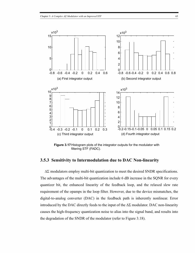
Chapter 3: A Complex ΔΣ Modulator with an Improved STF 65
-0.2 0.2 0.40-0.4
x103 x103
8765
34
12
x103
910 14
1210
68
24
x103
-0.1 0-0.05-0.15 0.05 0.1 0.15 0.2-0.2
15
10
5
0.6-0.6-0.8 -0.2 0.2 0.40-0.4
12
10
8
4
6
0
2
0.6-0.6-0.8 0.8
-0.1 0.1 0.20-0.2 0.3-0.3-0.4
Figure 3.17Histogram plots of the integrator outputs for the modulator with filtering STF (FADC).
(a) First integrator output (b) Second integrator output
(c) Third integrator output (d) Fourth integrator output
0 0
0
3.5.3 Sensitivity to Intermodulation due to DAC Non-linearity
ΔΣ modulators employ multi-bit quantization to meet the desired SNDR specifications.
The advantages of the multi-bit quantization include 6 dB increase in the SQNR for every
quantizer bit, the enhanced linearity of the feedback loop, and the relaxed slew rate
requirement of the opamps in the loop filter. However, due to the device mismatches, the
digital-to-analog converter (DAC) in the feedback path is inherently nonlinear. Error
introduced by the DAC directly feeds to the input of the ΔΣ modulator. DAC non-linearity
causes the high-frequency quantization noise to alias into the signal band, and results into
the degradation of the SNDR of the modulator (refer to Figure 3.18).
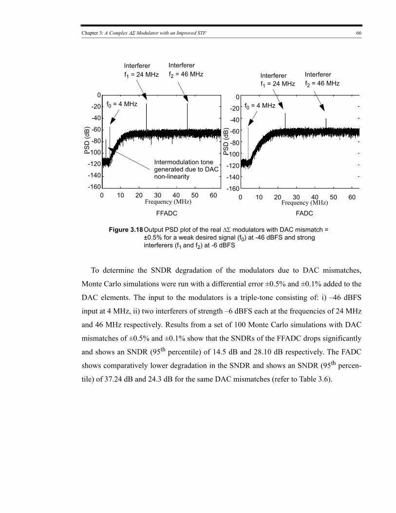
Chapter 3: A Complex ΔΣ Modulator with an Improved STF 66
PS
D (d
B)
30 50 604020
-60
-80
-100
-140
-120
-160100
FADC
0
-20
-40
30 50 604020
-60
-80
-100
-140
-120
-160100
0
-20
-40
PS
D (d
B)
FFADC
Figure 3.18Output PSD plot of the real ΔΣ modulators with DAC mismatch = ±0.5% for a weak desired signal (f0) at -46 dBFS and strong interferers (f1 and f2) at -6 dBFS
Intermodulation tonegenerated due to DACnon-linearity
Frequency (MHz) Frequency (MHz)
Interfererf1 = 24 MHz
Interfererf2 = 46 MHz
f0 = 4 MHz
f1 = 24 MHzInterfererf2 = 46 MHz
f0 = 4 MHz
Interferer
To determine the SNDR degradation of the modulators due to DAC mismatches,
Monte Carlo simulations were run with a differential error ±0.5% and ±0.1% added to the
DAC elements. The input to the modulators is a triple-tone consisting of: i) –46 dBFS
input at 4 MHz, ii) two interferers of strength –6 dBFS each at the frequencies of 24 MHz
and 46 MHz respectively. Results from a set of 100 Monte Carlo simulations with DAC
mismatches of ±0.5% and ±0.1% show that the SNDRs of the FFADC drops significantly
and shows an SNDR (95th percentile) of 14.5 dB and 28.10 dB respectively. The FADC
shows comparatively lower degradation in the SNDR and shows an SNDR (95th percen-
tile) of 37.24 dB and 24.3 dB for the same DAC mismatches (refer to Table 3.6).
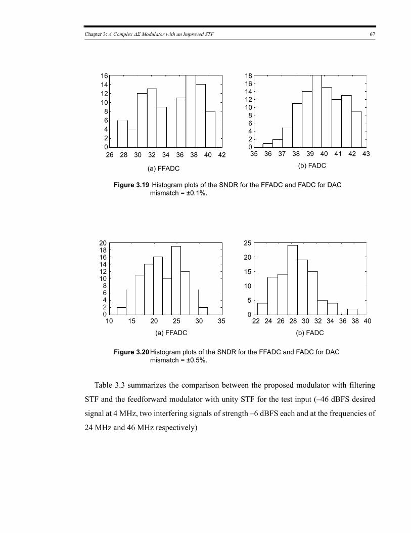
Chapter 3: A Complex ΔΣ Modulator with an Improved STF 67
32 36 383430
16
10
4
402826 38 40 413937
181614
1012
4
8
423635 43
Figure 3.19 Histogram plots of the SNDR for the FFADC and FADC for DAC mismatch = ±0.1%.
(a) FFADC (b) FADC
0
1412
86
2
42
20
6
25 353020
20
12
6
1510 28 32 343026
25
20
15
5
10
0362422 38
Figure 3.20Histogram plots of the SNDR for the FFADC and FADC for DAC mismatch = ±0.5%.
(a) FFADC (b) FADC
0
1816
108
4
14
2
40
Table 3.3 summarizes the comparison between the proposed modulator with filtering
STF and the feedforward modulator with unity STF for the test input (–46 dBFS desired
signal at 4 MHz, two interfering signals of strength –6 dBFS each and at the frequencies of
24 MHz and 46 MHz respectively)
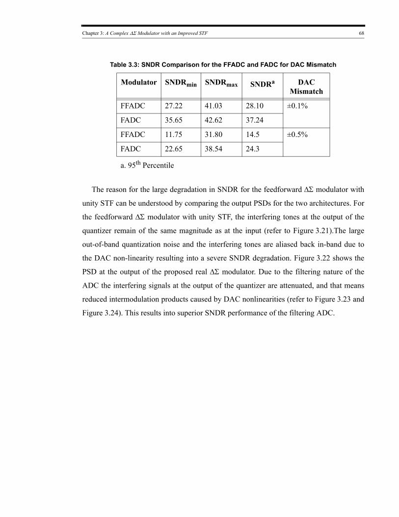
Chapter 3: A Complex ΔΣ Modulator with an Improved STF 68
Table 3.3: SNDR Comparison for the FFADC and FADC for DAC Mismatch
Modulator SNDRmin SNDRmax SNDRa DAC Mismatch
FFADC 27.22 41.03 28.10 ±0.1%
FADC 35.65 42.62 37.24
FFADC 11.75 31.80 14.5 ±0.5%
FADC 22.65 38.54 24.3
a. 95th Percentile
The reason for the large degradation in SNDR for the feedforward ΔΣ modulator with
unity STF can be understood by comparing the output PSDs for the two architectures. For
the feedforward ΔΣ modulator with unity STF, the interfering tones at the output of the
quantizer remain of the same magnitude as at the input (refer to Figure 3.21).The large
out-of-band quantization noise and the interfering tones are aliased back in-band due to
the DAC non-linearity resulting into a severe SNDR degradation. Figure 3.22 shows the
PSD at the output of the proposed real ΔΣ modulator. Due to the filtering nature of the
ADC the interfering signals at the output of the quantizer are attenuated, and that means
reduced intermodulation products caused by DAC nonlinearities (refer to Figure 3.23 and
Figure 3.24). This results into superior SNDR performance of the filtering ADC.
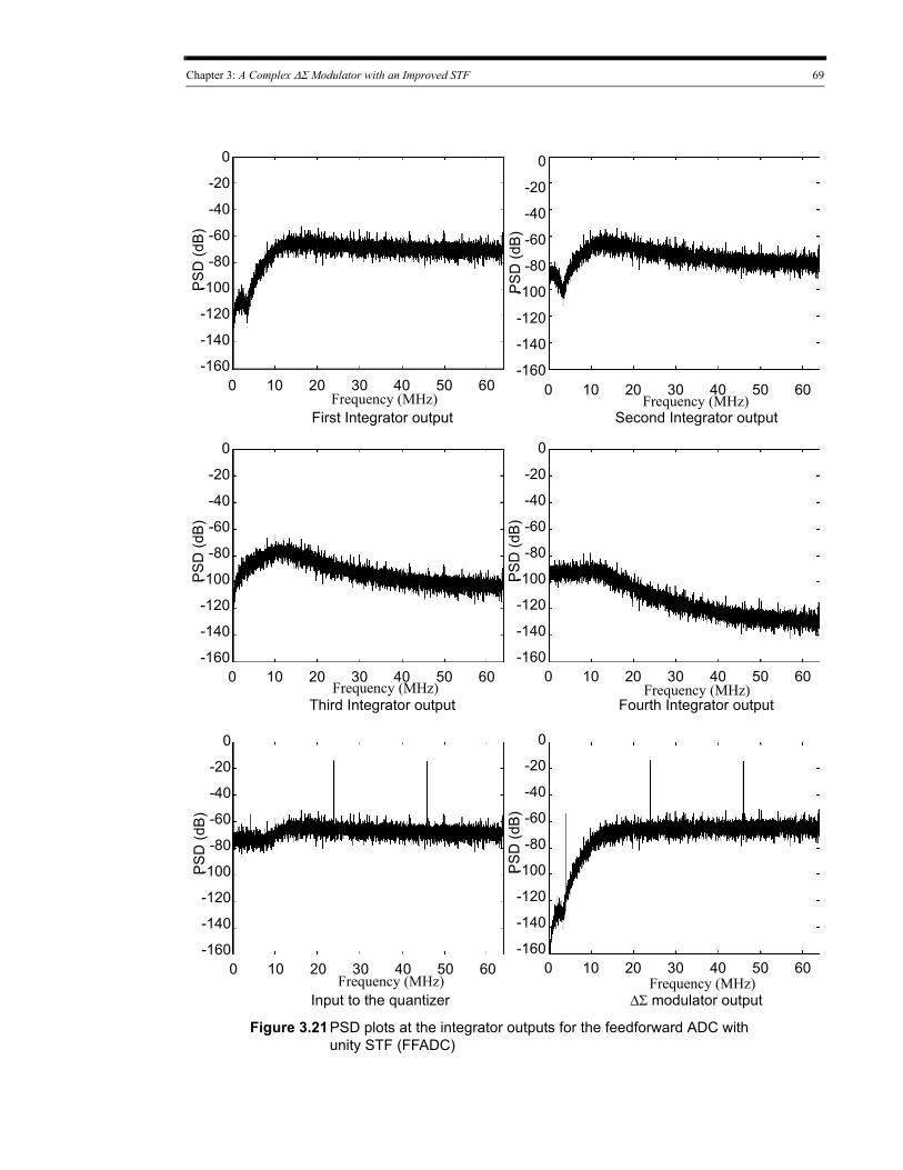
Chapter 3: A Complex ΔΣ Modulator with an Improved STF 69
Figure 3.21PSD plots at the integrator outputs for the feedforward ADC with unity STF (FFADC)
PS
D (d
B)
30 50 604020
-60
-80
-100
-140
-120
-160100
Second Integrator output
0
-20
-40
30 50 604020
-60
-80
-100
-140
-120
-160100
0
-20
-40
PS
D (d
B)
PS
D (d
B)
30 50 604020
-60
-80
-100
-140
-120
-160100
0
-20
-40P
SD
(dB
)
30 50 604020
-60
-80
-100
-140
-120
-160100
0
-20
-40P
SD
(dB
)
30 50 604020
-60
-80
-100
-140
-120
-160100
0
-20
-40
PS
D (d
B)
30 50 604020
-60
-80
-100
-140
-120
-160100
0
-20
-40
First Integrator output
Third Integrator output Fourth Integrator output
Input to the quantizer ΔΣ modulator output
Frequency (MHz) Frequency (MHz)
Frequency (MHz) Frequency (MHz)
Frequency (MHz) Frequency (MHz)
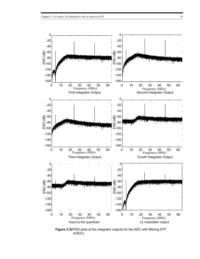
Chapter 3: A Complex ΔΣ Modulator with an Improved STF 70
Figure 3.22PSD plots at the integrator outputs for the ADC with filtering STF (FADC)
PS
D (d
B)
30 50 604020
-60
-80
-100
-140
-120
-160100
0
-20
-40P
SD
(dB
)
30 50 604020
-60
-80
-100
-140
-120
-160100
0
-20
-40
PS
D (d
B)
30 50 604020
-60
-80
-100
-140
-120
-160100
0
-20
-40
First Integrator Output
Third Integrator Output
Input to the quantizer
PS
D (d
B)
30 50 604020
-60
-80
-100
-140
-120
-160100
0
-20
-40
PS
D (d
B)
30 50 604020
-60
-80
-100
-140
-120
-160100
0
-20
-40P
SD
(dB
)
30 50 604020
-60
-80
-100
-140
-120
-160100
0
-20
-40
Second Integrator Output
Fourth Integrator Output
ΔΣ modulator output
Frequency (MHz) Frequency (MHz)
Frequency (MHz) Frequency (MHz)
Frequency (MHz) Frequency (MHz)
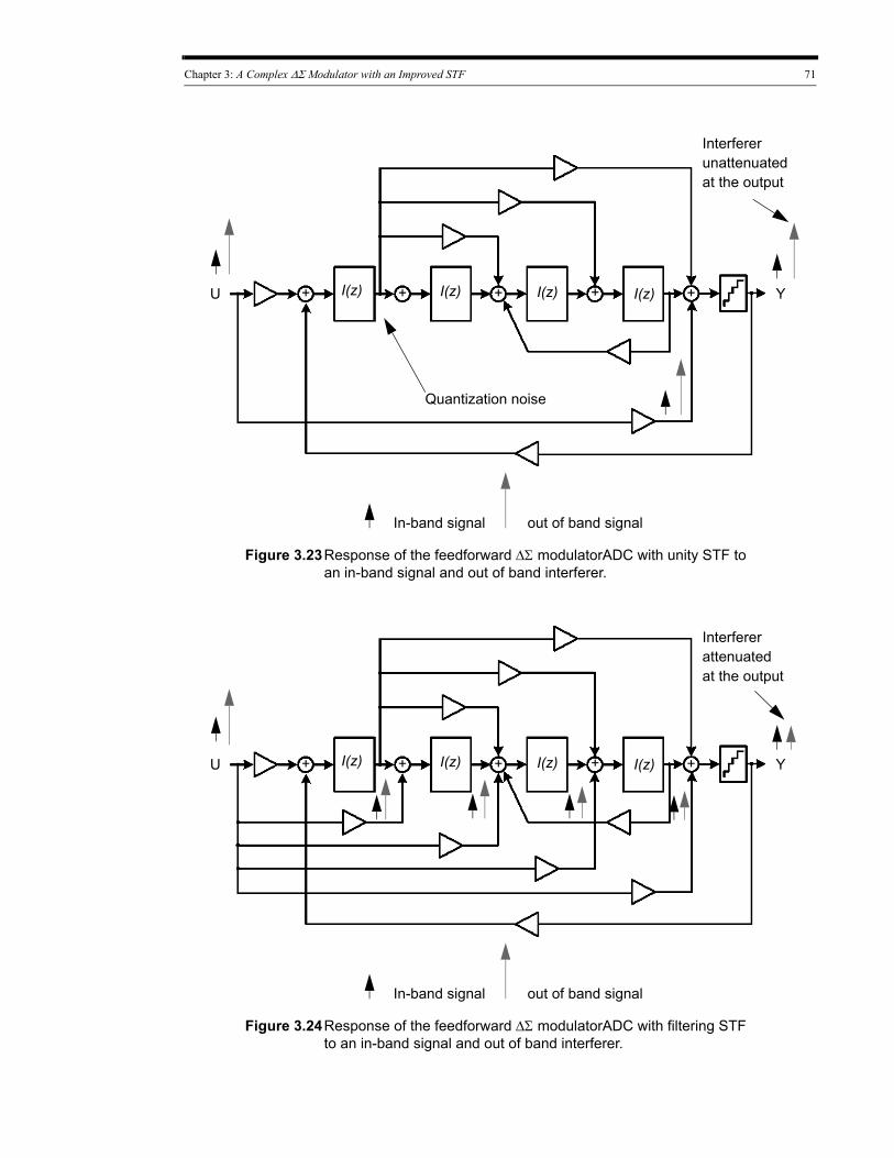
Chapter 3: A Complex ΔΣ Modulator with an Improved STF 71
U Y
out of band signal
Figure 3.23Response of the feedforward ΔΣ modulatorADC with unity STF to an in-band signal and out of band interferer.
I(z)I(z)I(z)I(z)
Quantization noise
++++ +
In-band signal
Interferer unattenuated at the output
U Y
out of band signal
Figure 3.24Response of the feedforward ΔΣ modulatorADC with filtering STF to an in-band signal and out of band interferer.
I(z)I(z)I(z)I(z) ++++ +
In-band signal
Interferer attenuated at the output
Chapter 3: A Complex ΔΣ Modulator with an Improved STF 72
The two ADCs were compared for the impact of opamp dc gain variation and coeffi-
cient mismatch on SNDR performance. For an opamp dc gain variation from 80 dB to 40
dB both the architectures show an SNDR degradation of less than 0.5 dB. Similarly, for a
coefficient mismatch of ±0.5% the two ADCs show an SNDR degradation less than 1 dB.
3.5.4 Stability Comparison
The proposed filtering ΔΣ modulator with optimized NTF poles was investigated for
stability. Two types of modulators were designed with a peak NTF gain of 12 dB. One
modulator was built with NTF poles arranged in butterworth order, and the second modu-
lator was designed with NTF poles optimized by the STF-NTF co-design algorithm. The
ΔΣ modulator with optimized NTF poles behaves well for inputs up to full-scale and
reaches a peak SNR of 88 dB. The modulator with NTF poles arranged in butterworth
order does not show any stability advantage over the modulator with optimized NTF
poles.
3.6 The STF-NTF Co-Design Optimization Algorithm for the Design of Complex ΔΣ Modulators
It is possible to derive complex transfer functions from the real prototypes by perform-
ing a simple frequency translation of the filter. The real prototype filter symmetric about
the dc is transformed into a non-zero IF complex filter symmetric about the IF. However, a
disadvantage of complex filters derived this way is that they are arithmetically symmetric.
Sometimes, it maybe desirable, for example, SSB modulation or demodulation, to derive
complex filters with asymmetric specifications. With the background knowledge devel-
oped in section 3.3, the optimization algorithm for an STF-NTF co-design for a complex
ΔΣ modulator can now be described as [5]:
• The zeros of the STF are derived using the pole-placement algorithm described in [1];
Chapter 3: A Complex ΔΣ Modulator with an Improved STF 73
• The Optimization algorithm proceeds with the minimization of the objective function,
given by:
NTF ω( ) 2 ωd
ωIFωs
2OSR---------------–
ωIFωs
2OSR---------------+
∫ (3.32)
• The constraints for the minimization of the objective function are
(e) the L 1 norm of the impulse response of the NTF NTF(z).
(f) the maximum radius for the NTF poles.
(g) the maximum-deviation of the STF over the passband
A fourth-order complex delta-sigma modulator was designed for the DTV receiver
specifications for the DVB and ATSC [11][12]. To avoid issues such as dc-offset that are
related to Zero-IF, the IF has been set at BW/2 (where BW corresponds to the signal band-
width for the particular standard). For example, for ATSC and DVB DTV standards with
signal bandwidths of 6 MHz and 8 MHz respectively, the IF has been set at a value of 3
MHz and 4 MHz respectively. For a maximum signal bandwidth of 8MHz, the sampling
frequency has been set at a value of 128 MHz, which corresponds to an over-sampling
ratio of 16.
In the first version of the modulator, the NTF zeros were distributed over the signal
bandwidth. In a second version, three of the NTF zeros were distributed over the signal
bandwidth and the fourth zero has been placed at the image frequency in order to reduce
the aliasing of image-band noise into the in-band region of the modulator [13]. Sacrificing
one of the NTF zeros degrades the signal-band quantization noise shaping of the modula-
tor, but it results in a modulator with higher immunity to coefficient mismatches. The
topic is further discussed in Chapter 4. For the DTV receiver application, it is advanta-
geous to design an asymmetric complex STF with greater attenuation in the image band.
An advantage of complex transfer functions not designed by a simple frequency shift of

Chapter 3: A Complex ΔΣ Modulator with an Improved STF 74
the real lowpass prototype filters lies in the fact that they can be designed to meet these
asymmetric requirements optimally.
Chapter 3: A Complex ΔΣ Modulator with an Improved STF 75
Figure 3.25Design of the STF-NTF using the optimization algorithm for : (a) NTF magnitude gain, (b) STF magnitude gain, (c)
NTF pole-zero plot, (d) STF pole-zero plot, (e) PSD plot of a complex ΔΣ modulator with STF and NTF transfer-functions as shown in (a) and (b)
L 1 3.5=
(a)
-64 64-32 0 32
20
0
-20
-40
-60
-80
Mag
nitu
de (d
B)
Frequency (MHz)16 48-16-48 -64 64-32 0 32
Frequency (MHz)16 48-16-48
0
-20
-40
-60
-80
Mag
nitu
de (d
B)
1-1
-1
1
(b)
(c) (d)
(e)0
0
Im(z)
Re(z)
1-1
-1
1
0
0
Im(z)
Re(z)
-64 64-32 0 32Frequency (MHz)
16 48-16-48-160-140-120-100
-80-60-40-20
0
Chapter 3: A Complex ΔΣ Modulator with an Improved STF 76
The algorithm starts with an initial STF zero placement derived using [1] and then pro-
ceeds with the minimization of the objective function (refer to equation (3.32)). Through
application of an iterative procedure involving fixed and moveable zeros of the transfer
function, which is a feature allowed by the complex filter approximation routines, it is
possible to experiment with different stop-band attenuations and the STF-NTF design.
Figure 3.25 shows the NTF and the STF, which have been designed using the optimization
algorithm for L 1 3.5= . With help of Mathematica, the transfer-functions were mapped
to the modulator coefficients shown in Figure 3.2. Figure 3.25(b) shows the asymmetric
filtering STF. The STF achieves a stop-band rejection of greater than 40 dB and 60 dB for
the positive and negative frequencies respectively. Figure 3.25(e) shows a 64k-bin output
spectrum of the modulator simulated in Matlab. With a 15-level DAC and at a sampling
frequency of 128 MHz, the complex ΔΣ modulator achieves an SNDR of 55 dB for a –3
dBFS tone input frequency of 4 MHz.
Figure 3.26 also shows the NTF and the STF designed using the optimization algorithm
for different values of the L 1 norm. Some of the things that can be observed from the fig-
ure are:
• Increasing the L 1 norm causes the NTF gain and the NTF attenuation to increase.
• Increasing the L 1 norm degrades the stop-band attenuation of the STF.
After mapping the transfer-functions to the modulator coefficients, a set of simulations
were performed in order to observe the SNDR of the modulator. Table 3.4 summarizes the
modulator performances for different signal and noise transfer functions generated using
the optimization algorithm. The transfer functions derived for the norm value of
L 1 6.5= 1 have been selected for the implementation of the proposed ΔΣ modulator.
1. By using the modulator stability condition derived in equation (3.22), the case
L 1 6.5= corresponds to an input signal more than 65% of the quantizer range, whereas
the case L 1 7.5= corresponds to an input signal less than 60% of the quantizer range.
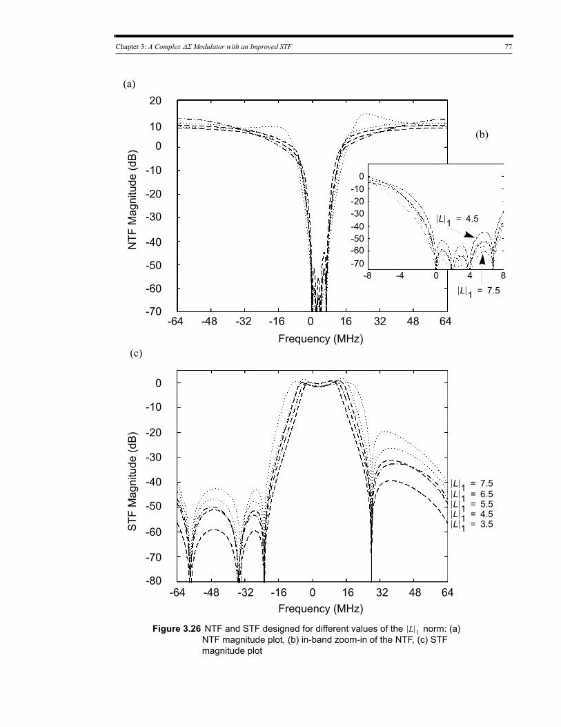
Chapter 3: A Complex ΔΣ Modulator with an Improved STF 77
Figure 3.26 NTF and STF designed for different values of the norm: (a) NTF magnitude plot, (b) in-band zoom-in of the NTF, (c) STF magnitude plot
L 1
-10
-20
-30
-40
-70
-60
NTF
Mag
nitu
de (d
B)
Frequency (MHz)
-50
10
20
0
-20
-30
-40
-50
-80
-70
STF
Mag
nitu
de (d
B)
Frequency (MHz)
-60
0
0
-64 -48 -32 -16 16 32 48 64
-10
-8 -4 0 4 8-70
-50
-30
-10
-60
-40
-20
0
(a)
(b)
(c)
L 1 3.5=
0-64 -48 -32 -16 16 32 48 64
L 1 4.5=L 1 5.5=L 1 6.5=L 1 7.5=
L 1 7.5=
L 1 4.5=
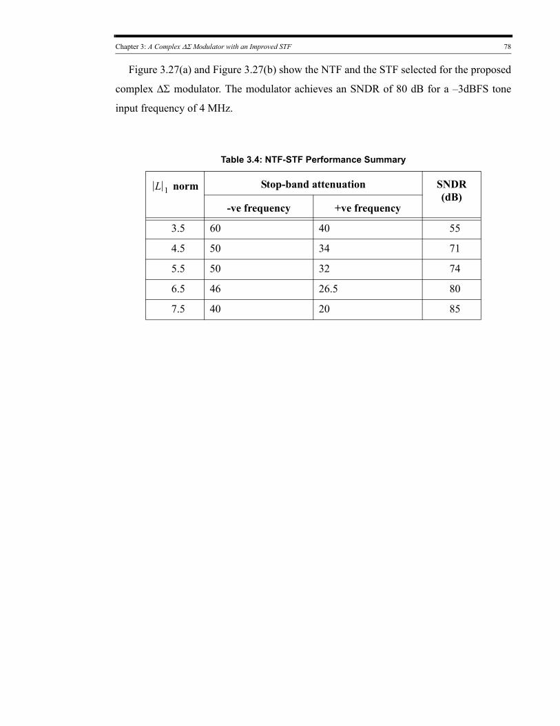
Chapter 3: A Complex ΔΣ Modulator with an Improved STF 78
Figure 3.27(a) and Figure 3.27(b) show the NTF and the STF selected for the proposed
complex ΔΣ modulator. The modulator achieves an SNDR of 80 dB for a –3dBFS tone
input frequency of 4 MHz.
Table 3.4: NTF-STF Performance Summary
L 1 norm Stop-band attenuation SNDR (dB)
-ve frequency +ve frequency
3.5 60 40 55
4.5 50 34 71
5.5 50 32 74
6.5 46 26.5 80
7.5 40 20 85
Chapter 3: A Complex ΔΣ Modulator with an Improved STF 79
Figure 3.27 Design of the STF-NTF using the optimization algorithm for |: (a) NTF magnitude gain, (b) STF magnitude gain,
(c) NTF pole-zero plot, (d) STF pole-zero plot, (e) PSD plot of a complex ΔΣ modulator with STF and NTF transfer-functions as shown in (a) and (b)
L 1 6.5=
(a)
-64 64-32 0 32
20
0
-20
-40
-60
-80
Mag
nitu
de (d
B)
Frequency (MHz)16 48-16-48 -64 64-32 0 32
Frequency (MHz)16 48-16-48
0
-20
-40
-60
-80
Mag
nitu
de (d
B)
1-1
-1
1
(b)
(c) (d)
(e)0
0
Im(z)
Re(z)
1-1
-1
1
0
0
Im(z)
Re(z)
-64 64-32 0 32Frequency (MHz)
16 48-16-48-160-140-120-100
-80-60-40-20
0
dB
Chapter 3: A Complex ΔΣ Modulator with an Improved STF 80
A set of fourth-order real NTFs was designed to meet a list of SQNR specifications of
101 dB, 94 dB, and 89 db. The real NTFs were designed for a signal bandwidth of π 16⁄
radians and an OSR of 16 (In terms of frequency this could correspond to a signal band-
width of 4 MHz and sampling frequency of 128 MHz). The zeros of the NTF were distrib-
uted over the signal band, and the poles are placed in the butterworth configuration. It is
possible to constrain the NTF pole position by specifying the out-of-band NTF gain. The
lowpass transfer functions were frequency shifted to an angular frequency of π 16⁄ (4
MHz) to realize complex transfer functions. The frequency shift was implemented by mul-
tiplying all NTF poles and zeros by ej π 16⁄( ) . As a result of the frequency shift the poles
and zeros of the NTF have no complex-conjugates and the magnitude response is not sym-
metric about dc. The STF shares poles with the NTF. To realize a complex filtering STF
zeros were inserted in the stop band region of the transfer function. To evaluate the effi-
cacy of the optimization algorithm, a set of complex NTFs and STFs were designed for the
same specifications using the algorithm proposed in section 3.6. Figure 3.28, Figure 3.29,
and Figure 3.30 show the NTFs and the STFs generated using these two different
approaches. A comparison of the two sets of STFs generated reveals that for the same
value of SQNR, the optimization algorithm generates STFs with flatter passband, and an
out-of-band rejection response which is at least superior by 7 dB (refer to Table 3.5).
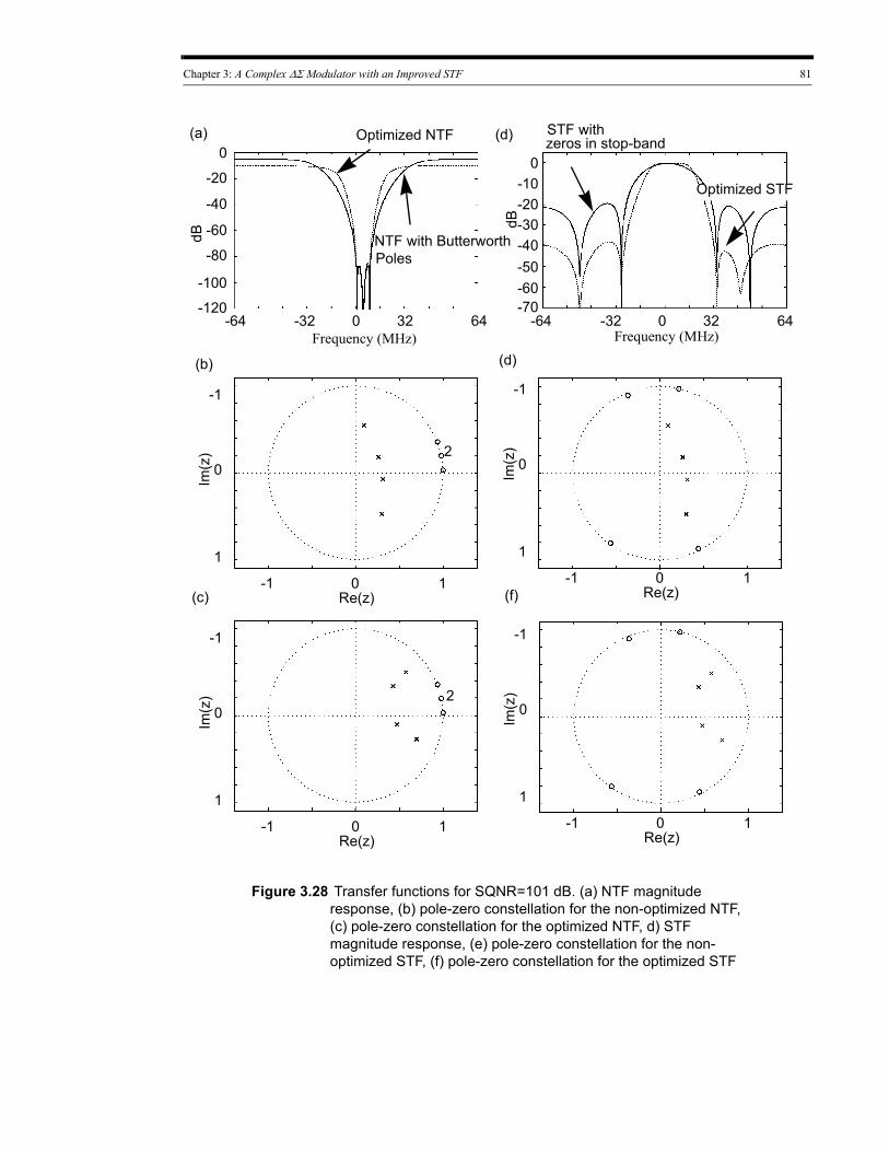
Chapter 3: A Complex ΔΣ Modulator with an Improved STF 81
Figure 3.28 Transfer functions for SQNR=101 dB. (a) NTF magnitude response, (b) pole-zero constellation for the non-optimized NTF, (c) pole-zero constellation for the optimized NTF, d) STF magnitude response, (e) pole-zero constellation for the non-optimized STF, (f) pole-zero constellation for the optimized STF
(a)
(b)
(c)
(d)
(d)
(f)
Optimized NTF
NTF with Butterworth Poles
STF with zeros in stop-band
64-32 0 32-120
-100
-80
-60
-40
-20
0
-64 64-32 0 32
-60-50-40-30-20-10
0
-64Frequency (MHz) Frequency (MHz)
dB
dB
2
2
1-1 0
1
-1
0
Re(z)
Im(z
)
1-1 0
1
-1
0
Re(z)
Im(z
)
1-1 0
1
-1
0
Re(z)
Im(z
)
1-1 0
1
-1
0
Re(z)
Im(z
)
-70
Optimized STF
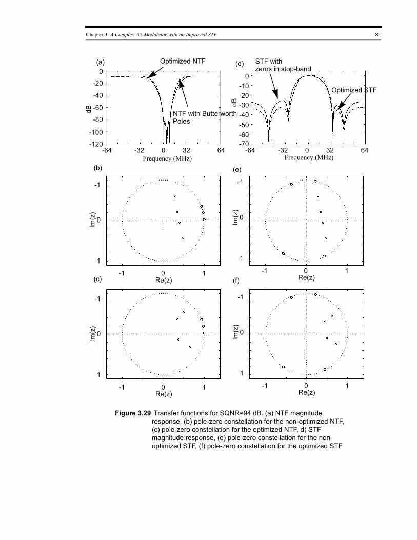
Chapter 3: A Complex ΔΣ Modulator with an Improved STF 82
Figure 3.29 Transfer functions for SQNR=94 dB. (a) NTF magnitude response, (b) pole-zero constellation for the non-optimized NTF, (c) pole-zero constellation for the optimized NTF, d) STF magnitude response, (e) pole-zero constellation for the non-optimized STF, (f) pole-zero constellation for the optimized STF
(a) Optimized NTF
NTF with Butterworth Poles
Optimized STF
64-32 0 32-120
-100
-80
-60
-40
-20
0
-64 64-32 0 32
-60-50-40-30-20-10
0
-64Frequency (MHz) Frequency (MHz)
dB
dB
1-1 0
1
-1
0
Re(z)
Im(z
)
1-1 0
1
-1
0
Re(z)
Im(z
)
1-1 0
1
-1
0
Re(z)
Im(z
)
1-1 0
1
-1
0
Re(z)
Im(z
)
-70
zeros in stop-bandSTF with
(b)
(c)
(d)
(e)
(f)
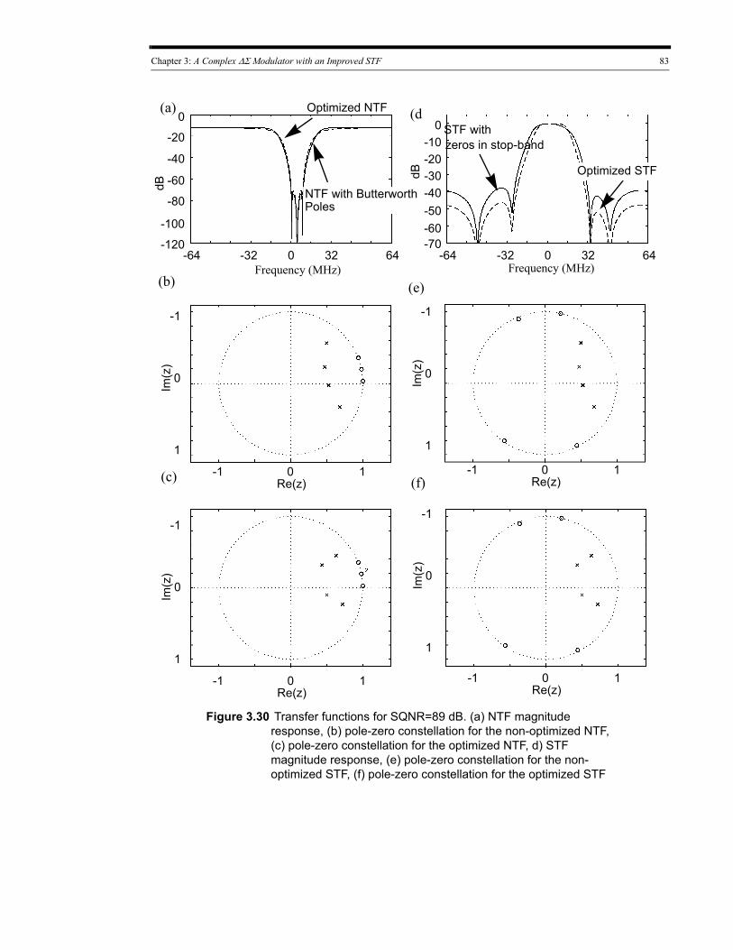
Chapter 3: A Complex ΔΣ Modulator with an Improved STF 83
Figure 3.30 Transfer functions for SQNR=89 dB. (a) NTF magnitude response, (b) pole-zero constellation for the non-optimized NTF, (c) pole-zero constellation for the optimized NTF, d) STF magnitude response, (e) pole-zero constellation for the non-optimized STF, (f) pole-zero constellation for the optimized STF
Optimized NTF
STF with zeros in stop-band
64-32 0 32-120
-100
-80
-60
-40
-20
0
-64 64-32 0 32
-60-50-40-30-20-10
0
-64Frequency (MHz) Frequency (MHz)
dB
dB
1-1 0
1
-1
0
Re(z)
Im(z
)
1-1 0
1
-1
0
Re(z)
Im(z
)
1-1 0
1
-1
0
Re(z)
Im(z
)
1-1 0
1
-1
0
Re(z)
Im(z
)
-70
Optimized STF
NTF with Butterworth Poles
(a)
(b)
(c)
(d
(e)
(f)
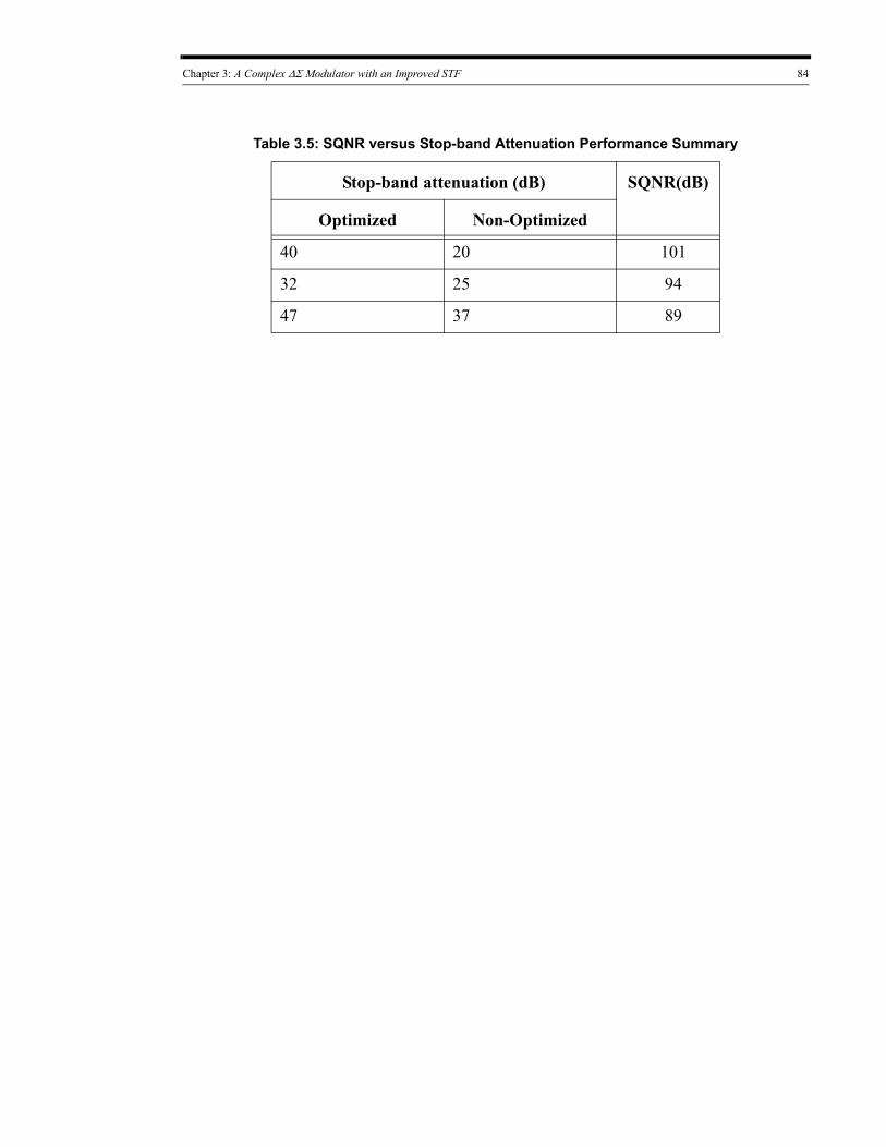
Chapter 3: A Complex ΔΣ Modulator with an Improved STF 84
Table 3.5: SQNR versus Stop-band Attenuation Performance Summary
Stop-band attenuation (dB) SQNR(dB)
Optimized Non-Optimized
40 20 101
32 25 94
47 37 89
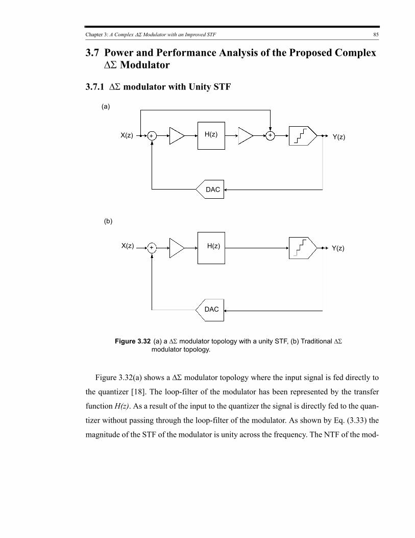
Chapter 3: A Complex ΔΣ Modulator with an Improved STF 85
3.7 Power and Performance Analysis of the Proposed Complex ΔΣ Modulator
3.7.1 ΔΣ modulator with Unity STF
X(z)
Figure 3.32 (a) a ΔΣ modulator topology with a unity STF, (b) Traditional ΔΣ modulator topology.
+
+
+ Y(z)
(a)
(b)
H(z)
H(z)
X(z) Y(z)
DAC
DAC
Figure 3.32(a) shows a ΔΣ modulator topology where the input signal is fed directly to
the quantizer [18]. The loop-filter of the modulator has been represented by the transfer
function H(z). As a result of the input to the quantizer the signal is directly fed to the quan-
tizer without passing through the loop-filter of the modulator. As shown by Eq. (3.33) the
magnitude of the STF of the modulator is unity across the frequency. The NTF of the mod-
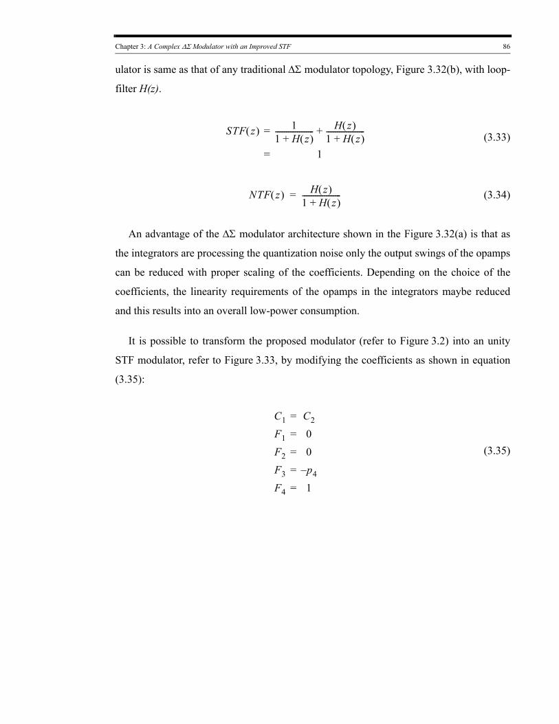
Chapter 3: A Complex ΔΣ Modulator with an Improved STF 86
ulator is same as that of any traditional ΔΣ modulator topology, Figure 3.32(b), with loop-
filter H(z).
STF z( ) = 11 H z( )+--------------------- H z( )
1 H z( )+---------------------+
= 1
NTF z( ) H z( )1 H z( )+---------------------=
(3.33)
(3.34)
An advantage of the ΔΣ modulator architecture shown in the Figure 3.32(a) is that as
the integrators are processing the quantization noise only the output swings of the opamps
can be reduced with proper scaling of the coefficients. Depending on the choice of the
coefficients, the linearity requirements of the opamps in the integrators maybe reduced
and this results into an overall low-power consumption.
It is possible to transform the proposed modulator (refer to Figure 3.2) into an unity
STF modulator, refer to Figure 3.33, by modifying the coefficients as shown in equation
(3.35):
C1 = C2
F1 = 0F2 = 0F3 = p4–F4 = 1
(3.35)
Chapter 3: A Complex ΔΣ Modulator with an Improved STF 87
B1
B2 + B3z-1
1z p1–--------------- z
z p2–---------------
C2
C2
X(z) 1z p3–--------------- z
z p4–---------------
Figure 3.33 Structure for a fourth-order ΔΣ modulator with a unity STF.
++++ Y(z)
1 p4z 1––( )
,
The proposed modulator with unity STF shown in the Figure 3.33 avoids signal sum-
mation at the input of the quantizer by moving the signal feedforward to the input of the
last integrator. A side-effect of signal feed-in at the last integrator input is that the integra-
tor is processing both the signal and the quantization noise. However, due to the noise-
shaping of the preceding stages of the modulator, the nonlinearities of the opamp in the
last stage of the modulator have little impact on the SNDR of the modulator.
Despite the advantage of low-per consumption, feedforward ΔΣ modulators have some
limitations that make them unsuitable for digitization of wireless signals. As discussed in
Chapter 2, feedforward ΔΣ modulators require a front-end filter to compensate for the out-
of-band peaking or slow roll off the STF [19]. The high-frequency interferers at the quan-
tizer input can also react with the quantizer noise, which is large at these frequencies, and
generate in-band intermodulation products, thus degrading the SNDR of the modulator
[20].
In the following sub-sections the proposed ΔΣ modulator (referred to as FADC in fur-
ther discussion), is compared to the feedforward ΔΣ modulator with unity STF. For rea-
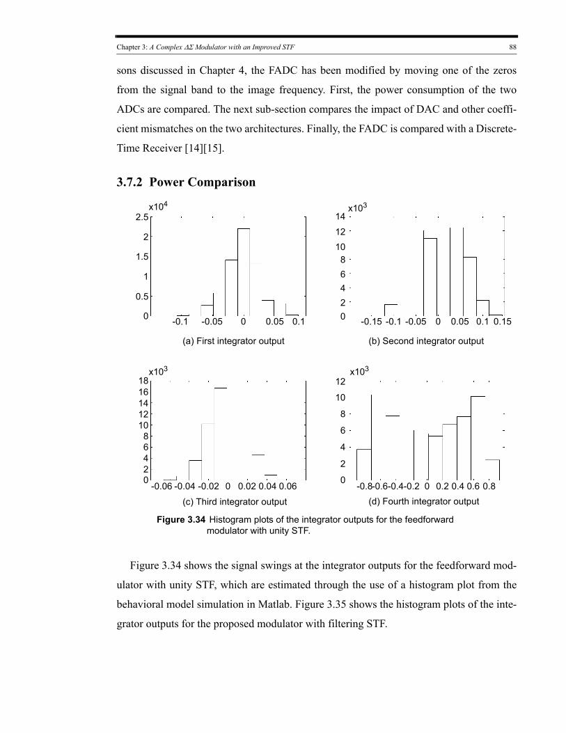
Chapter 3: A Complex ΔΣ Modulator with an Improved STF 88
sons discussed in Chapter 4, the FADC has been modified by moving one of the zeros
from the signal band to the image frequency. First, the power consumption of the two
ADCs are compared. The next sub-section compares the impact of DAC and other coeffi-
cient mismatches on the two architectures. Finally, the FADC is compared with a Discrete-
Time Receiver [14][15].
3.7.2 Power Comparison
Figure 3.34 Histogram plots of the integrator outputs for the feedforward modulator with unity STF.
-0.05 0.05
2.5
2
1.5
1
0.5
0 0.10-0.1 -0.1 0-0.05-0.15
14
1210
8
4
x104
6
02
0.05 0.1 0.15
x103
141210
8
46
02
x103
1618
-0.02 0.020-0.04-0.06 0.04 0.06
12
10
8
4
6
0
2
x103
-0.4 0-0.2-0.6 0.2 0.4 0.6 0.8-0.8
(a) First integrator output (b) Second integrator output
(c) Third integrator output (d) Fourth integrator output
Figure 3.34 shows the signal swings at the integrator outputs for the feedforward mod-
ulator with unity STF, which are estimated through the use of a histogram plot from the
behavioral model simulation in Matlab. Figure 3.35 shows the histogram plots of the inte-
grator outputs for the proposed modulator with filtering STF.
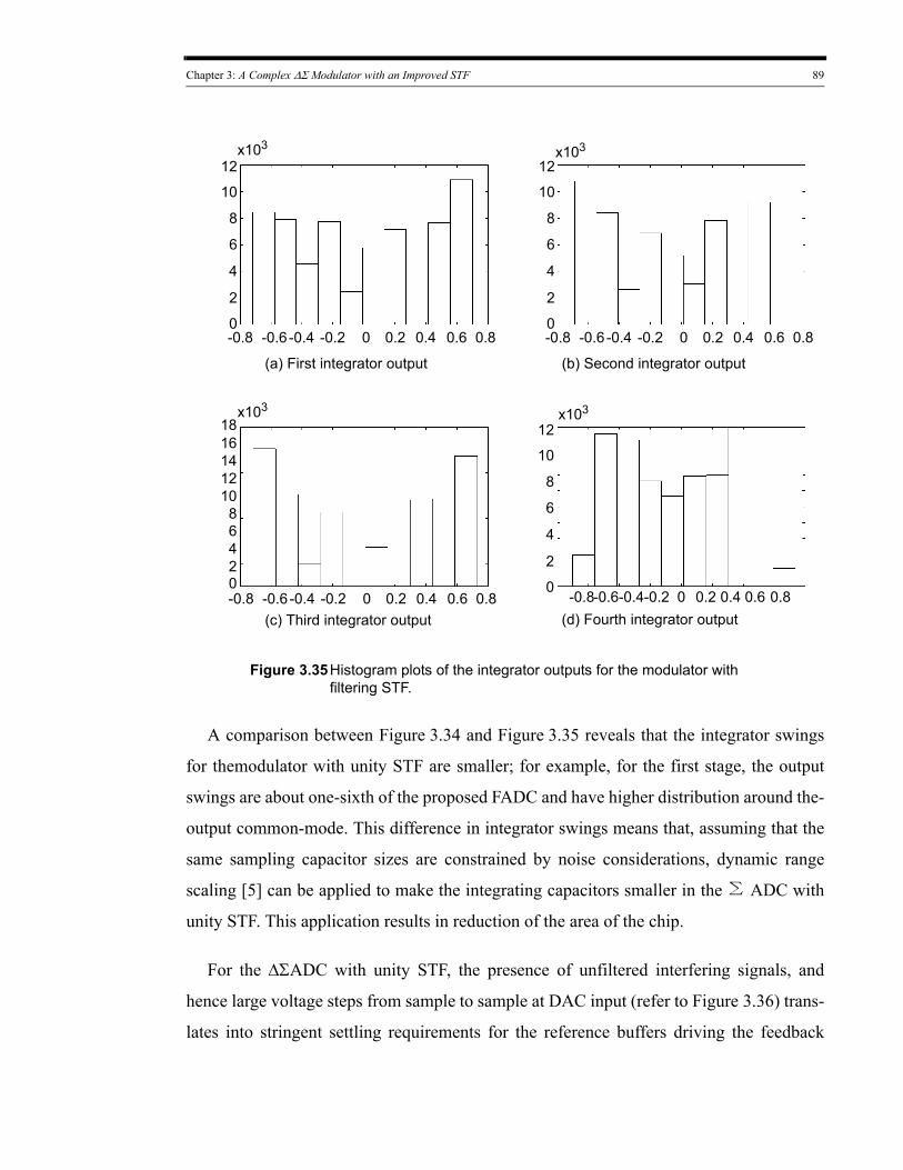
Chapter 3: A Complex ΔΣ Modulator with an Improved STF 89
-0.2 0.2 0.40-0.4
x103 x103
141210
8
46
02
x103
1618 12
10
8
4
6
0
2
x103
-0.4 0-0.2-0.6 0.2 0.4 0.6 0.8-0.8
12
10
8
4
6
0
2
0.6-0.6-0.8 0.8 -0.2 0.2 0.40-0.4
12
10
8
4
6
0
2
0.6-0.6-0.8 0.8
-0.2 0.2 0.40-0.4 0.6-0.6-0.8 0.8
Figure 3.35Histogram plots of the integrator outputs for the modulator with filtering STF.
(a) First integrator output (b) Second integrator output
(c) Third integrator output (d) Fourth integrator output
A comparison between Figure 3.34 and Figure 3.35 reveals that the integrator swings
for themodulator with unity STF are smaller; for example, for the first stage, the output
swings are about one-sixth of the proposed FADC and have higher distribution around the-
output common-mode. This difference in integrator swings means that, assuming that the
same sampling capacitor sizes are constrained by noise considerations, dynamic range
scaling [5] can be applied to make the integrating capacitors smaller in the Σ ADC with
unity STF. This application results in reduction of the area of the chip.
For the ΔΣADC with unity STF, the presence of unfiltered interfering signals, and
hence large voltage steps from sample to sample at DAC input (refer to Figure 3.36) trans-
lates into stringent settling requirements for the reference buffers driving the feedback
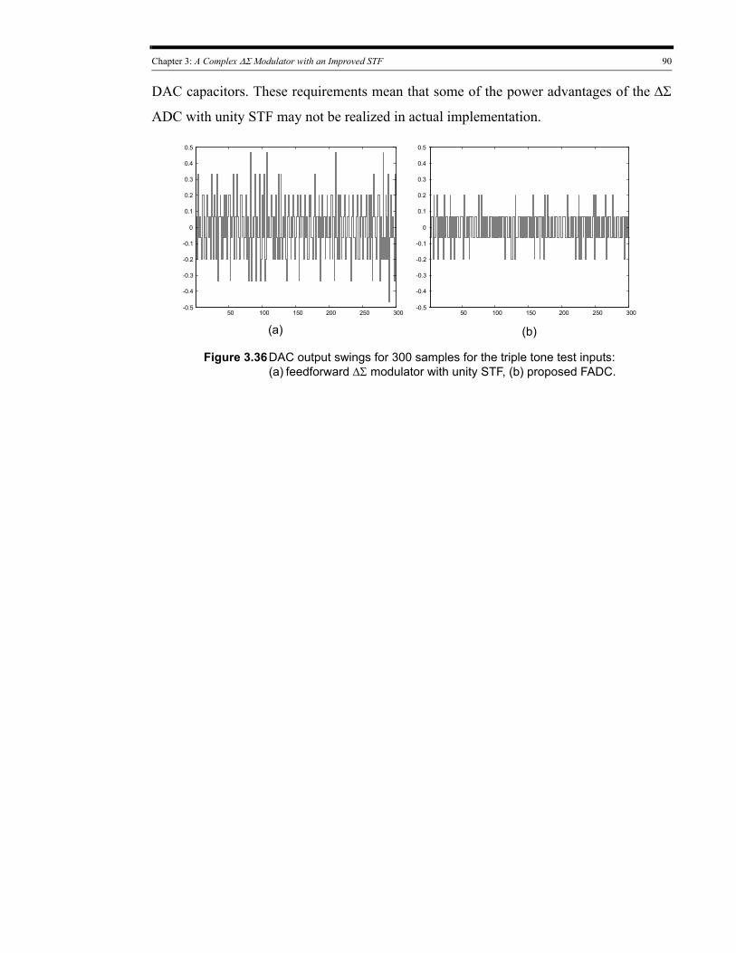
Chapter 3: A Complex ΔΣ Modulator with an Improved STF 90
DAC capacitors. These requirements mean that some of the power advantages of the ΔΣ
ADC with unity STF may not be realized in actual implementation.
Figure 3.36DAC output swings for 300 samples for the triple tone test inputs: (a) feedforward ΔΣ modulator with unity STF, (b) proposed FADC.
50 100 150 200 250 300-0.5
-0.4
-0.3
-0.2
-0.1
0
0.1
0.2
0.3
0.4
0.5
50 100 150 200 250 300-0.5
-0.4
-0.3
-0.2
-0.1
0
0.1
0.2
0.3
0.4
0.5
(a) (b)
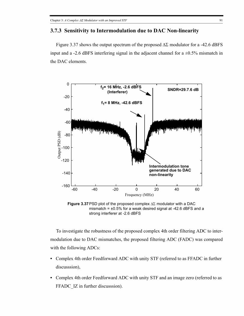
Chapter 3: A Complex ΔΣ Modulator with an Improved STF 91
3.7.3 Sensitivity to Intermodulation due to DAC Non-linearity
Figure 3.37 shows the output spectrum of the proposed ΔΣ modulator for a -42.6 dBFS
input and a -2.6 dBFS interfering signal in the adjacent channel for a ±0.5% mismatch in
the DAC elements.
Figure 3.37PSD plot of the proposed complex ΔΣ modulator with a DAC mismatch = ±0.5% for a weak desired signal at -42.6 dBFS and a strong interferer at -2.6 dBFS
SNDR=29.7.6 dB
-60 60-20 40Frequency (MHz)
200-40
-120
-100
-80
-60
-40
-20
0
-160
-140
Out
put P
SD (d
B)
f1= 8 MHz, -42.6 dBFS
f2= 16 MHz, -2.6 dBFS(Interferer)
Intermodulation tonegenerated due to DACnon-linearity
To investigate the robustness of the proposed complex 4th order filtering ADC to inter-
modulation due to DAC mismatches, the proposed filtering ADC (FADC) was compared
with the following ADCs:
• Complex 4th order Feedforward ADC with unity STF (referred to as FFADC in further
discusssion),
• Complex 4th order Feedforward ADC with unity STF and an image zero (referred to as
FFADC_IZ in further discusssion).
Chapter 3: A Complex ΔΣ Modulator with an Improved STF 92
The ADCs were simulated in SIMULINK (Matlab) under the following conditions:
(1) The discrete integrators have been modeled as shown in Figure 3.15 [17]. The inte-
grator model accounts for the finite dc gain and the output stauration voltages of the
opamps.
(2) The output saturation voltages of the integrators have been set at ±1.
(3) Dynamic range scaling was performed to make the swings at the integrator outputs
for the FFADC, FFADC_IZ, and FADC comparable.
(4) A mismatch of ±0.5% was assumed for the DAC elements.
The input to the modulators is a triple-tone consisting of: i) –46 dBFS input at 8 MHz,
ii) two interfereres of strength –6 dBFS each at the frequencies of 20 MHz and 36 MHz
respectively. This test pattern corresponds to the selectivity tests recommended for DVB-
T compliant receivers [12]. For this test input the FFADC and FFADC_IZ show an SNDR
of 43.5 dB and 32.3 dB respectively. The FADC achieves an SNDR of 32.5 dB for this test
input. Figure 3.38 shows the swings at the integrator outputs for the FADC. As is evident
from the figure, the integrators of the filtering ADC do not saturate for strong out-of-band
interfering signals.
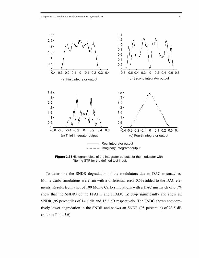
Chapter 3: A Complex ΔΣ Modulator with an Improved STF 93
-0.1 0.1 0.20-0.2
3.53
2.52
11.5
00.5
32.5
2
11.5
00.5
-0.2 0-0.1-0.3 0.1 0.2 0.3 0.4-0.4
3
2.5
2
1
1.5
0
0.5
0.3-0.3-0.4 0.4 -0.2 0.2 0.40-0.4
1.21.00.8
0.40.6
00.2
0.6-0.6-0.8 0.8
-0.2 0.2 0.40-0.4 0.6-0.6-0.8
Figure 3.38Histogram plots of the integrator outputs for the modulator with filtering STF for the defined test input.
(a) First integrator output (b) Second integrator output
(c) Third integrator output (d) Fourth integrator output
1.4
3.5
Real Integrator outputImaginary Integrator output
To determine the SNDR degradation of the modulators due to DAC mismatches,
Monte Carlo simulations were run with a differential error 0.5% added to the DAC ele-
ments. Results from a set of 100 Monte Carlo simulations with a DAC mismatch of 0.5%
show that the SNDRs of the FFADC and FFADC_IZ drop significantly and show an
SNDR (95 percentile) of 14.6 dB and 15.2 dB respectively. The FADC shows compara-
tively lower degradation in the SNDR and shows an SNDR (95 percentile) of 23.5 dB
(refer to Table 3.6)
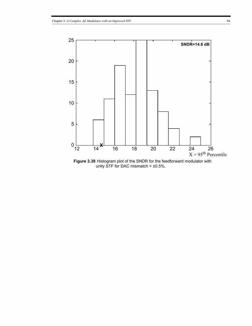
Chapter 3: A Complex ΔΣ Modulator with an Improved STF 94
Figure 3.39 Histogram plot of the SNDR for the feedforward modulator with unity STF for DAC mismatch = ±0.5%.
12 14 16 18 20 22 24 260
5
10
15
20
25
X
SNDR=14.6 dB
X = 95th Percentile
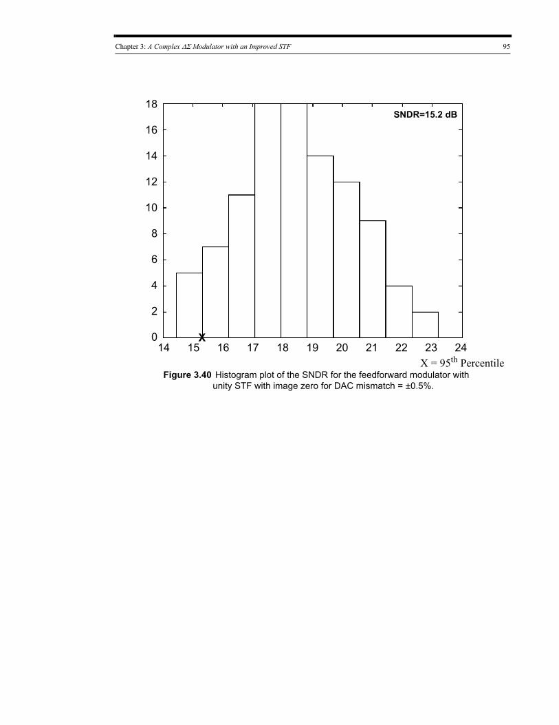
Chapter 3: A Complex ΔΣ Modulator with an Improved STF 95
Figure 3.40 Histogram plot of the SNDR for the feedforward modulator with unity STF with image zero for DAC mismatch = ±0.5%.
14 16 17 18 19 20 21 220
2
6
10
14
18
X
16
12
8
4
15 23 24
SNDR=15.2 dB
X = 95th Percentile
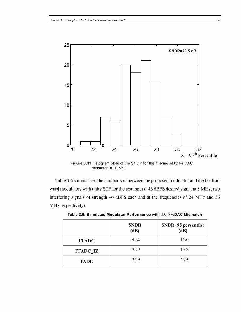
Chapter 3: A Complex ΔΣ Modulator with an Improved STF 96
Figure 3.41Histogram plots of the SNDR for the filtering ADC for DAC mismatch = ±0.5%.
20 22 24 26 28 30 320
5
10
15
20
25
X
SNDR=23.5 dB
X = 95th Percentile
Table 3.6 summarizes the comparison between the proposed modulator and the feedfor-
ward modulators with unity STF for the test input (–46 dBFS desired signal at 8 MHz, two
interfering signals of strength –6 dBFS each and at the frequencies of 24 MHz and 36
MHz respectively).
Table 3.6: Simulated Modulator Performance with 0.5± %DAC Mismatch
SNDR(dB)
SNDR (95 percentile)(dB)
FFADC 43.5 14.6
FFADC_IZ 32.3 15.2
FADC 32.5 23.5
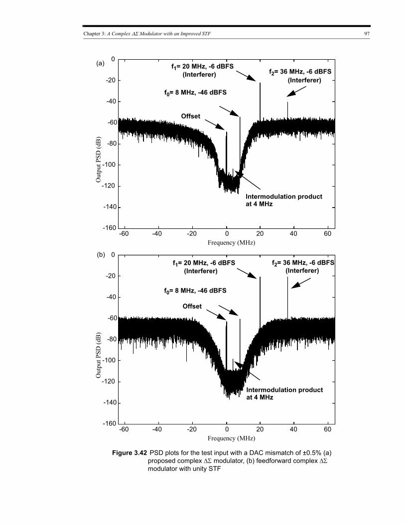
Chapter 3: A Complex ΔΣ Modulator with an Improved STF 97
-60 60-20 40Frequency (MHz)
200-40
-120
-100
-80
-60
-40
-20
0
-160
-140
Out
put P
SD (d
B)
-60 60-20 40Frequency (MHz)
200-40
-120
-100
-80
-60
-40
-20
0
-160
-140
Out
put P
SD (d
B)
Figure 3.42 PSD plots for the test input with a DAC mismatch of ±0.5% (a) proposed complex ΔΣ modulator, (b) feedforward complex ΔΣ modulator with unity STF
(a)
(b)
f0= 8 MHz, -46 dBFS
f1= 20 MHz, -6 dBFS(Interferer) f2= 36 MHz, -6 dBFS
(Interferer)
f0= 8 MHz, -46 dBFS
f1= 20 MHz, -6 dBFS(Interferer)
f2= 36 MHz, -6 dBFS(Interferer)
Intermodulation productat 4 MHz
Intermodulation productat 4 MHz
Offset
Offset
Chapter 3: A Complex ΔΣ Modulator with an Improved STF 98
For a reduced DAC mismatch of ±0.1% the SNDR (95th percentile) of the FADC
degrades to 31.63 dB. For the FFADC and FFADC_IZ the SNDR degrades to 27.3 dB and
28.5 dB respectively.
3.7.4 Comparison with a Discrete-Time Receiver [14][15]
A DTV receiver includes an IF filter and a demodulator for demodulation and error-
correction of the IF signals. Currently, analog TV broadcasting and digital TV broadcast-
ing are coexisting; hence, these interferences are mainly undesired digital TV and/or ana-
log TV channels. The power levels of those adjacent interfering channels can be higher
than the desired channel, for example, 40 dB for ATSC signals [11]. In addition to the lin-
earity requirement, it is necessary that the IF filters attenuate the interfering channels
enough so that the ADC in the demodulator is not saturated. For example, for ATSC the IF
filter has to provide over 50 dB attenuation for the adjacent channel.
The possible ways to implement IF filtering in a DTV receiver are:
Option 1- The IF filter is typically implemented using SAW filters and the receiver uses
a bank of SAW filters to accomodate multi-standards. An advanatge of the SAW filters is
the attenuation of the adjacent channels which results into a reduce dynamic range
requiremenst of the ADC. However, to achieve a higher level of integration and hence low
cost it is necessary to integrate the IF filters on the chip.
Option 2- Two possible filter technologies for integrating IF filters on chip are: the con-
tinuous-time filters and the switched-capacitor filter. Though, the continuous-time filters
consume less power, but they need calibration to set the frequency characteristics accu-
rately. Also, the requirement to support multi-standards adds to the tuning complexity for
these filters.
Unless, a narrow band IF filter is implemented for adjacent channel rejection, an ADC
with greater than 11 bit resolution is required to digitize the adjacent interfering channel
(refer to Table 3.7).
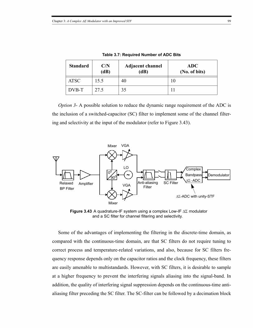
Chapter 3: A Complex ΔΣ Modulator with an Improved STF 99
Table 3.7: Required Number of ADC Bits
Standard C/N(dB)
Adjacent channel (dB)
ADC (No. of bits)
ATSC 15.5 40 10
DVB-T 27.5 35 11
Option 3- A possible solution to reduce the dynamic range requirement of the ADC is
the inclusion of a switched-capacitor (SC) filter to implement some of the channel filter-
ing and selectivity at the input of the modulator (refer to Figure 3.43).
LO
VGAMixer
Amplifier
00
Mixer
900
ComplexBandpassΔΣ−ADC
VGAAnti-aliasing
Filter
Demodulator
Relaxed BP Filter
SC Filter
ΔΣ-ADC with unity-STF
Figure 3.43 A quadrature-IF system using a complex Low-IF ΔΣ modulator and a SC filter for channel filtering and selectivity.
Some of the advantages of implementing the filtering in the discrete-time domain, as
compared with the continuous-time domain, are that SC filters do not require tuning to
correct process and temperature-related variations, and also, because for SC filters fre-
quency response depends only on the capacitor ratios and the clock frequency, these filters
are easily amenable to multistandards. However, with SC filters, it is desirable to sample
at a higher frequency to prevent the interfering signals aliasing into the signal-band. In
addition, the quality of interfering signal suppression depends on the continuous-time anti-
aliasing filter preceding the SC filter. The SC-filter can be followed by a decimation block
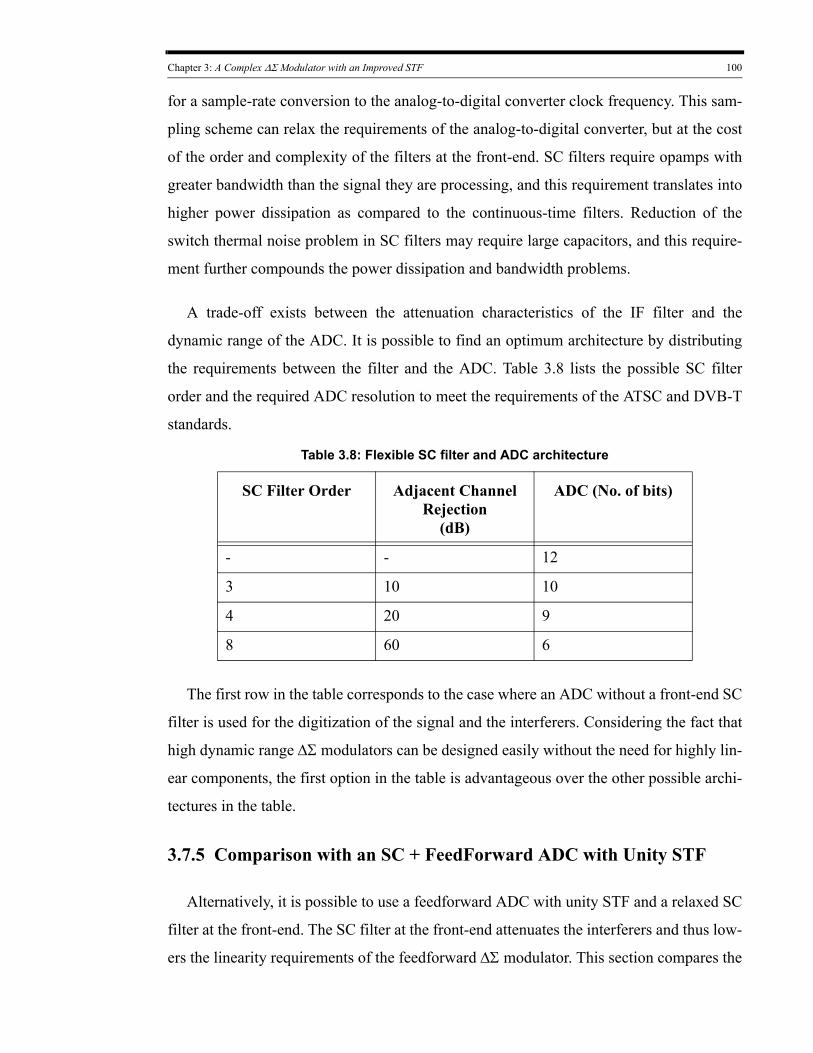
Chapter 3: A Complex ΔΣ Modulator with an Improved STF 100
for a sample-rate conversion to the analog-to-digital converter clock frequency. This sam-
pling scheme can relax the requirements of the analog-to-digital converter, but at the cost
of the order and complexity of the filters at the front-end. SC filters require opamps with
greater bandwidth than the signal they are processing, and this requirement translates into
higher power dissipation as compared to the continuous-time filters. Reduction of the
switch thermal noise problem in SC filters may require large capacitors, and this require-
ment further compounds the power dissipation and bandwidth problems.
A trade-off exists between the attenuation characteristics of the IF filter and the
dynamic range of the ADC. It is possible to find an optimum architecture by distributing
the requirements between the filter and the ADC. Table 3.8 lists the possible SC filter
order and the required ADC resolution to meet the requirements of the ATSC and DVB-T
standards.
Table 3.8: Flexible SC filter and ADC architecture
SC Filter Order Adjacent Channel Rejection
(dB)
ADC (No. of bits)
- - 12
3 10 10
4 20 9
8 60 6
The first row in the table corresponds to the case where an ADC without a front-end SC
filter is used for the digitization of the signal and the interferers. Considering the fact that
high dynamic range ΔΣ modulators can be designed easily without the need for highly lin-
ear components, the first option in the table is advantageous over the other possible archi-
tectures in the table.
3.7.5 Comparison with an SC + FeedForward ADC with Unity STF
Alternatively, it is possible to use a feedforward ADC with unity STF and a relaxed SC
filter at the front-end. The SC filter at the front-end attenuates the interferers and thus low-
ers the linearity requirements of the feedforward ΔΣ modulator. This section compares the
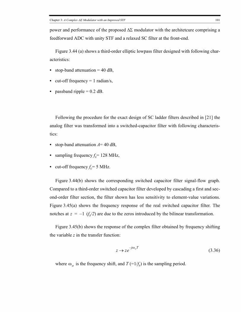
Chapter 3: A Complex ΔΣ Modulator with an Improved STF 101
power and performance of the proposed ΔΣ modulator with the architetcure comprising a
feedforward ADC with unity STF and a relaxed SC filter at the front-end.
Figure 3.44 (a) shows a third-order elliptic lowpass filter designed with following char-
acteristics:
• stop-band attenuation = 40 dB,
• cut-off frequency = 1 radian/s,
• passband ripple = 0.2 dB.
Following the procedure for the exact design of SC ladder filters described in [21] the
analog filter was transformed into a switched-capacitor filter with following characteris-
tics:
• stop-band attenuation A= 40 dB,
• sampling frequency fs= 128 MHz,
• cut-off frequency fc= 5 MHz.
Figure 3.44(b) shows the corresponding switched capacitor filter signal-flow graph.
Compared to a third-order switched capacitor filter developed by cascading a first and sec-
ond-order filter section, the filter shown has less sensitivity to element-value variations.
Figure 3.45(a) shows the frequency response of the real switched capacitor filter. The
notches at z 1–= (fs/2) are due to the zeros introduced by the bilinear transformation.
Figure 3.45(b) shows the response of the complex filter obtained by frequency shifting
the variable z in the transfer function:
z zej– ωoT
→ (3.36)
where ωo is the frequency shift, and T (=1/fs) is the sampling period.
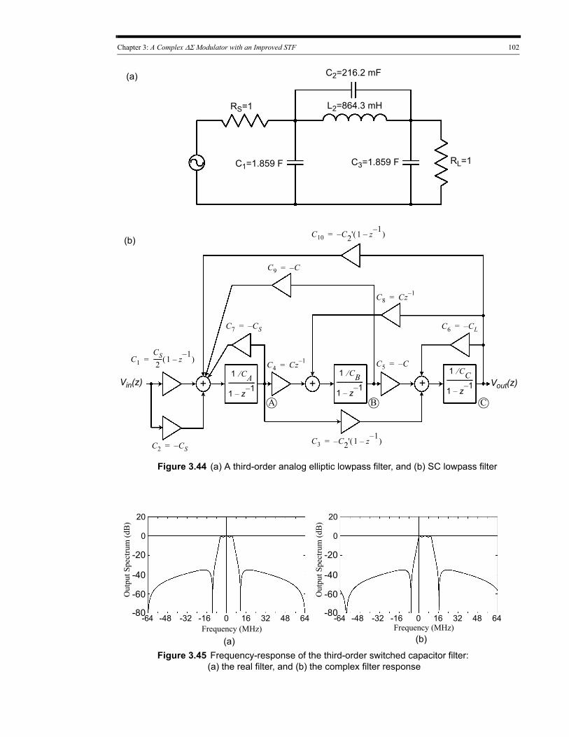
Chapter 3: A Complex ΔΣ Modulator with an Improved STF 102
1 CA⁄
1 z 1––------------------- +++Vin(z) Vout(z)
1 CB⁄
1 z 1––-------------------
1 CC⁄
1 z 1––-------------------
C7 CS–=
C3 C– 2' 1 z 1––( )=
C4 Cz 1–= C5 C–=C1CS2
------ 1 z 1––( )=
C2 CS–=
C6 C– L=
C8 Cz 1–=
C9 C–=
RL=1
RS=1
C1=1.859 F C3=1.859 F
C2=216.2 mF
L2=864.3 mH
Figure 3.44 (a) A third-order analog elliptic lowpass filter, and (b) SC lowpass filter
C10 C– 2' 1 z 1––( )=
CA B
(a)
(b)
Figure 3.45 Frequency-response of the third-order switched capacitor filter: (a) the real filter, and (b) the complex filter response
6432 4816-16-32-48-64 0
0
-20
-40
-60
-80
20
Out
put S
pect
rum
(dB
)
Frequency (MHz)6432 4816-16-32-48-64 0
0
-20
-40
-60
-80
20
Out
put S
pect
rum
(dB
)
Frequency (MHz)
(a) (b)
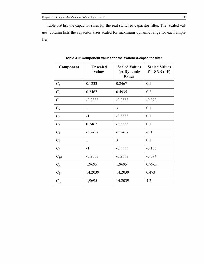
Chapter 3: A Complex ΔΣ Modulator with an Improved STF 103
Table 3.9 list the capacitor sizes for the real switched capacitor filter. The ‘scaled val-
ues’ column lists the capacitor sizes scaled for maximum dynamic range for each ampli-
fier.
Table 3.9: Component values for the switched-capacitor filter.
Component Unscaled values
Scaled Values for Dynamic
Range
Scaled Values for SNR (pF)
C1 0.1233 0.2467 0.1
C2 0.2467 0.4935 0.2
C3 -0.2338 -0.2338 -0.070
C4 1 3 0.1
C5 -1 -0.3333 0.1
C6 0.2467 -0.3333 0.1
C7 -0.2467 -0.2467 -0.1
C8 1 3 0.1
C9 -1 -0.3333 -0.135
C10 -0.2338 -0.2338 -0.094
CA 1.9695 1.9695 0.7965
CB 14.2039 14.2039 0.473
CC 1,9695 14.2039 4.2
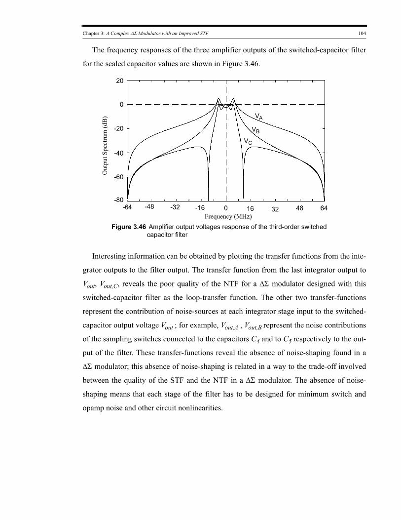
Chapter 3: A Complex ΔΣ Modulator with an Improved STF 104
The frequency responses of the three amplifier outputs of the switched-capacitor filter
for the scaled capacitor values are shown in Figure 3.46.
Figure 3.46 Amplifier output voltages response of the third-order switched capacitor filter
6432 4816-16-32-48-64 0
0
-20
-40
-60
-80
20
Out
put S
pect
rum
(dB
)
Frequency (MHz)
VA
VB
VC
Interesting information can be obtained by plotting the transfer functions from the inte-
grator outputs to the filter output. The transfer function from the last integrator output to
Vout, Vout,C, reveals the poor quality of the NTF for a ΔΣ modulator designed with this
switched-capacitor filter as the loop-transfer function. The other two transfer-functions
represent the contribution of noise-sources at each integrator stage input to the switched-
capacitor output voltage Vout ; for example, Vout,A , Vout,B represent the noise contributions
of the sampling switches connected to the capacitors C4 and to C5 respectively to the out-
put of the filter. These transfer-functions reveal the absence of noise-shaping found in a
ΔΣ modulator; this absence of noise-shaping is related in a way to the trade-off involved
between the quality of the STF and the NTF in a ΔΣ modulator. The absence of noise-
shaping means that each stage of the filter has to be designed for minimum switch and
opamp noise and other circuit nonlinearities.
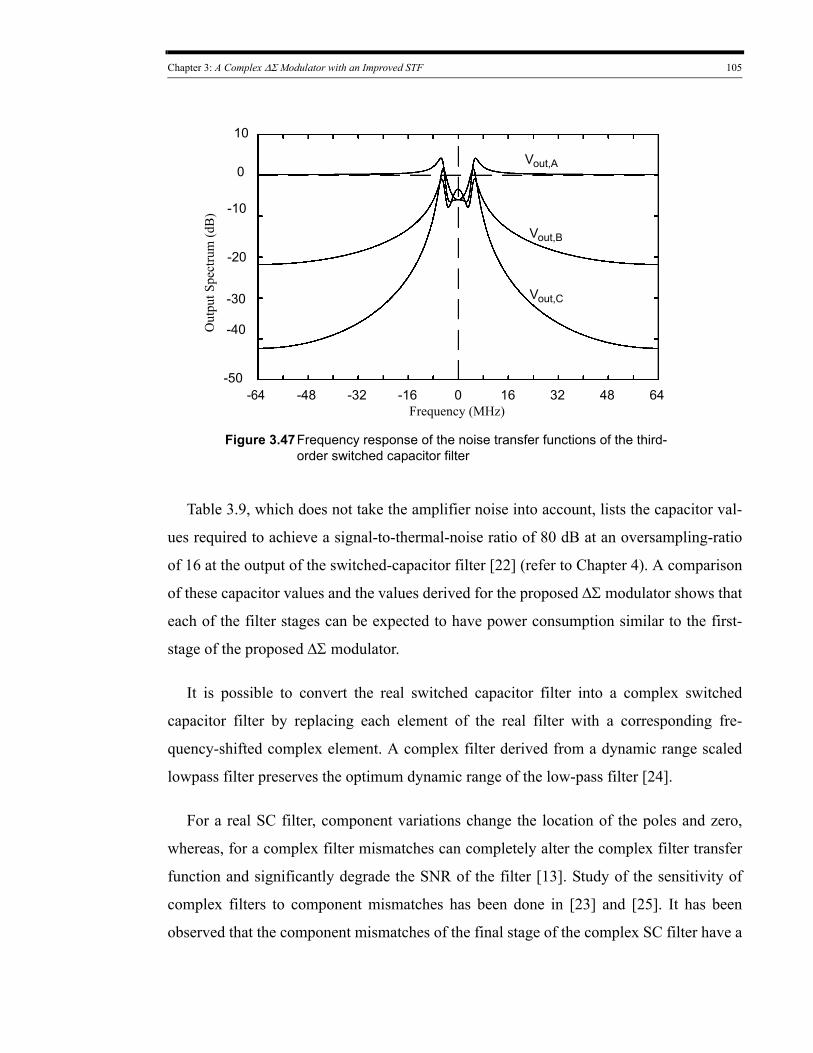
Chapter 3: A Complex ΔΣ Modulator with an Improved STF 105
Figure 3.47Frequency response of the noise transfer functions of the third-order switched capacitor filter
6432 4816-16-32-48-64 0
0
-10
-20
-30
-40
10
Out
put S
pect
rum
(dB
)
Frequency (MHz)
-50
Vout,A
Vout,B
Vout,C
Table 3.9, which does not take the amplifier noise into account, lists the capacitor val-
ues required to achieve a signal-to-thermal-noise ratio of 80 dB at an oversampling-ratio
of 16 at the output of the switched-capacitor filter [22] (refer to Chapter 4). A comparison
of these capacitor values and the values derived for the proposed ΔΣ modulator shows that
each of the filter stages can be expected to have power consumption similar to the first-
stage of the proposed ΔΣ modulator.
It is possible to convert the real switched capacitor filter into a complex switched
capacitor filter by replacing each element of the real filter with a corresponding fre-
quency-shifted complex element. A complex filter derived from a dynamic range scaled
lowpass filter preserves the optimum dynamic range of the low-pass filter [24].
For a real SC filter, component variations change the location of the poles and zero,
whereas, for a complex filter mismatches can completely alter the complex filter transfer
function and significantly degrade the SNR of the filter [13]. Study of the sensitivity of
complex filters to component mismatches has been done in [23] and [25]. It has been
observed that the component mismatches of the final stage of the complex SC filter have a
Chapter 3: A Complex ΔΣ Modulator with an Improved STF 106
greater effect on the stop-band response, and the final stage of the complex SC filter
should be designed with large and carefully matched devices. This is unlike a ΔΣ modula-
tor, in which the first integrator stage amplifier is typically dominant in the modulator
noise, linearity, and power requirements.
The conclusion is that, due to the reduced power and linearity requirements of the
amplifier, feedforward ΔΣ modulator with unity STF is an attractive option, however this
receiver architecture results into an increased complexity of the filter at the front-end. The
noise and matching requirements of these front-end filters outweigh the advantages gained
from the feeforward ΔΣ modulator architecture.
3.8 Advantages of the proposed ΔΣ Modulator architecture
The proposed ΔΣ modulator offers several advantages over the traditional ΔΣ modula-
tor architectures:
• Unlike the feedforward architecture, the proposed ΔΣ modulator avoids having a
weighted summation before the quantizer, and, hence, issues like signal attenuation and
reference scaling for the purpose of passive summation or power dissipation in the case
of active summation have been eliminated. In the proposed ΔΣ modulator, the summa-
tion of the signals has been distributed at various integrator inputs.
• Due to the low-pass nature of the STF, the modulator avoids stability issues related to
the peaking of the STF at higher signal frequencies. Compared to the traditional feed-
forward ΔΣ modulator, the proposed modulator shows significantly reduced sensitivity
to process variations and coefficient mismatches. This reduction occurs because of the
filtering nature of the STF.
• With a filtering STF and stop band attenuation greater than 30dB, the ΔΣ modulator
reduces intermodulation of the desired signal and the interfering signals at the input of
the quantizer, and also avoids feedback of the high-frequency interfering signals at the
input of the modulator.
Chapter 3: A Complex ΔΣ Modulator with an Improved STF 107
• Figure 3.48 shows digital signal processing in a typical ΔΣ modulator-based DTV
receiver. The task of the complex demodulator includes demodulation and recovery of
the transmitted bit sequence. Prior to lowering the bit-rate, the decimation filters at the
output of the complex bandpass ΔΣ ADC attenuate the high-frequency quantization
noise and out-of-band interferers components that may alias into the signal band during
decimation. The order of the decimating filters is decided by the required attenuation of
the quantization noise and the interfering signals at the input of the decimating filters.
The interfering signals are attenuated by the antialias filter at the input of the ADC. The
filtering STF of the ADC further relaxes the decimation filter design by attenuating
these interferers.
• The role of the digital quadrature mixer, the complex NCO in Figure 3.48, consists of
correcting any frequency offset errors that may occur between the carrier frequency and
the symbol rate and converting the complex signal from low-IF to zero-IF. The base-
band signal at the output of the mixer is subsequently low-pass filtered in order to atten-
uate image frequencies and other sum frequencies generated by the mixing operation.
The output of the low-pass filters goes to a data recovery block where the transmitted
data bit sequence is recovered. The low-pass filters act as image rejection filters, and
the order of these low-pass filters depends on the attenuation desired for the image fre-
quencies. An asymmetric filtering ADC with significant attenuation for image frequen-
cies reduces the complexity of these low-pass filters.
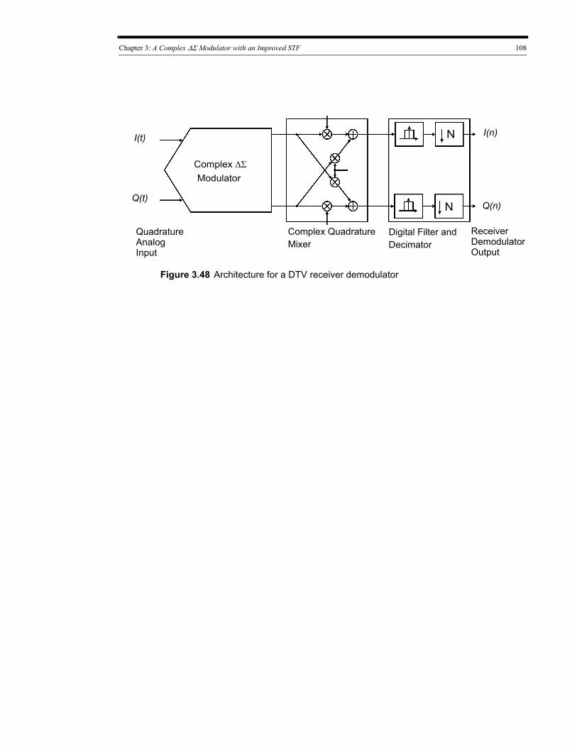
Chapter 3: A Complex ΔΣ Modulator with an Improved STF 108
Figure 3.48 Architecture for a DTV receiver demodulator
Complex ΔΣ Modulator
N
N
Complex Quadrature Digital Filter andDecimatorMixer
Receiver Demodulator Output
Quadrature AnalogInput
I(t)
Q(t)
I(n)
Q(n)
Chapter 3: A Complex ΔΣ Modulator with an Improved STF 109
References[1] K. Martin,‘‘Approximation of Complex IIR Bandpass Filters Without Arithmetic
Symmetry,” IEEE Trans. Circuits and Systems-I, vol. 52, No. 4, pp. 794-803, April 2005.
[2] S. R. Norsworthy, R. Schreier, and G. C. Temes, Eds., Delta-Sigma Data Converters: Theory, Design, and Simulation. New York: IEEE Press. ISBN 0780310454.
[3] Richard W. Daniels, Approximation Methods for Electronic Filter Design: With Applications to Passive, Active, and Digital Networks, McGraw-Hill, 1974.
[4] Peter O. Brackett, A.S.Sedra, Filter Theory and Design: Active and Passive, Matrix Series in Circuits and Systems.
[5] Bupesh Pandita, K. W. Martin, “Designing Complex Delta Sigma Modulators with Signal-Transfer Functions having Good Stop-Band Attenuation,” pp. 3626-3629, ISCAS 2007.
[6] Richard Schreier and Gabor C. Temes, Understanding Delta-Sigma Data Converters. Wiley-IEEE Press, 2004. ISBN 0-471-46585-2.
[7] KiYoung Nam, Sang-Min Lee, D. K. Su, and B. A. Wooley, “A low-voltage low-power sigma-delta modulator for broadband analog-to-digital conversion,” IEEE J. Solid-State Circuits, vol. 40, no. 9, pp. 1855 – 1864, Sep. 2005.
[8] Richard Schreier, “An Empirical Study of High-Order Single-Bit Delta-Sigma Modulators,” IEEE Transactions on circuits and systems-II: analog and digital signal processing, vol. 40, no. 8, August 1993.
[9] John. G. Kenney, and L. Richard Carley, “Design of multibit noiseshapingdata converters,” Analog Integrated Circuits and Signal Processing, vol. 3, no. 3, May 1993.
[10] The Math Works, Inc., Matlab, Version 6.4, Natick, Massachusets: The Math Works, Inc.,
[11] ATSC Recommended Practice: Receiver Performance Guidelines, ATSC A/74, June 2004, pp 13-14.
[12] Mobile and Portable DVB-T/H Radio Access Interface Specification, EICTA MBRAI-02.
[13] S.A. Jantzi, K. W. Martin, and A. S. Sedra, “The effects of mismatch in complex bandpass ΔΣ modulators,” IEEE International Symposium on Circuits and Systems, vol. 1, 12-15, May 1996, pp. 227-23.
[14] R. B. Staszewski, K. Muhammad, D. Leipold, Chih-Ming Hung, Yo-Chuol Ho, J. L. Wallberg, C. Fernando, K. Maggio, R. Staszewski, T. Jung, Jinseok Koh, S. John, Irene Yuanying Deng, V. Sarda, O. Moreira-Tamayo, V. Mayega, R. Katz, O. Friedman, O. E. Eliezer, E. de-Obaldia, P. T. Balsara, “All-digital TX frequency synthesizer and discrete-time receiver for Bluetooth radio in 130-nm CMOS,”
Chapter 3: A Complex ΔΣ Modulator with an Improved STF 110
IEEE Journal of Solid-State Circuits, Volume 39, Issue 12, , pp 2278 - 2291, December 2004.
[15] Zhiyu Ru, E. A. M. Klumperink, B. Nauta, “On the Suitability of Discrete-Time Receivers for Software-Defined Radio,” IEEE International Symposium on Circuits and Systems, 2007, 27-30 pp. 2522-2525, May 2007.
[16] W.-H. Ki, G. C. Temes, “Low-phase-error offset-compensated switched-capacitor integrator,” Electronics Letters, Volume 26, Issue 13, 21 June 1990, pp.957 - 959
[17] Anas A. Hamoui, Delta-Sigma Data Converters for Broadband Digital Communications, Ph.D. Thesis, University of Toronto, 2004.
[18] J. Silva, U. Moon, J. Steensgaard, G. C. Temes, “Wideband low-distortion delta-sigma ADC topology,” Electronics Letters Volume 37, Issue 12, 7 June 2001 pp 737-738.
[19] E. H. Dagher, P. A. Stubberud, W. K. Masenten, M. Conta, T. V. Dinh, “A 2-GHz analog-to-digital delta-sigma modulator for CDMA receivers with 79-dB signal-to-noise ratio in 1.23-MHz bandwidth,” IEEE J. Solid-State Circuits, vol. 39, pp. 1819-1828, November 2004.
[20] K. Philips, P. A. C. M. Nuijten, R. L. J. Roovers, A. H. M. van Roermund, F. M. Chavero, M. T. Pallares, A. Torralba, “A continuous-time ΣΔ ADC with increased immunity to interferers,” IEEE J. Solid-State Circuits, vol. 39, issue. 12, pp. 2170-2178, December 2004.
[21] Roubik Gregorian, Gabor C Temes, Analog Mos Integrated Circuits for Signal Processing, Wiley Series On Filters, Wiley-Interscience, 1986.
[22] R. Schreier, J. Silva, J. Steensgaard and G.C. Temes, ‘‘Design-oriented estimation of thermal noise in switched-capacitor circuits,” IEEE Transactions on Circuits and Systems, vol. 15, no. 11, pp. 2358-2368, November 2005.
[23] Q. L. Liu, W. M. Snelgrove, and A.S. Sedra, “Switched-capacitor implementation of complex filters,” Proceedings of the 1986 IEEE ISCAS, vol. 3, pp. 1121-1124, May 1986.
[24] A. S. Sedra, W. M. Snelgrove, and R. Allen, “Complex analog bandpass filters designed by linearly shifting real low-pass prototypes,” Proceedings of the 1985 IEEE ISCAS, vol. 3, pp. 1223-1226, June 1985.
[25] R. H. Allen, “Complex analog filters obtained from shifted lowpass prototypes”, M.A.Sc. thesis, University of Toronto, 1985.
CHAPTER
Architectural-Level Design of the
Experimental ΔΣ Modulator
This chapter provides background information for “image transfer function” related to
mismatches in complex filters. The impact of mismatches on the modulator proposed in
chapter 3 is examined, and on the basis of the results, an improved complex ΔΣ modulator
is proposed.
The chapter further discusses the architectural-level design of the proposed complex
ΔΣ modulator. The SC circuit configuration for the realization of a nondelaying complex
integrator, clocking, the number of quantization bits, and the dynamic-range scaling are
discussed. The SC implementation nonidealities like noise, finite resistance of the
switches, finite dc gains of the opamp, etc., are considered in order to arrive at the SC cir-
cuit specifications for a complex ΔΣ modulator with a SNR of 75 dB over a signal band-
width of 8 MHz, at a sampling frequency of 128 MHz. The chapter also presents
behavioral simulation results for the experimental ΔΣ modulator.
4.1 Background
A complex ΔΣ modulator is realized with complex poles. Figure 4.1 describes the real-
ization of a complex pole with two real integrators. As seen in the figure, the complex pole
realization can be considered a two-input two-output real system, with the additional con-
dition that the inputs and outputs are quadrature signals [1].
4
111
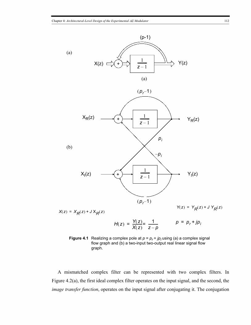
Chapter 4: Architectural-Level Design of the Experimental ΔΣ Modulator 112
1z 1–--------
1z 1–--------
1z 1–--------
+
+
+
(p-1)
p pr jpi+=
X(z) Y(z)
XR(z)
XI(z)
YR(z)
YI(z)
pr 1–( )
pr 1–( )
pi–
pi
Y z( ) YR z( ) J YR z( )+=X z( ) XR z( ) J XR z( )+=
Figure 4.1 Realizing a complex pole at p = pr + jpi using (a) a complex signal flow graph and (b) a two-input two-output real linear signal flow graph.
H z( ) Y z( )X z( )------------ 1
z p–------------==
(a)
(a)
(b)
A mismatched complex filter can be represented with two complex filters. In
Figure 4.2(a), the first ideal complex filter operates on the input signal, and the second, the
image transfer function, operates on the input signal after conjugating it. The conjugation
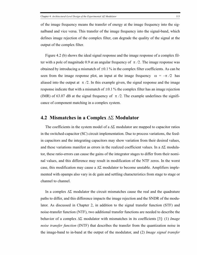
Chapter 4: Architectural-Level Design of the Experimental ΔΣ Modulator 113
of the image frequency means the transfer of energy at the image frequency into the sig-
nalband and vice versa. This transfer of the image frequency into the signal-band, which
defines image rejection of the complex filter, can degrade the quality of the signal at the
output of the complex filter.
Figure 4.2 (b) shows the ideal signal response and the image response of a complex fil-
ter with a pole of magnitude 0.9 at an angular frequency of π 2⁄ . The image response was
obtained by introducing a mismatch of 0.1± % in the complex filter coefficients. As can be
seen from the image response plot, an input at the image frequency ω π– 2⁄= has
aliased into the output at π 2⁄ . In this example given, the signal response and the image
response indicate that with a mismatch of 0.1± % the complex filter has an image rejection
(IMR) of 63.07 dB at the signal frequency of π 2⁄ . The example underlines the signifi-
cance of component matching in a complex system.
4.2 Mismatches in a Complex ΔΣ Modulator
The coefficients in the system model of a ΔΣ modulator are mapped to capacitor ratios
in the switched-capacitor (SC) circuit implementation. Due to process variations, the feed-
in capacitors and the integrating capacitors may show variation from their desired values,
and these variations manifest as errors in the realized coefficient values. In a ΔΣ modula-
tor, these ratio-errors can cause the gains of the integrator stages to differ from their nomi-
nal values, and this difference may result in modification of the NTF zeros. In the worst
case, this modification may cause a ΔΣ modulator to become unstable. Amplifiers imple-
mented with opamps also vary in dc gain and settling characteristics from stage to stage or
channel to channel.
In a complex ΔΣ modulator the circuit mismatches cause the real and the quadrature
paths to differ, and this difference impacts the image rejection and the SNDR of the modu-
lator. As discussed in Chapter 2, in addition to the signal transfer function (STF) and
noise-transfer function (NTF), two additional transfer functions are needed to describe the
behavior of a complex ΔΣ modulator with mismatches in its coefficients [3]: (1) Image
noise transfer function (INTF) that describes the transfer from the quantization noise in
the image-band to in-band at the output of the modulator, and (2) Image signal transfer
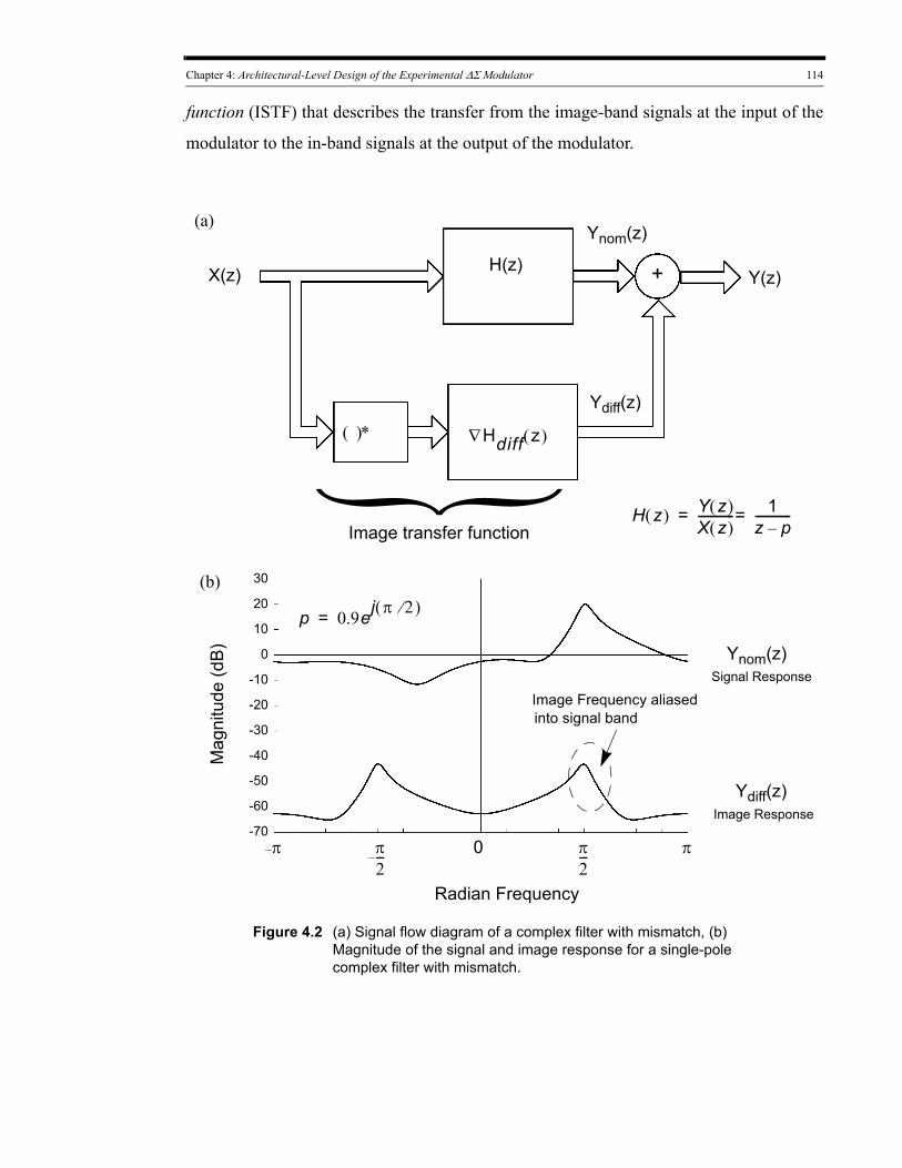
Chapter 4: Architectural-Level Design of the Experimental ΔΣ Modulator 114
function (ISTF) that describes the transfer from the image-band signals at the input of the
modulator to the in-band signals at the output of the modulator.
X(z) Y(z)+
( )∗
H(z)
∇Hdiff z( )
Ynom(z)
Ydiff(z)}Image transfer function
H z( ) Y z( )X z( )------------ 1
z p–------------==
Figure 4.2 (a) Signal flow diagram of a complex filter with mismatch, (b) Magnitude of the signal and image response for a single-pole complex filter with mismatch.
π2--- ππ
2---–π–
-30
30
20
10
0
Mag
nitu
de (d
B)
-20
-10
0
-40
Signal Response
p 0.9ej π 2⁄( )=
Image Response
Image Frequency aliased into signal band
Ynom(z)
Ydiff(z)
Radian Frequency
-50
-60
-70
(a)
(b)
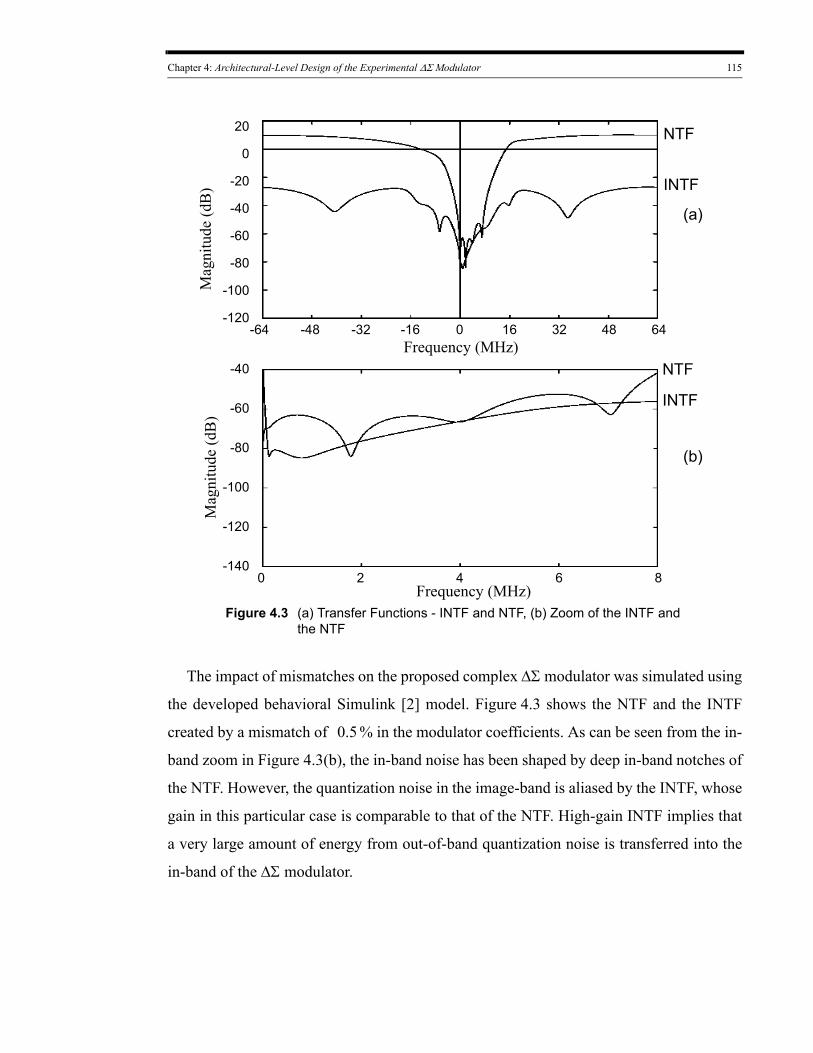
Chapter 4: Architectural-Level Design of the Experimental ΔΣ Modulator 115
Figure 4.3 (a) Transfer Functions - INTF and NTF, (b) Zoom of the INTF and the NTF
-60
-80
-100
-120
-20
-40
0 64-64 32-32 16 48-16-48
Mag
nitu
de (d
B)
-140
-120
-100
-80
-60
-40
Frequency (MHz)
Mag
nitu
de (d
B)
0 842 6
(b)
(a)
0
20
Frequency (MHz)
NTF
INTF
NTF
INTF
The impact of mismatches on the proposed complex ΔΣ modulator was simulated using
the developed behavioral Simulink [2] model. Figure 4.3 shows the NTF and the INTF
created by a mismatch of 0.5 % in the modulator coefficients. As can be seen from the in-
band zoom in Figure 4.3(b), the in-band noise has been shaped by deep in-band notches of
the NTF. However, the quantization noise in the image-band is aliased by the INTF, whose
gain in this particular case is comparable to that of the NTF. High-gain INTF implies that
a very large amount of energy from out-of-band quantization noise is transferred into the
in-band of the ΔΣ modulator.
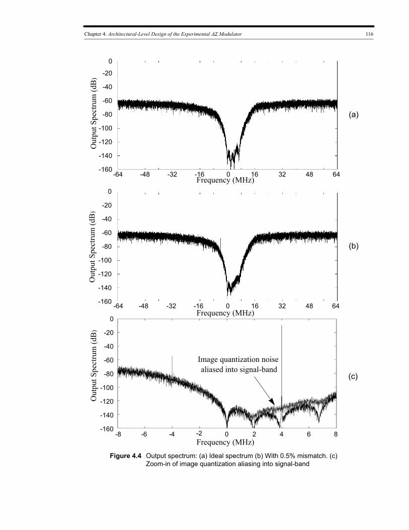
Chapter 4: Architectural-Level Design of the Experimental ΔΣ Modulator 116
-20
-40
-60
-80
-100
Out
put S
pect
rum
(dB
)
0
-120
-140
-160
Figure 4.4 Output spectrum: (a) Ideal spectrum (b) With 0.5% mismatch. (c) Zoom-in of image quantization aliasing into signal-band
Frequency (MHz)
Frequency (MHz)
6432 48160-16-32-48-64
-20
-40
-60
-80
-100
0
-120
-140
-1606432 48160-16-32-48-64
-20
-40
-60
-80
-100
0
-120
-140
-16084 620-2-4-6-8
Out
put S
pect
rum
(dB
)
Frequency (MHz)
Out
put S
pect
rum
(dB
)
Image quantization noise aliased into signal-band
(a)
(b)
(c)
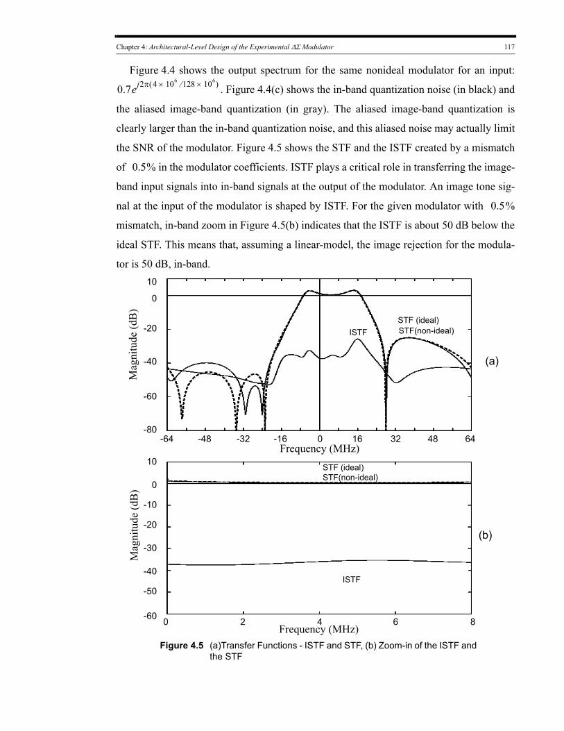
Chapter 4: Architectural-Level Design of the Experimental ΔΣ Modulator 117
Figure 4.4 shows the output spectrum for the same nonideal modulator for an input:
0.7ej2π 4 106× 128 106×⁄( ) . Figure 4.4(c) shows the in-band quantization noise (in black) and
the aliased image-band quantization (in gray). The aliased image-band quantization is
clearly larger than the in-band quantization noise, and this aliased noise may actually limit
the SNR of the modulator. Figure 4.5 shows the STF and the ISTF created by a mismatch
of 0.5% in the modulator coefficients. ISTF plays a critical role in transferring the image-
band input signals into in-band signals at the output of the modulator. An image tone sig-
nal at the input of the modulator is shaped by ISTF. For the given modulator with 0.5%
mismatch, in-band zoom in Figure 4.5(b) indicates that the ISTF is about 50 dB below the
ideal STF. This means that, assuming a linear-model, the image rejection for the modula-
tor is 50 dB, in-band
Figure 4.5 (a)Transfer Functions - ISTF and STF, (b) Zoom-in of the ISTF and the STF
-20
-40
-60
-80
10
0
0 64-64 32-32 16 48-16-48
Mag
nitu
de (d
B)
Frequency (MHz)
-60
-50
-40
-30
-20
-10
0
10
Frequency (MHz)
Mag
nitu
de (d
B)
0 842 6
ISTF
(b)
(a)
STF (ideal)STF(non-ideal)
ISTFSTF (ideal)STF(non-ideal)
.
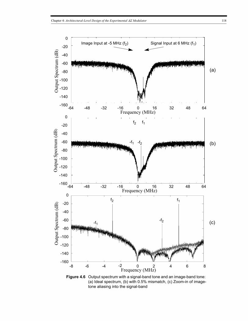
Chapter 4: Architectural-Level Design of the Experimental ΔΣ Modulator 118
-20
-40
-60
-80
-100
Out
put S
pect
rum
(dB
)
0
-120
-140
-160
Figure 4.6 Output spectrum with a signal-band tone and an image-band tone: (a) Ideal spectrum, (b) with 0.5% mismatch, (c) Zoom-in of image-tone aliasing into the signal-band
Frequency (MHz)6432 48160-16-32-48-64
-20
-40
-60
-80
-100
0
-120
-140
-1606432 48160-16-32-48-64
-20
-40
-60
-80
-100
0
-120
-140
-16084 620-2-4-6-8
Out
put S
pect
rum
(dB
)O
utpu
t Spe
ctru
m (d
B)
Frequency (MHz)
Frequency (MHz)
Signal Input at 6 MHz (f1)Image Input at -5 MHz (f2)
(a)
(b)
(c)
f1f2
-f1 -f2
f1f2
-f2-f1
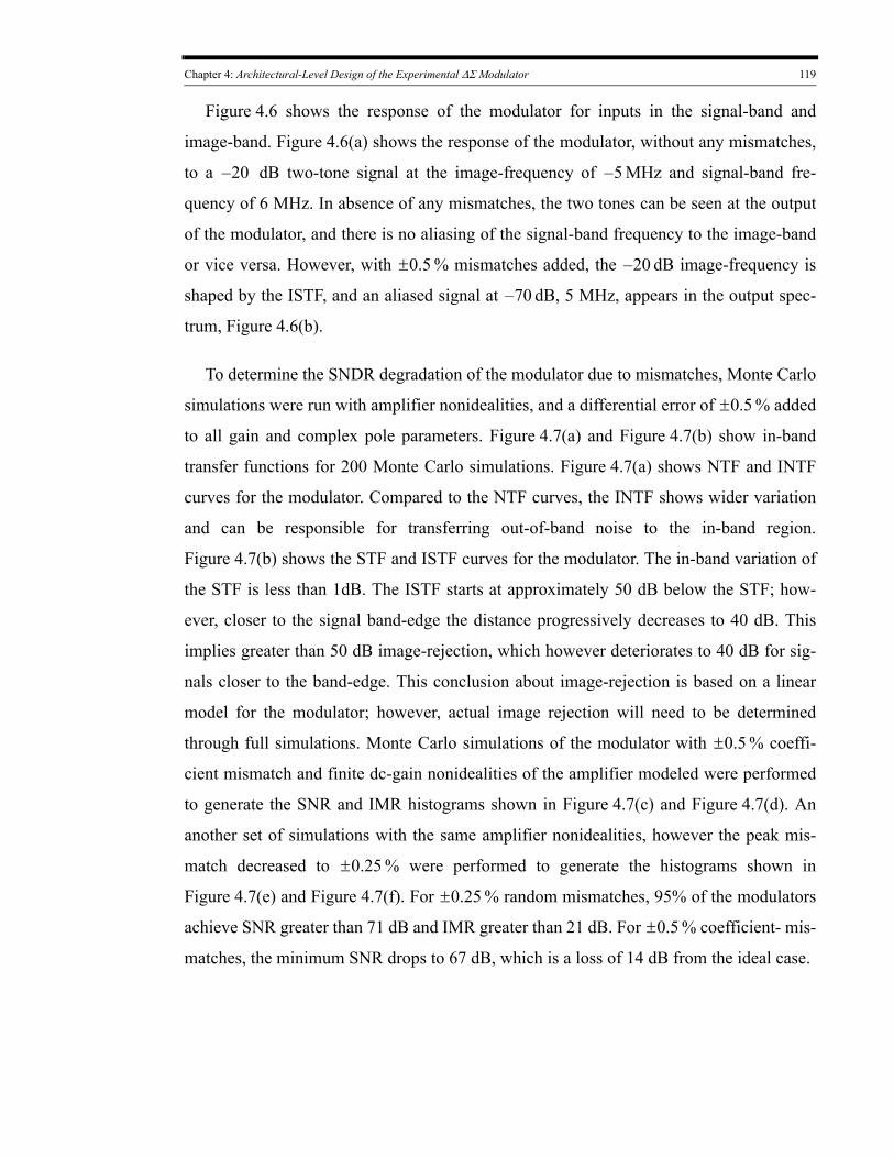
Chapter 4: Architectural-Level Design of the Experimental ΔΣ Modulator 119
Figure 4.6 shows the response of the modulator for inputs in the signal-band and
image-band. Figure 4.6(a) shows the response of the modulator, without any mismatches,
to a 20– dB two-tone signal at the image-frequency of 5– MHz and signal-band fre-
quency of 6 MHz. In absence of any mismatches, the two tones can be seen at the output
of the modulator, and there is no aliasing of the signal-band frequency to the image-band
or vice versa. However, with 0.5± % mismatches added, the 20– dB image-frequency is
shaped by the ISTF, and an aliased signal at 70– dB, 5 MHz, appears in the output spec-
trum, Figure 4.6(b).
To determine the SNDR degradation of the modulator due to mismatches, Monte Carlo
simulations were run with amplifier nonidealities, and a differential error of 0.5± % added
to all gain and complex pole parameters. Figure 4.7(a) and Figure 4.7(b) show in-band
transfer functions for 200 Monte Carlo simulations. Figure 4.7(a) shows NTF and INTF
curves for the modulator. Compared to the NTF curves, the INTF shows wider variation
and can be responsible for transferring out-of-band noise to the in-band region.
Figure 4.7(b) shows the STF and ISTF curves for the modulator. The in-band variation of
the STF is less than 1dB. The ISTF starts at approximately 50 dB below the STF; how-
ever, closer to the signal band-edge the distance progressively decreases to 40 dB. This
implies greater than 50 dB image-rejection, which however deteriorates to 40 dB for sig-
nals closer to the band-edge. This conclusion about image-rejection is based on a linear
model for the modulator; however, actual image rejection will need to be determined
through full simulations. Monte Carlo simulations of the modulator with 0.5± % coeffi-
cient mismatch and finite dc-gain nonidealities of the amplifier modeled were performed
to generate the SNR and IMR histograms shown in Figure 4.7(c) and Figure 4.7(d). An
another set of simulations with the same amplifier nonidealities, however the peak mis-
match decreased to 0.25± % were performed to generate the histograms shown in
Figure 4.7(e) and Figure 4.7(f). For 0.25± % random mismatches, 95% of the modulators
achieve SNR greater than 71 dB and IMR greater than 21 dB. For 0.5± % coefficient- mis-
matches, the minimum SNR drops to 67 dB, which is a loss of 14 dB from the ideal case.
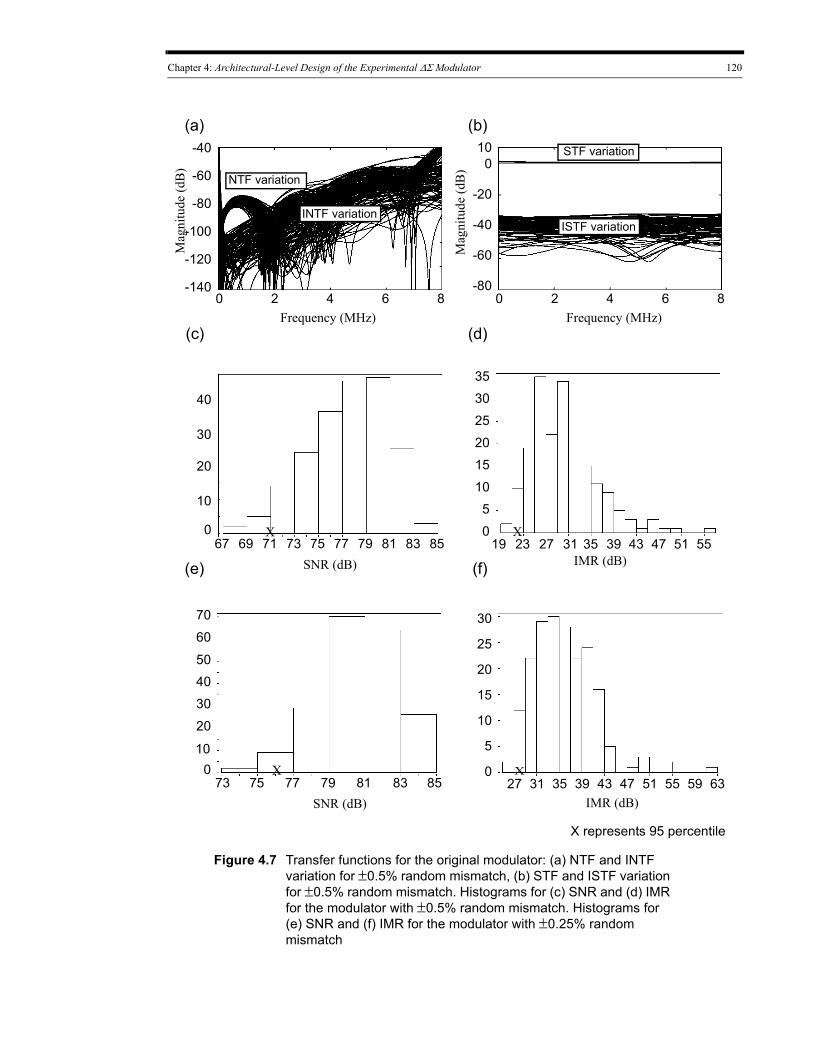
Chapter 4: Architectural-Level Design of the Experimental ΔΣ Modulator 120
Figure 4.7 Transfer functions for the original modulator: (a) NTF and INTF variation for ±0.5% random mismatch, (b) STF and ISTF variation for ±0.5% random mismatch. Histograms for (c) SNR and (d) IMR for the modulator with ±0.5% random mismatch. Histograms for (e) SNR and (f) IMR for the modulator with ±0.25% random mismatch
(a) (b)
0 82 4 6
100
-20
-40
-60
-80
Frequency (MHz)
Mag
nitu
de (d
B)
-40
-60
-80
-100
-120
-140
Mag
nitu
de (d
B)
0 82 4 6Frequency (MHz)
ISTF variation INTF variation ISTF variation
0
10
20
30
40
67 69 71 73 75 77 79 81 83 85SNR (dB)
X
X
73 75 77 79 81 83 850
10
20
30
4050
60
70
X
SNR (dB)
0
5
10
15
20
25
30
IMR (dB)27 31 35 39 43 47 51 55 59 63
(c) (d)
(e) (f) IMR (dB)
0
5
10
15
20
25
30
35
19 23 27 31 35 39 43 47 51 55X
NTF variation
STF variation
X represents 95 percentile
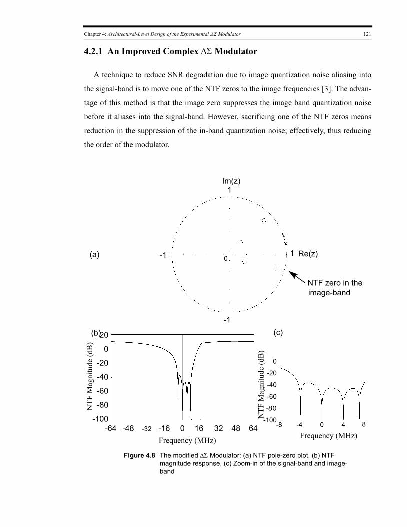
Chapter 4: Architectural-Level Design of the Experimental ΔΣ Modulator 121
4.2.1 An Improved Complex ΔΣ Modulator
A technique to reduce SNR degradation due to image quantization noise aliasing into
the signal-band is to move one of the NTF zeros to the image frequencies [3]. The advan-
tage of this method is that the image zero suppresses the image band quantization noise
before it aliases into the signal-band. However, sacrificing one of the NTF zeros means
reduction in the suppression of the in-band quantization noise; effectively, thus reducing
the order of the modulator.
Figure 4.8 The modified ΔΣ Modulator: (a) NTF pole-zero plot, (b) NTF magnitude response, (c) Zoom-in of the signal-band and image-band
-20
-40
-60
-80
-100
20
NTF
Mag
nitu
de (d
B)
0
-20
-40
-60
-80
-100
0
Frequency (MHz)0 64-64 32-32 -16-48 0 4 8-4-8
(a) 1-1
1
-1
Im(z)
Re(z)0
NTF zero in the image-band
Frequency (MHz)
NTF
Mag
nitu
de (d
B)
(b) (c)
4816
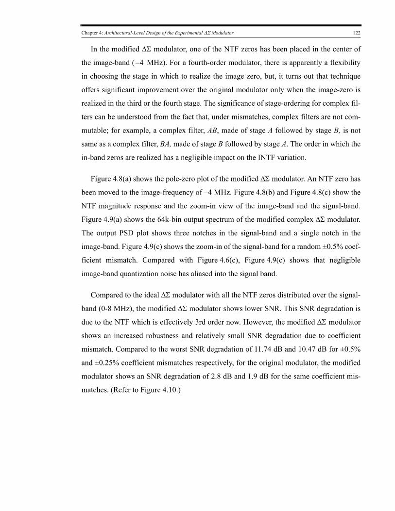
Chapter 4: Architectural-Level Design of the Experimental ΔΣ Modulator 122
In the modified ΔΣ modulator, one of the NTF zeros has been placed in the center of
the image-band ( 4– MHz). For a fourth-order modulator, there is apparently a flexibility
in choosing the stage in which to realize the image zero, but, it turns out that technique
offers significant improvement over the original modulator only when the image-zero is
realized in the third or the fourth stage. The significance of stage-ordering for complex fil-
ters can be understood from the fact that, under mismatches, complex filters are not com-
mutable; for example, a complex filter, AB, made of stage A followed by stage B, is not
same as a complex filter, BA, made of stage B followed by stage A. The order in which the
in-band zeros are realized has a negligible impact on the INTF variation.
Figure 4.8(a) shows the pole-zero plot of the modified ΔΣ modulator. An NTF zero has
been moved to the image-frequency of –4 MHz. Figure 4.8(b) and Figure 4.8(c) show the
NTF magnitude response and the zoom-in view of the image-band and the signal-band.
Figure 4.9(a) shows the 64k-bin output spectrum of the modified complex ΔΣ modulator.
The output PSD plot shows three notches in the signal-band and a single notch in the
image-band. Figure 4.9(c) shows the zoom-in of the signal-band for a random ±0.5% coef-
ficient mismatch. Compared with Figure 4.6(c), Figure 4.9(c) shows that negligible
image-band quantization noise has aliased into the signal band.
Compared to the ideal ΔΣ modulator with all the NTF zeros distributed over the signal-
band (0-8 MHz), the modified ΔΣ modulator shows lower SNR. This SNR degradation is
due to the NTF which is effectively 3rd order now. However, the modified ΔΣ modulator
shows an increased robustness and relatively small SNR degradation due to coefficient
mismatch. Compared to the worst SNR degradation of 11.74 dB and 10.47 dB for ±0.5%
and ±0.25% coefficient mismatches respectively, for the original modulator, the modified
modulator shows an SNR degradation of 2.8 dB and 1.9 dB for the same coefficient mis-
matches. (Refer to Figure 4.10.)
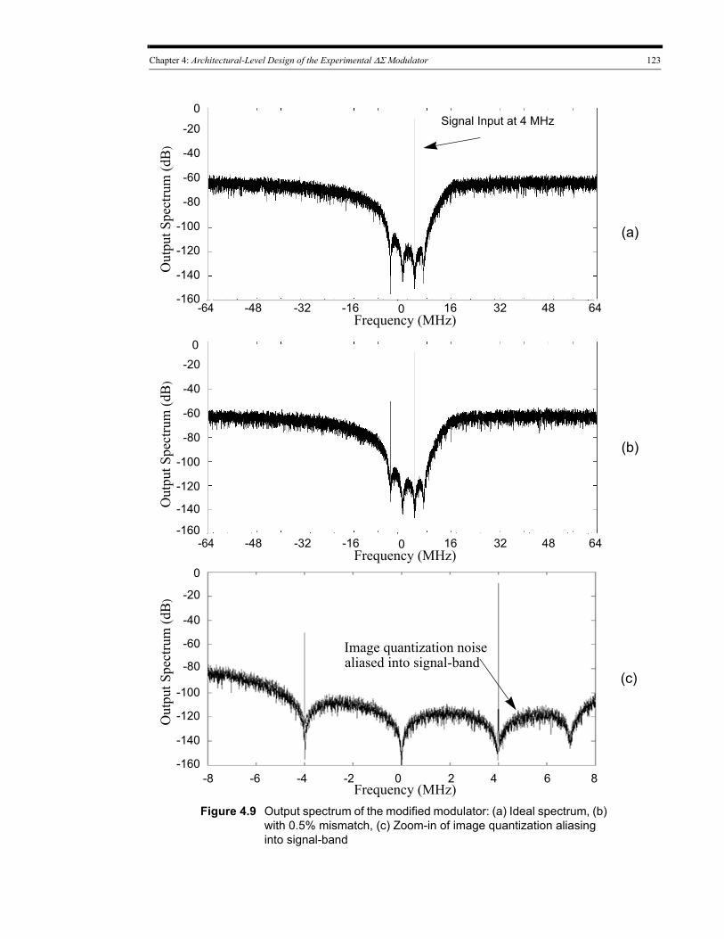
Chapter 4: Architectural-Level Design of the Experimental ΔΣ Modulator 123
-20
-40
-60
-80
-100
0
-120
-140
Frequency (MHz)6432 4816-16-32-48-64
-20
-40
-60
-80
-100
-120
-20
-40
-60
-80
-100
0
-120
-140
-16084 60-2-4-6-8
Out
put S
pect
rum
(dB
)O
utpu
t Spe
ctru
m (d
B)
Frequency (MHz)
Signal Input at 4 MHz
(a)
(b)
(c)
-160
0
-140
-160
0
Frequency (MHz)6432 4816-16-32-48-64 0
2
Out
put S
pect
rum
(dB
)
Figure 4.9 Output spectrum of the modified modulator: (a) Ideal spectrum, (b) with 0.5% mismatch, (c) Zoom-in of image quantization aliasing into signal-band
Image quantization noise aliased into signal-band
Chapter 4: Architectural-Level Design of the Experimental ΔΣ Modulator 124
76 77 78
5
152025
SNR (dB)75
10
3035
0
Figure 4.10 Transfer functions for the modified modulator: (a) NTF and INTF variation for ±0.5% random mismatch, (b) STF and ISTF variation for ±0.5% random mismatch. Histograms for (c) SNR and (d) IMR for the modulator with ±0.5% random mismatch. Histograms for (e) SNR and (f) IMR for the modulator with ±0.25% random mismatch
IMR (dB)
5
10
15
20
25
30
22 26 30 34 38 42 46 50X0
5
101520
25
30
0
IMR (dB)25 29 33 37 41 45 49 53
35
57X
0 82 4 6
100
-20
-40
-60
-80
Frequency (MHz)
Mag
nitu
de (d
B)
-40
-60
-80
-100
-120
-140
Mag
nitu
de (d
B)
0 82 4 6
STF variation
Frequency (MHz)
ISTF variation INTF variation
X
(a) (b)
(c) (d)
(e) (f)
76 77 78
5
10
15
20
SNR (dB)
0 X
NTF variation
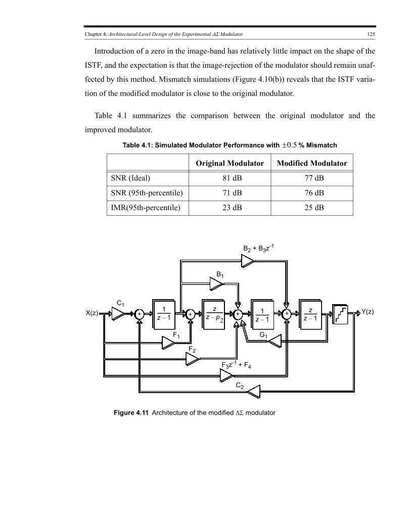
Chapter 4: Architectural-Level Design of the Experimental ΔΣ Modulator 125
Introduction of a zero in the image-band has relatively little impact on the shape of the
ISTF, and the expectation is that the image-rejection of the modulator should remain unaf-
fected by this method. Mismatch simulations (Figure 4.10(b)) reveals that the ISTF varia-
tion of the modified modulator is close to the original modulator.
Table 4.1 summarizes the comparison between the original modulator and the
improved modulator.
Table 4.1: Simulated Modulator Performance with 0.5± % Mismatch
Original Modulator Modified Modulator
SNR (Ideal) 81 dB 77 dB
SNR (95th-percentile) 71 dB 76 dB
IMR(95th-percentile) 23 dB 25 dB
F3z-1 + F4
F2
F1
B1
B2 + B3z-1
1z 1–------------ z
z p2–---------------
C2
C1X(z) Y(z)1
z 1–------------
zz 1–------------
G1
Figure 4.11 Architecture of the modified ΔΣ modulator
++++
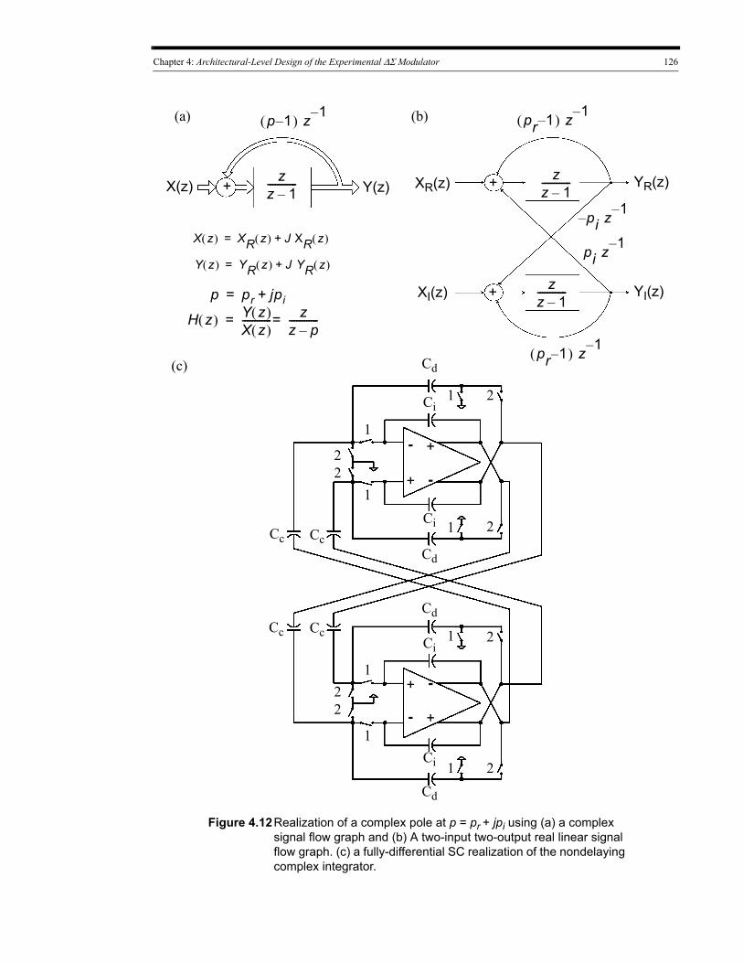
Chapter 4: Architectural-Level Design of the Experimental ΔΣ Modulator 126
zz 1–------------z
z 1–------------
zz 1–------------
+
+
+
p pr jpi+=
X(z) Y(z) XR(z)
XI(z)
YR(z)
YI(z)
p 1–( ) z 1–
pi z1–
Y z( ) YR z( ) J YR z( )+=
X z( ) XR z( ) J XR z( )+=
Figure 4.12Realization of a complex pole at p = pr + jpi using (a) a complex signal flow graph and (b) A two-input two-output real linear signal flow graph. (c) a fully-differential SC realization of the nondelaying complex integrator.
H z( ) Y z( )X z( )------------ z
z p–------------==
(a) (b)
pi– z 1–
pr 1–( ) z 1–
pr 1–( ) z 1–(c)
1
1
1
1
2
2
1
1
2
2
1
1
22
22
Ci
CcCc
CcCc
Ci
Cd
Ci
Cd
Cd
Ci
Cd
+
+
+
+
-
-
-
-
Chapter 4: Architectural-Level Design of the Experimental ΔΣ Modulator 127
4.3 The Switched-Capacitor Architecture
4.3.1 Complex Integrators
A complex integrator is created by two cross-coupled real integrators, as shown in
Figure 4.12. The nondelaying complex integrator of the proposed ΔΣ modulator has been
realized by two non-delaying SC integrators. As the SC implementation is fully-differen-
tial, the negative valued cross-coupling coefficient is realized by reversing the connection
to the differential amplifier outputs. The ratio of the feedback capacitor, Cd, to the integra-
tion capacitor, Ci, sets the real part of the complex zero, and the ratio of Cd to Ci sets the
imaginary part of the complex zero.
4.3.2 Dynamic Range Scaling
For an SC modulator, the voltage swing at an integrator output is limited by the output
saturation voltages of the opamps. The ΔΣ modulator Simulink model was simulated for
different input frequencies and amplitudes in order to obtain the peak values at each inte-
grator output. To ensure that each opamp output never exceeded the reference levels,
dynamic range scaling was performed by multiplying the coefficients at an integrator
input by a factor and dividing the coefficients at the output of the integrator by the same
factor [1]. In the Simulink model, for a –6 dB input signal, the peak values at the integrator
outputs were limited to 70% of the reference levels.
The reference levels to the multibit quantizer and the multilevel DAC are set at 1.4 V
and 0.4 V, and centered around a common-mode of 0.9 V. With Dynamic range scaling,
each opamp is limited to a maximum differential swing of 1.4 Vp-p.
4.3.3 Multibit Quantization
During the noise assignment of the modulator (see Section 4.4.1.2) , 25% of the total
permissible noise was assigned to in-band quantization noise. At an OSR of 16, a 4-bit
quantizer is required to suppress the in-band quantization-noise to the required level that
is, below the noises from the analog circuit and other sources. Behavioral simulations with
Chapter 4: Architectural-Level Design of the Experimental ΔΣ Modulator 128
a 4-bit quantizer predict a peak signal-to-quantization ratio (SQNRpeak) of 81 dB for an
overload-ratio (AOL) [4] of 0.75.
In the proposed ΔΣ modulator implementation, the 4-bit quantizer will be implemented
as a 15-level flash ADC. Behavioral Monte Carlo simulations show that the modulator is
robust to quantizer offsets, and even an offset of value 20 mV has a negligible impact on
the SNR of the modulator.
4.3.4 Multilevel DAC
The proposed complex ΔΣ modulator uses one multilevel DAC in the feedback loop.
The complex feedback coefficient, C2, in Figure 4.11 is realized by a real and an imagi-
nary array of 15 capacitors each. The thermometer output code of the quantizer is con-
nected to the switched-capacitor feedback DAC. To account for the effect of capacitor
mismatches in the DAC unit capacitors, the behavioral model of the modulator was simu-
lated with mismatch error in the DAC elements. Section 4.4.1 reports the worst-case
SNDR performance due multilevel DAC nonlinearity found over 100 simulations of the
modulator.
4.3.5 Realizing the Feedins
In Figure 4.11, the coefficient F3 realizes an input feed-in term delayed by one clock
cycle before it is added to other inputs of the last integrator. To implement F3, the com-
bined feed-in terms F3 and F4 were implemented as the summation of a nondelayed term
and a differentiator term:
F3z 1– F4 F3 F4 F3 1 z 1––( )–+=+
Similarly, to reduce the coefficient spread for the coefficients B2 and B3, the feed-for-
ward B2 + B3 z-1 was implemented as:
B2 B3z 1– B2 B3 B3 1 z 1––( )–+=+
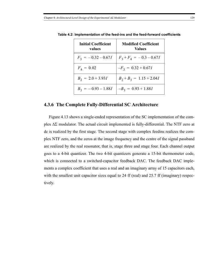
Chapter 4: Architectural-Level Design of the Experimental ΔΣ Modulator 129
Table 4.2: Implementation of the feed-ins and the feed-forward coefficients
Initial Coefficient values
Modified Coefficient Values
F3 0.32– 0.67I–= F3 F4+ 0.3– 0.67I–=
F4 0.02= F– 3 0.32 0.67I+=
B2 2.0 3.93I+= B2 B3+ 1.15 2.04I+=
B3 0.93– 1.88I–= B– 3 0.93 1.88I+=
4.3.6 The Complete Fully-Differential SC Architecture
Figure 4.13 shows a single-ended representation of the SC implementation of the com-
plex ΔΣ modulator. The actual circuit implemented is fully-differential. The NTF zero at
dc is realized by the first stage. The second stage with complex feedins realizes the com-
plex NTF zero, and the zeros at the image frequency and the centre of the signal passband
are realized by the real resonator, that is, stage three and stage four. Each channel output
goes to a 4-bit quantizer. The two 4-bit quantizers generate a 15-bit thermometer code,
which is connected to a switched-capacitor feedback DAC. The feedback DAC imple-
ments a complex coefficient that uses a real and an imaginary array of 15 capacitors each,
with the smallest unit capacitor sizes equal to 24 ff (real) and 25.7 ff (imaginary) respec-
tively.
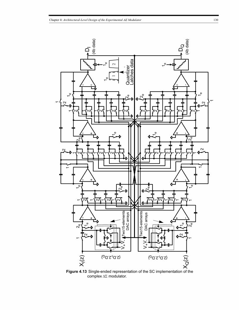
Chapter 4: Architectural-Level Design of the Experimental ΔΣ Modulator 130
Figure 4.13 Single-ended representation of the SC implementation of the complex ΔΣ modulator.
X I(z
)
XQ
(z)
DI
DQ
V+V
-1
21 e
1
{2.DI,2.DQ}
2 e-
--
-
-
+
12
21
2 e
211 2 1 1 222 1
1 e
1 e
1
{2.DI,2.DQ}
Qua
ntiz
erLa
tche
s da
ta
2 e
2
2
1 e
1
Two1
5-el
emen
tsD
AC
arra
ys
Two1
5-el
emen
tsD
AC
arr
ays
2 e+
+
+
+
2
1 2 1 2 2 1 2 11 e
1 2 1 2 1
1 2 1 12
1 e
2 1 2 1
2
1-
+
+
--
1
1 e
2 21212122 e
2
2
12 e
2
(4b
data
)
(4b
data
)
1 e
11 e
2 1 2 1 2 1 2 1 2
2 e
1
V+V
-
1
+
1 e2 e
1 e
Chapter 4: Architectural-Level Design of the Experimental ΔΣ Modulator 131
4.3.7 The Clocking Scheme
The ΔΣ ADC uses two non-overlapping clock phases, φ1 and φ2 , and their ‘‘early”
versions, φ1e and φ2e , to minimize charge-injection [5]. A nonoverlapping clock genera-
tor provides the necessary clock phases.
The first stage of the modulator samples input during clock phase φ1 , and the feedback
DAC applies the references during clock phase φ2 . Figure 4.14 shows the fully-differen-
tial implementation and clocking for the fourth-stage amplifier and the 4-bit quantizer.
Figure 4.14 Clocking scheme- real-channel fourth-stage and the quantizer.
DI (4b data)
φ1
φ1e
-
Iop1Qon1
1
11111
11111
IpQn
QpInQop1Ion1
2 2 2
2
2 2
2 2 2 2
2
2
1
1
Iop3Iop1Qon1InQp
+
VcmiVcmo
In
Ion1Ion3
Qn
φ1
φ2
φ1e
φ1e
Iop4
Ion4
(to third stage)
Qop1
Chapter 4: Architectural-Level Design of the Experimental ΔΣ Modulator 132
4.4 System-level Behavioral Simulations
4.4.1 Capacitor Sizing
4.4.1.1 Capacitor Mismatch
In an SC ΔΣ modulator, the integrator gains are implemented by capacitor ratios. Pro-
cess variations cause the realized capacitors to deviate from their nominal values. For
example, for a coefficient of value G realized as a ratio of two capacitors, Cg and Ci, the
actual implemented coefficient value, G*, is given by:
G∗
Cg 1Ac
m WL( )g
------------------------+⎝ ⎠⎜ ⎟⎛ ⎞
Ci 1Ac
n WL( )i
----------------------+⎝ ⎠⎜ ⎟⎛ ⎞
----------------------------------------------= (4.1)
where Ac is a process-dependent parameter1. The deviations of the coefficients from their
nominal values are manifest as a modification of the NTF and STF of the modulator. A
technique intended to realize capacitor ratios with higher accuracy is implementation by
capacitors realized as an array of unit capacitors. Behavioral simulations of the modulator
were used to identify the sensitive coefficients, and the capacitors realizing these
coefficients were sized larger in order to minimize their deviations.
The multilevel DAC has been implemented as an array of unit capacitors. Errors in the
values of these unit capacitors can limit the linearity and resolution of the ΔΣ modulator.
To account for the effect of capacitor mismatches in the DAC unit capacitors, over 100
behavioral simulations, with random mismatches of 0.5± % peak-value in the DAC unit
elements, were performed to examine the worst case SNDR and IMR.
For 0.5± % mismatch values, the minimum SNDR falls to 69.7 dB with 95-percentile
at 70 dB. The minimum IMR drops to 46.2 dB, with 95-percentile of the IMR at 48.6 dB.
1. This assumes that the area effects dominate and the edge effects can be ignored.
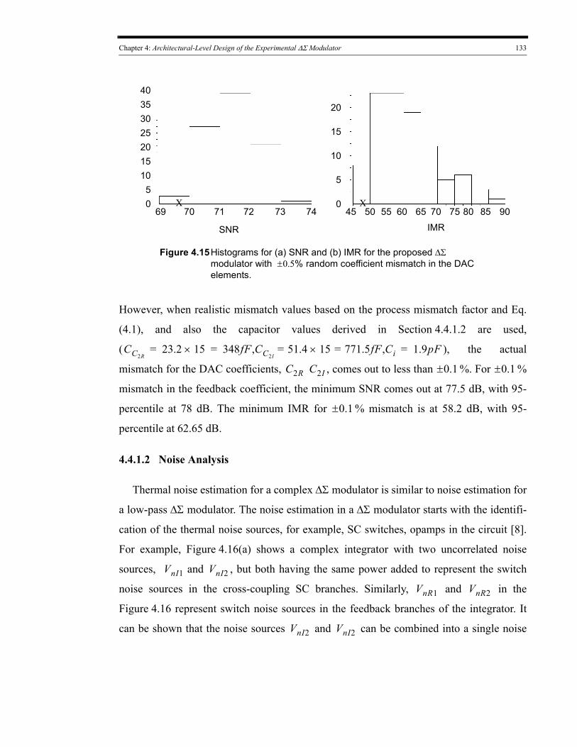
Chapter 4: Architectural-Level Design of the Experimental ΔΣ Modulator 133
5
10
15
20
045 50 55 60 65 70 75 80
Figure 4.15Histograms for (a) SNR and (b) IMR for the proposed ΔΣ modulator with % random coefficient mismatch in the DAC elements.
0.5±
X X85 9069 70 71 72 73 74
05
10152025303540
SNR IMR
However, when realistic mismatch values based on the process mismatch factor and Eq.
(4.1), and also the capacitor values derived in Section 4.4.1.2 are used,
(CC2R23.2 15× 348fF CC2I
51.4 15× 771.5fF Ci,= =, 1.9pF= = = ), the actual
mismatch for the DAC coefficients, C2R C2I , comes out to less than 0.1± %. For 0.1± %
mismatch in the feedback coefficient, the minimum SNR comes out at 77.5 dB, with 95-
percentile at 78 dB. The minimum IMR for 0.1± % mismatch is at 58.2 dB, with 95-
percentile at 62.65 dB.
4.4.1.2 Noise Analysis
Thermal noise estimation for a complex ΔΣ modulator is similar to noise estimation for
a low-pass ΔΣ modulator. The noise estimation in a ΔΣ modulator starts with the identifi-
cation of the thermal noise sources, for example, SC switches, opamps in the circuit [8].
For example, Figure 4.16(a) shows a complex integrator with two uncorrelated noise
sources, VnI1 and VnI2 , but both having the same power added to represent the switch
noise sources in the cross-coupling SC branches. Similarly, VnR1 and VnR2 in the
Figure 4.16 represent switch noise sources in the feedback branches of the integrator. It
can be shown that the noise sources VnI2 and VnI2 can be combined into a single noise
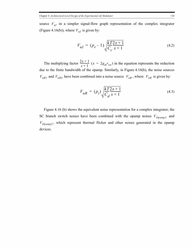
Chapter 4: Architectural-Level Design of the Experimental ΔΣ Modulator 134
source VnI in a simpler signal-flow graph representation of the complex integrator
(Figure 4.16(b)), where VnI is given by:
VnI pr 1–( ) kTCc------2x 1+
x 1+---------------= (4.2)
The multiplying factor 2x 1+x 1+
--------------- (x 2gmron= ) in the equation represents the reduction
due to the finite bandwidth of the opamp. Similarly, in Figure 4.16(b), the noise sources
VnR1 and VnR2 have been combined into a noise source VnR , where VnR is given by:
VnR pi( ) kTCd------2x 1+
x 1+---------------= (4.3)
Figure 4.16 (b) shows the equivalent noise representation for a complex integrator; the
SC branch switch noises have been combined with the opamp noises VOpamp1 and
VOpamp2 , which represent thermal flicker and other noises generated in the opamp
devices.
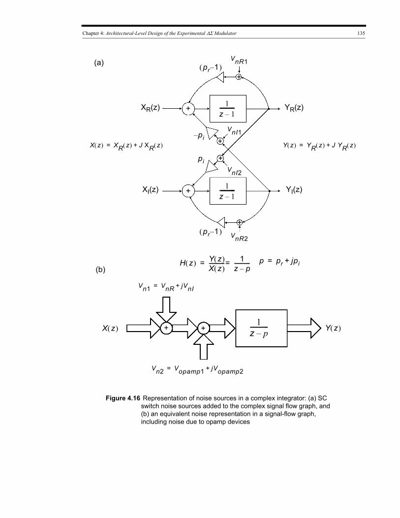
Chapter 4: Architectural-Level Design of the Experimental ΔΣ Modulator 135
1z 1–--------
1z 1–--------
XR(z)
XI(z)
YR(z)
YI(z)
pr 1–( )
pr 1–( )
pi–
pi
Figure 4.16 Representation of noise sources in a complex integrator: (a) SC switch noise sources added to the complex signal flow graph, and (b) an equivalent noise representation in a signal-flow graph, including noise due to opamp devices
+
+
p pr jpi+=
Y z( ) YR z( ) J YR z( )+=X z( ) XR z( ) J XR z( )+=
H z( ) Y z( )X z( )------------ 1
z p–------------==
+
+
+
+
++
VnI2
VnI1
VnR1
VnR2
1z p–------------X z( ) Y z( )
Vn1 VnR jVnI+=
Vn2 Vopamp1 jVopamp2+=
(a)
(b)
Chapter 4: Architectural-Level Design of the Experimental ΔΣ Modulator 136
Figure 4.17Noise sources added to the complex ΔΣ modulator
zz
1–
--------
----+
X(z
)Y
(z)
zz
p–
--------
----1
z1
–-----
-------
1z
1–
--------
----+
++
+
+
+
+
+
+
+
+
+
C1
C2
A 1A 2
A 3
B 1
B 23
(=B 2
-B3)-B
3 (1
-z-1
)
F 2F 3
4 (=
F 3+F
4)
F 1G
1
-F3
(1-z
-1)
+
++
+
+
+
Chapter 4: Architectural-Level Design of the Experimental ΔΣ Modulator 137
Figure 4.17 shows the block diagram of the complex ΔΣ modulator, with thermal noise
sources added at the inputs of the feed-ins to the integrators. For an integrator stage, the
opamp noise after proper scaling can be combined with one of the feed-in noise sources.
Figure 4.18 shows the frequency responses of the power transfer functions for each noise
source to the output of the modulator. For a complex coefficient, there are two transfer
functions corresponding to the real and the imaginary parts of the coefficient. Integration
of each power transfer function from dc to the signal-band edge represents the gain of the
noise source to the output of the modulator. Since the complex ΔΣ modulator has been
designed with a unity STF in the signal-band, the input-referred noise power is equal to
the output-referred noise power.
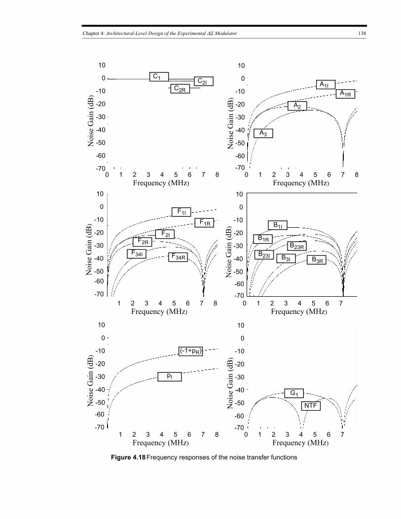
Chapter 4: Architectural-Level Design of the Experimental ΔΣ Modulator 138
C1 C2IC2R
-70 -70
Noi
se G
ain
(dB
)
-60
-50
-40
-30
-20
-10
0
10
0 84 621 3 5 7Frequency (MHz)
A1IA1R
A2
A3
-60
-50
-40
-30
-20
-10
0
10
0 84 621 3 5 7Frequency (MHz)
Noi
se G
ain
(dB
)
F1I
F1R
F2IF2R
F34I F34R
B1R
B1I
B23I
B23R
G1
(-1+pR)
pI
Noi
se G
ain
(dB
)
-50
-40
-30
-20
-10
0
10
84 621 3 5 7Frequency (MHz)
-50
-40
-30
-20
-10
0
10
0 4 621 3 5 7Frequency (MHz)
Noi
se G
ain
(dB
)
Noi
se G
ain
(dB
)
-50
-40
-30
-20
-10
0
10
84 621 3 5 7Frequency (MHz)
-50
-40
-30
-20
-10
0
10
0 4 621 3 5 7Frequency (MHz)
Noi
se G
ain
(dB
)
-70
-60
-70
-60
-70
-60
-70
-60
Figure 4.18Frequency responses of the noise transfer functions
B3RB3I
NTF
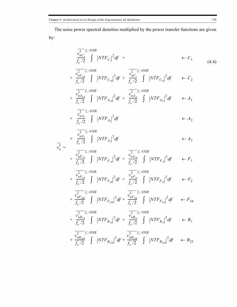
Chapter 4: Architectural-Level Design of the Experimental ΔΣ Modulator 139
The noise power spectral densities multiplied by the power transfer functions are given
by:
vn2
vnC1
2
fs 2⁄---------- NTFC1
2 fd
fs OSR⁄
∫ + C1←
+vnC2R
2
fs 2⁄------------ NTFC2R
2 fd
fs OSR⁄
∫ +vnC1
2
fs 2⁄---------- NTFC2I
2 fd
fs OSR⁄
∫ C2←
+vnA1R
2
fs 2⁄----------- NTFA1R
2 fd
fs OSR⁄
∫ +vnA1I
2
fs 2⁄----------- NTFA1I
2 fd
fs OSR⁄
∫ A1←
+vnA2
2
fs 2⁄---------- NTFA2
2 fd
fs OSR⁄
∫ A2←
+vnA3
2
fs 2⁄---------- NTFA3
2 fd
fs OSR⁄
∫ A3←
+vnF1R
2
fs 2⁄----------- NTFF1R
2 fd
fs OSR⁄
∫ +vnA1R
2
fs 2⁄----------- NTFF1I
2 fd
fs OSR⁄
∫ F1←
+vnF2R
2
fs 2⁄----------- NTFF2R
2 fd
fs OSR⁄
∫ +vnF2I
2
fs 2⁄----------- NTFF2I
2 fd
fs OSR⁄
∫ F2←
+vnF34R
2
fs 2⁄------------- NTFF34R
2 fd
fs OSR⁄
∫ +vnF34I
2
fs 2⁄------------ NTFF34I
2 fd
fs OSR⁄
∫ F34←
+vnB1R
2
fs 2⁄----------- NTFB1R
2 fd
fs OSR⁄
∫ +vnB1I
2
fs 2⁄----------- NTFB1I
2 fd
fs OSR⁄
∫ B1←
+vnB23R
2
fs 2⁄------------- NTFB23R
2 fd
fs OSR⁄
∫ +vnB23R
2
fs 2⁄------------- NTFB23R
2 fd
fs OSR⁄
∫ B23←
=
(4.4)
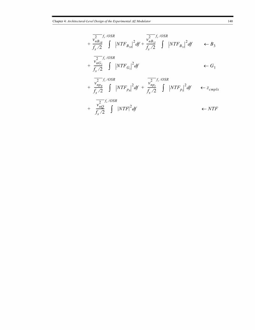
Chapter 4: Architectural-Level Design of the Experimental ΔΣ Modulator 140
+vnB3R
2
fs 2⁄----------- NTFB3R
2 fd
fs OSR⁄
∫ +vnB3I
2
fs 2⁄----------- NTFB3I
2 fd
fs OSR⁄
∫ B3←
+vnG1
2
fs 2⁄---------- NTFG1
2 fd
fs OSR⁄
∫ G1←
+vnpR
2
fs 2⁄---------- NTFpR
2 fd
fs OSR⁄
∫ +vnpI
2
fs 2⁄---------- NTFpI
2 fd
fs OSR⁄
∫ zcmplx←
+vnQ
2
fs 2⁄---------- NTF 2 fd
fs OSR⁄
∫ NTF←
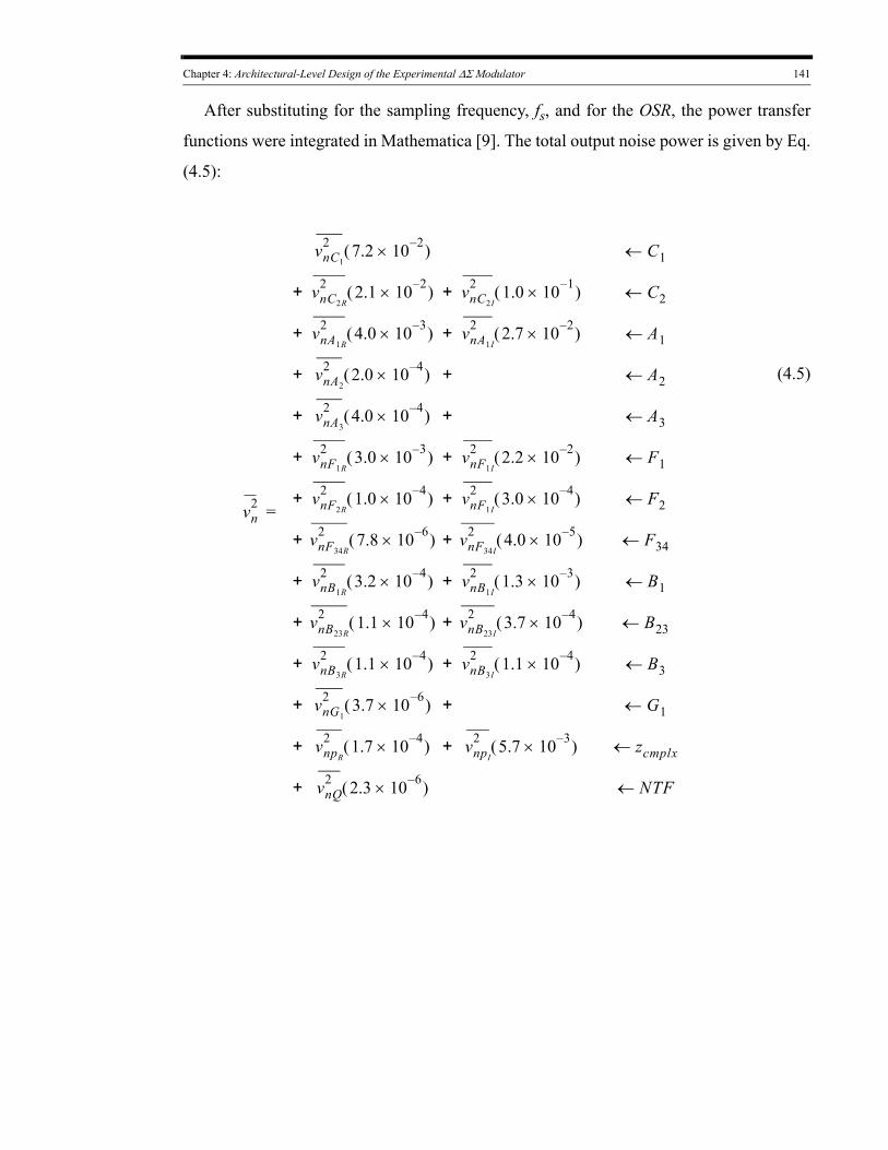
Chapter 4: Architectural-Level Design of the Experimental ΔΣ Modulator 141
After substituting for the sampling frequency, fs, and for the OSR, the power transfer
functions were integrated in Mathematica [9]. The total output noise power is given by Eq.
(4.5):
vn2
vnC1
2 7.2 10 2–×( ) C1←
+ vnC2R
2 2.1 10 2–×( ) + vnC2I
2 1.0 10 1–×( ) C2←
+ vnA1R
2 4.0 10 3–×( ) + vnA1I
2 2.7 10 2–×( ) A1←
+ vnA2
2 2.0 10 4–×( ) + A2←
+ vnA3
2 4.0 10 4–×( ) + A3←
+ vnF1R
2 3.0 10 3–×( ) + vnF1I
2 2.2 10 2–×( ) F1←
+ vnF2R
2 1.0 10 4–×( ) + vnF1I
2 3.0 10 4–×( ) F2←
+ vnF34R
2 7.8 10 6–×( ) + vnF34I
2 4.0 10 5–×( ) F34←
+ vnB1R
2 3.2 10 4–×( ) + vnB1I
2 1.3 10 3–×( ) B1←
+ vnB23R
2 1.1 10 4–×( ) + vnB23I
2 3.7 10 4–×( ) B23←
+ vnB3R
2 1.1 10 4–×( ) + vnB3I
2 1.1 10 4–×( ) B3←
+ vnG1
2 3.7 10 6–×( ) + G1←
+ vnpR
2 1.7 10 4–×( ) + vnpI
2 5.7 10 3–×( ) zcmplx←
+ vnQ2 2.3 10 6–×( ) NTF←
=
(4.5)
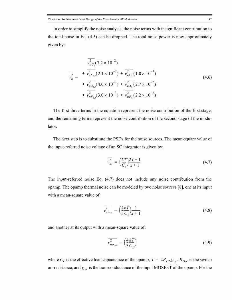
Chapter 4: Architectural-Level Design of the Experimental ΔΣ Modulator 142
In order to simplify the noise analysis, the noise terms with insignificant contribution to
the total noise in Eq. (4.5) can be dropped. The total noise power is now approximately
given by:
vn2
vnC1
2 7.2 10 2–×( )
+ vnC2R
2 2.1 10 2–×( ) + vnC2I
2 1.0 10 1–×( )
+ vnA1R
2 4.0 10 3–×( ) + vnA1I
2 2.7 10 2–×( )
+ vnF1R
2 3.0 10 3–×( ) + vnF1I
2 2.2 10 2–×( )
= (4.6)
The first three terms in the equation represent the noise contribution of the first stage,
and the remaining terms represent the noise contribution of the second stage of the modu-
lator.
The next step is to substitute the PSDs for the noise sources. The mean-square value of
the input-referred noise voltage of an SC integrator is given by:
vni2 kT
Cs------⎝ ⎠
⎛ ⎞ 2x 1+x 1+
---------------= (4.7)
The input-referred noise Eq. (4.7) does not include any noise contribution from the
opamp. The opamp thermal noise can be modeled by two noise sources [8], one at its input
with a mean-square value of:
vniOP
2 43---kT
Cs------⎝ ⎠
⎛ ⎞ 1x 1+------------= (4.8)
and another at its output with a mean-square value of:
vnoOP
2 43--- kT
CL------⎝ ⎠
⎛ ⎞= (4.9)
where CL is the effective load capacitance of the opamp, x 2RONgm= . RON is the switch
on-resistance, and gm is the transconductance of the input MOSFET of the opamp. For the
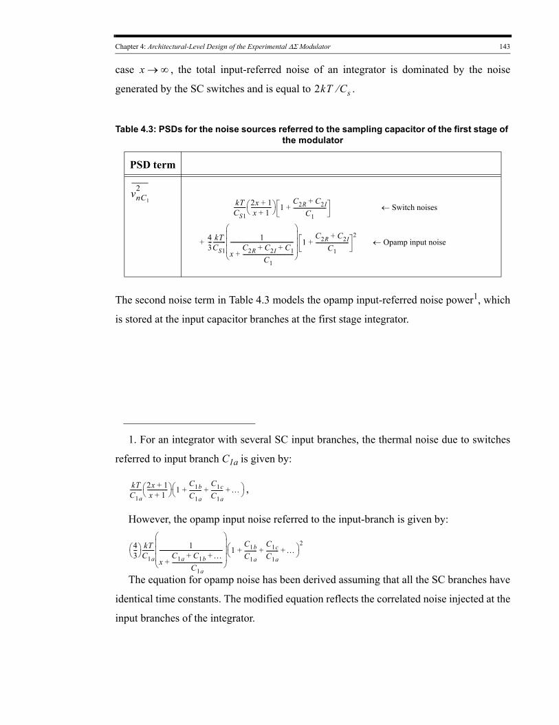
Chapter 4: Architectural-Level Design of the Experimental ΔΣ Modulator 143
case x ∞→ , the total input-referred noise of an integrator is dominated by the noise
generated by the SC switches and is equal to 2kT Cs⁄ .
Table 4.3: PSDs for the noise sources referred to the sampling capacitor of the first stage of the modulator
PSD term
vnC1
2
kTCS1--------- 2x 1+
x 1+---------------⎝ ⎠
⎛ ⎞ 1C2R C2I+
C1------------------------+ Switch noises←
+ 43--- kT
CS1--------- 1
xC2R C2I C1+ +
C1-------------------------------------+
----------------------------------------------
⎝ ⎠⎜ ⎟⎜ ⎟⎜ ⎟⎛ ⎞
1C2R C2I+
C1------------------------+
2Opamp input noise←
The second noise term in Table 4.3 models the opamp input-referred noise power1, which
is stored at the input capacitor branches at the first stage integrator.
1. For an integrator with several SC input branches, the thermal noise due to switches
referred to input branch C1a is given by:
kTC1a--------- 2x 1+
x 1+---------------⎝ ⎠
⎛ ⎞ 1C1bC1a---------
C1cC1a--------- …+ + +⎝ ⎠
⎛ ⎞ ,
However, the opamp input noise referred to the input-branch is given by:
43---⎝ ⎠
⎛ ⎞ kTC1a--------- 1
xC1a C1b …+ +
C1a-------------------------------------+
----------------------------------------------
⎝ ⎠⎜ ⎟⎜ ⎟⎜ ⎟⎛ ⎞
1C1bC1a---------
C1cC1a--------- …+ + +⎝ ⎠
⎛ ⎞ 2
The equation for opamp noise has been derived assuming that all the SC branches have
identical time constants. The modified equation reflects the correlated noise injected at the
input branches of the integrator.
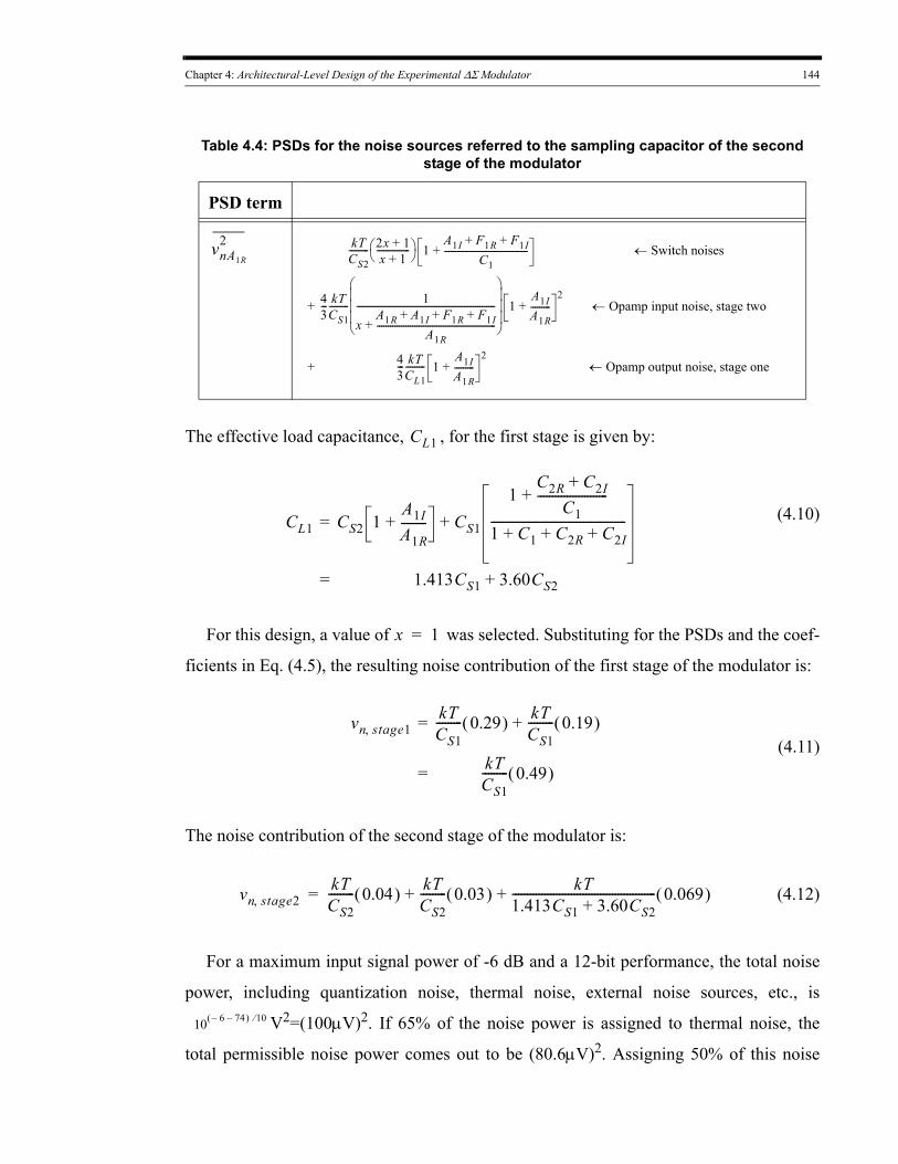
Chapter 4: Architectural-Level Design of the Experimental ΔΣ Modulator 144
Table 4.4: PSDs for the noise sources referred to the sampling capacitor of the second stage of the modulator
PSD term
vnA1R
2 kTCS2--------- 2x 1+
x 1+---------------⎝ ⎠
⎛ ⎞ 1A1I F1R F1I+ +
C1--------------------------------------+ Switch noises←
+ 43--- kT
CS1--------- 1
xA1R A1I F1R F1I+ + +
A1R------------------------------------------------------+
---------------------------------------------------------------
⎝ ⎠⎜ ⎟⎜ ⎟⎜ ⎟⎛ ⎞
1A1IA1R---------+
2Opamp input noise, stage two←
+ 43--- kT
CL1--------- 1
A1IA1R---------+
2Opamp output noise, stage one←
The effective load capacitance, CL1 , for the first stage is given by:
CL1 = CS2 1A1IA1R---------+ CS1
1C2R C2I+
C1------------------------+
1 C1 C2R C2I+ + +----------------------------------------------+
= 1.413CS1 3.60CS2+
(4.10)
For this design, a value of x 1= was selected. Substituting for the PSDs and the coef-
ficients in Eq. (4.5), the resulting noise contribution of the first stage of the modulator is:
vn stage1, = kTCS1--------- 0.29( ) kT
CS1--------- 0.19( )+
= kTCS1--------- 0.49( )
(4.11)
The noise contribution of the second stage of the modulator is:
vn stage2,kTCS2--------- 0.04( ) kT
CS2--------- 0.03( ) kT
1.413CS1 3.60CS2+------------------------------------------------- 0.069( )+ += (4.12)
For a maximum input signal power of -6 dB and a 12-bit performance, the total noise
power, including quantization noise, thermal noise, external noise sources, etc., is
10 6– 74–( ) 10⁄ V2=(100μV)2. If 65% of the noise power is assigned to thermal noise, the
total permissible noise power comes out to be (80.6μV)2. Assigning 50% of this noise
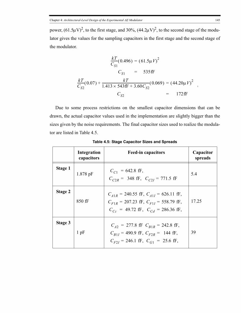
Chapter 4: Architectural-Level Design of the Experimental ΔΣ Modulator 145
power, (61.5μV)2, to the first stage, and 30%, (44.2μV)2, to the second stage of the modu-
lator gives the values for the sampling capacitors in the first stage and the second stage of
the modulator.
kTCS1--------- 0.496( ) = 61.5μV( )2
CS1 = 535fF
kTCS2--------- 0.07( ) kT
1.413 543fF× 3.60CS2+------------------------------------------------------------ 0.069( )+ = 44.20μV( )2
CS2 = 172fF=
Due to some process restrictions on the smallest capacitor dimensions that can be
drawn, the actual capacitor values used in the implementation are slightly bigger than the
sizes given by the noise requirements. The final capacitor sizes used to realize the modula-
tor are listed in Table 4.5.
Table 4.5: Stage Capacitor Sizes and Spreads
Integration capacitors
Feed-in capacitors Capacitor spreads
Stage 11.878 pF
CC1 = 642.8 fF,CC2R = 348 fF, CC2I = 771.5 fF
5.4
Stage 2
850 fFCA1R = 240.55 fF, CA1I = 626.11 fF,CF1R = 207.23 fF, CF1I = 558.79 fF,CCc = 49.72 fF, CCd = 286.36 fF,
17.25
Stage 3
1 pFCA2 = 277.8 fF CB1R = 242.8 fF,CB1I = 490.9 fF, CF2R = 144 fF,CF2I = 246.1 fF, CG1 = 25.6 fF,
39
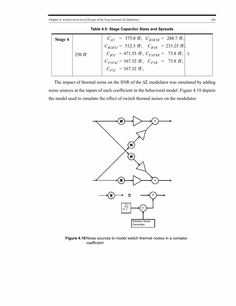
Chapter 4: Architectural-Level Design of the Experimental ΔΣ Modulator 146
The impact of thermal noise on the SNR of the ΔΣ modulator was simulated by adding
noise sources at the inputs of each coefficient in the behavioral model. Figure 4.19 depicts
the model used to simulate the effect of switch thermal noises on the modulator.
Figure 4.19Noise sources to model switch thermal noises in a complex coefficient
+
+
×kTC------
Random NoiseGenerator
+
Stage 4
250 fF
CA3 = 375.0 fF, CB2B3R = 288.7 fF,CB2B3I = 512.3 fF, CB3R = 233.25 fF,CB3I = 471.55 fF, CF3F4R = 73.8 fF,
CF3F4I = 167.32 fF, CF3R = 73.8 fF,CF3I = 167.32 fF,
7
Table 4.5: Stage Capacitor Sizes and Spreads
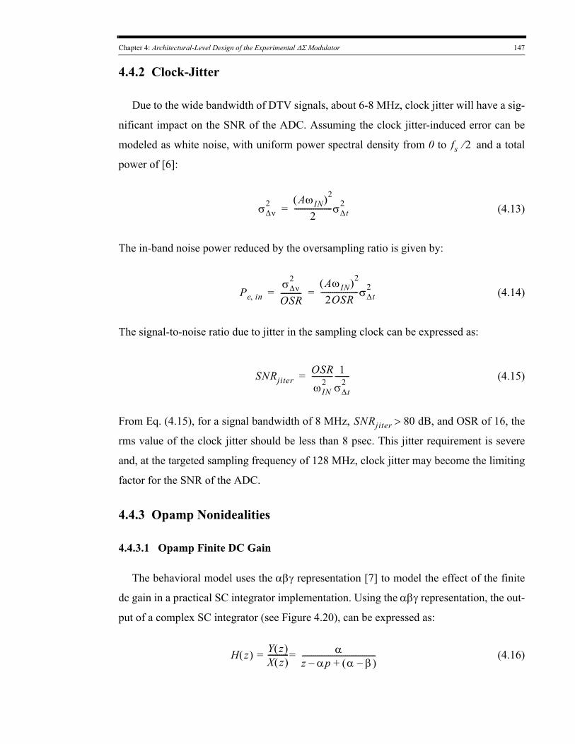
Chapter 4: Architectural-Level Design of the Experimental ΔΣ Modulator 147
4.4.2 Clock-Jitter
Due to the wide bandwidth of DTV signals, about 6-8 MHz, clock jitter will have a sig-
nificant impact on the SNR of the ADC. Assuming the clock jitter-induced error can be
modeled as white noise, with uniform power spectral density from 0 to fs 2⁄ and a total
power of [6]:
σΔν2 AωIN( )2
2--------------------σΔt
2= (4.13)
The in-band noise power reduced by the oversampling ratio is given by:
Pe in,σΔν
2
OSR-----------
AωIN( )2
2OSR--------------------σΔt
2= = (4.14)
The signal-to-noise ratio due to jitter in the sampling clock can be expressed as:
SNRjiterOSRωIN
2----------- 1
σΔt2
--------= (4.15)
From Eq. (4.15), for a signal bandwidth of 8 MHz, SNRjiter 80 > dB, and OSR of 16, the
rms value of the clock jitter should be less than 8 psec. This jitter requirement is severe
and, at the targeted sampling frequency of 128 MHz, clock jitter may become the limiting
factor for the SNR of the ADC.
4.4.3 Opamp Nonidealities
4.4.3.1 Opamp Finite DC Gain
The behavioral model uses the αβγ representation [7] to model the effect of the finite
dc gain in a practical SC integrator implementation. Using the αβγ representation, the out-
put of a complex SC integrator (see Figure 4.20), can be expressed as:
H z( ) Y z( )X z( )----------- α
z αp– α β–( )+---------------------------------------== (4.16)
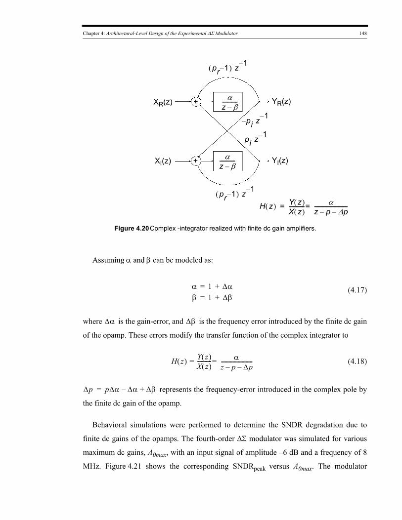
Chapter 4: Architectural-Level Design of the Experimental ΔΣ Modulator 148
αz β–------------
αz β–------------+
+XR(z)
XI(z)
YR(z)
YI(z)
pi z1–
Figure 4.20Complex -integrator realized with finite dc gain amplifiers.
H z( ) Y z( )X z( )------------ α
z p– Δp–-------------------------==
pi– z 1–
pr 1–( ) z 1–
pr 1–( ) z 1–
Assuming α and β can be modeled as:
α = 1 + Δαβ = 1 + Δβ
(4.17)
where Δα is the gain-error, and Δβ is the frequency error introduced by the finite dc gain
of the opamp. These errors modify the transfer function of the complex integrator to
H z( ) Y z( )X z( )----------- α
z p– Δp–------------------------==
Δp pΔα Δα– Δβ+=
(4.18)
represents the frequency-error introduced in the complex pole by
the finite dc gain of the opamp.
Behavioral simulations were performed to determine the SNDR degradation due to
finite dc gains of the opamps. The fourth-order ΔΣ modulator was simulated for various
maximum dc gains, A0max, with an input signal of amplitude –6 dB and a frequency of 8
MHz. Figure 4.21 shows the corresponding SNDRpeak versus A0max. The modulator
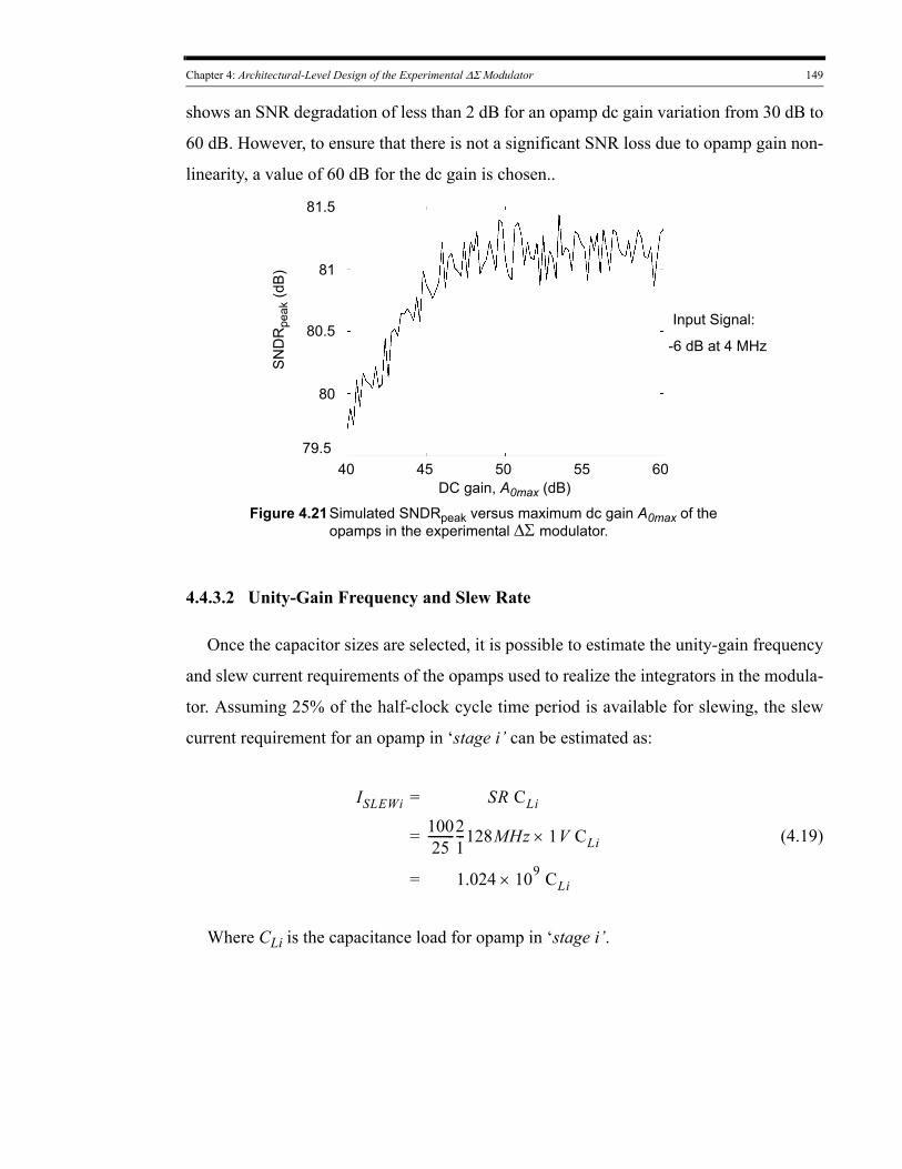
Chapter 4: Architectural-Level Design of the Experimental ΔΣ Modulator 149
shows an SNR degradation of less than 2 dB for an opamp dc gain variation from 30 dB to
60 dB. However, to ensure that there is not a significant SNR loss due to opamp gain non-
linearity, a value of 60 dB for the dc gain is chosen..
Figure 4.21Simulated SNDRpeak versus maximum dc gain A0max of the opamps in the experimental ΔΣ modulator.
Input Signal:
-6 dB at 4 MHz
SN
DR
peak
(dB
)
DC gain, A0max (dB)
79.5
80
80.5
81
81.5
40 45 50 55 60
4.4.3.2 Unity-Gain Frequency and Slew Rate
Once the capacitor sizes are selected, it is possible to estimate the unity-gain frequency
and slew current requirements of the opamps used to realize the integrators in the modula-
tor. Assuming 25% of the half-clock cycle time period is available for slewing, the slew
current requirement for an opamp in ‘stage i’ can be estimated as:
ISLEWi = SR CLi
= 10025---------2
1---128MHz 1V× CLi
= 1.024 109 CLi×
(4.19)
Where CLi is the capacitance load for opamp in ‘stage i’.
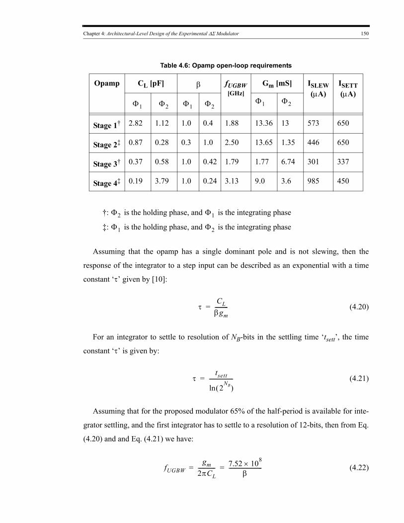
Chapter 4: Architectural-Level Design of the Experimental ΔΣ Modulator 150
Table 4.6: Opamp open-loop requirements
Opamp CL [pF] β fUGBW [GHz]
Gm [mS] ISLEW(μA)
ISETT(μA)
Φ1 Φ2 Φ1 Φ2Φ1 Φ2
Stage 1† 2.82 1.12 1.0 0.4 1.88 13.36 13 573 650
Stage 2‡ 0.87 0.28 0.3 1.0 2.50 13.65 1.35 446 650
Stage 3† 0.37 0.58 1.0 0.42 1.79 1.77 6.74 301 337
Stage 4‡ 0.19 3.79 1.0 0.24 3.13 9.0 3.6 985 450
†: Φ2 is the holding phase, and Φ1 is the integrating phase
‡: Φ1 is the holding phase, and Φ2 is the integrating phase
Assuming that the opamp has a single dominant pole and is not slewing, then the
response of the integrator to a step input can be described as an exponential with a time
constant ‘τ’ given by [10]:
τCL
βgm----------= (4.20)
For an integrator to settle to resolution of NB-bits in the settling time ‘tsett’, the time
constant ‘τ’ is given by:
τtsett
2NB( )ln
------------------= (4.21)
Assuming that for the proposed modulator 65% of the half-period is available for inte-
grator settling, and the first integrator has to settle to a resolution of 12-bits, then from Eq.
(4.20) and and Eq. (4.21) we have:
fUGBWgm
2πCL------------- 7.52 108×
β-------------------------= = (4.22)
Chapter 4: Architectural-Level Design of the Experimental ΔΣ Modulator 151
Eq. (4.22) was used to calculate the unity-gain frequency (fUGBW) requirements for the
four opamps. The calculated values for fUGBW are shown in Table 4.6. However, due to the
noise-shaping in the ΔΣ modulator, it should be possible to relax the settling requirements
and hence required fUGBW for the integrators in the subsequent stages. From Eq. (4.22) the
loop-gain bandwidth (fLGBW fUGBW β×= ) for the opamp is 752 MHz.
The opamp input device current required to realize the transconducatnce (gm) shown in
Table 4.6 can be estimated from:
ISETTgmVov
2---------------= (4.23)
The calculated values for ISETT for an overdrive voltage (Vov) of 0.1 V are shown in Table
4.6.
4.4.4 Switch On-Resistances
In an SC implementation of the modulator, the switches are implemented with NMOS
and PMOS devices. The finite switch-on resistance and other non-ideal behavior of these
devices can degrade the performance of the integrators and of the modulator as a whole.
It is possible to decide on the type of the switch, PMOS, NMOS, or CMOS transmis-
sion gate, on the basis of the node to which the switch is coupled. For example, switches
coupled to the summing junction of the integrator have one side either connected to analog
ground or to the summing junction of the opamp. With the switch arrangement shown in
Figure 4.13, and with the choice of low-voltage for analog ground , it should be possible
to use NMOS devices for the summing junction switches. The switches coupled to the
input signal or the output of the opamp have full signal swing across them and, as a result,
it may be necessary to use CMOS transmission gates for these switches. To minimize par-
asitics, minimum gate length devices will be chosen. The aspect ratio W/L of the devices
Chapter 4: Architectural-Level Design of the Experimental ΔΣ Modulator 152
will also be selected so that the time constant TON RONC( )= of the switch satisfies the
equation [11]:
TONmT7
--------< (4.24)
where mT is the time-period available for the charging of the capacitor C.
Chapter 4: Architectural-Level Design of the Experimental ΔΣ Modulator 153
References[1] Richard Schreier and Gabor C. Temes, Understanding Delta-Sigma Data
Converters. Wiley-IEEE Press, 2004. ISBN 0-471-46585-2.
[2] The Math Works, Inc., Simulink, Version 6.4, Natick, Massachusets: The Math Works, Inc.,
[3] S. A. Jantzi, K. W. Martin, and A. S. Sedra, “The effects of mismatch in complex bandpass ΔΣ modulators,” IEEE International Symposium on Circuits and Systems, vol. 1, 12-15, May 1996, pp. 227-230.
[4] J. G. Kenney and L. R. Carley, ‘‘CLANS: A high-level synthesis tool for high resolution data converters,” ICCAD Dig. Tech Papers, November 1988, pp. 496-499.
[5] D. G. Haigh and B. Singh, ‘‘A switching scheme for switched capacitor filters which reduces the effect of parasitic capacitances associated with switch control terminal,” Proc. IEEE Int. Symp. Circuits Syst., June 1983, vol. 2, pp. 586-589.
[6] B. E. Boser and B. A. Wooley, ‘‘The design of sigma-delta modulation analog-to-digital converters,” IEEE J. Solid-State Circuits, vol. 26, no. 12, pp. 1746-1756, December 1991.
[7] W. -H. Ki and G. C. Temes, ‘‘Offset-compensated switched-capacitor integrators,” Proc. IEEE Int. Symp. Circuits Syst., May 1990, pp. 2829-2832.
[8] R. Schreier, J. Silva, J. Steensgaard and G.C. Temes, ‘‘Design-oriented estimation of thermal noise in switched-capacitor circuits,” IEEE Transactions on Circuits and Systems, vol. 15, no. 11, pp. 2358-2368, November 2005.
[9] Wolfram Research, Inc., Mathematica, Version 6.0, Champaign, IL., Wolfram Research.
[10] Gabor C. Temes, ‘‘Finite amplifier gain and bandwidth effects in switched-capacitor filters,” IEEE J. Solid-State Circuits, vol. 15, no. 3, pp. 358-361, June 1980.
[11] Roubik Gregorian and Gabor C. Temes, Analog MOS Integrated Circuits For Signal Processing. Wiley-Interscience, 1986. ISBN 978-0471097976.
CHAPTER
Integrated Circuit Implementation
The previous chapter discussed the architecture and system level considerations in the
design of the proposed fourth-order complex ΔΣ modulator. The required specifications
for each building block were also discussed in that chapter. This chapter discusses the
implementation of each of these blocks in a 0.18μm CMOS technology. Due to a high
sampling clock frequency and the mixed-signal nature of the ADC, special care has to be
taken to minimize the cross-talk of digital noise into the sensitive analog nodes. In chapter
4, the impact of mismatch on the SNDR and IMR of the ADC was discussed. In the layout
of the ADC, special attention must be paid to minimizing the mismatch between the real
and the quadrature channels. The chapter discusses the layout considerations that were
taken into account and the techniques that were followed during the layout of the proposed
ΔΣ modulator.
5.1 The Complete Fourth-Order SC-Modulator
The discrete nature of the proposed ΔΣ modulator lends itself easily to realization with
switched-capacitor (SC) circuits. Due to the advantages of higher power supply rejection,
reduced clock feed-through and charge injection errors, rejection of even-order non-lin-
earities, and increased dynamic range, a fully-differential configuration was chosen for the
implementation of the SC circuits. The single-ended representation of the SC implementa-
tion of the ΔΣ modulator presented in Chapter 4 is shown again in Figure 5.1.
5
154
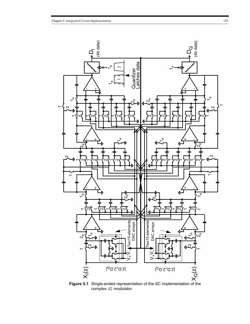
Chapter 5: Integrated Circuit Implementation 155
Figure 5.1 Single-ended representation of the SC implementation of the complex ΔΣ modulator.
X I(z
)
XQ
(z)
DI
DQ
V+V
-1
21 e
1
{2.DI,2.DQ}
2 e-
--
-
-
+
12
21
2 e
211 2 1 1 222 1
1 e
1 e
1
{2.DI,2.DQ}
Qua
ntiz
erLa
tche
s da
ta
2 e
2
2
1 e
1
Two1
5-el
emen
tsD
AC
arra
ys
Two1
5-el
emen
tsD
AC
arra
ys
2 e+
+
+
+
2
1 2 1 2 2 1 2 11 e
1 2 1 2 1
1 2 1 12
1 e
2 1 2 1
2
1-
+
+
--
1
1 e
2 21212122 e
2
2
12 e
2
(4b
data
)
(4b
data
)
1 e
11 e
2 1 2 1 2 1 2 1 2
2 e
1
V+V
-
1
+
1 e2 e
1 e
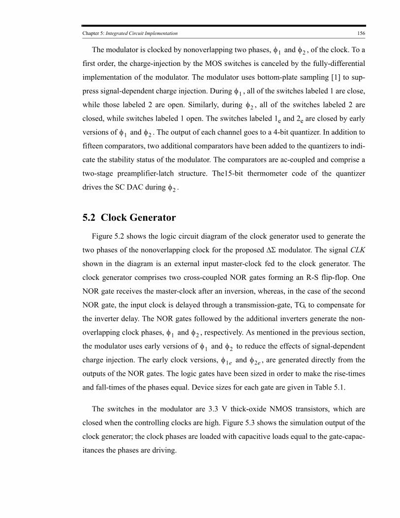
Chapter 5: Integrated Circuit Implementation 156
The modulator is clocked by nonoverlapping two phases, φ1 and φ2 , of the clock. To a
first order, the charge-injection by the MOS switches is canceled by the fully-differential
implementation of the modulator. The modulator uses bottom-plate sampling [1] to sup-
press signal-dependent charge injection. During φ1 , all of the switches labeled 1 are close,
while those labeled 2 are open. Similarly, during φ2 , all of the switches labeled 2 are
closed, while switches labeled 1 open. The switches labeled 1e and 2e are closed by early
versions of φ1 and φ2 . The output of each channel goes to a 4-bit quantizer. In addition to
fifteen comparators, two additional comparators have been added to the quantizers to indi-
cate the stability status of the modulator. The comparators are ac-coupled and comprise a
two-stage preamplifier-latch structure. The15-bit thermometer code of the quantizer
drives the SC DAC during φ2 .
5.2 Clock Generator
Figure 5.2 shows the logic circuit diagram of the clock generator used to generate the
two phases of the nonoverlapping clock for the proposed ΔΣ modulator. The signal CLK
shown in the diagram is an external input master-clock fed to the clock generator. The
clock generator comprises two cross-coupled NOR gates forming an R-S flip-flop. One
NOR gate receives the master-clock after an inversion, whereas, in the case of the second
NOR gate, the input clock is delayed through a transmission-gate, TG, to compensate for
the inverter delay. The NOR gates followed by the additional inverters generate the non-
overlapping clock phases, φ1 and φ2 , respectively. As mentioned in the previous section,
the modulator uses early versions of φ1 and φ2 to reduce the effects of signal-dependent
charge injection. The early clock versions, φ1e and φ2e , are generated directly from the
outputs of the NOR gates. The logic gates have been sized in order to make the rise-times
and fall-times of the phases equal. Device sizes for each gate are given in Table 5.1.
The switches in the modulator are 3.3 V thick-oxide NMOS transistors, which are
closed when the controlling clocks are high. Figure 5.3 shows the simulation output of the
clock generator; the clock phases are loaded with capacitive loads equal to the gate-capac-
itances the phases are driving.
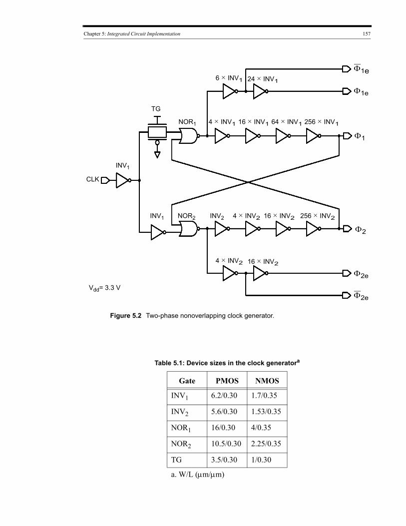
Chapter 5: Integrated Circuit Implementation 157
Figure 5.2 Two-phase nonoverlapping clock generator.
NOR2
NOR1
CLK
TG
Φ2
Φ1
Φ1e
Φ1e
Φ2e
Φ2e
INV2INV1
INV1
4 × INV1 16 × INV1 64 × INV1 256 × INV1
4 × INV2 16 × INV2 256 × INV2
4 × INV2 16 × INV2
6 × INV1 24 × INV1
Vdd= 3.3 V
Table 5.1: Device sizes in the clock generatora
Gate PMOS NMOS
INV1 6.2/0.30 1.7/0.35
INV2 5.6/0.30 1.53/0.35
NOR1 16/0.30 4/0.35
NOR2 10.5/0.30 2.25/0.35
TG 3.5/0.30 1/0.30
a. W/L (μm/μm)
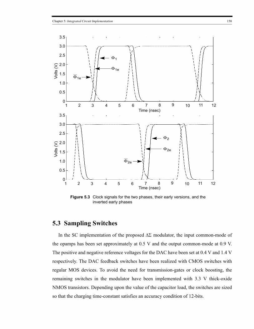
Chapter 5: Integrated Circuit Implementation 158
Figure 5.3 Clock signals for the two phases, their early versions, and the inverted early phases
Φ2
Φ1
Φ1e
Φ1e
Φ2e
Φ2e
1 2 3 4 5 6 7 8 9 10 11 12
1 2 3 4 5 6 7 8 9 10 11 12Time (nsec)
Time (nsec)
0
0.5
1.0
1.5
2.0
2.5
3.0
3.5
Volts
(V)
0
0.5
1.0
1.5
2.0
2.5
3.0
3.5
Volts
(V)
5.3 Sampling Switches
In the SC implementation of the proposed ΔΣ modulator, the input common-mode of
the opamps has been set approximately at 0.5 V and the output common-mode at 0.9 V.
The positive and negative reference voltages for the DAC have been set at 0.4 V and 1.4 V
respectively. The DAC feedback switches have been realized with CMOS switches with
regular MOS devices. To avoid the need for transmission-gates or clock boosting, the
remaining switches in the modulator have been implemented with 3.3 V thick-oxide
NMOS transistors. Depending upon the value of the capacitor load, the switches are sized
so that the charging time-constant satisfies an accuracy condition of 12-bits.
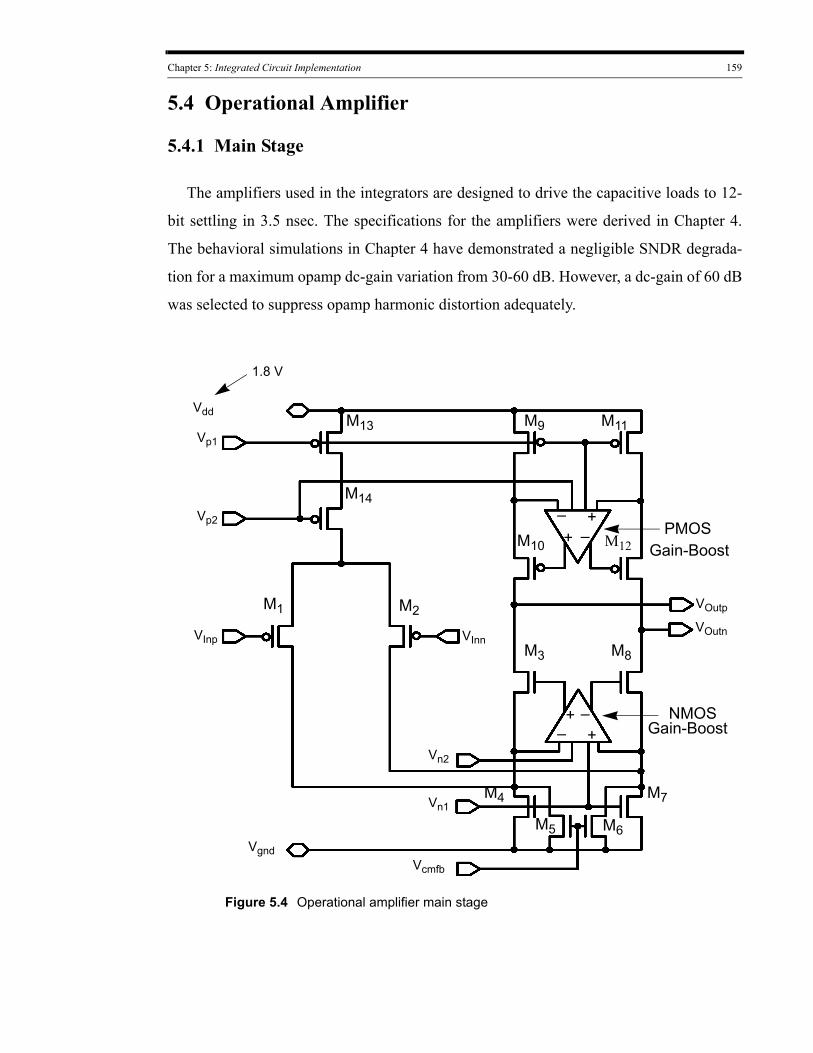
Chapter 5: Integrated Circuit Implementation 159
5.4 Operational Amplifier
5.4.1 Main Stage
The amplifiers used in the integrators are designed to drive the capacitive loads to 12-
bit settling in 3.5 nsec. The specifications for the amplifiers were derived in Chapter 4.
The behavioral simulations in Chapter 4 have demonstrated a negligible SNDR degrada-
tion for a maximum opamp dc-gain variation from 30-60 dB. However, a dc-gain of 60 dB
was selected to suppress opamp harmonic distortion adequately.
Figure 5.4 Operational amplifier main stage
M1 M2
M3 M8
M4 M7
M5 M6
M14
M13 M9 M11
M10 M12PMOS
NMOS
– ++ –
+ –+–
Vp1
Vp2
VInp VInn
VOutp
VOutn
Vcmfb
Vgnd
Vn1
Vn2
Gain-Boost
Gain-Boost
Vdd
1.8 V
Chapter 5: Integrated Circuit Implementation 160
At a power supply of 1.8 V, 60 dB dc-gain can be easily achieved with a single-stage
gain-boosted folded-cascode opamp. The folded-cascode opamp shown in Figure 5.4 is
designed with a PMOS differential pair, M1 and M2. The swing at the output of the opamp
has been maximized by biasing the NMOS current sinks, M3 and M4, and M6 and M8, and
the PMOS current sources, M9 and M10, and M11 and M12, at the edge of the triode region;
the drain-source voltage for these transistors has been set approximately at their overdrive
voltage. For a power supply of 1.8 V, the differential output swing of the opamp is 2 Vp-p.
The output common-mode voltage of the opamp has been set at 0.9 V, which is about half
the supply voltage. The input common-mode of the opamp has been set at approximately
0.5 V, which is a value higher than 0 V, in order to guarantee a minimum positive input
common mode voltage under all conditions [2][3].
Voltages Vp1, Vp2, Vn1, and Vn2 are set by a separate bias stage, and the voltage Vcmfb is
set by the common-mode feedback voltage circuit. The NMOS cascode transistors, M3
and M6, and the PMOS cascode transistors, M10 and M12, are gain-boosted with additional
fully-differential amplifiers.
The input stage transistors are designed to achieve the desired unity-gain frequency.
The NMOS transistors, M3 and M6, and the PMOS transistors, M10 and M12, have been
designed with minimal lengths (L 0.18μm= ) in order to place the nondominant pole of
the opamp at a high frequency. For transistors M9, M11, M4, M5, M7, and M8 longer chan-
nel lengths have been chosen in order to achieve better matching.
Figure 5.5 shows the closed loop frequency-response simulations of the overall ampli-
fier for the firststage of the modulator. The amplifier achieves a loop-gain of 56 dB, a
loop-gain bandwidth of 750 MHz, and a phase margin greater than 75°.
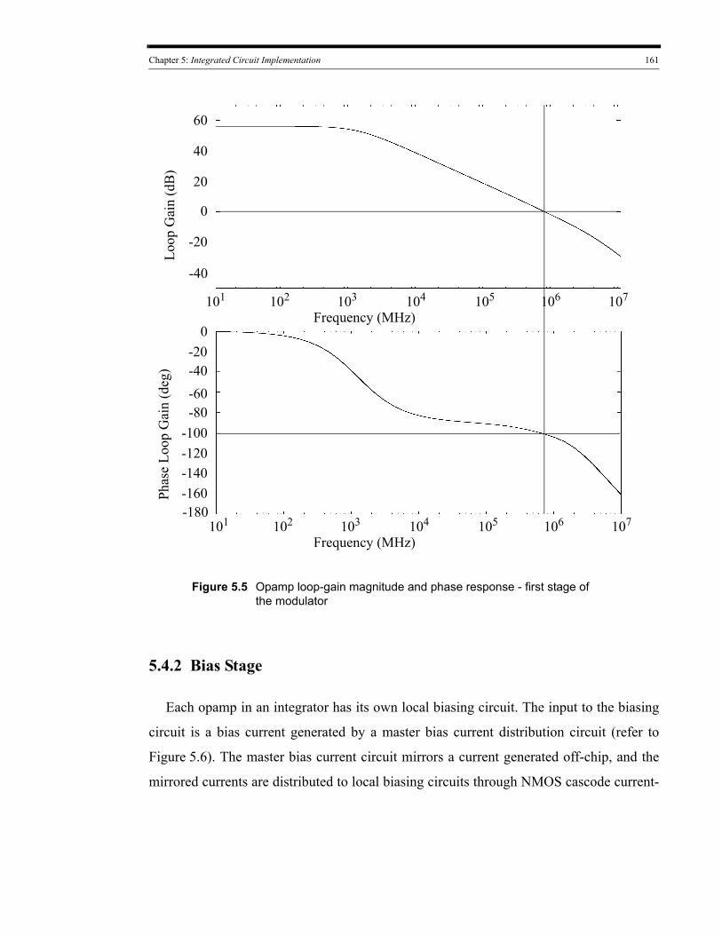
Chapter 5: Integrated Circuit Implementation 161
-40
-20
0
20
40
60
Loop
Gai
n (d
B)
Phas
e Lo
op G
ain
(deg
)
-160-140-120-100-80
0
-180
-60-40-20
Frequency (MHz)101 102 103 104 105 106 107
Frequency (MHz)101 102 103 104 105 106 107
Figure 5.5 Opamp loop-gain magnitude and phase response - first stage of the modulator
5.4.2 Bias Stage
Each opamp in an integrator has its own local biasing circuit. The input to the biasing
circuit is a bias current generated by a master bias current distribution circuit (refer to
Figure 5.6). The master bias current circuit mirrors a current generated off-chip, and the
mirrored currents are distributed to local biasing circuits through NMOS cascode current-
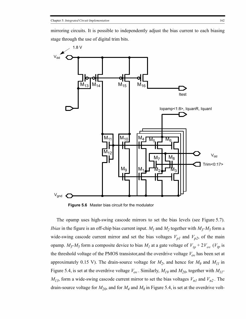
Chapter 5: Integrated Circuit Implementation 162
mirroring circuits. It is possible to independently adjust the bias current to each biasing
stage through the use of digital trim bits.
Figure 5.6 Master bias circuit for the modulator
M13 M16
Vgnd
Vdd
1.8 V
M14 M15
Iopamp<1:8>, IquanR, IquanI
Itest
Vdd
Trim<0:17>
M11 M10
M9
M4 M5 M6
M1 M2 M3
M7 M8
M12
The opamp uses high-swing cascode mirrors to set the bias levels (see Figure 5.7).
Ibias in the figure is an off-chip bias current input. M1 and M2 together with M3-M5 form a
wide-swing cascode current mirror and set the bias voltages Vp1 and Vp2, of the main
opamp. M3-M5 form a composite device to bias M1 at a gate voltage of Vtp 2Vov+ (Vtp is
the threshold voltage of the PMOS transistor,and the overdrive voltage Vov has been set at
approximately 0.15 V). The drain-source voltage for M2, and hence for M9 and M11 in
Figure 5.4, is set at the overdrive voltage Vov . Similarly, M19 and M20, together with M11-
M13, form a wide-swing cascode current mirror to set the bias voltages Vn1 and Vn2 . The
drain-source voltage for M20, and for M4 and M8 in Figure 5.4, is set at the overdrive volt-
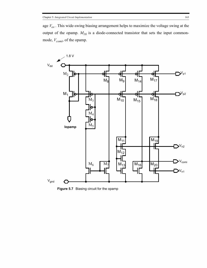
Chapter 5: Integrated Circuit Implementation 163
age Vov . This wide-swing biasing arrangement helps to maximize the voltage swing at the
output of the opamp. M16 is a diode-connected transistor that sets the input common-
mode, Vcomi, of the opamp.
M1M15
M14M8 M9
M2 Vp1
Vp2
Vgnd
Vn1
Vn2
Vcomi
Figure 5.7 Biasing circuit for the opamp
M3
M4
M5
M6 M7
M10
M11
M12
M13 M16
M17
M18
M19
M20
Vdd
1.8 V
Iopamp
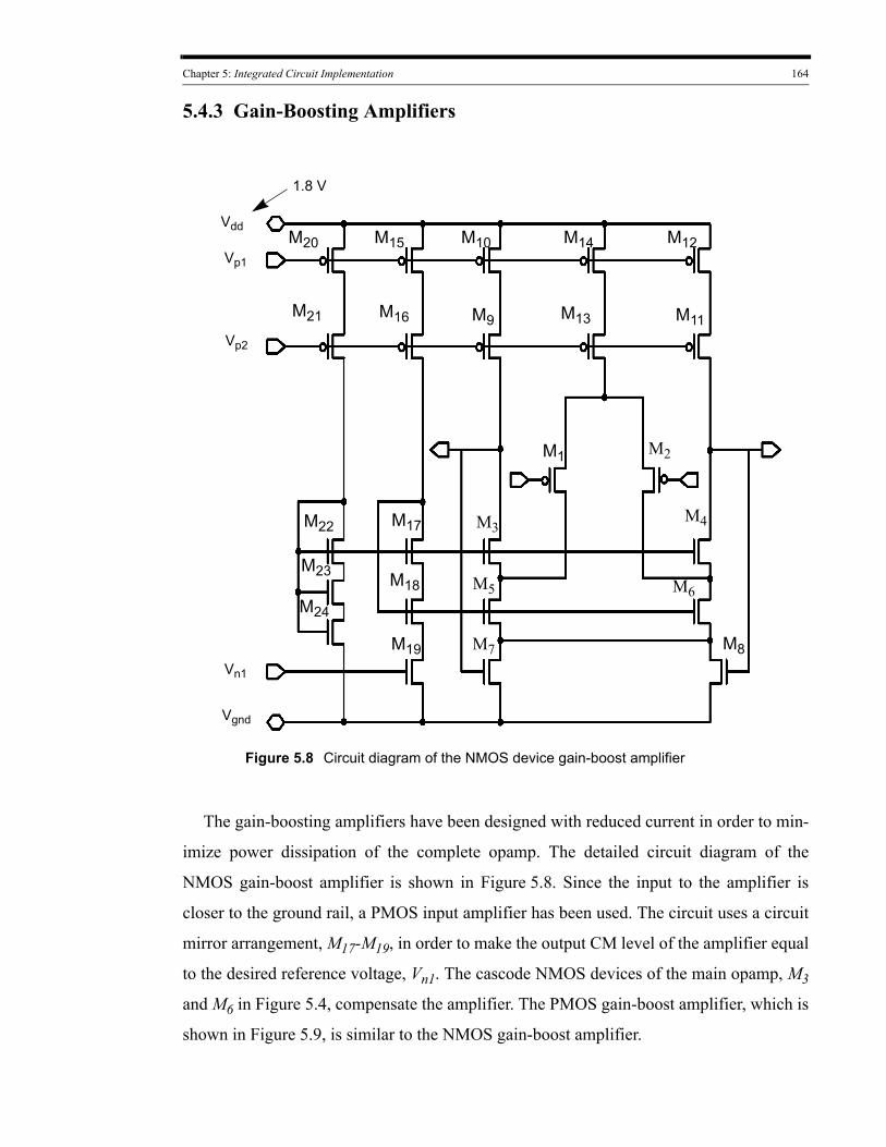
Chapter 5: Integrated Circuit Implementation 164
5.4.3 Gain-Boosting Amplifiers
Figure 5.8 Circuit diagram of the NMOS device gain-boost amplifier
M1
M15 M14
M8
M9
M2
Vp1
Vp2
Vgnd
Vn1
M3M4
M5 M6
M7
M10
M11
M12
M13M16
M17
M19
M20
M18
M21
M22
M23
M24
Vdd
1.8 V
The gain-boosting amplifiers have been designed with reduced current in order to min-
imize power dissipation of the complete opamp. The detailed circuit diagram of the
NMOS gain-boost amplifier is shown in Figure 5.8. Since the input to the amplifier is
closer to the ground rail, a PMOS input amplifier has been used. The circuit uses a circuit
mirror arrangement, M17-M19, in order to make the output CM level of the amplifier equal
to the desired reference voltage, Vn1. The cascode NMOS devices of the main opamp, M3
and M6 in Figure 5.4, compensate the amplifier. The PMOS gain-boost amplifier, which is
shown in Figure 5.9, is similar to the NMOS gain-boost amplifier.
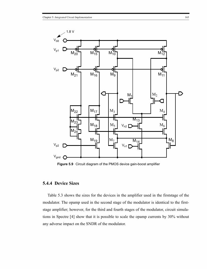
Chapter 5: Integrated Circuit Implementation 165
Figure 5.9 Circuit diagram of the PMOS device gain-boost amplifier
M1
M15
M14 M8
M9
M2
Vp1
Vp2
Vgnd
Vp2
M3 M4
M5 M6
M7
M10
M11
M12
M13
M16
M17
M19
M20
M18
M21
M22
M23
M24
Vn2
Vn1
Vdd
1.8 V
5.4.4 Device Sizes
Table 5.3 shows the sizes for the devices in the amplifier used in the firststage of the
modulator. The opamp used in the second stage of the modulator is identical to the first-
stage amplifier; however, for the third and fourth stages of the modulator, circuit simula-
tions in Spectre [4] show that it is possible to scale the opamp currents by 30% without
any adverse impact on the SNDR of the modulator.
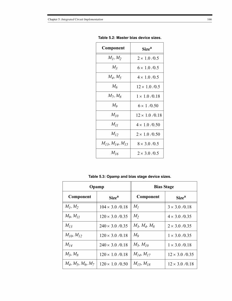
Chapter 5: Integrated Circuit Implementation 166
Table 5.2: Master bias device sizes.
Component Sizea
M1, M2 2 1.0 0.5⁄×
M3 6 1.0 0.5⁄×
M4, M5 4 1.0 0.5⁄×
M6 12 1.0 0.5⁄×
M7, M8 1 1.0 0.18⁄×
M9 6 1 0.50⁄×
M10 12 1.0 0.18⁄×
M11 4 1.0 0.50⁄×
M12 2 1.0 0.50⁄×
M13, M14, M15 8 3.0 0.5⁄×
M16 2 3.0 0.5⁄×
Table 5.3: Opamp and bias stage device sizes.
Opamp Bias Stage
Component Sizea Component Sizea
M1, M2 104 3.0 0.18⁄× M1 3 3.0 0.18⁄×
M9, M11 120 3.0 0.35⁄× M2 4 3.0 0.35⁄×
M13 240 3.0 0.35⁄× M3, M4, M8 2 3.0 0.35⁄×
M10, M12 120 3.0 0.18⁄× M9 1 3.0 0.35⁄×
M14 240 3.0 0.18⁄× M5, M10 1 3.0 0.18⁄×
M3, M8 120 1.0 0.18⁄× M14, M17 12 3.0 0.35⁄×
M4, M5, M6, M7 120 1.0 0.50⁄× M15, M18 12 3.0 0.18⁄×
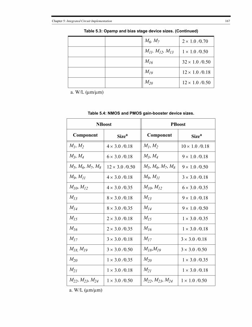
Chapter 5: Integrated Circuit Implementation 167
M6, M7 2 1.0 0.70⁄×
M11, M12, M13 1 1.0 0.50⁄×
M16 32 1.0 0.50⁄×
M19 12 1.0 0.18⁄×
M20 12 1.0 0.50⁄×
a. W/L (μm/μm)
Table 5.4: NMOS and PMOS gain-booster device sizes.
NBoost PBoost
Component Sizea Component Sizea
M1, M2 4 3.0 0.18⁄× M1, M2 10 1.0 0.18⁄×
M3, M4 6 3.0 0.18⁄× M3, M4 9 1.0 0.18⁄×
M5, M6, M7, M8 12 3.0 0.50⁄× M5, M6, M7, M8 9 1.0 0.50⁄×
M9, M11 4 3.0 0.18⁄× M9, M11 3 3.0 0.18⁄×
M10, M12 4 3.0 0.35⁄× M10, M12 6 3.0 0.35⁄×
M13 8 3.0 0.18⁄× M13 9 1.0 0.18⁄×
M14 8 3.0 0.35⁄× M14 9 1.0 0.50⁄×
M15 2 3.0 0.18⁄× M15 1 3.0 0.35⁄×
M16 2 3.0 0.35⁄× M16 1 3.0 0.18⁄×
M17 3 3.0 0.18⁄× M17 3 3.0 0.18⁄×
M18, M19 3 3.0 0.50⁄× M18,M19 3 3.0 0.50⁄×
M20 1 3.0 0.35⁄× M20 1 3.0 0.35⁄×
M21 1 3.0 0.18⁄× M21 1 3.0 0.18⁄×
M22, M23, M24 1 3.0 0.50⁄× M22, M23, M24 1 1.0 0.50⁄×
a. W/L (μm/μm)
Table 5.3: Opamp and bias stage device sizes. (Continued)
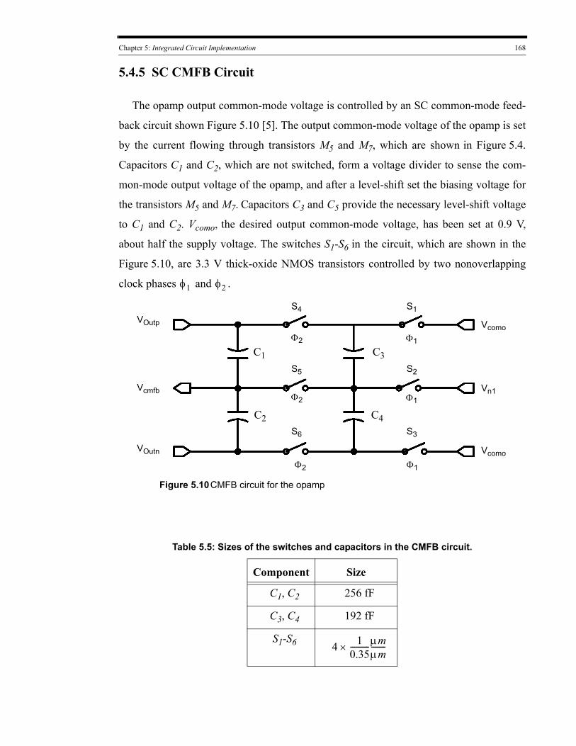
Chapter 5: Integrated Circuit Implementation 168
5.4.5 SC CMFB Circuit
The opamp output common-mode voltage is controlled by an SC common-mode feed-
back circuit shown Figure 5.10 [5]. The output common-mode voltage of the opamp is set
by the current flowing through transistors M5 and M7, which are shown in Figure 5.4.
Capacitors C1 and C2, which are not switched, form a voltage divider to sense the com-
mon-mode output voltage of the opamp, and after a level-shift set the biasing voltage for
the transistors M5 and M7. Capacitors C3 and C5 provide the necessary level-shift voltage
to C1 and C2. Vcomo, the desired output common-mode voltage, has been set at 0.9 V,
about half the supply voltage. The switches S1-S6 in the circuit, which are shown in the
Figure 5.10, are 3.3 V thick-oxide NMOS transistors controlled by two nonoverlapping
clock phases φ1 and φ2 .
Vn1
Vcomo
Vcomo
S4 S1
S2
S3
S5
S6
C3
C4
C1
C2
VOutn
VOutp
Vcmfb
Figure 5.10CMFB circuit for the opamp
Φ1
Φ1
Φ1
Φ2
Φ2
Φ2
Table 5.5: Sizes of the switches and capacitors in the CMFB circuit.
Component Size
C1, C2 256 fF
C3, C4 192 fF
S1-S6 4 10.35----------μm
μm--------×
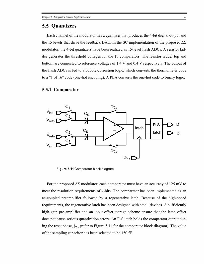
Chapter 5: Integrated Circuit Implementation 169
5.5 Quantizers
Each channel of the modulator has a quantizer that produces the 4-bit digital output and
the 15 levels that drive the feedback DAC. In the SC implementation of the proposed ΔΣ
modulator, the 4-bit quantizers have been realized as 15-level flash ADCs. A resistor lad-
der generates the threshold voltages for the 15 comparators. The resistor ladder top and
bottom are connected to reference voltages of 1.4 V and 0.4 V respectively. The output of
the flash ADCs is fed to a bubble-correction logic, which converts the thermometer code
to a “1 of 16” code (one-hot encoding). A PLA converts the one-hot code to binary logic.
5.5.1 Comparator
Figure 5.11 Comparator block diagram
R-S
latch
D
Dlatch
–
–+
+
Vinp
Vrefp
Vinn
Vrefn
CS
CS
Φ1
Φ2
Φ1
Φ2
Φ2e
Φ2e
Φ1e
For the proposed ΔΣ modulator, each comparator must have an accuracy of 125 mV to
meet the resolution requirements of 4-bits. The comparator has been implemented as an
ac-coupled preamplifier followed by a regenerative latch. Because of the high-speed
requirements, the regenerative latch has been designed with small devices. A sufficiently
high-gain pre-amplifier and an input-offset storage scheme ensure that the latch offset
does not cause serious quantization errors. An R-S latch holds the comparator output dur-
ing the reset phase, φ2e (refer to Figure 5.11 for the comparator block diagram). The value
of the sampling capacitor has been selected to be 150 fF.
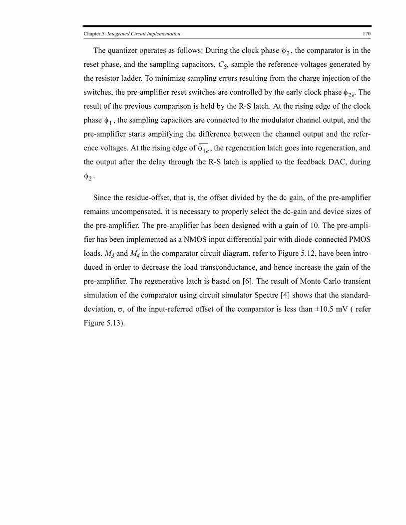
Chapter 5: Integrated Circuit Implementation 170
The quantizer operates as follows: During the clock phase φ2 , the comparator is in the
reset phase, and the sampling capacitors, CS, sample the reference voltages generated by
the resistor ladder. To minimize sampling errors resulting from the charge injection of the
switches, the pre-amplifier reset switches are controlled by the early clock phase φ2e. The
result of the previous comparison is held by the R-S latch. At the rising edge of the clock
phase φ1 , the sampling capacitors are connected to the modulator channel output, and the
pre-amplifier starts amplifying the difference between the channel output and the refer-
ence voltages. At the rising edge of φ1e , the regeneration latch goes into regeneration, and
the output after the delay through the R-S latch is applied to the feedback DAC, during
φ2 .
Since the residue-offset, that is, the offset divided by the dc gain, of the pre-amplifier
remains uncompensated, it is necessary to properly select the dc-gain and device sizes of
the pre-amplifier. The pre-amplifier has been designed with a gain of 10. The pre-ampli-
fier has been implemented as a NMOS input differential pair with diode-connected PMOS
loads. M3 and M4 in the comparator circuit diagram, refer to Figure 5.12, have been intro-
duced in order to decrease the load transconductance, and hence increase the gain of the
pre-amplifier. The regenerative latch is based on [6]. The result of Monte Carlo transient
simulation of the comparator using circuit simulator Spectre [4] shows that the standard-
deviation, σ, of the input-referred offset of the comparator is less than ±10.5 mV ( refer
Figure 5.13).
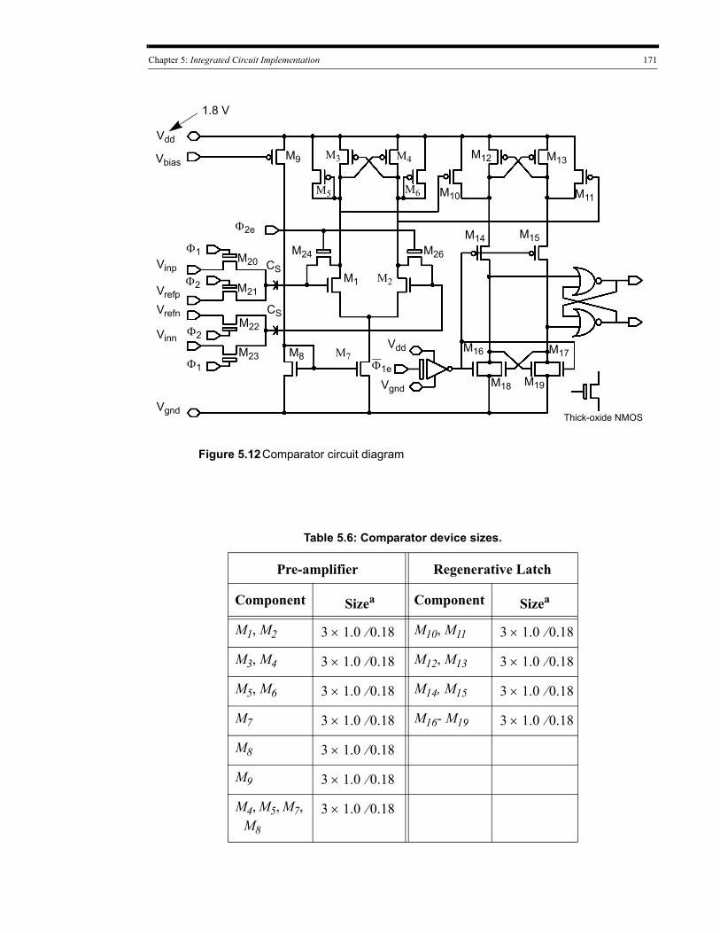
Chapter 5: Integrated Circuit Implementation 171
M1
M15M14
M8
M9
M2
Vgnd
Vdd
M3 M4
M5 M6
M7
M10 M11
M12 M13
M16 M17
M19
M20
M18
M21
M22
M23
M24Vinp
Vrefp
Vrefn
Vinn
M26
Φ2
Φ2
Φ1
Φ1 Φ1e
1.8 V
Figure 5.12Comparator circuit diagram
Thick-oxide NMOS
CS
CS
Vbias
Φ2e
Vdd
Vgnd
Table 5.6: Comparator device sizes.
Pre-amplifier Regenerative Latch
Component Sizea Component Sizea
M1, M2 3 1.0 0.18⁄× M10, M11 3 1.0 0.18⁄×
M3, M4 3 1.0 0.18⁄× M12, M13 3 1.0 0.18⁄×
M5, M6 3 1.0 0.18⁄× M14, M15 3 1.0 0.18⁄×
M7 3 1.0 0.18⁄× M16- M19 3 1.0 0.18⁄×
M8 3 1.0 0.18⁄×
M9 3 1.0 0.18⁄×
M4, M5, M7, M8
3 1.0 0.18⁄×
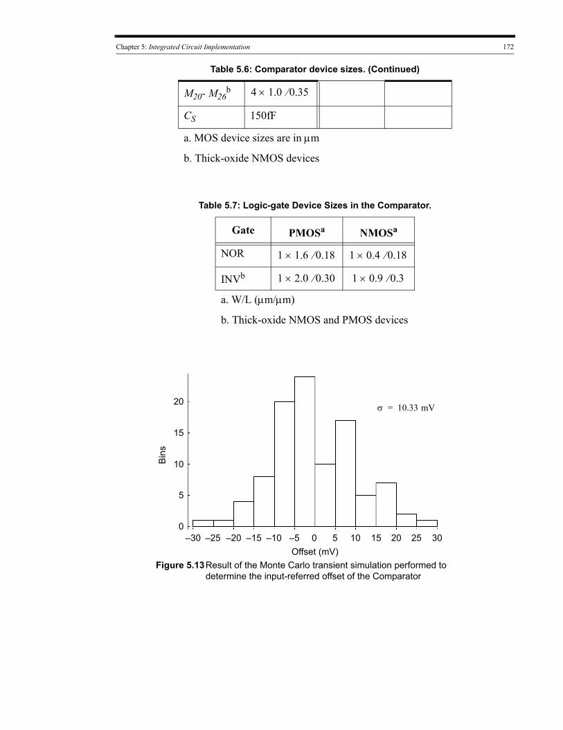
Chapter 5: Integrated Circuit Implementation 172
M20- M26b 4 1.0 0.35⁄×
CS 150fF
a. MOS device sizes are in μm
b. Thick-oxide NMOS devices
Table 5.7: Logic-gate Device Sizes in the Comparator.
Gate PMOSa NMOSa
NOR 1 1.6 0.18⁄× 1 0.4 0.18⁄×
INVb 1 2.0 0.30⁄× 1 0.9 0.3⁄×
a. W/L (μm/μm)
b. Thick-oxide NMOS and PMOS devices
Figure 5.13Result of the Monte Carlo transient simulation performed to determine the input-referred offset of the Comparator
–30 –25 –20 –15 –10 –5 0 5 10 15 20 25 300
5
10
15
20σ 10.33 mV=
Bin
s
Offset (mV)
Table 5.6: Comparator device sizes. (Continued)
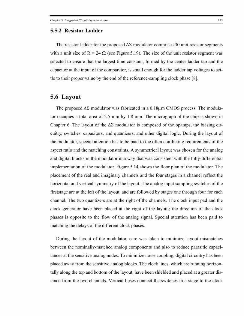
Chapter 5: Integrated Circuit Implementation 173
5.5.2 Resistor Ladder
The resistor ladder for the proposed ΔΣ modulator comprises 30 unit resistor segments
with a unit size of R = 24 Ω (see Figure 5.19). The size of the unit resistor segment was
selected to ensure that the largest time constant, formed by the center ladder tap and the
capacitor at the input of the comparator, is small enough for the ladder tap voltages to set-
tle to their proper value by the end of the reference-sampling clock phase [8].
5.6 Layout
The proposed ΔΣ modulator was fabricated in a 0.18μm CMOS process. The modula-
tor occupies a total area of 2.5 mm by 1.8 mm. The micrograph of the chip is shown in
Chapter 6. The layout of the ΔΣ modulator is composed of the opamps, the biasing cir-
cuitry, switches, capacitors, and quantizers, and other digital logic. During the layout of
the modulator, special attention has to be paid to the often conflicting requirements of the
aspect ratio and the matching constraints. A symmetrical layout was chosen for the analog
and digital blocks in the modulator in a way that was consistent with the fully-differential
implementation of the modulator. Figure 5.14 shows the floor plan of the modulator. The
placement of the real and imaginary channels and the four stages in a channel reflect the
horizontal and vertical symmetry of the layout. The analog input sampling switches of the
firststage are at the left of the layout, and are followed by stages one through four for each
channel. The two quantizers are at the right of the channels. The clock input pad and the
clock generator have been placed at the right of the layout; the direction of the clock
phases is opposite to the flow of the analog signal. Special attention has been paid to
matching the delays of the different clock phases.
During the layout of the modulator, care was taken to minimize layout mismatches
between the nominally-matched analog components and also to reduce parasitic capaci-
tances at the sensitive analog nodes. To minimize noise coupling, digital circuitry has been
placed away from the sensitive analog blocks. The clock lines, which are running horizon-
tally along the top and bottom of the layout, have been shielded and placed at a greater dis-
tance from the two channels. Vertical buses connect the switches in a stage to the clock
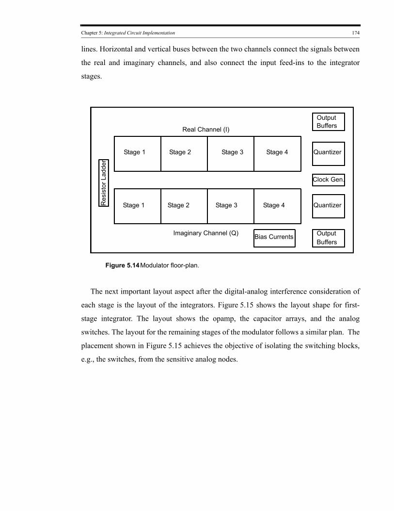
Chapter 5: Integrated Circuit Implementation 174
lines. Horizontal and vertical buses between the two channels connect the signals between
the real and imaginary channels, and also connect the input feed-ins to the integrator
stages.
Figure 5.14Modulator floor-plan.
Real Channel (I)
Imaginary Channel (Q)
Stage 1
Stage 1
Stage 2 Stage 3 Stage 4
Stage 2 Stage 3 Stage 4Res
isto
r Lad
der
Quantizer
Quantizer
Clock Gen.
Output Buffers
Output Buffers
Bias Currents
The next important layout aspect after the digital-analog interference consideration of
each stage is the layout of the integrators. Figure 5.15 shows the layout shape for first-
stage integrator. The layout shows the opamp, the capacitor arrays, and the analog
switches. The layout for the remaining stages of the modulator follows a similar plan. The
placement shown in Figure 5.15 achieves the objective of isolating the switching blocks,
e.g., the switches, from the sensitive analog nodes.
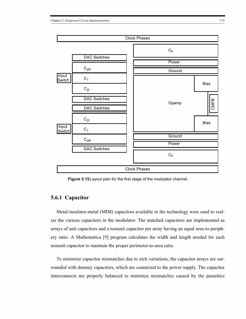
Chapter 5: Integrated Circuit Implementation 175
Figure 5.15Layout plan for the first stage of the modulator channel.
Clock Phases
Power
Ground
CF
DAC Switches
C2R
C1
C2I
DAC Switches
DAC Switches
C2I
C1
C2R
DAC Switches
Opamp
Clock Phases
Input
InputSwitch
Switch
CM
FB
Ground
Power
CF
Bias
Bias
5.6.1 Capacitor
Metal-insulator-metal (MIM) capacitors available in the technology were used to real-
ize the various capacitors in the modulator. The matched capacitors are implemented as
arrays of unit capacitors and a nonunit capacitor per array having an equal area-to-periph-
ery ratio. A Mathematica [9] program calculates the width and length needed for each
nonunit capacitor to maintain the proper perimeter-to-area ratio.
To minimize capacitor mismatches due to etch variations, the capacitor arrays are sur-
rounded with dummy capacitors, which are connected to the power supply. The capacitor
interconnects are properly balanced to minimize mismatches caused by the parasitics
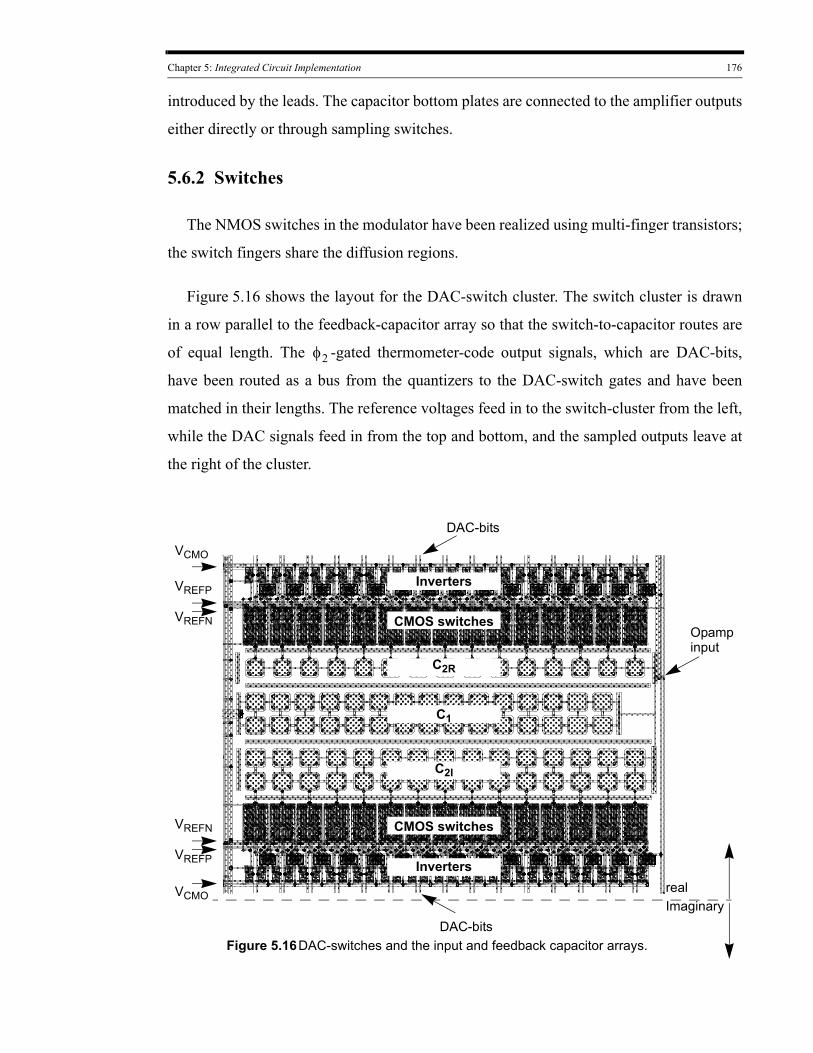
Chapter 5: Integrated Circuit Implementation 176
introduced by the leads. The capacitor bottom plates are connected to the amplifier outputs
either directly or through sampling switches.
5.6.2 Switches
The NMOS switches in the modulator have been realized using multi-finger transistors;
the switch fingers share the diffusion regions.
Figure 5.16 shows the layout for the DAC-switch cluster. The switch cluster is drawn
in a row parallel to the feedback-capacitor array so that the switch-to-capacitor routes are
of equal length. The φ2 -gated thermometer-code output signals, which are DAC-bits,
have been routed as a bus from the quantizers to the DAC-switch gates and have been
matched in their lengths. The reference voltages feed in to the switch-cluster from the left,
while the DAC signals feed in from the top and bottom, and the sampled outputs leave at
the right of the cluster.
C2R
C1
C2I
CMOS switches
Inverters
CMOS switches
Inverters
Figure 5.16DAC-switches and the input and feedback capacitor arrays.
DAC-bits
realImaginary
DAC-bits
VREFP
VREFNOpampinput
VCMO
VREFN
VREFP
VCMO
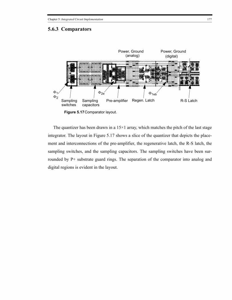
Chapter 5: Integrated Circuit Implementation 177
5.6.3 Comparators
Sampling switches
Sampling Pre-amplifier Regen. Latch
(analog) Power, Ground
(digital) Power, Ground
Φ1,
R-S Latch
Figure 5.17Comparator layout.
Φ2
Φ2e Φ1eb
capacitors
The quantizer has been drawn in a 15×1 array, which matches the pitch of the last stage
integrator. The layout in Figure 5.17 shows a slice of the quantizer that depicts the place-
ment and interconnections of the pre-amplifier, the regenerative latch, the R-S latch, the
sampling switches, and the sampling capacitors. The sampling switches have been sur-
rounded by P+ substrate guard rings. The separation of the comparator into analog and
digital regions is evident in the layout.
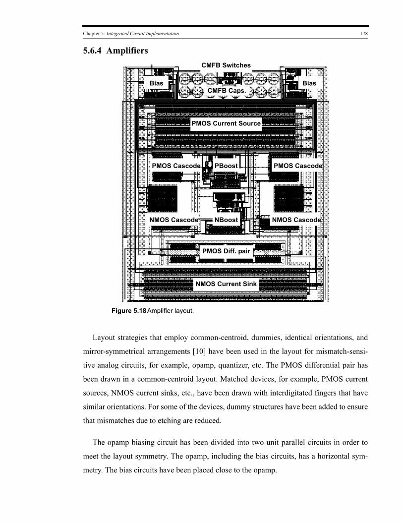
Chapter 5: Integrated Circuit Implementation 178
5.6.4 AmplifiersCMFB Switches
Bias Bias
PMOS Current Source
PBoost
NBoost
NMOS Current Sink
PMOS Diff. pair
PMOS Cascode PMOS Cascode
NMOS CascodeNMOS Cascode
CMFB Caps.
Figure 5.18Amplifier layout.
Layout strategies that employ common-centroid, dummies, identical orientations, and
mirror-symmetrical arrangements [10] have been used in the layout for mismatch-sensi-
tive analog circuits, for example, opamp, quantizer, etc. The PMOS differential pair has
been drawn in a common-centroid layout. Matched devices, for example, PMOS current
sources, NMOS current sinks, etc., have been drawn with interdigitated fingers that have
similar orientations. For some of the devices, dummy structures have been added to ensure
that mismatches due to etching are reduced.
The opamp biasing circuit has been divided into two unit parallel circuits in order to
meet the layout symmetry. The opamp, including the bias circuits, has a horizontal sym-
metry. The bias circuits have been placed close to the opamp.
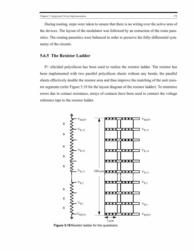
Chapter 5: Integrated Circuit Implementation 179
During routing, steps were taken to ensure that there is no wiring over the active area of
the devices. The layout of the modulator was followed by an extraction of the route para-
sitics. The routing parasitics were balanced in order to preserve the fully-differential sym-
metry of the circuits.
5.6.5 The Resistor Ladder
P+ silicided polysilicon has been used to realize the resistor ladder. The resistor has
been implemented with two parallel polysilicon sheets without any bends; the parallel
sheets effectively double the resistor area and thus improve the matching of the unit resis-
tor segments (refer Figure 5.19 for the layout diagram of the resistor ladder). To minimize
errors due to contact resistance, arrays of contacts have been used to connect the voltage
reference taps to the resistor ladder.
VREFP
VR,15
VR,14
VR,2
VREFN
VR,1
R
R
R
R
R
R
R
R
VREFP
VR,15
VR,14
VR,13
VR,2
VREFN
VR,1
Figure 5.19Resistor ladder for the quantizers.
280 μm
3 μm
VR,13
Chapter 5: Integrated Circuit Implementation 180
5.7 Substrate and Supply Noise Decoupling
The chip has been partitioned into analog and digital regions, and separate power sup-
plies power the analog and digital circuits. The power supplies have been connected
through separate bonding pads to off-chip voltage regulators. Well and substrate contacts
have been used to improve the isolation between the analog and the digital circuits. To
reduce the threshold-voltage modulation of the NMOS analog devices caused by body
effect, the NMOS devices have been surrounded with a p+ substrate ring, which is con-
nected to the local analog ground.
P+ substrate ties, which are biased to ground, and N-well guard rings, which are biased
at power supply, have been placed between the sensitive analog circuits, e.g., the opamps,
and between the analog and digital regions to improve the isolation between the circuits1.
Multiple substrate contacts biased to analog ground have been placed close to sensitive
analog nodes and in the unused chip area. On-chip decoupling capacitors formed of
PMOS devices have been placed under the power buses and other unused chip area in
order to reduce the high-frequency noise on the power supplies.
Metal-layer shielding has been used to protect signal paths and to isolate sensitive ana-
log nodes, e.g., opamp inputs, from the noisy signals. A separate pad powers the metal-
layer shield from an off-chip supply. Clocks have been distributed through buses. The
clock buses have been shielded by a digital power supply in order to reduce clock noise
injection through bus parasitics into the substrate, and hence into the analog ground.
The selected CMOS technology offers deep N-well, an optional layer for isolating the
noise from the P-substrate. To minimize noise injection of the switching digital bits into
the substrate, the I/O drivers have been realized in an isolated P-substrate, which was cre-
ated by surrounding deep N-well with N-well guard ring. The power and ground for the I/
O drivers have been routed from separate bonding pads.
1. Due to the low-ohmic substrate of the selected CMOS technology, guard rings are not expected to attenuate substrate coupling significantly.
Chapter 5: Integrated Circuit Implementation 181
References[1] D. G. Haigh and B. Singh, ‘‘A switching scheme for switched capacitor filters
which reduces the effect of parasitic capacitances associated with switch control terminal,” Proc. IEEE Int. Symp. Circuits Syst., June 1983, vol. 2, pp. 586-589.
[2] Mohammed Dessouky, and Andreas Kaiser, ‘‘Very low-voltage digital-audio DS modulator with 88-dB dynamic range using local switch bootstrapping,’’ IEEE J. Solid-State Circuits, vol.36, no. 3, pp. 349-355, March 2001.
[3] A. Baschirotto, and R. Castello, “A 1-V 1.8-MHz CMOS switched-opamp SC filter with rail-to-rail output swing,” IEEE J.Solid-State Circuits, vol. 32, no. 12, pp. 1979–1986, December 1997.
[4] Cadence Design Systems Inc., Spectre, Version 6.1.1, San Jose, California.
[5] D. Senderowicz, S. F. Dreyer, J. H. Huggins, and C. A. Laber, “A family of differential NMOS analog circuits for a PCM codec filter chip,” IEEE J.Solid-State Circuits, vol. 17, no. 6, pp. 1014–1023, December 1982.
[6] Akira Yukawa, ‘‘A CMOS 8-bit high-speed A/D converter IC,’’ IEEE J. Solid-State Circuits, vol. SC-20, no. 3, pp. 775-779, June 1985.
[7] D. Senderowicz, S. F. Dreyer, J. H. Huggins, C. F. Rahim, and C. A. Laber, “A family of differential NMOS analog circuits for a PCM codec filter chip,” IEEE J.Solid-State Circuits, vol. 17, no. 6, pp. 1014–1023, December 1982.
[8] M. Rebeschini, and P.F. Ferguson, ‘‘Analog circuit design for DS DACs,” in Delta-Sigma Data Converters: Theory, Design, and Simulation, S. R. Norsworthy, R. Schreier, and G. C. Temes, Eds. New York: IEEE Press, 1997, ch. 12.
[9] Wolfram Research, Inc., Mathematica, Version 6.0, Champaign, IL., Wolfram Research.
[10] A. Hastings, The Art of Analog Layout (2nd Edition), ISBN 0131464108, Prentice Hall, New Jersey, 2005.
CHAPTER
Testing and Experimental Results
This chapter discusses the testing and experimental results of the proposed fourth-order
complex ΔΣ modulator. Some other system considerations that emerged during the design
of the test set-up for the modulator, for example, the PCB layout and chip biasing, are also
discussed in this chapter. Finally, the experimental results, which are based on the data
captured using the test set-up, are presented in the chapter.
6.1 The Integrated Circuit
The proposed ΔΣ modulator was fabricated in a mixed-signal CMOS 0.18μm six-metal
single-poly technology. The chip microphotograph excluding the bonding pads is shown
in Figure 6.1. The chip, including the pads and other digital programming circuits, occu-
pies an area of 2.15 mm2. An overlay on the microphotograph highlights the two channels,
I-channel and Q-channel, and the main blocks of the ΔΣ modulator.
6
182
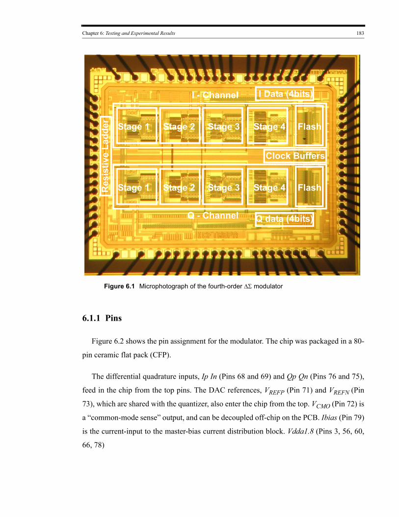
Chapter 6: Testing and Experimental Results 183
I - Channel
Stage 1 Stage 2 Stage 3 Stage 4 Flash
Q - Channel
Res
istiv
e La
dder
Clock Buffers
I Data (4bits)
Q data (4bits)
FlashStage 1 Stage 2 Stage 3 Stage 4
Figure 6.1 Microphotograph of the fourth-order ΔΣ modulator
6.1.1 Pins
Figure 6.2 shows the pin assignment for the modulator. The chip was packaged in a 80-
pin ceramic flat pack (CFP).
The differential quadrature inputs, Ip In (Pins 68 and 69) and Qp Qn (Pins 76 and 75),
feed in the chip from the top pins. The DAC references, VREFP (Pin 71) and VREFN (Pin
73), which are shared with the quantizer, also enter the chip from the top. VCMO (Pin 72) is
a “common-mode sense” output, and can be decoupled off-chip on the PCB. Ibias (Pin 79)
is the current-input to the master-bias current distribution block. Vdda1.8 (Pins 3, 56, 60,
66, 78)
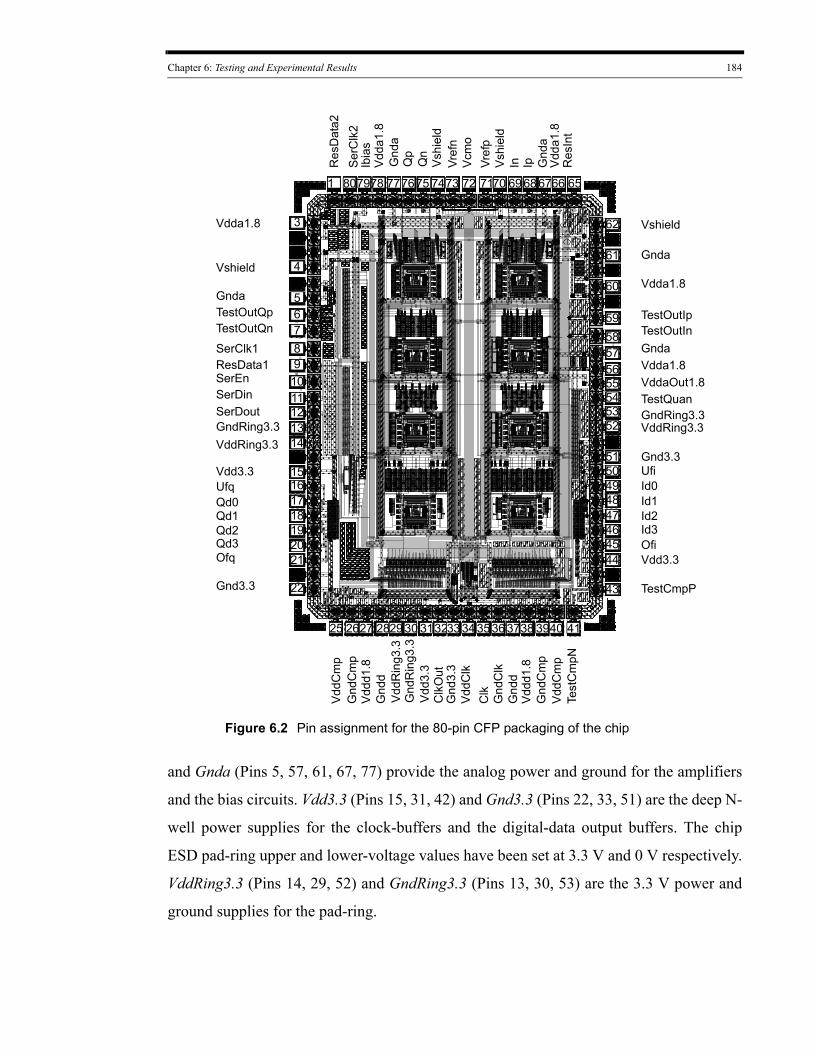
Chapter 6: Testing and Experimental Results 184
1 807978 777675 7473 72 7170 69686766 65
62
61
60
5958575655545352
5150494847464544
43
3
4
5678
1011121314
15161718192021
22
25 2627 282930 3132333435363738 3940 41
Vdda1.8
Vshield
GndaTestOutQpTestOutQn
SerClk1
SerEnResData1
SerDinSerDoutGndRing3.3VddRing3.3
UfqVdd3.3
Qd0Qd1Qd2
Ofq
Ibia
s
Gnd
aV
dda1
.8
Qn
Qp
Vsh
ield
Vcm
oVr
efn
Vref
pVs
hiel
dIn Ip G
nda
Vdd
a1.8
Res
Int
Ser
Clk
2R
esD
ata2
9
Qd3
Vshield
Gnda
Vdda1.8
TestOutIpTestOutInGndaVdda1.8
TestQuanVddaOut1.8
GndRing3.3VddRing3.3
Gnd3.3Ufi
Id1Id0
Id2Id3OfiVdd3.3
TestCmpP
Vddd
1.8
Vdd
Rin
g3.3
Gnd
d
Vdd
3.3
Gnd
Rin
g3.3
Clk
Out
VddC
lkG
nd3.
3
Clk
Gnd
Clk
Gnd
dVd
dd1.
8G
ndC
mp
Vdd
Cm
pTe
stC
mpN
Gnd
Cm
pV
ddC
mp
Gnd3.3
Figure 6.2 Pin assignment for the 80-pin CFP packaging of the chip
and Gnda (Pins 5, 57, 61, 67, 77) provide the analog power and ground for the amplifiers
and the bias circuits. Vdd3.3 (Pins 15, 31, 42) and Gnd3.3 (Pins 22, 33, 51) are the deep N-
well power supplies for the clock-buffers and the digital-data output buffers. The chip
ESD pad-ring upper and lower-voltage values have been set at 3.3 V and 0 V respectively.
VddRing3.3 (Pins 14, 29, 52) and GndRing3.3 (Pins 13, 30, 53) are the 3.3 V power and
ground supplies for the pad-ring.
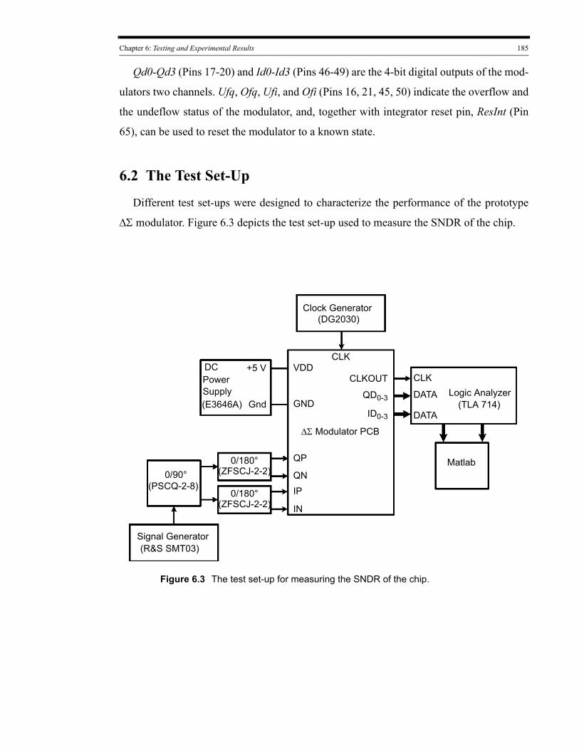
Chapter 6: Testing and Experimental Results 185
Qd0-Qd3 (Pins 17-20) and Id0-Id3 (Pins 46-49) are the 4-bit digital outputs of the mod-
ulators two channels. Ufq, Ofq, Ufi, and Ofi (Pins 16, 21, 45, 50) indicate the overflow and
the undeflow status of the modulator, and, together with integrator reset pin, ResInt (Pin
65), can be used to reset the modulator to a known state.
6.2 The Test Set-Up
Different test set-ups were designed to characterize the performance of the prototype
ΔΣ modulator. Figure 6.3 depicts the test set-up used to measure the SNDR of the chip.
Logic Analyzer
Matlab
ΔΣ Modulator PCB
Clock Generator
Signal Generator
DC
SupplyPower CLK
DATA
DATA
(DG2030)
(TLA 714)
(R&S SMT03)
0/90°0/180°
0/180°
(ZFSCJ-2-2)
(ZFSCJ-2-2)
(PSCQ-2-8)
(E3646A)
+5 V
Gnd
CLKVDD
GNDQD0-3
ID0-3
CLKOUT
QP
QNIP
IN
Figure 6.3 The test set-up for measuring the SNDR of the chip.
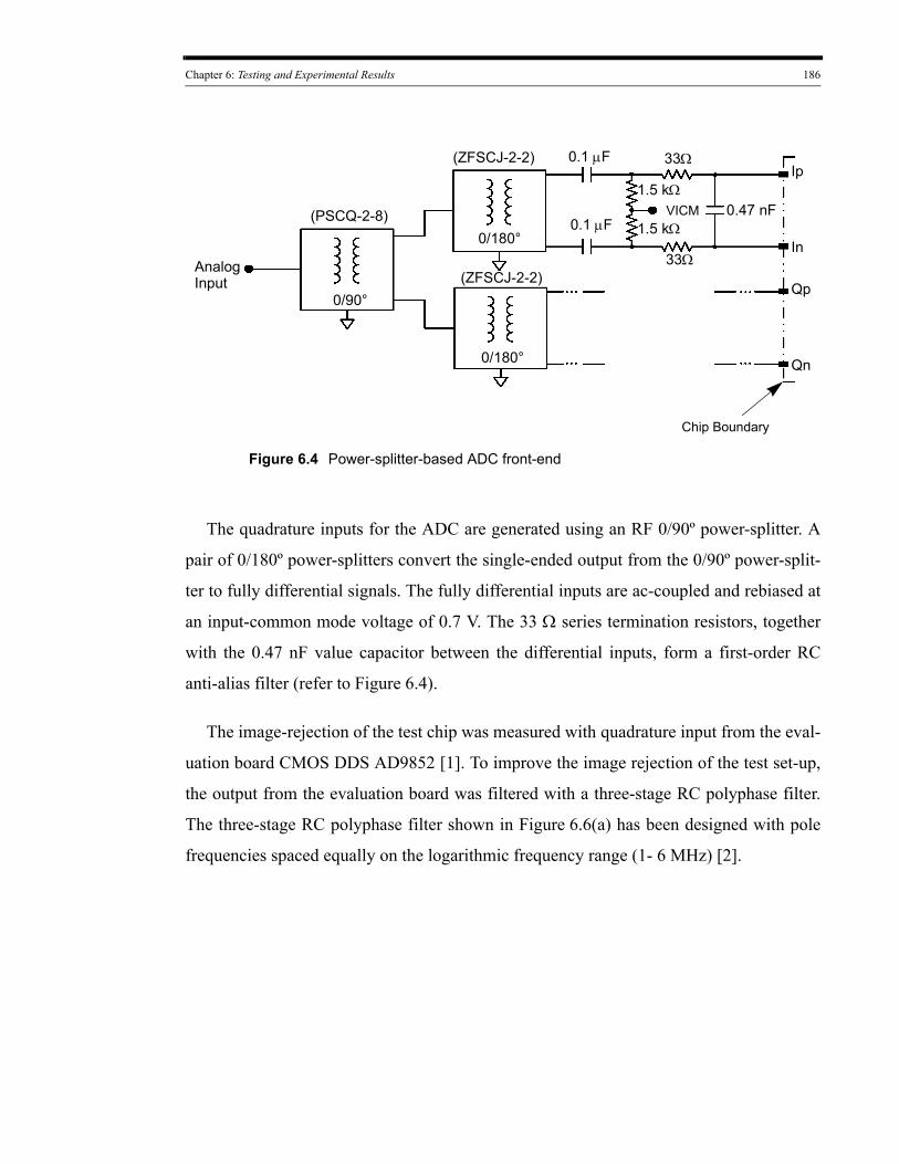
Chapter 6: Testing and Experimental Results 186
Figure 6.4 Power-splitter-based ADC front-end
Ip
In
Qp
Qn
(ZFSCJ-2-2) 0.1 μF
0.1 μF
AnalogInput
1.5 kΩ
1.5 kΩ0.47 nF
Chip Boundary
VICM
33Ω
33Ω
0/180°
0/180°
0/90°(ZFSCJ-2-2)
(PSCQ-2-8)
The quadrature inputs for the ADC are generated using an RF 0/90º power-splitter. A
pair of 0/180º power-splitters convert the single-ended output from the 0/90º power-split-
ter to fully differential signals. The fully differential inputs are ac-coupled and rebiased at
an input-common mode voltage of 0.7 V. The 33 Ω series termination resistors, together
with the 0.47 nF value capacitor between the differential inputs, form a first-order RC
anti-alias filter (refer to Figure 6.4).
The image-rejection of the test chip was measured with quadrature input from the eval-
uation board CMOS DDS AD9852 [1]. To improve the image rejection of the test set-up,
the output from the evaluation board was filtered with a three-stage RC polyphase filter.
The three-stage RC polyphase filter shown in Figure 6.6(a) has been designed with pole
frequencies spaced equally on the logarithmic frequency range (1- 6 MHz) [2].
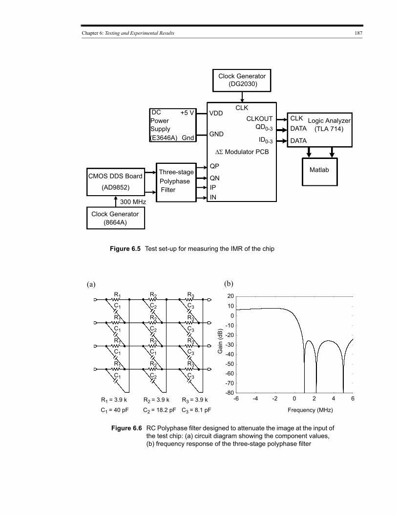
Chapter 6: Testing and Experimental Results 187
Logic Analyzer
Matlab
ΔΣ Modulator PCB
Clock Generator
DC
SupplyPower CLK
DATA
DATA
(DG2030)
(TLA 714)(E3646A)
+5 V
Gnd
CLKVDD
GNDQD0-3
ID0-3
CLKOUT
QP
QNIPIN
CMOS DDS Board Three-stagePolyphaseFilter
Figure 6.5 Test set-up for measuring the IMR of the chip
Clock Generator(8664A)
(AD9852)
300 MHz
Figure 6.6 RC Polyphase filter designed to attenuate the image at the input of the test chip: (a) circuit diagram showing the component values, (b) frequency response of the three-stage polyphase filter
R1
R1
R1
R1
C1
C1
C1
C1
Gai
n (d
B)
-70-60-50-40-30-20-10
0
10
-80
Frequency (MHz)
0 2 4 6-2-4-6
20R2
R2
R2
R2
C2
C2
C1
C2
R3
R3
R3
R3
C3
C3
C3
C3
(a) (b)
R3 = 3.9 k
C3 = 8.1 pF
R2 = 3.9 k
C2 = 18.2 pF
R1 = 3.9 k
C1 = 40 pF
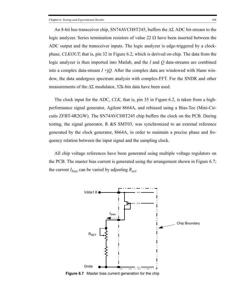
Chapter 6: Testing and Experimental Results 188
An 8-bit bus transceiver chip, SN74AVCH8T245, buffers the ΔΣ ADC bit-stream to the
logic analyzer. Series termination resistors of value 22 Ω have been inserted between the
ADC output and the transceiver inputs. The logic analyzer is edge-triggered by a clock-
phase, CLKOUT, that is, pin 32 in Figure 6.2, which is derived on-chip. The data from the
logic analyzer is then imported into Matlab, and the I and Q data-streams are combined
into a complex data-stream I +jQ. After the complex data are windowed with Hann win-
dow, the data undergoes spectrum analysis with complex-FFT. For the SNDR and other
measurements of the ΔΣ modulator, 32k-bin data have been used.
The clock input for the ADC, CLK, that is, pin 35 in Figure 6.2, is taken from a high-
performance signal generator, Agilent 8664A, and rebiased using a Bias-Tee (Mini-Cir-
cuits ZFBT-4R2GW). The SN74AVCH8T245 chip buffers the clock on the PCB. During
testing, the signal generator, R &S SMT03, was synchronized to an external reference
generated by the clock generator, 8664A, in order to maintain a precise phase and fre-
quency relation between the input signal and the sampling clock.
All chip voltage references have been generated using multiple voltage regulators on
the PCB. The master bias current is generated using the arrangement shown in Figure 6.7;
the current Ibias can be varied by adjusting Rset.
RSET
Vdda1.8
Gnda
Chip Boundary
Ibias
Figure 6.7 Master bias current generation for the chip
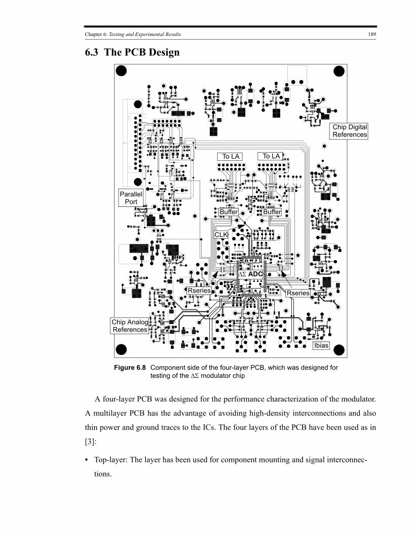
Chapter 6: Testing and Experimental Results 189
6.3 The PCB Design
Figure 6.8 Component side of the four-layer PCB, which was designed for testing of the ΔΣ modulator chip
ΔΣ ADC
Buffer Buffer
CLK
Rseries
ParallelPort
Chip AnalogReferences
Rseries
Ibias
To LA To LA
Chip DigitalReferences
A four-layer PCB was designed for the performance characterization of the modulator.
A multilayer PCB has the advantage of avoiding high-density interconnections and also
thin power and ground traces to the ICs. The four layers of the PCB have been used as in
[3]:
• Top-layer: The layer has been used for component mounting and signal interconnec-
tions.
Chapter 6: Testing and Experimental Results 190
• Power plane: The power plane has been split into multiple planes associated with the
analog, digital, and clock-generator supplies.
• Ground plane: One layer of the PCB has been dedicated to the ground plane.
• Bottom-layer: The layer has been used for some of the non-critical component mount-
ing and some interconnections.
Two PCBs were designed for the testing of the chip. In the first PCB design, the ground
plane was split into two sub-planes separating the analog ground from the digital ground
and the two planes were finally joined at the power supply. In the second PCB design, the
undivided ground plane was shared between the analog and the digital grounds. Compared
to the first PCB, the second PCB was less noisy, and this fact was confirmed by the SNDR
measurements of the chip. The second PCB showed an improvement of 3 dB in SNDR, as
compared to the first PCB. A possible reason for the degraded performance of the first
PCB could be that the digital ground impedance for the split ground plane was on the
higher side, and this higher impedance was causing a crossover of the digital noise to the
analog ground. In the second PCB, instead of splitting the ground plane, an effort was
made to partition the routes into analog and digital sections. The component placement
and layout was done in such a way to prevent cross-over of routes from one section to the
other section.
Supply decoupling for the chip is achieved through a hierarchical placement of on-chip
and on-PCB capacitors. The off-chip decoupling is performed using two types of surface-
mounted capacitors: a bank of large electrolytic capacitors of value 100 nF and a bank of
smaller ceramic capacitors of value 10 nF [4]. The ceramic capacitors are placed closer to
the power pins in order to minimize the impact of parasitic lead-inductance. The decou-
pling capacitors, local as well as global, are connected to the ground and the power plane
through interconnects of minimal lengths and, hence, of minimal parasitic inductances.
Signal crossing, wherever it could not be avoided, is provided with a nearby decoupling
capacitor between the power and the ground plane [5].
The chip is directly soldered to the PCB. The differential inputs to the ADC are
matched in length and placed close together. Special precautions are taken to keep the dig-
Chapter 6: Testing and Experimental Results 191
ital signal traces, especially the clock signal, as far away as possible from the analog
inputs and supply pins. The clock signal is routed on the top-layer, and care is taken to
avoid crossing clock routes to the bottom-layer of the PCB.
6.4 Test Results
The test results of the proposed ΔΣ modulator are very close to the simulated results,
except for a somewhat reduced maximum sampling frequency. Due to some SNR degra-
dation issues between 105MHz and the maximum sampling frequency of 128 MHz, the
ADC testing was limited to a sampling frequency of 96 MHz. The IC achieved 70.9 dB
SNDR over a 6 MHz band centered around 3 MHz. At 105 MHz, the IC performs with a
loss of 3 dB in the SNDR.
Figure 6.9 shows the STF plot of the proposed ΔΣ ADC, which is measured at a sam-
pling frequency of 96 MHz. The asymmetric shape of the STF plot is evident from this
figure. The notch at dc in the STF plot has been caused by ac-coupling.
Figure 6.10 shows the output PSD of the chip measured for zero-input. The output
spectrum reveals the complex noise shaping of the modulator and the deep notch that has
been placed at the image frequency. A plot of the measured SNDR versus input amplitude
is shown in Figure 6.11. The modulator shows a dynamic range of about 75 dB for an
input bandwidth of 6 MHz and a sampling frequency of 96 MHz. The modulator shows a
maximum SNDR of about 71 dB for a 6 MHz input frequency at an amplitude of -3 dBFS
(refer to Figure 6.12).
Using a CMOS DDS evaluation board, AD9852, as a quadrature signal source, the
image rejection of the IC was measured at a several frequencies within the 6 MHz signal
bandwidth (refer to Figure 6.5 for the test set-up used to measure the IMR of the IC). A
three-stage polyphase filter was used at the IC front-end to suppress the phase and gain
imbalances due to the DDS (refer to Figure 6.6 for the details of the polyphase filter). Due
to the narrow band limitation of the polyphase filter, the frequency of the input signal for
the image rejection measurement was restricted to a range between 2.75 MHz and 4.5
MHz. Figure 6.13 shows the output spectrum of the ΔΣ modulator for a –3 MHz input sig-
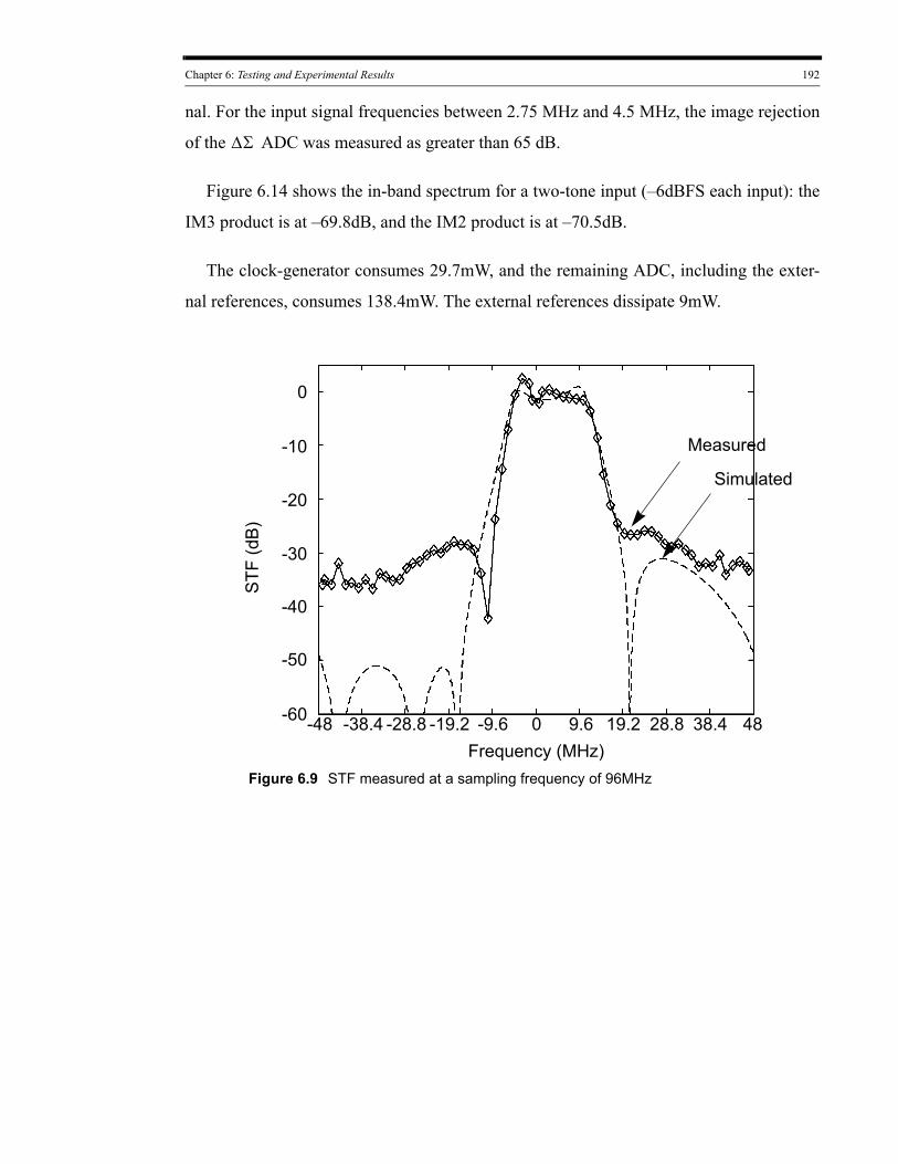
Chapter 6: Testing and Experimental Results 192
nal. For the input signal frequencies between 2.75 MHz and 4.5 MHz, the image rejection
of the ΔΣ ADC was measured as greater than 65 dB.
Figure 6.14 shows the in-band spectrum for a two-tone input (–6dBFS each input): the
IM3 product is at –69.8dB, and the IM2 product is at –70.5dB.
The clock-generator consumes 29.7mW, and the remaining ADC, including the exter-
nal references, consumes 138.4mW. The external references dissipate 9mW.
-40
-30
-20
-10
0
-9.6 0 9.6 19.2 28.8 38.4-38.4-48 -28.8 -19.2 48Frequency (MHz)
STF
(dB
)
Figure 6.9 STF measured at a sampling frequency of 96MHz
Measured
Simulated
-50
-60
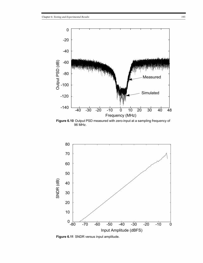
Chapter 6: Testing and Experimental Results 193
Figure 6.10 Output PSD measured with zero-input at a sampling frequency of 96 MHz.
-10 0 10 20 30 40-40 -30 -20 48Frequency (MHz)
-140
-80
-100
-60
-40
-20
0
Out
put P
SD
(dB
)
-120
Measured
Simulated
10
20
30
40
50
60
70
80
-60 -50 -40 -30 -20 -10-80 -70 0Input Amplitude (dBFS)
SN
DR
(dB
)
Figure 6.11 SNDR versus input amplitude.
0
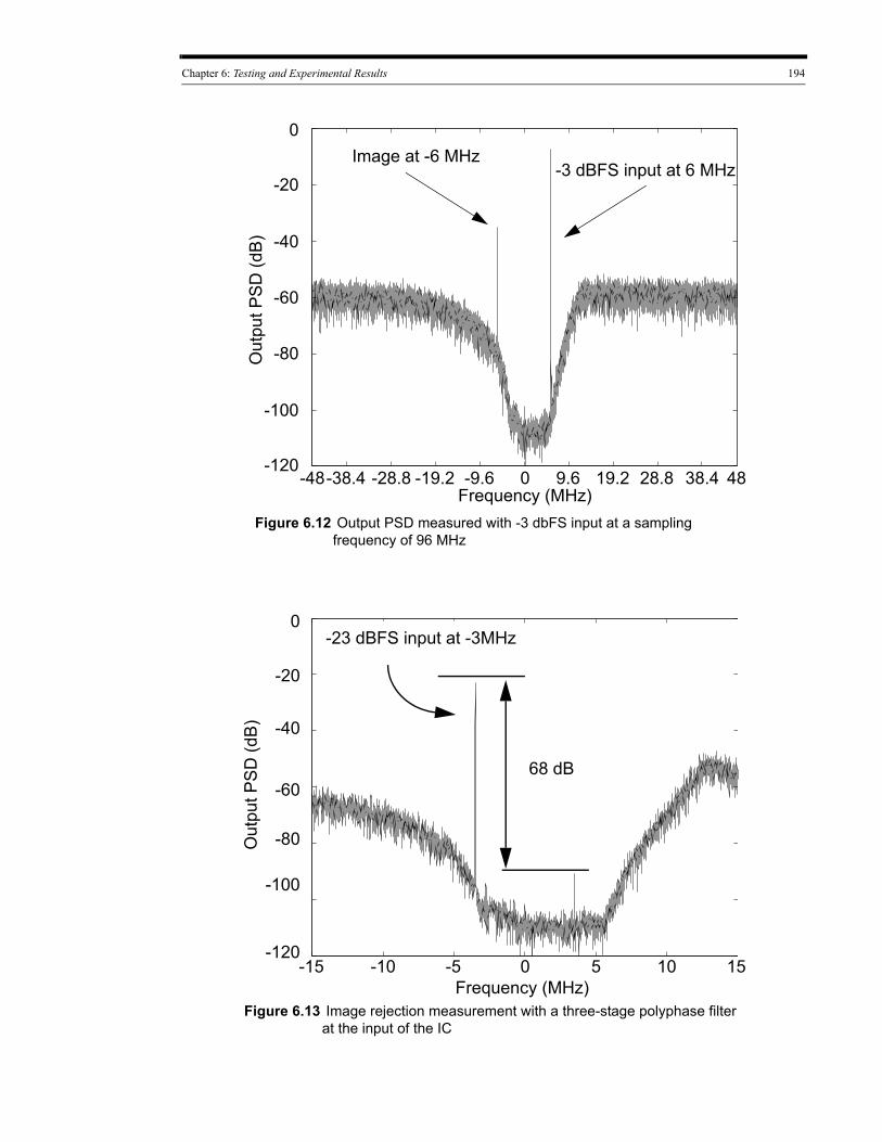
Chapter 6: Testing and Experimental Results 194
Figure 6.12 Output PSD measured with -3 dbFS input at a sampling frequency of 96 MHz
-9.6 0 9.6 19.2 28.8 38.4-38.4-48 -28.8 -19.2 48Frequency (MHz)
-120
-80
-100
-60
-40
-20
0
Out
put P
SD
(dB
)
-3 dBFS input at 6 MHzImage at -6 MHz
68 dB
5-10 0
-20
-40
0
-80
-60
-100
-120
Frequency (MHz)-5 10
Out
put P
SD
(dB
)
Figure 6.13 Image rejection measurement with a three-stage polyphase filter at the input of the IC
-23 dBFS input at -3MHz
-15 15
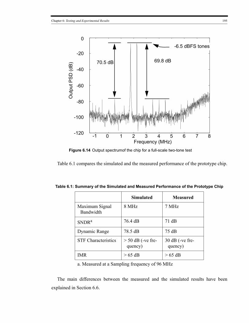
Chapter 6: Testing and Experimental Results 195
-120
-100
-40
-20
2 3 4 5 6 710Frequency (MHz)
Out
put P
SD
(dB
)
0
-80
-60
8
69.8 dB70.5 dB
-6.5 dBFS tones
Figure 6.14 Output spectrumof the chip for a full-scale two-tone test
-1
Table 6.1 compares the simulated and the measured performance of the prototype chip.
Table 6.1: Summary of the Simulated and Measured Performance of the Prototype Chip
Simulated Measured
Maximum Signal Bandwidth
8 MHz 7 MHz
SNDRa 76.4 dB 71 dB
Dynamic Range 78.5 dB 75 dB
STF Characteristics > 50 dB (-ve fre-quency)
30 dB (-ve fre-quency)
IMR > 65 dB > 65 dB
a. Measured at a Sampling frequency of 96 MHz
The main differences between the measured and the simulated results have been
explained in Section 6.6.
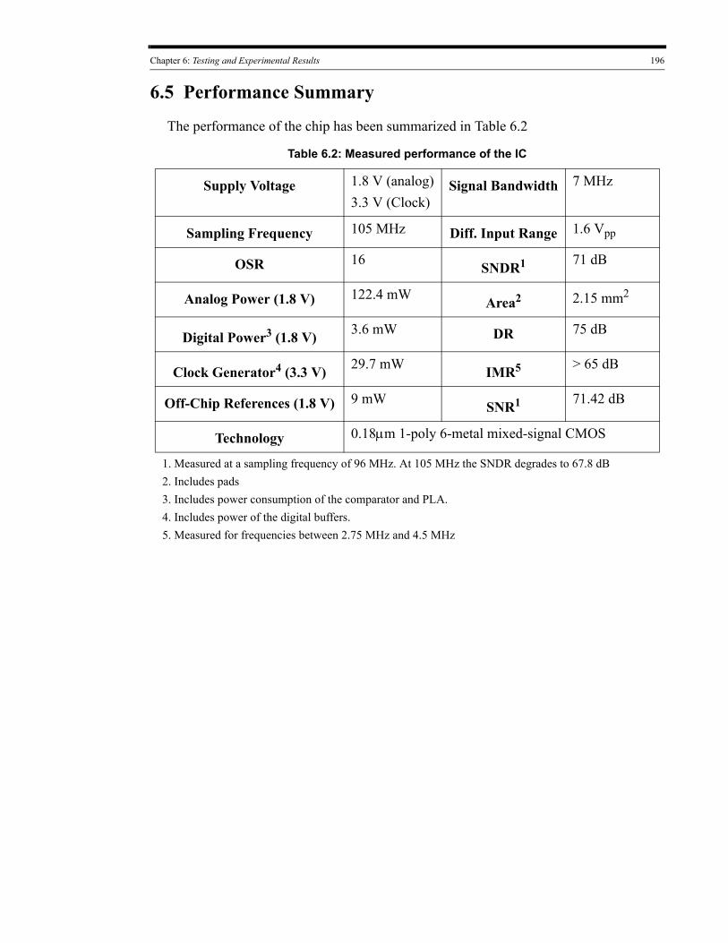
Chapter 6: Testing and Experimental Results 196
6.5 Performance Summary
The performance of the chip has been summarized in Table 6.2
Table 6.2: Measured performance of the IC
Supply Voltage 1.8 V (analog)3.3 V (Clock)
Signal Bandwidth 7 MHz
Sampling Frequency 105 MHz Diff. Input Range 1.6 Vpp
OSR 16 SNDR1
1. Measured at a sampling frequency of 96 MHz. At 105 MHz the SNDR degrades to 67.8 dB
71 dB
Analog Power (1.8 V) 122.4 mW Area2
2. Includes pads
2.15 mm2
Digital Power3
3. Includes power consumption of the comparator and PLA.
(1.8 V) 3.6 mW DR 75 dB
Clock Generator4
4. Includes power of the digital buffers.
(3.3 V) 29.7 mW IMR5
5. Measured for frequencies between 2.75 MHz and 4.5 MHz
> 65 dB
Off-Chip References (1.8 V) 9 mW SNR1 71.42 dB
Technology 0.18μm 1-poly 6-metal mixed-signal CMOS
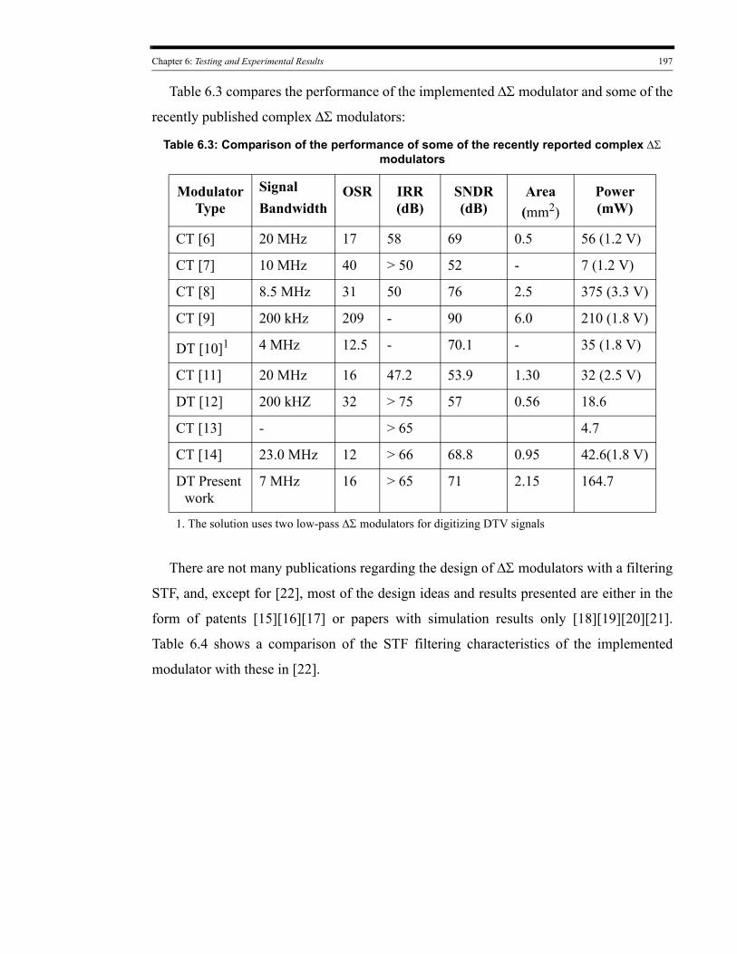
Chapter 6: Testing and Experimental Results 197
Table 6.3 compares the performance of the implemented ΔΣ modulator and some of the
recently published complex ΔΣ modulators:
Table 6.3: Comparison of the performance of some of the recently reported complex ΔΣ modulators
Modulator Type
Signal Bandwidth
OSR IRR (dB)
SNDR (dB)
Area(mm2)
Power (mW)
CT [6] 20 MHz 17 58 69 0.5 56 (1.2 V)
CT [7] 10 MHz 40 > 50 52 - 7 (1.2 V)
CT [8] 8.5 MHz 31 50 76 2.5 375 (3.3 V)
CT [9] 200 kHz 209 - 90 6.0 210 (1.8 V)
DT [10]1
1. The solution uses two low-pass ΔΣ modulators for digitizing DTV signals
4 MHz 12.5 - 70.1 - 35 (1.8 V)
CT [11] 20 MHz 16 47.2 53.9 1.30 32 (2.5 V)
DT [12] 200 kHZ 32 > 75 57 0.56 18.6
CT [13] - > 65 4.7
CT [14] 23.0 MHz 12 > 66 68.8 0.95 42.6(1.8 V)
DT Present work
7 MHz 16 > 65 71 2.15 164.7
There are not many publications regarding the design of ΔΣ modulators with a filtering
STF, and, except for [22], most of the design ideas and results presented are either in the
form of patents [15][16][17] or papers with simulation results only [18][19][20][21].
Table 6.4 shows a comparison of the STF filtering characteristics of the implemented
modulator with these in [22].
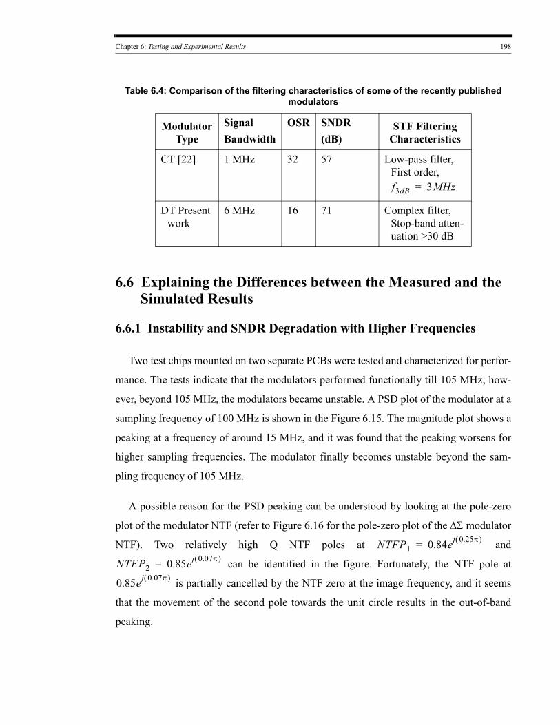
Chapter 6: Testing and Experimental Results 198
Table 6.4: Comparison of the filtering characteristics of some of the recently published modulators
Modulator Type
Signal Bandwidth
OSR SNDR(dB)
STF Filtering Characteristics
CT [22] 1 MHz 32 57 Low-pass filter, First order, f3dB 3MHz=
DT Present work
6 MHz 16 71 Complex filter, Stop-band atten-uation >30 dB
6.6 Explaining the Differences between the Measured and the Simulated Results
6.6.1 Instability and SNDR Degradation with Higher Frequencies
Two test chips mounted on two separate PCBs were tested and characterized for perfor-
mance. The tests indicate that the modulators performed functionally till 105 MHz; how-
ever, beyond 105 MHz, the modulators became unstable. A PSD plot of the modulator at a
sampling frequency of 100 MHz is shown in the Figure 6.15. The magnitude plot shows a
peaking at a frequency of around 15 MHz, and it was found that the peaking worsens for
higher sampling frequencies. The modulator finally becomes unstable beyond the sam-
pling frequency of 105 MHz.
A possible reason for the PSD peaking can be understood by looking at the pole-zero
plot of the modulator NTF (refer to Figure 6.16 for the pole-zero plot of the ΔΣ modulator
NTF). Two relatively high Q NTF poles at NTFP1 0.84ej 0.25π( )= and
NTFP2 0.85ej 0.07π( )= can be identified in the figure. Fortunately, the NTF pole at
0.85ej 0.07π( ) is partially cancelled by the NTF zero at the image frequency, and it seems
that the movement of the second pole towards the unit circle results in the out-of-band
peaking.
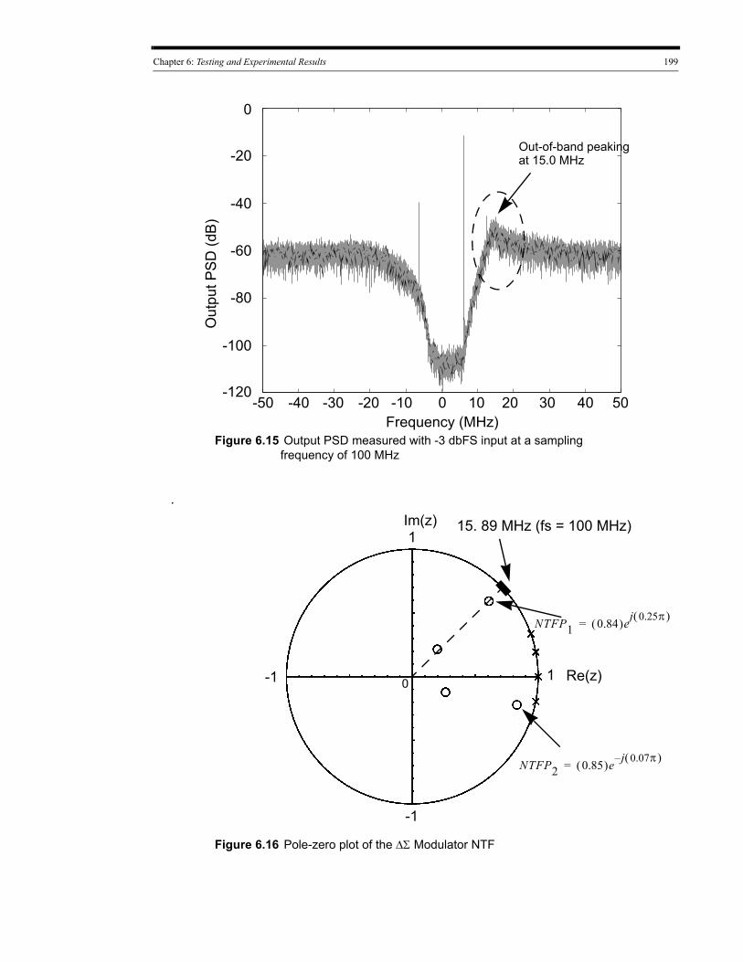
Chapter 6: Testing and Experimental Results 199
Figure 6.15 Output PSD measured with -3 dbFS input at a sampling frequency of 100 MHz
-10 0 10 20 30 40-40-50 -30 -20 50Frequency (MHz)
-120
-80
-100
-60
-40
-20
0
Out
put P
SD
(dB
)
Out-of-band peakingat 15.0 MHz
.
Figure 6.16 Pole-zero plot of the ΔΣ Modulator NTF
1-1
1
-1
Im(z)
Re(z)0
15. 89 MHz (fs = 100 MHz)
NTFP1 0.84( )ej 0.25π( )=
NTFP2 0.85( )e j– 0.07π( )=
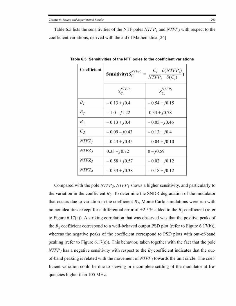
Chapter 6: Testing and Experimental Results 200
Table 6.5 lists the sensitivities of the NTF poles NTFP1 and NTFP2 with respect to the
coefficient variations, derived with the aid of Mathematica [24]
Table 6.5: Sensitivities of the NTF poles to the coefficient variations
CoefficientSensitivity(SCi
NTFPi CiNTFPi-----------------
∂ NTFPi( )∂ Ci( )
-------------------------= )
SCi
NTFP1 SCi
NTFP2
B1 0.13– j0.4+ 0.54– j0.15+
B2 1.0– j1.22– 0.33 j0.78+
B3 0.13– j0.4+ 0.05– j0.46–
C2 0.09– j0.43– 0.13– j0.4+
NTFZ1 0.43– j0.45+ 0.04– j0.10+
NTFZ2 0.33 j0.72– 0 j0.59–
NTFZ3 0.58– j0.57+ 0.02– j0.12+
NTFZ4 0.33– j0.38+ 0.18– j0.12+
Compared with the pole NTFP2, NTFP1 shows a higher sensitivity, and particularly to
the variation in the coefficient B2. To determine the SNDR degradation of the modulator
that occurs due to variation in the coefficient B2, Monte Carlo simulations were run with
no nonidealities except for a differential error of 2.5± % added to the B2 coefficient (refer
to Figure 6.17(a)). A striking correlation that was observed was that the positive peaks of
the B2 coefficient correspond to a well-behaved output PSD plot (refer to Figure 6.17(b)),
whereas the negative peaks of the coefficient correspond to PSD plots with out-of-band
peaking (refer to Figure 6.17(c)). This behavior, taken together with the fact that the pole
NTFP1 has a negative sensitivity with respect to the B2 coefficient indicates that the out-
of-band peaking is related with the movement of NTFP1 towards the unit circle. The coef-
ficient variation could be due to slewing or incomplete settling of the modulator at fre-
quencies higher than 105 MHz.
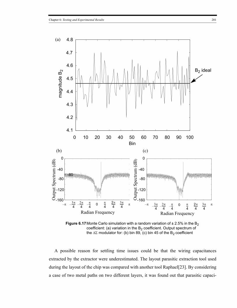
Chapter 6: Testing and Experimental Results 201
40 50 60 70 80 90100 20 30 100Bin
4.2
4.1
4.3
4.4
4.5
4.6m
agni
tude
B2
Figure 6.17Monte Carlo simulation with a random variation of ± 2.5% in the B2 coefficient: (a) variation in the B2 coefficient. Output spectrum of the ΔΣ modulator for: (b) bin 89, (c) bin 45 of the B2 coefficient
4.7
4.8
B2 ideal
-40-80
0
-120
-160
Radian Frequency
Out
put S
pect
rum
(dB
)
0
-80
-40
0
-120
-160Out
put S
pect
rum
(dB
)
-80
π4--- 2π
4------ 3π
4------ ππ
4---–2π
4------–3π
4------–π–
Radian Frequency
0 π4--- 2π
4------ 3π
4------ ππ
4---–2π
4------–3π
4------–π–
(a)
(b) (c)
A possible reason for settling time issues could be that the wiring capacitances
extracted by the extractor were underestimated. The layout parasitic extraction tool used
during the layout of the chip was compared with another tool Raphael[23]. By considering
a case of two metal paths on two different layers, it was found out that parasitic capaci-
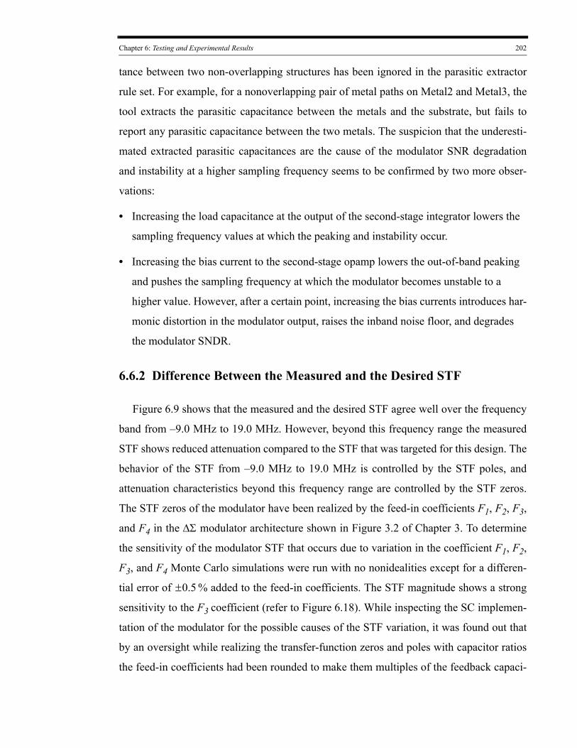
Chapter 6: Testing and Experimental Results 202
tance between two non-overlapping structures has been ignored in the parasitic extractor
rule set. For example, for a nonoverlapping pair of metal paths on Metal2 and Metal3, the
tool extracts the parasitic capacitance between the metals and the substrate, but fails to
report any parasitic capacitance between the two metals. The suspicion that the underesti-
mated extracted parasitic capacitances are the cause of the modulator SNR degradation
and instability at a higher sampling frequency seems to be confirmed by two more obser-
vations:
• Increasing the load capacitance at the output of the second-stage integrator lowers the
sampling frequency values at which the peaking and instability occur.
• Increasing the bias current to the second-stage opamp lowers the out-of-band peaking
and pushes the sampling frequency at which the modulator becomes unstable to a
higher value. However, after a certain point, increasing the bias currents introduces har-
monic distortion in the modulator output, raises the inband noise floor, and degrades
the modulator SNDR.
6.6.2 Difference Between the Measured and the Desired STF
Figure 6.9 shows that the measured and the desired STF agree well over the frequency
band from –9.0 MHz to 19.0 MHz. However, beyond this frequency range the measured
STF shows reduced attenuation compared to the STF that was targeted for this design. The
behavior of the STF from –9.0 MHz to 19.0 MHz is controlled by the STF poles, and
attenuation characteristics beyond this frequency range are controlled by the STF zeros.
The STF zeros of the modulator have been realized by the feed-in coefficients F1, F2, F3,
and F4 in the ΔΣ modulator architecture shown in Figure 3.2 of Chapter 3. To determine
the sensitivity of the modulator STF that occurs due to variation in the coefficient F1, F2,
F3, and F4 Monte Carlo simulations were run with no nonidealities except for a differen-
tial error of 0.5± % added to the feed-in coefficients. The STF magnitude shows a strong
sensitivity to the F3 coefficient (refer to Figure 6.18). While inspecting the SC implemen-
tation of the modulator for the possible causes of the STF variation, it was found out that
by an oversight while realizing the transfer-function zeros and poles with capacitor ratios
the feed-in coefficients had been rounded to make them multiples of the feedback capaci-
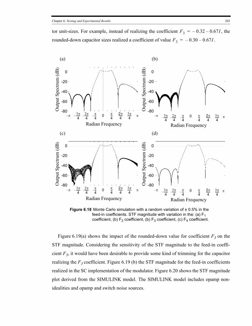
Chapter 6: Testing and Experimental Results 203
tor unit-sizes. For example, instead of realizing the coefficient F3 0.32– 0.67I–= , the
rounded-down capacitor sizes realized a coefficient of value F3 0.30– 0.67I–= .
Figure 6.18 Monte Carlo simulation with a random variation of ± 0.5% in the feed-in coefficients. STF magnitude with variation in the: (a) F1 coefficient, (b) F2 coefficient, (b) F3 coefficient, (c) F4 coefficient.
Radian Frequency
Out
put S
pect
rum
(dB
)
0
Out
put S
pect
rum
(dB
)
π4--- 2π
4------ 3π
4------ ππ
4---–2π
4------–3π
4------–π–
Radian Frequency
0 π4--- 2π
4------ 3π
4------ ππ
4---–2π
4------–3π
4------–π–
(c) (d)
-20
0
-60
-80
Radian Frequency
Out
put S
pect
rum
(dB
)
0
-40
Out
put S
pect
rum
(dB
)
π4--- 2π
4------ 3π
4------ ππ
4---–2π
4------–3π
4------–π–
Radian Frequency
0 π4--- 2π
4------ 3π
4------π
4---–2π
4------–3π
4------–π–
(a) (b)
π
-20
0
-60
-80
-40
-20
0
-60
-80
-40
-20
0
-60
-80
-40
Figure 6.19(a) shows the impact of the rounded-down value for coefficient F3 on the
STF magnitude. Considering the sensitivity of the STF magnitude to the feed-in coeffi-
cient F3, it would have been desirable to provide some kind of trimming for the capacitor
realizing the F3 coefficient. Figure 6.19 (b) the STF magnitude for the feed-in coefficients
realized in the SC implementation of the modulator. Figure 6.20 shows the STF magnitude
plot derived from the SIMULINK model. The SIMULINK model includes opamp non-
idealities and opamp and switch noise sources.
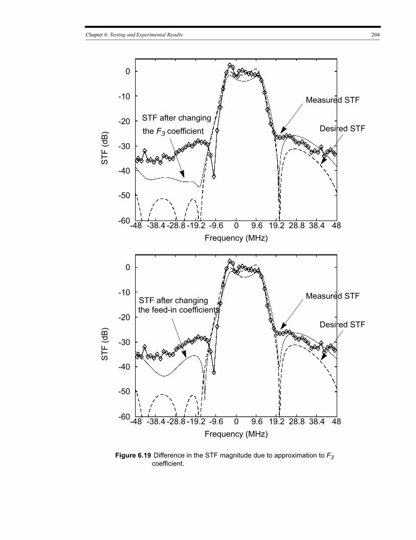
Chapter 6: Testing and Experimental Results 204
-9.6 0 9.6 19.2 28.8 38.4-38.4-48 -28.8 -19.2 48Frequency (MHz)
STF
(dB
)
Figure 6.19 Difference in the STF magnitude due to approximation to F3 coefficient.
Measured STF
Desired STFSTF after changing the F3 coefficient
-40
-30
-20
-10
0
-50
-60
-9.6 0 9.6 19.2 28.8 38.4-38.4-48 -28.8 -19.2 48Frequency (MHz)
STF
(dB
)
Measured STF
Desired STF
STF after changing
-40
-30
-20
-10
0
-50
-60
the feed-in coefficients
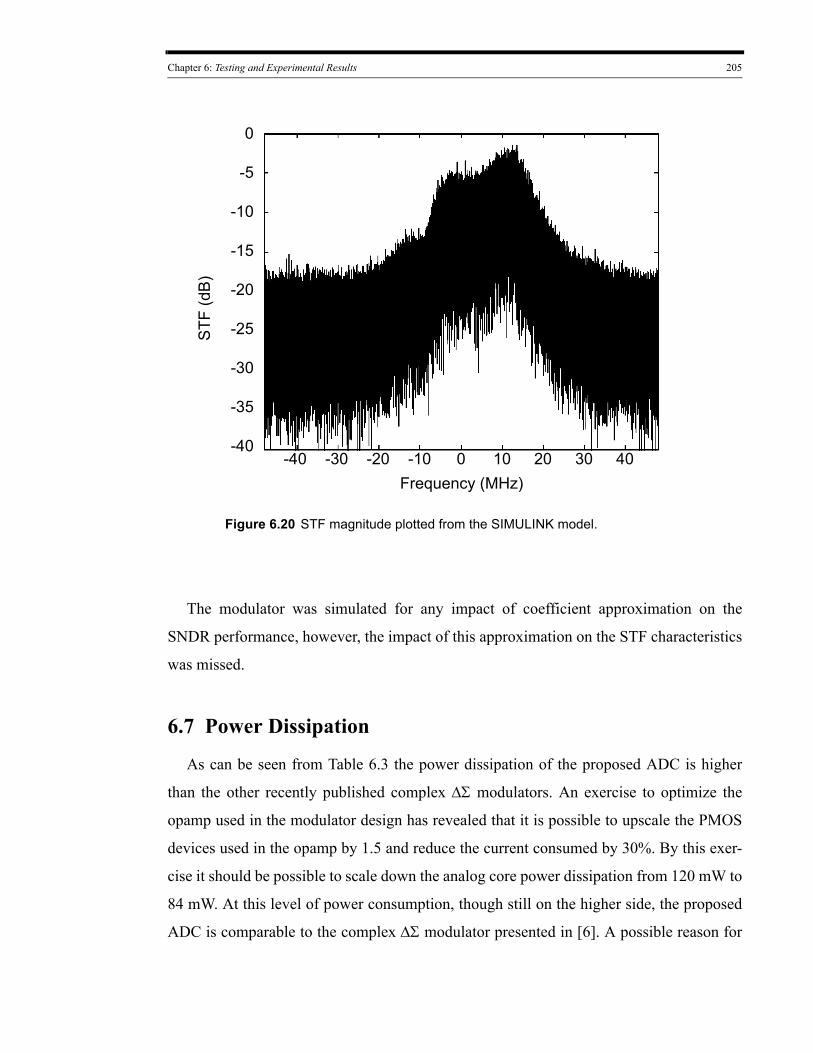
Chapter 6: Testing and Experimental Results 205
-10 0 10 20 30 40-40 -30 -20Frequency (MHz)
STF
(dB
)
Figure 6.20 STF magnitude plotted from the SIMULINK model.
-20
-15
-10
-5
0
-25
-30
-35
-40
The modulator was simulated for any impact of coefficient approximation on the
SNDR performance, however, the impact of this approximation on the STF characteristics
was missed.
6.7 Power Dissipation
As can be seen from Table 6.3 the power dissipation of the proposed ADC is higher
than the other recently published complex ΔΣ modulators. An exercise to optimize the
opamp used in the modulator design has revealed that it is possible to upscale the PMOS
devices used in the opamp by 1.5 and reduce the current consumed by 30%. By this exer-
cise it should be possible to scale down the analog core power dissipation from 120 mW to
84 mW. At this level of power consumption, though still on the higher side, the proposed
ADC is comparable to the complex ΔΣ modulator presented in [6]. A possible reason for
Chapter 6: Testing and Experimental Results 206
higher power consumption could be the larger capacitors used to realize the coefficients of
the modulator. This was done so that the matching between the two channels (I and Q)
remains high. The IMR measurement results of the proposed ADC confirm superior
matching of the I and Q channels.
Chapter 6: Testing and Experimental Results 207
References[1] Analog Devices Inc., AD9852: CMOS 300 MSPS Complete DDS.
[2] F. Behbahani, A. Karimi-Sanjaani, Wee-Guan Tan, A. Roithmeier, J.C. Leete, K. Hoshino, A. A. Abidi, “CMOS mixers and polyphase filters for large image rejection,” IEEE Journal of Solid-State Circuits, Vol. 36, Issue. 8, pp. 873–887, June 2001.
[3] Mark I. Montrose, EMC and Printed Circuit Board: Design, Theory, and layout Made Simple (1st Edition), ISBN 078034703X, Wiley-IEEE Press, 1998.
[4] L. D. Smith, R. E. Anderson, D. W. Forehand, T. J. Pelc, T. Roy, “Power distribution system design methodology and capacitor selection for modern CMOS technology,” IEEE Transactions on Advanced Packaging, Vol. 22, Issue. 3, pp. 284–291, August 1999.
[5] Ralph Morrison, Grounding and Shielding Circuits and Interference (5th Edition), ISBN 0470097728, Wiley-IEEE Press, 2007.
[6] L. J. Breems, R. Rutten, R. van Veldhoven, G. van der Weide, H. Termeer, “A 56mW CT quadrature cascaded ΔΣ modulator with 77dB DR in a near Zero-IF 20MHz band,” ISSCC Dig. Tech. Papers, pp. 238 - 599, Feb. 2007.
[7] S. Ouzounov, R. van Veldhoven, C. Bastiaansen, K. Vongehr, R. van Wegberg, G. Geelen, L. Breems, “A 1.2V 121-Mode CT ΔΣ modulator for wireless receivers in 90nm CMOS,” ISSCC Dig. Tech. Papers, pp. 242 - 600, Feb. 2007.
[8] R. Schreier, N. Abaskharoun, H. Shibata, D. Paterson, S. Rose, I. Mehr, Q. Luu, “A 375-mW Quadrature Bandpass ∆Σ ADC With 8.5-MHz BW and 90-dB DR at 44 MHz,” IEEE Journal of Solid-State Circuits, Vol. 41, Issue. 12, pp. 2632-2640, December 2006.
[9] Paulo G. R. Silva, L. J. Breems, Kofi A.A Makinawa, Raf Roovers, Johan H. Huijsing, “An 118dB DR CT IF-to-baseband ∆Σ modulator for AM/FM/IBOC radio receivers,” ISSCC Dig. Tech. Papers, pp. 66 - 637, Feb. 2006.
[10] Yoshihisa Fujimoto, Yusuke Kanazawa, Pascal Lore, Masayuki Miyamoto, “An 80/100MS/s 76.3/70.1dB SNDR ∆Σ ADC for digital TV receivers,” ISSCC Dig. Tech. Papers, pp. 76 - 639, Feb. 2006.
[11] Jesus Arias,Peter Kiss, Vladimir Prodanov, Vito Boccuzzi, Mihai Banu, David Bisbal, Jacinto San Pablo, Luis Quintanilla, and Juan Barbolla, “A 32-mW 320-MHz Continuous-Time Complex Delta-SigmaADC for Multi-Mode Wireless-LAN Receivers,” IEEE Journal of Solid-State Circuits, vol. 41, pp. 339-351, Feb 2006.
[12] Kong-Pang Pun, Wang-Tung Cheng, Chiu-Sing Choy, Cheong-Fat Chun, “A 75-dB image rejection IF-input quadrature-sampling SC ∆Σ modulator,” IEEE Journal of Solid-State Circuits, Vol. 41, Issue. 6, pp. 1353-1363, June 2006.
[13] F. Munoz, K. Philips, A. Torralba, “A 4.7mW 89.5dB DR CT complex ΔΣ ADC with built-in LPF,” ISSCC Dig. Tech. Papers, pp. 500 - 613, Feb. 2005.
Chapter 6: Testing and Experimental Results 208
[14] Navid Yaghini, David Johns, “A 43mW CT complex ΔΣ ADC with 23MHz of signal bandwidth and 68.8dB SNDR,” ISSCC Dig. Tech. Papers, pp. 502 - 613, Feb. 2005.
[15] John Laurence Melanson, “Delta-sigma modulators with integral digital low-pass filtering,” United States Patent, US 7,116,721.
[16] Yann Le Guillou, “Feedforward sigma-delta AD converter with an optimized built-in filter function,” European Patent, WO 2007/066273.
[17] Yann Le Guillou, Hussein Fakhoury, “Continuous-time sigma-delta analog-to-digital converter with non-invasive filters(s) for immunity preservation against interferers,” European Patent, WO 2006/054214.
[18] M. Ranjbar, O. Oliaei, “Continuous-time feed-forward ΣΔ- modulators with robust signal transfer function,” Electronics Letters, vol. 43, no. 24, pp. 1878-1881, 22nd November 2007.
[19] N. Jouida, N. C. Rebai, A. Ghazel, “Built-in Filtering for Out-of-Channel Interferers in Continuous-Time Quadrature Bandpass Delta Sigma Modulators,” ICECS, pp. 947-950, December 2007.
[20] Y. Le Guillou, H. Fakhoury, “Elliptic filtering in continuous-time sigma-delta modulato,” Electronics Letters, vol. 41, no. 4, pp. 167-168, 17th February 2007
[21] N. Beilleau, H. Abouushady, and M. M. Louerat, “Filtering adjacent channel blockers using signal-transfer-function of continuous-time ΔΣ modulators,” IEEE Midwest symposium on circuits and systems, July 2004.
[22] K. Philips, P.A.C.M. Nuijten, R.L.J. Roovers, A.H.M. van Roermund, F.M. Chavero, M.T. Pallares, A. Torralba, “A continuous-time ΣΔ ADC with increased immunity to interferers,” IEEE Journal of Solid-State Circuits, Vol. 39, Issue. 12, pp. 2170-2178, December 2004.
[23] Synopsys, Inc., Raphael- Interconnect Analysis Tool, Mountain View, CA.
[24] Wolfram Research, Inc., Mathematica, Version 6.0, Champaign, IL., Wolfram Research.

Chapter 6: Testing and Experimental Results 209
CHAPTER
Conclusions
A digital receiver architecture based on a new low-IF complex ΔΣ modulator with fil-
tering STF has been proposed in this thesis. A methodology for designing the filtering
STF has also been proposed. A thorough examination through simulations (Matlab, Spec-
tre, etc.,) was followed by a silicon implementation of a SC prototype modulator.
7.1 Contributions
This thesis presents an oversampling complex bandpass ΔΣ ADC with a signal transfer
function that achieves a significant filtering of interfering signals. A filtering ADC
reduces the complexity of the receiver by minimizing the requirements of analog filters in
the IF digitization path. Unlike the continuous time ΔΣ modulator ADCs discussed in the
literature, this discrete-time ΔΣ modulator ADC with an STF that significantly filters
interfering signals is the first one of its kind reported.
The ΔΣ modulator signal transfer function (STF) and noise transfer function (NTF)
have been designed using complex filter routines based on classical filter design proce-
dures. With a filtering STF and stop band attenuation greater than 30dB, the ΔΣ modulator
reduces intermodulation of the desired signal and the interfering signals at the input of the
quantizer, and also avoids feedback of the high-frequency interfering signals at the input
of the modulator.
The reported complex ΔΣ ADC is intended for DTV receiver applications. With a max-
imum intended sampling frequency of 128 MHz and an OSR of 16, the ADC has been
designed to support a maximum DTV signal bandwidth of 8MHz. The ADC has been
tested up to a maximum sampling frequency of 105 MHz. The IC achieved 70.9 dB SNDR
7
210
Chapter 7: Conclusions 211
over a 6 MHz band centered around 3MHz. The image rejection ratio (IRR) of the ΔΣ
ADC was measured as greater than 65 dB. The out-of-band rejection of the ADC has been
measured as greater than 30 dB. The key contributions of this thesis are:
• A new method for obtaining optimal NTF and STF in the design of ΔΣ modulators. The
approach uses a norm based criterion and allows an STF with the desired frequency
response specification. The technique has been applied to the cases of real and complex
ΔΣ modulator transfer function designs.
• The severe SNDR degradation in the traditional input-feedforward ΔΣ modulators in
presence of DAC non-linearities has been identified. For the input-feedforward ΔΣ
modulator, the interfering tones at the output of the quantizer remain of the same mag-
nitude as at the input.The large out-of-band quantization noise and the interfering tones
are aliased back in-band due to the DAC non-linearity resulting into a severe SNDR
degradation. The proposed ΔΣ modulator by filtering these out-of-band interfering sig-
nals shows an increased robustness to DAC non-linearities.
• A feedforward ΔΣ modulator architecture without the limitations of the traditional
feedforward architectures has been proposed. The architecture avoids weighted sum-
mation at the quantizer input. The STF of the modulator is well controlled and robust in
present of mismatches and other non-linearity. The well controlled bandpass nature of
the STF makes the ADC ideal for wireless signals.
• Chapter 4 and 5 discuss the behavioral and circuit implementation of the modulator.
The techniques of noise analysis and capacitor sizing have been extended from the real
ΔΣ modulator case and applied to the study of complex delta-sigma modulator. Circuit
techniques suitable for the realization of the modulator have been developed. The mod-
ulator avoids issues related to clock-boosting by using thick oxide devices for the
switches. The feedforward coefficients have been realized by a sum of non-delaying
and a differencing coefficient.
Chapter 7: Conclusions 212
7.2 Suggestions for Future Work
7.2.1 Continuous-time Modulator Architectures
Continuous-time modulators with implicit antialias filtering seem to be better suited for
digitization of channels that are accompanied by very high adjacent interferers. Compared
to switched-capacitor implementation, continuous-time modulator also have lower power
consumption. However, a switched-capacitor modulator is more robust to clock jitter and
process variations. A continuous-time or preferably a hybrid implementation of the low-IF
complex ΔΣ modulator may be a useful step.
7.2.2 Frequency-Translating Complex ΔΣ Modulator
A possible IF-to-baseband conversion architecture could incorporate a quadrature
mixer inside the loop of the baseband modulator. The IF input signal is mixed with the LO
frequency and translated to the baseband by the mixer in the forward path. The feedback
signal is upconverted by a second mixer to match the downconverting mixer in the for-
ward path. A main advantage of placing the mixer in the forward path is that its nonideali-
ties are suppressed by the loopgain. The nonidealities of the mixer in the feedback path are
not suppressed by the loopgain, but, by a careful selection of the LO frequency and the
sampling frequency, the frequency upconversion in the feedback path can easily be per-
formed in the digital domain with perfect linearity.
7.2.3 Demodulator Architectures
A next step would be to construct a complete system for demodulation of the digital TV signal. The high dynamic range, presence of interferers, and digital modulation may reveal further architecture requirements that are not understood yet. It would be of interest to include a channel mismatch cancellation strategy and to verify its feasibility for the low-IFcomplex ΔΣ modulator.


![OLYMPUS Digital Camera Catalog 201003 [JPN]](https://img.pdfslide.us/doc/110x75/5571f40149795947648ee188/olympus-digital-camera-catalog-201003-jpn.jpg)