Embed Size (px)
Citation preview
PAN9026 PAN9026 Wi-Fi Dual Band 2.4 GHz and 5 GHz and
Bluetooth Module
Product Specification
Rev. 1.2
Wireless Modules
PAN9026 Wi-Fi/Bluetooth Module
Product Specification Rev. 1.2 Page 2
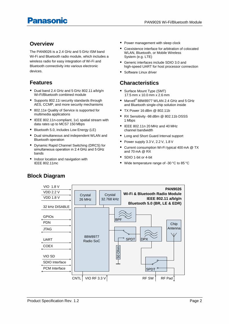
Chip
Antenna
SPDT
88W8977
Radio SoC
Crystal
32.768 kHz
SPI
UART
COEX
GPIOs
Status LED's
MCU Ready
PDN
Factory Reset
V SPDT
Wake Up's
JTAG
VIO 1.8 V
BPF
RF Pad
PAN9026
Wi-Fi & Bluetooth Radio Module
IEEE 802.11 a/b/g/n
Bluetooth 5.0 (BR, LE & EDR)
Crystal
26 MHz
DPXSPDT
50
Ohm
VDD 2.2 V
VDD 1.8 V
PCM Interface
SDIO Interface
VIO SD
32 kHz DISABLE
RF SWVIO RF 3.3 VCNTL
Overview
The PAN9026 is a 2.4 GHz and 5 GHz ISM band
Wi-Fi and Bluetooth radio module, which includes a
wireless radio for easy integration of Wi-Fi and
Bluetooth connectivity into various electronic
devices.
Features
• Dual band 2.4 GHz and 5 GHz 802.11 a/b/g/n Wi-Fi/Bluetooth combined module
• Supports 802.11i security standards through AES, CCMP, and more security mechanisms
• 802.11e Quality of Service is supported for multimedia applications
• IEEE 802.11n-compliant, 1x1 spatial stream with data rates up to MCS7 150 Mbps
• Bluetooth 5.0, includes Low Energy (LE)
• Dual simultaneous and independent WLAN and Bluetooth operation
• Dynamic Rapid Channel Switching (DRCS) for simultaneous operation in 2.4 GHz and 5 GHz bands
• Indoor location and navigation with IEEE 802.11mc
• Power management with sleep clock
• Coexistence interface for arbitration of colocated WLAN, Bluetooth, or Mobile Wireless System (e.g. LTE)
• Generic interfaces include SDIO 3.0 and high-speed UART for host processor connection
• Software Linux driver
Characteristics
• Surface Mount Type (SMT) 17.5 mm x 10.0 mm x 2.6 mm
• Marvell®
88W8977 WLAN 2.4 GHz and 5 GHz and Bluetooth single-chip solution inside
• TX Power 16 dBm @ 802.11b
• RX Sensitivity -98 dBm @ 802.11b DSSS 1 Mbps
• IEEE 802.11n 20 MHz and 40 MHz channel bandwidth
• Long and Short Guard Interval support
• Power supply 3.3 V, 2.2 V, 1.8 V
• Current consumption Wi-Fi typical 400 mA @ TX and 70 mA @ RX
• SDIO 1-bit or 4-bit
• Wide temperature range of -30 °C to 85 °C
Block Diagram
PAN9026 Wi-Fi/Bluetooth Module
Product Specification Rev. 1.2 Page 3
By purchase of any of the products described in this document the customer accepts the document's
validity and declares their agreement and understanding of its contents and recommendations. Panasonic
reserves the right to make changes as required at any time without notification. Please consult the most
recently issued Product Specification before initiating or completing a design.
© Panasonic Industrial Devices Europe GmbH 2019.
This specification sheet is copyrighted. Reproduction of this document is permissible only if reproduction is
without alteration and is accompanied by all associated warranties, conditions, limitations, and notices. Do
not disclose it to a third party.
All rights reserved.
This Product Description does not lodge the claim to be complete and free of mistakes.
Engineering Samples (ES)
If Engineering Samples are delivered to the customer, these samples have the status “Engineering
Samples”. This means that the design of this product is not yet concluded. Engineering Samples may be
partially or fully functional, and they may differ from the published Product Specification.
Engineering Samples are not qualified and they are not to be used for reliability testing or series
production.
Disclaimer
The customer acknowledges that samples may deviate from the Product Specification and may bear
defects due to their status of development and the lack of qualification mentioned above.
Panasonic rejects any liability or product warranty for Engineering Samples. In particular, Panasonic
disclaims liability for damages caused by:
The use of the Engineering Sample other than for evaluation purposes, particularly the installation
or integration in another product to be sold by the customer,
Deviation or lapse in function of the Engineering Sample,
Improper use of the Engineering Sample.
Panasonic Industrial Devices Europe GmbH disclaims any liability for consequential and incidental
damages. In case of any queries regarding the Engineering Samples, please contact your local sales
partner or the related product manager.
PAN9026 Wi-Fi/Bluetooth Module
Product Specification Rev. 1.2 Page 4
Table of Contents
1 About This Document ......................................................................................................................... 6
1.1 Purpose and Audience .............................................................................................................. 6
1.2 Revision History ......................................................................................................................... 6
1.3 Use of Symbols ......................................................................................................................... 7
1.4 Related Documents ................................................................................................................... 7
2 Overview .............................................................................................................................................. 8
2.1 Block Diagram ........................................................................................................................... 9
2.2 Pin Configuration ..................................................................................................................... 10
2.3 Power Management................................................................................................................. 15
2.4 Host Interfaces ........................................................................................................................ 16
2.5 Peripheral Bus Interface .......................................................................................................... 17
2.6 PCM Interface .......................................................................................................................... 17
2.7 Coexistence ............................................................................................................................. 18
2.8 WLAN ...................................................................................................................................... 29
2.9 Bluetooth ................................................................................................................................. 37
3 Detailed Description ......................................................................................................................... 39
3.1 Dimensions .............................................................................................................................. 39
3.2 Footprint .................................................................................................................................. 40
3.3 Packaging ................................................................................................................................ 41
3.4 Case Marking .......................................................................................................................... 44
4 Specification ..................................................................................................................................... 45
4.1 Default Test Conditions ........................................................................................................... 45
4.2 Absolute Maximum Ratings ..................................................................................................... 46
4.3 Recommended Operating Conditions ...................................................................................... 47
4.4 RF Electrical Characteristics .................................................................................................... 65
4.5 Reliability Tests ....................................................................................................................... 75
4.6 Recommended Soldering Profile ............................................................................................. 76
5 Cautions ............................................................................................................................................ 77
5.1 Design Notes ........................................................................................................................... 77
5.2 Installation Notes ..................................................................................................................... 77
5.3 Usage Condition Notes ............................................................................................................ 78
5.4 Storage Notes .......................................................................................................................... 78
5.5 Safety Cautions ....................................................................................................................... 79
5.6 Other Cautions ........................................................................................................................ 79
5.7 Restricted Use ......................................................................................................................... 80
6 Regulatory and Certification Information ....................................................................................... 81
6.1 Federal Communications Commission (FCC) for US .............................................................. 81
6.2 Innovation, Science, and Economic Development (ISED) for Canada .................................... 85
6.3 European Conformity According to RED (2014/53/EU) ........................................................... 94
6.4 Bluetooth Qualification ............................................................................................................. 97
6.5 RoHS And REACH Declaration ............................................................................................... 97
PAN9026 Wi-Fi/Bluetooth Module
Product Specification Rev. 1.2 Page 5
7 Appendix ........................................................................................................................................... 98
7.1 Ordering Information ................................................................................................................ 98
7.2 Contact Details ........................................................................................................................ 99
PAN9026 Wi-Fi/Bluetooth Module
1 About This Document
Product Specification Rev. 1.2 Page 6
1 About This Document
1.1 Purpose and Audience
This Product Specification provides details on the functional, operational, and electrical
characteristics of the Panasonic PAN9026 modules. It is intended for hardware design,
application, and Original Equipment Manufacturers (OEM) engineers. The product is referred to
as “the PAN9026” or “the module” within this document.
1.2 Revision History
Revision Date Modifications/Remarks
1.0 2017-12-20 Changed to Bluetooth 5.0.
Changed PM in chapter “Power Configuration Example with 3.3 V Host
Operation“.
Included values in chapter “Current Consumption“ and chapter ”RF
Characteristics“.
Removed chapter “TDM Interface”.
Additional models in chapter “Ordering Information”.
Added section in chapter “Acronyms and Abbreviations“.
1.1 2018-07-03 Renamed section in chapter “Restricted Use“.
Moved section in chapter “Life Support Policy”.
Added section in chapter “Restricted End Use“.
Added additional models “Ordering Information“.
1.2 2019-06-24 Changed Block Diagram in chapter “Power Configuration Example with 3.3 V
Host Operation“.
Added Table in chapter “Channel Tables based on Regulatory
Domain/Country“.
Changed Storage Temperature in chapter “Absolute Maximum Ratings“.
Changed Power-Up in chapter “Power-up Sequence“.
Restructure and update chapter “Cautions“.
Added section in chapter “Regulatory and Certification Information“.
Added additional models in chapter “Ordering Information“.
Formal and structure changes.
PAN9026 Wi-Fi/Bluetooth Module
1 About This Document
Product Specification Rev. 1.2 Page 7
1.3 Use of Symbols
Symbol Description
Note
Indicates important information for the proper use of the product.
Non-observance can lead to errors.
Attention
Indicates important notes that, if not observed, can put the product’s functionality
at risk.
[chapter number]
[chapter title]
Cross reference
Indicates cross references within the document.
Example:
Description of the symbols used in this document 1.3 Use of Symbols.
1.4 Related Documents
Please refer to the Panasonic website for related documents 7.2.2 Product Information.
PAN9026 Wi-Fi/Bluetooth Module
2 Overview
Product Specification Rev. 1.2 Page 8
2 Overview
The PAN9026 is a dual band 2.4 GHz and 5 GHz 802.11 a/b/g/n Wi-Fi radio module with
integrated Bluetooth BR/EDR/LE, specifically designed for highly integrated and cost-effective
applications. The simultaneous and independent operation of the two standards enables high
data rates (802.11n) and low-power operation (Bluetooth Low Energy). Integrated power
management, a fast dual-core CPU, 802.11i security standard support, and high-speed data
interfaces deliver the performance for the speed, reliability, and quality requirements of next
generation products. TX power calibration data and Wi-Fi/Bluetooth system parameters are
pre-stored on the one-time-programmable memory of the PAN9026 during production at
Panasonic. This simplifies passing the certification process for PAN9026 customers.
Furthermore, the module reduces design, test, and calibration effort resulting in reduced
time-to-market compared to discrete solutions.
Integrating Wi-Fi and Bluetooth wireless connectivity allows applications such as Smart Energy
and home gateways to manage multiple devices and appliances. The combination of Wi-Fi and
Bluetooth provides the highest flexibility for connectivity.
Please refer to the Panasonic website for related documents 7.2.2 Product Information.
Further information on the variants and versions 7.1 Ordering Information.
PAN9026 Wi-Fi/Bluetooth Module
2 Overview
Product Specification Rev. 1.2 Page 9
2.1 Block Diagram
Chip
Antenna
SPDT
88W8977
Radio SoC
Crystal
32.768 kHz
SPI
UART
COEX
GPIOs
Status LED's
MCU Ready
PDN
Factory Reset
V SPDT
Wake Up's
JTAG
VIO 1.8 V
BPF
RF Pad
PAN9026
Wi-Fi & Bluetooth Radio Module
IEEE 802.11 a/b/g/n
Bluetooth 5.0 (BR, LE & EDR)
Crystal
26 MHz
DPXSPDT5
0 O
hm
VDD 2.2 V
VDD 1.8 V
PCM Interface
SDIO Interface
VIO SD
32 kHz DISABLE
RF SWVIO RF 3.3 VCNTL
PAN9026 Wi-Fi/Bluetooth Module
2 Overview
Product Specification Rev. 1.2 Page 10
2.2 Pin Configuration
Pin Assignment
Pin Functions
No. Pin Name Pin Type Description
A1 1 PCM_DOUT Output signal PCM data output signal
IO5 Digital I/O General Purpose IO: GPIO[5]
A2 32KHZ_IN NC Do not connect
A3 PDN Input signal Power down (active-low) is derived from VDD1V8, can accept an
input signal of 1.8 V to 3.6 V (external pull-up resistor), it can be
driven by the host and must be high for normal operation.
A4 VDD1V8 Power 1.7 V to 1.9 V (typ. 1.8 V) power supply connection
A5 VDD1V8 Power 1.7 V to 1.9 V (typ. 1.8 V) power supply connection
A6 VDD2V2 Power 2.1 V to 2.3 V (typ. 2.2 V) power supply connection
A7 RF_SW1 Input signal RF Switch Pin 1: logical voltage level to activate on-board antenna or
RF Pad RF-Switch Pins Function
A8 GND Ground pin Connect to ground
A9 RF_OUT RF port 50 bottom pad to be activated by RF_SW1/RF_SW2 control
voltage RF-Switch Pins Function
1 Multi-purpose pins: After the firmware download, the pins (GPIO, Serial Interface, RF control) are programmed in functional mode with dedicated functionality.
A1
B1
C1
D1
E1
F1
A2
B2
C2
D2
E2
F2
G2
A3
B3
C3
D3
E3
F3
G3
A4
B4
C4
D4
E4
F4
G4
A5
B5
F5
G5
A6
B6
F6
G6
A7
B7
F7
G7
A8
B8
F8
G8
A9
B9
C9
D9
E9
F9
G9
EP1 EP2
Ch
ip
An
ten
na
10
,00
mm Ground plane
keep out area
Top View
G1
17,50 mm
PAN9026 Wi-Fi/Bluetooth Module
2 Overview
Product Specification Rev. 1.2 Page 11
No. Pin Name Pin Type Description
B1 1 PCM_CLK Input/output PCM clock signal, output if PCM master, input if PCM slave
IO6 Digital I/O General Purpose IO: GPIO[6]
B2 1 PCM_DIN Input signal PCM data input signal
IO4 Digital I/O General Purpose IO: GPIO[4]
B3 1 PCM_SYNC
2 Input/output PCM Sync Pulse signal, output if PCM master, input if PCM slave
IO7 3 Digital I/O General Purpose IO: GPIO[7]
B4 32KHZ_EN Input Signal If using VIO 3.3 V disable the internal 32.768 kHz crystal oscillator
(100 to GND) to use the SoC reference clock with lower accuracy
B5 VDD2V2 Power 2.1 V to 2.3 V (typ. 2.2 V) power supply connection
B6 VDD2V2 Power 2.1 V to 2.3 V (typ. 2.2 V) power supply connection
B7 RF_SW2 Input signal RF Switch Pin 2: logical voltage level to activate on-board antenna or
RF Pad RF-Switch Pins Function
B8 GND Ground pin Connect to ground
B9 GND Ground pin Connect to ground
C1 IO2 Digital I/O General Purpose IO: GPIO[2]
DVSC[0] Output signal Digital voltage scaling control for PMIC (VOUT 2.2 V)
2.3.1 Power Configuration Example with 3.3 V Host Operation
C2 IO3 Digital I/O General Purpose IO: GPIO[3]
DVSC[1] Output signal Digital voltage scaling control for PMIC (VOUT 1.05 V) (not used)
C3 IO1 Digital I/O General Purpose IO: GPIO[1]
C4 COEX_SIN Input signal Serial data input from MWS modem or peripheral device
C9 GND Ground pin Connect to ground
D1 IO15 Digital I/O General Purpose IO: GPIO[15]
D2 IO14 Digital I/O General Purpose IO: GPIO[14]
D3 DNC_E3 NC Do not connect
D4 COEX_SOUT Output signal Serial data output to MWS modem or peripheral device
D9 GND Ground pin Connect to ground
E1 SD_CLK Digital I/O For SDIO specific terminals SDIO Pins Function
E2 SD_CMD Digital I/O For SDIO specific terminals SDIO Pins Function
E3 IO0 Digital I/O General Purpose IO: GPIO[0]
E4 DNC_E4 NC Do not connect
2 PCM Mode: After enabling the mode by host command, the pin is used as PCM Audio Interface.
3 GPIO Mode: After enabling the mode by host command, the pin is used as Multi-Purpose Interface.
PAN9026 Wi-Fi/Bluetooth Module
2 Overview
Product Specification Rev. 1.2 Page 12
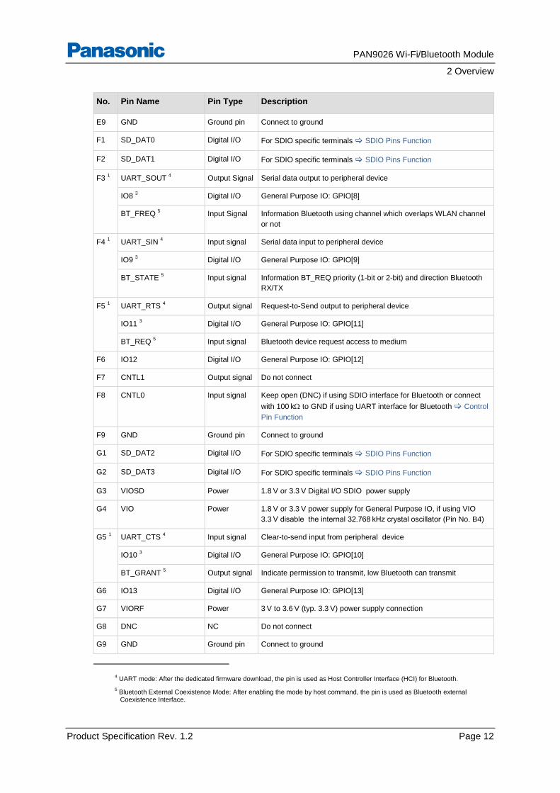
No. Pin Name Pin Type Description
E9 GND Ground pin Connect to ground
F1 SD_DAT0 Digital I/O For SDIO specific terminals SDIO Pins Function
F2 SD_DAT1 Digital I/O For SDIO specific terminals SDIO Pins Function
F3 1 UART_SOUT
4 Output Signal Serial data output to peripheral device
IO8 3 Digital I/O General Purpose IO: GPIO[8]
BT_FREQ 5 Input Signal Information Bluetooth using channel which overlaps WLAN channel
or not
F4 1 UART_SIN
4 Input signal Serial data input to peripheral device
IO9 3 Digital I/O General Purpose IO: GPIO[9]
BT_STATE 5 Input signal Information BT_REQ priority (1-bit or 2-bit) and direction Bluetooth
RX/TX
F5 1 UART_RTS
4 Output signal Request-to-Send output to peripheral device
IO11 3 Digital I/O General Purpose IO: GPIO[11]
BT_REQ 5 Input signal Bluetooth device request access to medium
F6 IO12 Digital I/O General Purpose IO: GPIO[12]
F7 CNTL1 Output signal Do not connect
F8 CNTL0 Input signal Keep open (DNC) if using SDIO interface for Bluetooth or connect
with 100 k to GND if using UART interface for Bluetooth Control
Pin Function
F9 GND Ground pin Connect to ground
G1 SD_DAT2 Digital I/O For SDIO specific terminals SDIO Pins Function
G2 SD_DAT3 Digital I/O For SDIO specific terminals SDIO Pins Function
G3 VIOSD Power 1.8 V or 3.3 V Digital I/O SDIO power supply
G4 VIO Power 1.8 V or 3.3 V power supply for General Purpose IO, if using VIO
3.3 V disable the internal 32.768 kHz crystal oscillator (Pin No. B4)
G5 1 UART_CTS
4 Input signal Clear-to-send input from peripheral device
IO10 3 Digital I/O General Purpose IO: GPIO[10]
BT_GRANT 5 Output signal Indicate permission to transmit, low Bluetooth can transmit
G6 IO13 Digital I/O General Purpose IO: GPIO[13]
G7 VIORF Power 3 V to 3.6 V (typ. 3.3 V) power supply connection
G8 DNC NC Do not connect
G9 GND Ground pin Connect to ground
4 UART mode: After the dedicated firmware download, the pin is used as Host Controller Interface (HCI) for Bluetooth.
5 Bluetooth External Coexistence Mode: After enabling the mode by host command, the pin is used as Bluetooth external Coexistence Interface.
PAN9026 Wi-Fi/Bluetooth Module
2 Overview
Product Specification Rev. 1.2 Page 13
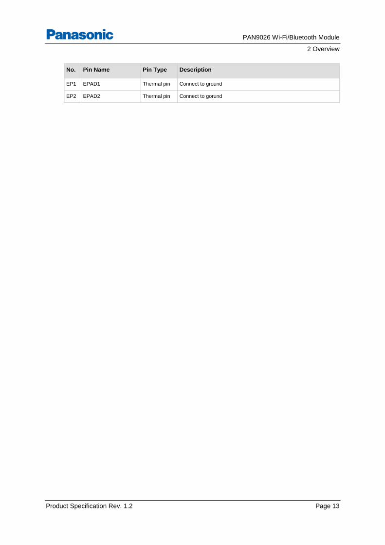
No. Pin Name Pin Type Description
EP1 EPAD1 Thermal pin Connect to ground
EP2 EPAD2 Thermal pin Connect to gorund
PAN9026 Wi-Fi/Bluetooth Module
2 Overview
Product Specification Rev. 1.2 Page 14
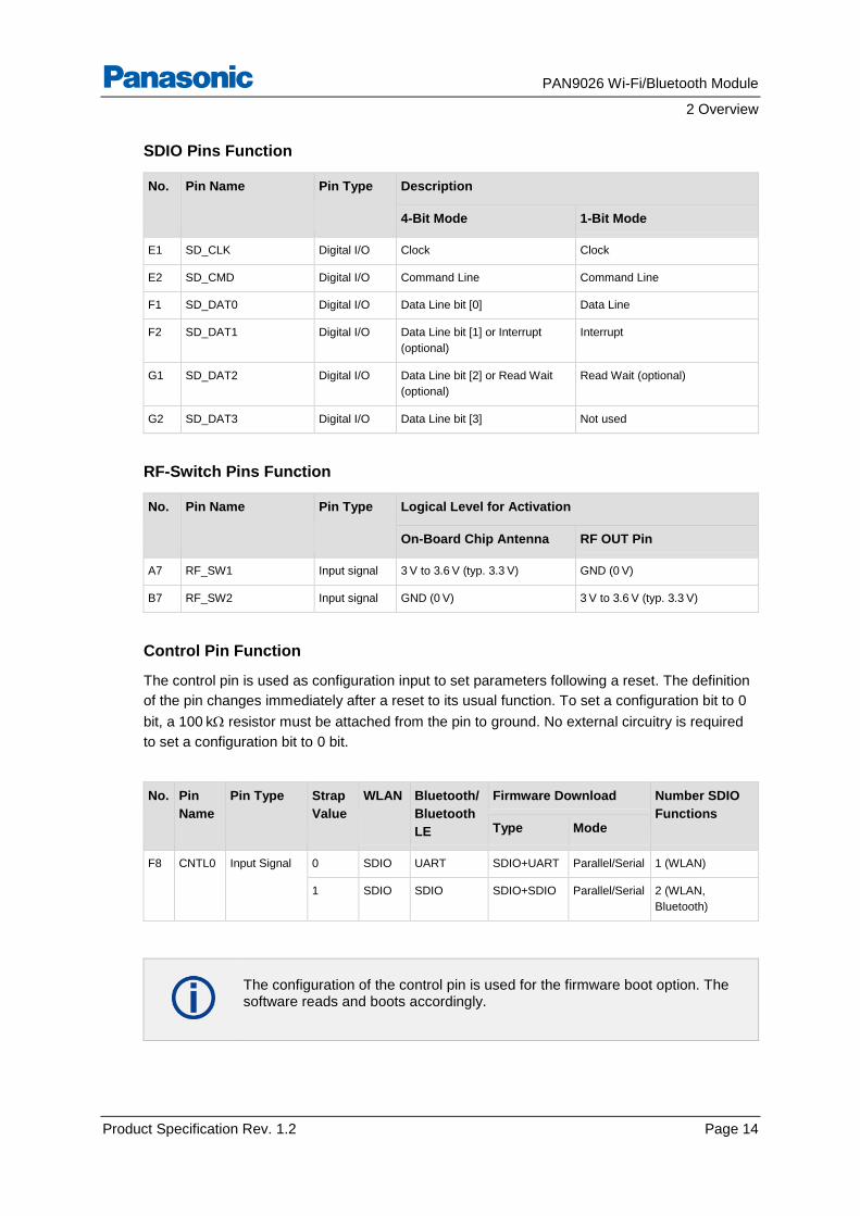
SDIO Pins Function
No. Pin Name Pin Type Description
4-Bit Mode 1-Bit Mode
E1 SD_CLK Digital I/O Clock Clock
E2 SD_CMD Digital I/O Command Line Command Line
F1 SD_DAT0 Digital I/O Data Line bit [0] Data Line
F2 SD_DAT1 Digital I/O Data Line bit [1] or Interrupt
(optional)
Interrupt
G1 SD_DAT2 Digital I/O Data Line bit [2] or Read Wait
(optional)
Read Wait (optional)
G2 SD_DAT3 Digital I/O Data Line bit [3] Not used
RF-Switch Pins Function
No. Pin Name Pin Type Logical Level for Activation
On-Board Chip Antenna RF OUT Pin
A7 RF_SW1 Input signal 3 V to 3.6 V (typ. 3.3 V) GND (0 V)
B7 RF_SW2 Input signal GND (0 V) 3 V to 3.6 V (typ. 3.3 V)
Control Pin Function
The control pin is used as configuration input to set parameters following a reset. The definition
of the pin changes immediately after a reset to its usual function. To set a configuration bit to 0
bit, a 100 k resistor must be attached from the pin to ground. No external circuitry is required
to set a configuration bit to 0 bit.
No. Pin
Name
Pin Type Strap
Value
WLAN Bluetooth/
Bluetooth
LE
Firmware Download Number SDIO
Functions Type Mode
F8 CNTL0 Input Signal 0 SDIO UART SDIO+UART Parallel/Serial 1 (WLAN)
1 SDIO SDIO SDIO+SDIO Parallel/Serial 2 (WLAN,
Bluetooth)
The configuration of the control pin is used for the firmware boot option. The software reads and boots accordingly.
PAN9026 Wi-Fi/Bluetooth Module
2 Overview
Product Specification Rev. 1.2 Page 15
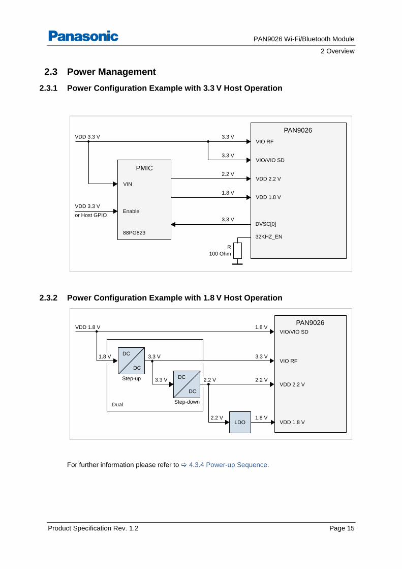
2.3 Power Management
2.3.1 Power Configuration Example with 3.3 V Host Operation
2.3.2 Power Configuration Example with 1.8 V Host Operation
For further information please refer to 4.3.4 Power-up Sequence.
PAN9026
VIO/VIO SD
VIO RF
VDD 2.2 V
VDD 1.8 V
DVSC[0]
88PG823
PMIC
Enable
VDD 3.3 V 3.3 V
3.3 V
2.2 V
1.8 V
3.3 V
VDD 3.3 V
or Host GPIO
VIN
R
100 Ohm
32KHZ_EN
PAN9026
VIO/VIO SD
VIO RF
VDD 2.2 V
VDD 1.8 V
3.3 V
2.2 V
1.8 V
DC
DC
DC
DC
LDO
Step-up
Step-down
VDD 1.8 V 1.8 V
1.8 V
3.3 V
3.3 V
2.2 V
2.2 V
Dual
PAN9026 Wi-Fi/Bluetooth Module
2 Overview
Product Specification Rev. 1.2 Page 16
2.4 Host Interfaces
The bus interface connects several host interface bus units to the CPU bus of the device
through the internal bus. The connection of each unit is multiplexed with other bus units.
The high-speed UART interface is connected to the CPU bus through a separate bus.
Type Features
High-speed UART interface The device supports a high-speed Universal Asynchronous
Receiver/Transmitter (UART) interface, compliant with the industry
standard 16550 specification.
• FIFO mode permanently selected for transmit and receive operations
• Two pins for transmit and receive operations
• Two flow control pins
• Interrupt triggers for low-power, high throughput operation
SDIO interface The device supports an SDIO device interface that conforms to the
industry standard SDIO full-speed card specification and allows a host
controller using the SDIO bus protocol to access the device.
• Supports SDIO 3.0 Standard
• 1-bit SDIO or 4-bit SDIO transfer modes with full clock range up to 100 MHz
• On-chip memory used for CIS
• Special interrupt register for information exchange
• Allows card to interrupt host
For further information please refer to 4.3.5 Host Interface.
PAN9026 Wi-Fi/Bluetooth Module
2 Overview
Product Specification Rev. 1.2 Page 17
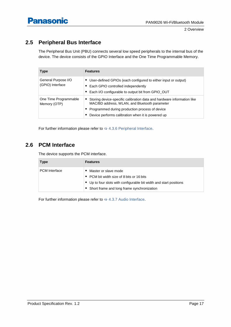
2.5 Peripheral Bus Interface
The Peripheral Bus Unit (PBU) connects several low speed peripherals to the internal bus of the
device. The device consists of the GPIO Interface and the One Time Programmable Memory.
Type Features
General Purpose I/O
(GPIO) Interface
• User-defined GPIOs (each configured to either input or output)
• Each GPIO controlled independently
• Each I/O configurable to output bit from GPIO_OUT
One Time Programmable
Memory (OTP)
• Storing device-specific calibration data and hardware information like MAC/BD address, WLAN, and Bluetooth parameter
• Programmed during production process of device
• Device performs calibration when it is powered up
For further information please refer to 4.3.6 Peripheral Interface.
2.6 PCM Interface
The device supports the PCM interface.
Type Features
PCM Interface • Master or slave mode
• PCM bit width size of 8 bits or 16 bits
• Up to four slots with configurable bit width and start positions
• Short frame and long frame synchronization
For further information please refer to 4.3.7 Audio Interface.
PAN9026 Wi-Fi/Bluetooth Module
2 Overview
Product Specification Rev. 1.2 Page 18
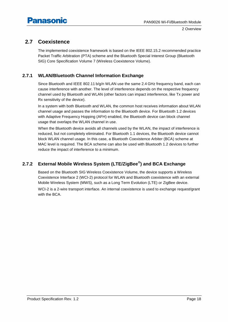
2.7 Coexistence
The implemented coexistence framework is based on the IEEE 802.15.2 recommended practice
Packet Traffic Arbitration (PTA) scheme and the Bluetooth Special Interest Group (Bluetooth
SIG) Core Specification Volume 7 (Wireless Coexistence Volume).
2.7.1 WLAN/Bluetooth Channel Information Exchange
Since Bluetooth and IEEE 802.11 b/g/n WLAN use the same 2.4 GHz frequency band, each can
cause interference with another. The level of interference depends on the respective frequency
channel used by Bluetooth and WLAN (other factors can impact interference, like Tx power and
Rx sensitivity of the device).
In a system with both Bluetooth and WLAN, the common host receives information about WLAN
channel usage and passes the information to the Bluetooth device. For Bluetooth 1.2 devices
with Adaptive Frequency Hopping (AFH) enabled, the Bluetooth device can block channel
usage that overlaps the WLAN channel in use.
When the Bluetooth device avoids all channels used by the WLAN, the impact of interference is
reduced, but not completely eliminated. For Bluetooth 1.1 devices, the Bluetooth device cannot
block WLAN channel usage. In this case, a Bluetooth Coexistence Arbiter (BCA) scheme at
MAC level is required. The BCA scheme can also be used with Bluetooth 1.2 devices to further
reduce the impact of interference to a minimum.
2.7.2 External Mobile Wireless System (LTE/ZigBee®) and BCA Exchange
Based on the Bluetooth SIG Wireless Coexistence Volume, the device supports a Wireless
Coexistence Interface 2 (WCI-2) protocol for WLAN and Bluetooth coexistence with an external
Mobile Wireless System (MWS), such as a Long Term Evolution (LTE) or ZigBee device.
WCI-2 is a 2-wire transport interface. An internal coexistence is used to exchange request/grant
with the BCA.
PAN9026 Wi-Fi/Bluetooth Module
2 Overview
Product Specification Rev. 1.2 Page 19
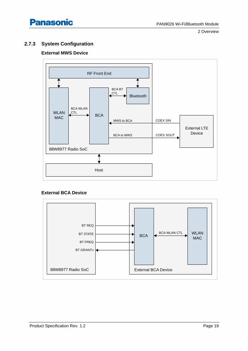
2.7.3 System Configuration
External MWS Device
External BCA Device
WLAN
MACBCA
Bluetooth
RF Front End
Host
BCA WLAN
CTL
BCA BT
CTL
MWS to BCA
BCA to MWS
COEX SIN
COEX SOUT
External LTE
Device
88W8977 Radio SoC
BCA WLAN CTL
External BCA Device
BCAWLAN
MAC
88W8977 Radio SoC
BT REQ
BT STATE
BT FREQ
BT GRANTn
PAN9026 Wi-Fi/Bluetooth Module
2 Overview
Product Specification Rev. 1.2 Page 20
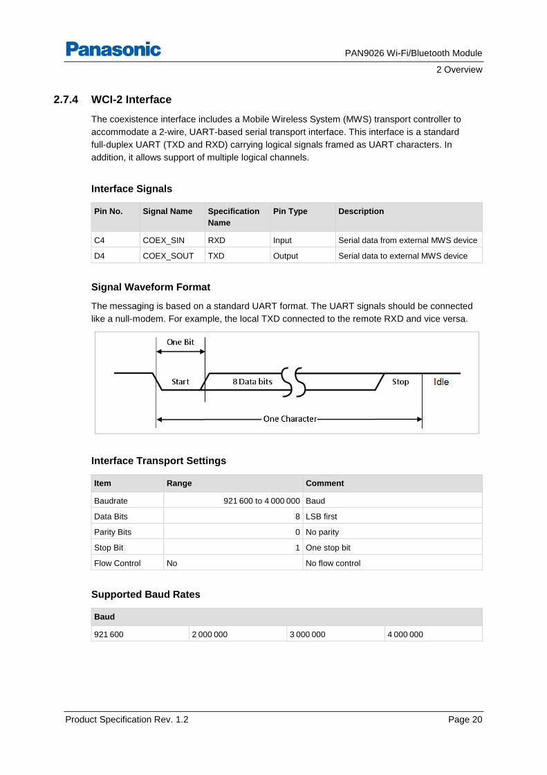
2.7.4 WCI-2 Interface
The coexistence interface includes a Mobile Wireless System (MWS) transport controller to
accommodate a 2-wire, UART-based serial transport interface. This interface is a standard
full-duplex UART (TXD and RXD) carrying logical signals framed as UART characters. In
addition, it allows support of multiple logical channels.
Interface Signals
Pin No. Signal Name Specification
Name
Pin Type Description
C4 COEX_SIN RXD Input Serial data from external MWS device
D4 COEX_SOUT TXD Output Serial data to external MWS device
Signal Waveform Format
The messaging is based on a standard UART format. The UART signals should be connected
like a null-modem. For example, the local TXD connected to the remote RXD and vice versa.
Interface Transport Settings
Item Range Comment
Baudrate 921 600 to 4 000 000 Baud
Data Bits 8 LSB first
Parity Bits 0 No parity
Stop Bit 1 One stop bit
Flow Control No No flow control
Supported Baud Rates
Baud
921 600 2 000 000 3 000 000 4 000 000
PAN9026 Wi-Fi/Bluetooth Module
2 Overview
Product Specification Rev. 1.2 Page 21
Real-Time Signaling Message
The real-time signaling message is used to transport real-time signals over the 2-wire transport
interface.
The real-time signaling message conveys the real-time signals (Bluetooth Core Specification,
Volume 7, Part A) in one message. The time reference point for the real-time signaling message
is the end of message bit 5 (transition to stop bit).
Defined real-time signaling messages include:
• Coexistence Controller to MWS device
• MWS device to Coexistence Controller
Real-Time Signaling MSG[0] MSG[1] MSG[2] MSG[3] MSG[4]
MWS to Coexistence
Controller (Signal)
FRAME_SYNC MWS_RX MWS_TX PATTERN[0] PATTERN[1]
Coexistence Controller to
MWS (Message)
BT_RX_PRI BT_TX_ON 802_RX_PRI 802_TX_ON RFU
Signal Name
FRAME_SYNC
MWS_RX
MWS_TX
PATTERN[1,0]
BT_RX_PRI
BT_TX_ON
802_RX_PRI
802_TX_ON
MWS_INACTIVITY_DURATION
MWS_SCAN_FREQUENCY_OFFSET
PAN9026 Wi-Fi/Bluetooth Module
2 Overview
Product Specification Rev. 1.2 Page 22
Transport Control Message
The transport control messages can modify the state and request state information of the MWS
coexistence interface.
Message MSG[0] MSG[1] MSG[2] MSG[3] MSG[4]
Transport Control Message RESEND_REA
L_TIME
RFU RFU RFU RFU
Signal Name Description
RESEND_REAL_TIME This bit is set if a device wants to get a status update of the real-time signals.
The signal is usually used after wake-up from sleep of the transport interface
to get an update of the real-time signals.
If the receiving device’s transport interface is awake it shall send a real-time
message with the current status of the real-time signals within four UART
character period. If the signal is not transmitted within four UART character
periods, the device is considered asleep.
If the receiving device’s transport interface is not awake it shall not send a
real-time message.
Bluetooth initiated:
If the MWS is currently scanning or has an ongoing inactivity duration, the
MWS shall send a frequency scan message or an inactivity duration message
after transmitting the real-time message.
If the receiving device’s transport interface is not awake it shall not send a
frequency scan or inactivity duration message.
Transparent Data Message
The transport control messages can modify the state and request state information of the MWS
coexistence interface.
Message MSG[0] MSG[1] MSG[2] MSG[3] MSG[4]
Transparent Data
Message
NIBBLE_POS
ITION
DATA[0]/
DATA[4]
DATA[1]/
DATA[5]
DATA[2]/
DATA[6]
DATA[3]/
DATA[7]
Signal Name Description
NIBBLE_POSITION 0 = least significant nibble
1 = most significant nibble
DATA[n]; n=0 … 7 Data bits of the message octet
PAN9026 Wi-Fi/Bluetooth Module
2 Overview
Product Specification Rev. 1.2 Page 23
MWS Inactivity Duration Message
The inactivity duration messages is used to send the signal MWS_INACTIVITY_DURATION
from the MWS device to the Coexistence Controller.
Message MSG[0] MSG[1] MSG[2] MSG[3] MSG[4]
MWS Inactivity Duration
Message
DURATION[0] DURATION[1] DURATION[2] DURATION[3] DURATION[4]
The idle duration is encoded in 5 bits given by the formula:
Inactivity_Duration = DURATION * 5 ms
Inactivity durarations smaller than 5 ms are not communicated.
If all bits are set to 1 the inactivity duration is infinite. If all bits are set to 0, signal MWS_RX, or
signal MWS_TX are set to 1, the inactivity period ends.
MWS Scan Frequency Offset Message
The MWS scan frequency offset message is used to send the signal
MWS_SCAN_FREQUENCY_ OFFSET from the MWS device to the Coexistence Controller.
Message MSG[0] MSG[1] MSG[2] MSG[3] MSG[4]
MWS Scan Frequency
Offset
BAND FREQ[0] FREQ [1] FREQ [2] FREQ [3]
The RF scan frequency is encoded in 5 bits given by the formula:
RF_FREQ_OFFSET = FREQ * 10 MHz
If BAND is set to o the signal RF_FREQ_OFFSET is the negative value from the lower edge of
the ISM band. If BAND is set to 1, signal RF_FREQ_OFFSET is the positive value from the top
edge of the ISM band.
FREQ set to all 0 indicates the end of the scan period.
PAN9026 Wi-Fi/Bluetooth Module
2 Overview
Product Specification Rev. 1.2 Page 24
2.7.5 Bluetooth Coexistence Arbiter
Type Features
Capability • Programmable coexistence interface timing, interface modes, and signal polarity to support a variety of external Bluetooth devices
• Programmable decision policies and transaction lock behavior for various use cases
• Interface with external or on-chip Bluetooth device
• Supports Bluetooth 1.1 or Bluetooth 1.2 AFH
• WLAN-coordinated/Bluetooth-coordinated low-power design
• Enhanced information sharing between WLAN and Bluetooth for combined systems
• WLAN/Bluetooth/MWS (LTE/ZigBee) coexistence support
Arbitration • Contention resolved by a customizable decision matrix that allows independent grant decision for each device
• Vectors for the decision matrix:
WLAN priority (2-bit)
WLAN direction
Bluetooth priority (1-bit or 2-bit)
Bluetooth direction
Bluetooth frequency in/out band
MWS priority (2-bit)
MWS direction
AFH If AFH is enabled in the Bluetooth device, and there is a sufficient
guard-band outside the WLAN operating frequency, the Bluetooth device
uses the Out-Of-Band (OOB) channel with respect to the WLAN device.
Otherwise, the Bluetooth device uses the In-Band (IB) and OOB channels
with respect to the WLAN device.
The IB and OOB information is either provided by the Bluetooth device
through the coexistence interface, or it can be provided through firmware
controls in a shared-host system. IB/OOB is a vector in the decision matrix.
PAN9026 Wi-Fi/Bluetooth Module
2 Overview
Product Specification Rev. 1.2 Page 25
Type Features
Decision Policies System configuration is a major consideration when planning decision
policies. The configuration governs how RF paths are shared and how
much interference will occur. Interference combinations include:
WLAN TX and Bluetooth TX
WLAN TX and Bluetooth RX
WLAN RX and Bluetooth TX
WLAN RX and Bluetooth RX
Interference combinations where WLAN and Bluetooth share the same
antenna:
WLAN TX and Bluetooth TX share the same antenna, the decision matrix allows either WLAN or Bluetooth TX (both OOB and IB), based on relative packet priorities.
WLAN TX and Bluetooth RX (both OOB and IB) have sizable interference impacts on Bluetooth RX, the decision matrix grants or denies WLAN TX based on relative packet priorities.
WLAN RX and Bluetooth TX (both OOB and IB) have sizable interference impacts on WLAN RX, the decision matrix grants or denies Bluetooth TX based on relative packet priorities.
WLAN RX and Bluetooth RX (both OOB and IB) have no impact on each other, the decision matrix grants both.
Interference combinations where WLAN and Bluetooth have their own
antenna:
WLAN TX and Bluetooth TX in OOB situation have little interference impact on each other, the decision matrix grants both.
WLAN TX and Bluetooth TX in IB have sizable interference impact on each other, the decision matrix allows either WLAN or Bluetooth TX, based on relative packet priorities.
WLAN TX and Bluetooth RX in OOB situation have little interference impact on each other, the decision matrix grants both provided there is enough antenna isolation between WLAN and Bluetooth antenna.
WLAN TX and Bluetooth RX in IB situation have sizable interference impact on Bluetooth RX, the decision matrix grants or denies WLAN TX based on relative packet priorities.
WLAN RX and Bluetooth TX in OOB situation have little interference impact on each other, the decision matrix grants both provided there is enough antenna isolation between WLAN and Bluetooth antenna.
WLAN RX and Bluetooth TX in IB situation have sizable interference impact on WLAN RX, the decision matrix grants or denies Bluetooth TX based on relative packet priorities.
WLAN RX and Bluetooth RX (both OOB and IB) have no impact on each other, the decision matrix grants both.
For the devices running in a basic shared antenna configuration, the linear
switching imposes restrictions on simultaneous transfer. Reasonable
policies include:
WLAN and Bluetooth are never granted at the same time
Decision matrix grants a device based on relative packet priorities and direction
Priority order: High > Medium High > Medium > Low
For equal priority contention, select one device to win, that optimizes the usage case
For the devices running in an enhanced shared antenna configuration, the
linear switching imposes restrictions on some simultaneous transfers.
PAN9026 Wi-Fi/Bluetooth Module
2 Overview
Product Specification Rev. 1.2 Page 26
Type Features
Transaction Stopping The arbiter allows control of what transfers can be stopped after an initial
grant. If allowed, a transaction can be stopped for higher priority request.
A transaction stop decision is a function of the decision policies and
transaction stopping control. The transaction stopping control is
configurable per device and direction.
2.7.6 Bluetooth Capability
Type Features
Request Schemes The PTA signals are directly controlled by the hardware to meet timing
requirements of the Bluetooth radio. The software controls the type of traffic
in priority mode. Mechanism enforced for control include:
• Selection of certain types of communication always treated as high priority
• Selection of individual frames marked with high priority
• Real-time signaling of the next slot marked with high priority
• Automatic hardware control, based on the grant/denial history of the Bluetooth link
Timing Control The signal timing scheme PTA is fully programmable relative to the
Bluetooth packet timing.
2.7.7 WLAN Capability
Type Features
Capability The WLAN device technology uses an internal coexistence interface to
exchange request/grant with the BCA.
• Packet-based request signaling with direction and priority information
• 1-bit or 2-bit priority signaling to support four priority levels
• Multiple WLAN RX request trigger sources, including early prediction
• WLAN TX request cancellation and abort if grant denied or revoked in middle of request
• 802.11n A-MPDU treated as single packet
Packet Classification • Programmable mask allows each frame type to be mapped to a priority
• Default setting puts response frames (ACK), beacons, and QoS frames as high priority
• WLAN TX and RX have separate priority mask
Queue Classification • Programmable mask allows each transmit queue to be mapped to a priority
• Queue-based mapping is optional for software-generated frames only
PAN9026 Wi-Fi/Bluetooth Module
2 Overview
Product Specification Rev. 1.2 Page 27
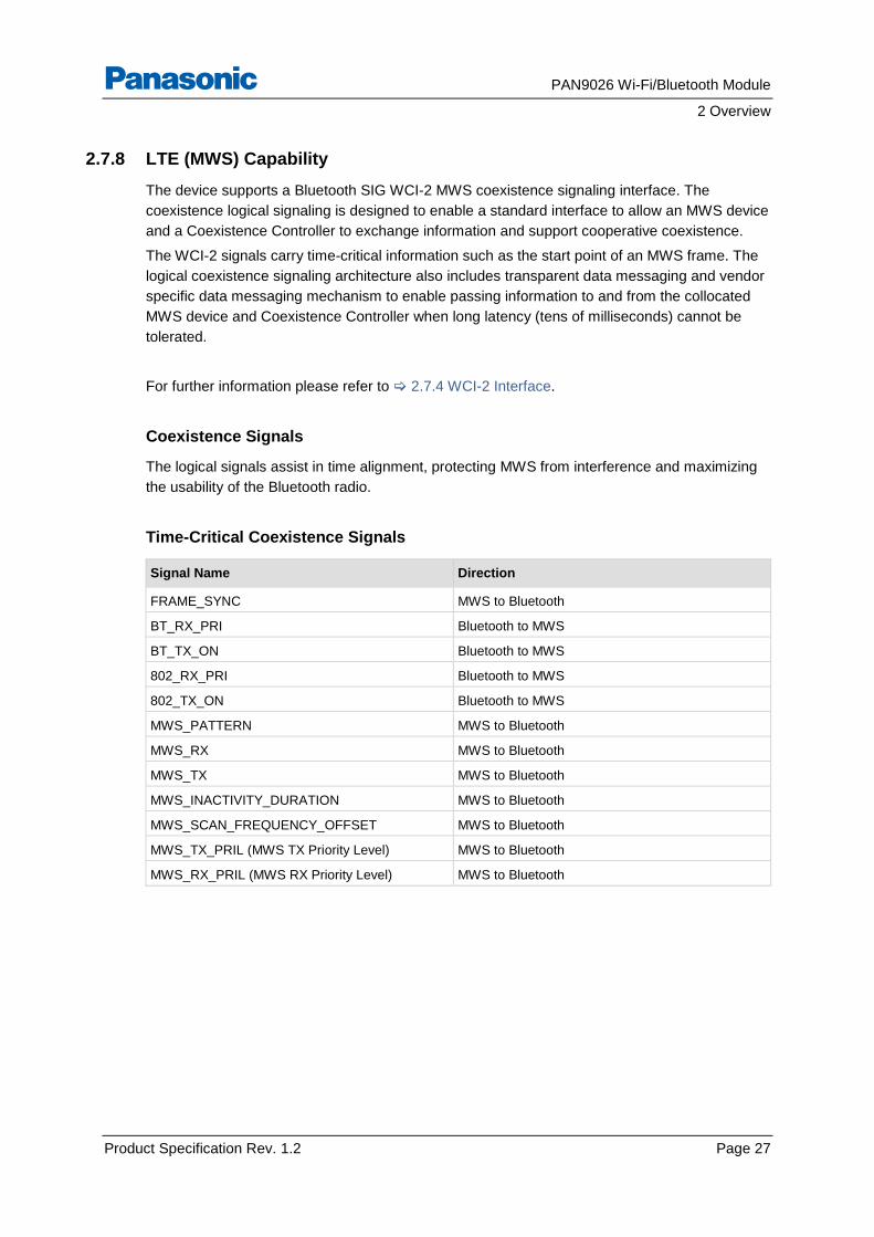
2.7.8 LTE (MWS) Capability
The device supports a Bluetooth SIG WCI-2 MWS coexistence signaling interface. The
coexistence logical signaling is designed to enable a standard interface to allow an MWS device
and a Coexistence Controller to exchange information and support cooperative coexistence.
The WCI-2 signals carry time-critical information such as the start point of an MWS frame. The
logical coexistence signaling architecture also includes transparent data messaging and vendor
specific data messaging mechanism to enable passing information to and from the collocated
MWS device and Coexistence Controller when long latency (tens of milliseconds) cannot be
tolerated.
For further information please refer to 2.7.4 WCI-2 Interface.
Coexistence Signals
The logical signals assist in time alignment, protecting MWS from interference and maximizing
the usability of the Bluetooth radio.
Time-Critical Coexistence Signals
Signal Name Direction
FRAME_SYNC MWS to Bluetooth
BT_RX_PRI Bluetooth to MWS
BT_TX_ON Bluetooth to MWS
802_RX_PRI Bluetooth to MWS
802_TX_ON Bluetooth to MWS
MWS_PATTERN MWS to Bluetooth
MWS_RX MWS to Bluetooth
MWS_TX MWS to Bluetooth
MWS_INACTIVITY_DURATION MWS to Bluetooth
MWS_SCAN_FREQUENCY_OFFSET MWS to Bluetooth
MWS_TX_PRIL (MWS TX Priority Level) MWS to Bluetooth
MWS_RX_PRIL (MWS RX Priority Level) MWS to Bluetooth
PAN9026 Wi-Fi/Bluetooth Module
2 Overview
Product Specification Rev. 1.2 Page 28
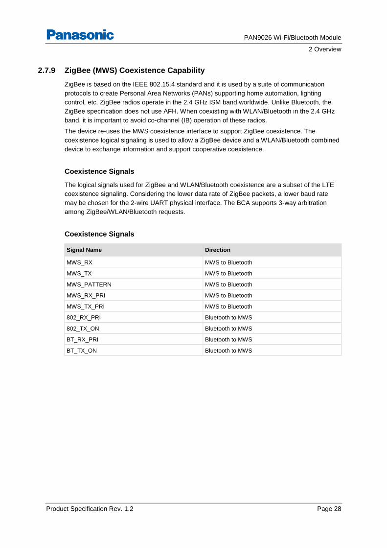
2.7.9 ZigBee (MWS) Coexistence Capability
ZigBee is based on the IEEE 802.15.4 standard and it is used by a suite of communication
protocols to create Personal Area Networks (PANs) supporting home automation, lighting
control, etc. ZigBee radios operate in the 2.4 GHz ISM band worldwide. Unlike Bluetooth, the
ZigBee specification does not use AFH. When coexisting with WLAN/Bluetooth in the 2.4 GHz
band, it is important to avoid co-channel (IB) operation of these radios.
The device re-uses the MWS coexistence interface to support ZigBee coexistence. The
coexistence logical signaling is used to allow a ZigBee device and a WLAN/Bluetooth combined
device to exchange information and support cooperative coexistence.
Coexistence Signals
The logical signals used for ZigBee and WLAN/Bluetooth coexistence are a subset of the LTE
coexistence signaling. Considering the lower data rate of ZigBee packets, a lower baud rate
may be chosen for the 2-wire UART physical interface. The BCA supports 3-way arbitration
among ZigBee/WLAN/Bluetooth requests.
Coexistence Signals
Signal Name Direction
MWS_RX MWS to Bluetooth
MWS_TX MWS to Bluetooth
MWS_PATTERN MWS to Bluetooth
MWS_RX_PRI MWS to Bluetooth
MWS_TX_PRI MWS to Bluetooth
802_RX_PRI Bluetooth to MWS
802_TX_ON Bluetooth to MWS
BT_RX_PRI Bluetooth to MWS
BT_TX_ON Bluetooth to MWS
PAN9026 Wi-Fi/Bluetooth Module
2 Overview
Product Specification Rev. 1.2 Page 29
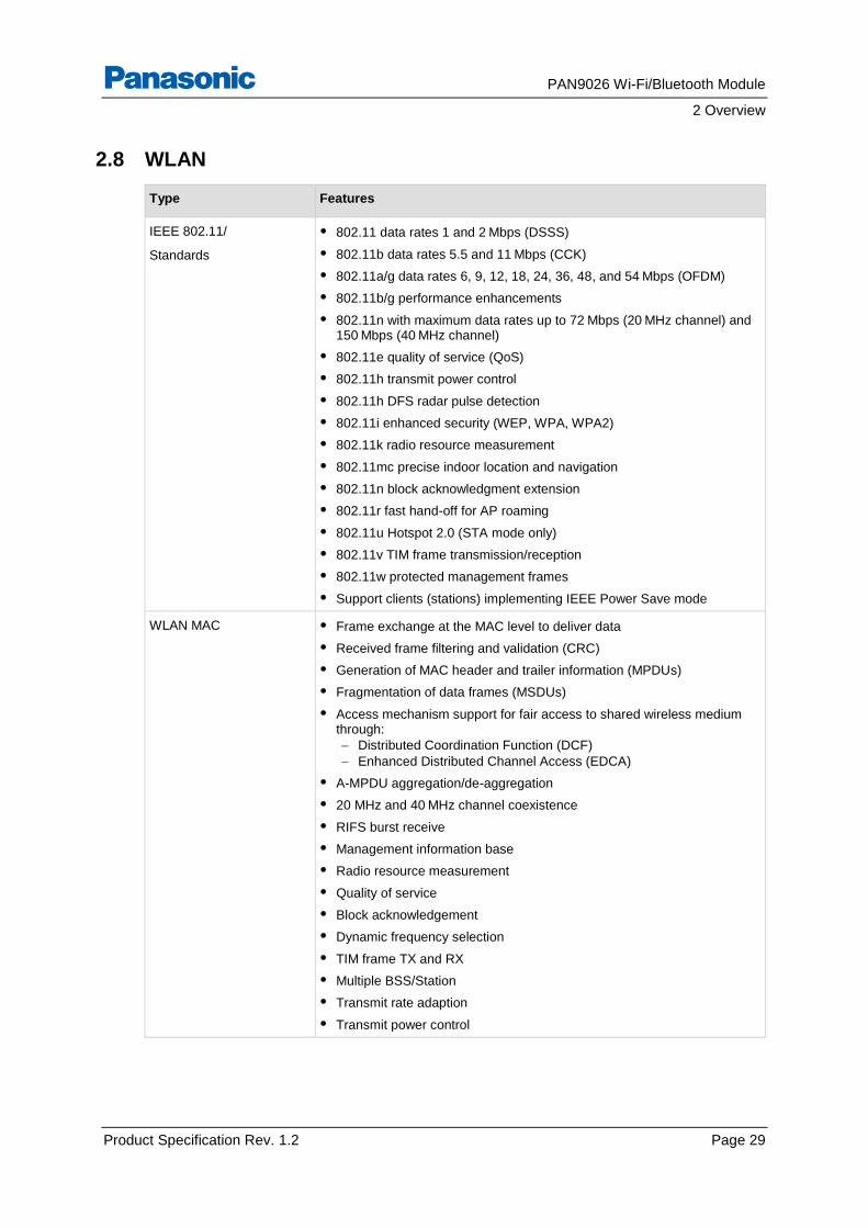
2.8 WLAN
Type Features
IEEE 802.11/
Standards
• 802.11 data rates 1 and 2 Mbps (DSSS)
• 802.11b data rates 5.5 and 11 Mbps (CCK)
• 802.11a/g data rates 6, 9, 12, 18, 24, 36, 48, and 54 Mbps (OFDM)
• 802.11b/g performance enhancements
• 802.11n with maximum data rates up to 72 Mbps (20 MHz channel) and 150 Mbps (40 MHz channel)
• 802.11e quality of service (QoS)
• 802.11h transmit power control
• 802.11h DFS radar pulse detection
• 802.11i enhanced security (WEP, WPA, WPA2)
• 802.11k radio resource measurement
• 802.11mc precise indoor location and navigation
• 802.11n block acknowledgment extension
• 802.11r fast hand-off for AP roaming
• 802.11u Hotspot 2.0 (STA mode only)
• 802.11v TIM frame transmission/reception
• 802.11w protected management frames
• Support clients (stations) implementing IEEE Power Save mode
WLAN MAC • Frame exchange at the MAC level to deliver data
• Received frame filtering and validation (CRC)
• Generation of MAC header and trailer information (MPDUs)
• Fragmentation of data frames (MSDUs)
• Access mechanism support for fair access to shared wireless medium through:
Distributed Coordination Function (DCF)
Enhanced Distributed Channel Access (EDCA)
• A-MPDU aggregation/de-aggregation
• 20 MHz and 40 MHz channel coexistence
• RIFS burst receive
• Management information base
• Radio resource measurement
• Quality of service
• Block acknowledgement
• Dynamic frequency selection
• TIM frame TX and RX
• Multiple BSS/Station
• Transmit rate adaption
• Transmit power control
PAN9026 Wi-Fi/Bluetooth Module
2 Overview
Product Specification Rev. 1.2 Page 30
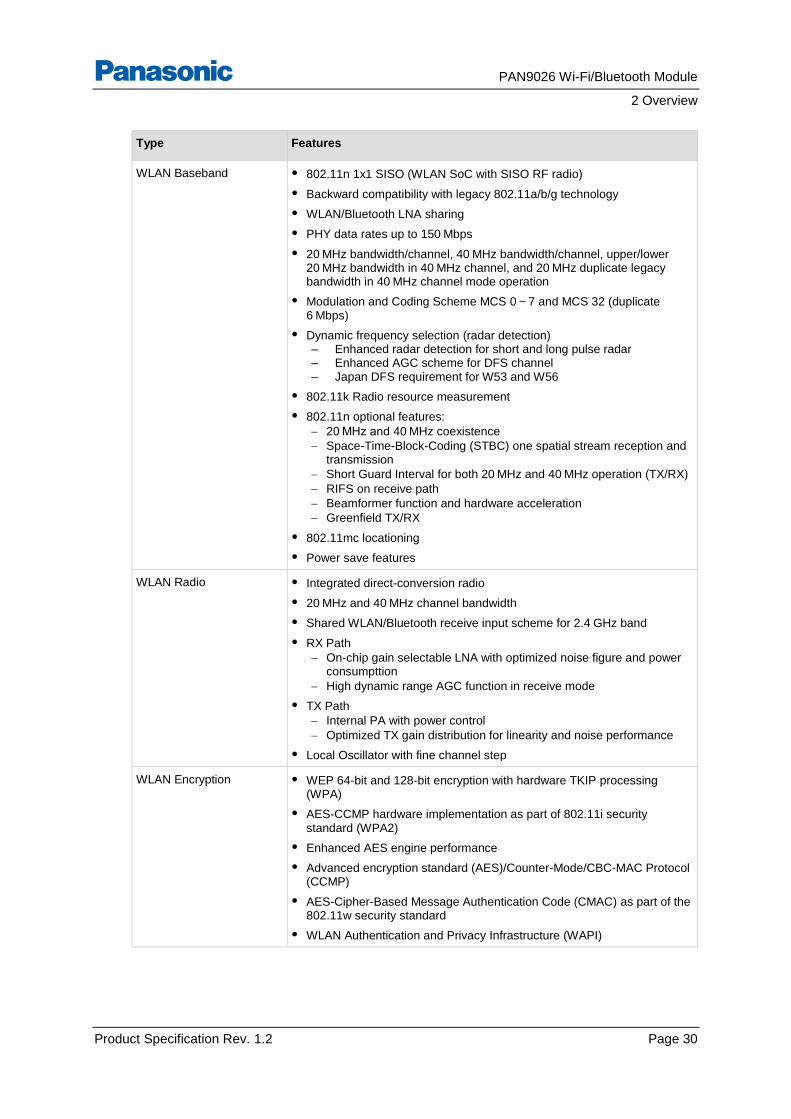
Type Features
WLAN Baseband • 802.11n 1x1 SISO (WLAN SoC with SISO RF radio)
• Backward compatibility with legacy 802.11a/b/g technology
• WLAN/Bluetooth LNA sharing
• PHY data rates up to 150 Mbps
• 20 MHz bandwidth/channel, 40 MHz bandwidth/channel, upper/lower 20 MHz bandwidth in 40 MHz channel, and 20 MHz duplicate legacy bandwidth in 40 MHz channel mode operation
• Modulation and Coding Scheme MCS 0 ~ 7 and MCS 32 (duplicate 6 Mbps)
• Dynamic frequency selection (radar detection) – Enhanced radar detection for short and long pulse radar – Enhanced AGC scheme for DFS channel – Japan DFS requirement for W53 and W56
• 802.11k Radio resource measurement
• 802.11n optional features:
20 MHz and 40 MHz coexistence
Space-Time-Block-Coding (STBC) one spatial stream reception and transmission
Short Guard Interval for both 20 MHz and 40 MHz operation (TX/RX)
RIFS on receive path
Beamformer function and hardware acceleration
Greenfield TX/RX
• 802.11mc locationing
• Power save features
WLAN Radio • Integrated direct-conversion radio
• 20 MHz and 40 MHz channel bandwidth
• Shared WLAN/Bluetooth receive input scheme for 2.4 GHz band
• RX Path
On-chip gain selectable LNA with optimized noise figure and power consumpttion
High dynamic range AGC function in receive mode
• TX Path
Internal PA with power control
Optimized TX gain distribution for linearity and noise performance
• Local Oscillator with fine channel step
WLAN Encryption • WEP 64-bit and 128-bit encryption with hardware TKIP processing (WPA)
• AES-CCMP hardware implementation as part of 802.11i security standard (WPA2)
• Enhanced AES engine performance
• Advanced encryption standard (AES)/Counter-Mode/CBC-MAC Protocol (CCMP)
• AES-Cipher-Based Message Authentication Code (CMAC) as part of the 802.11w security standard
• WLAN Authentication and Privacy Infrastructure (WAPI)
PAN9026 Wi-Fi/Bluetooth Module
2 Overview
Product Specification Rev. 1.2 Page 31
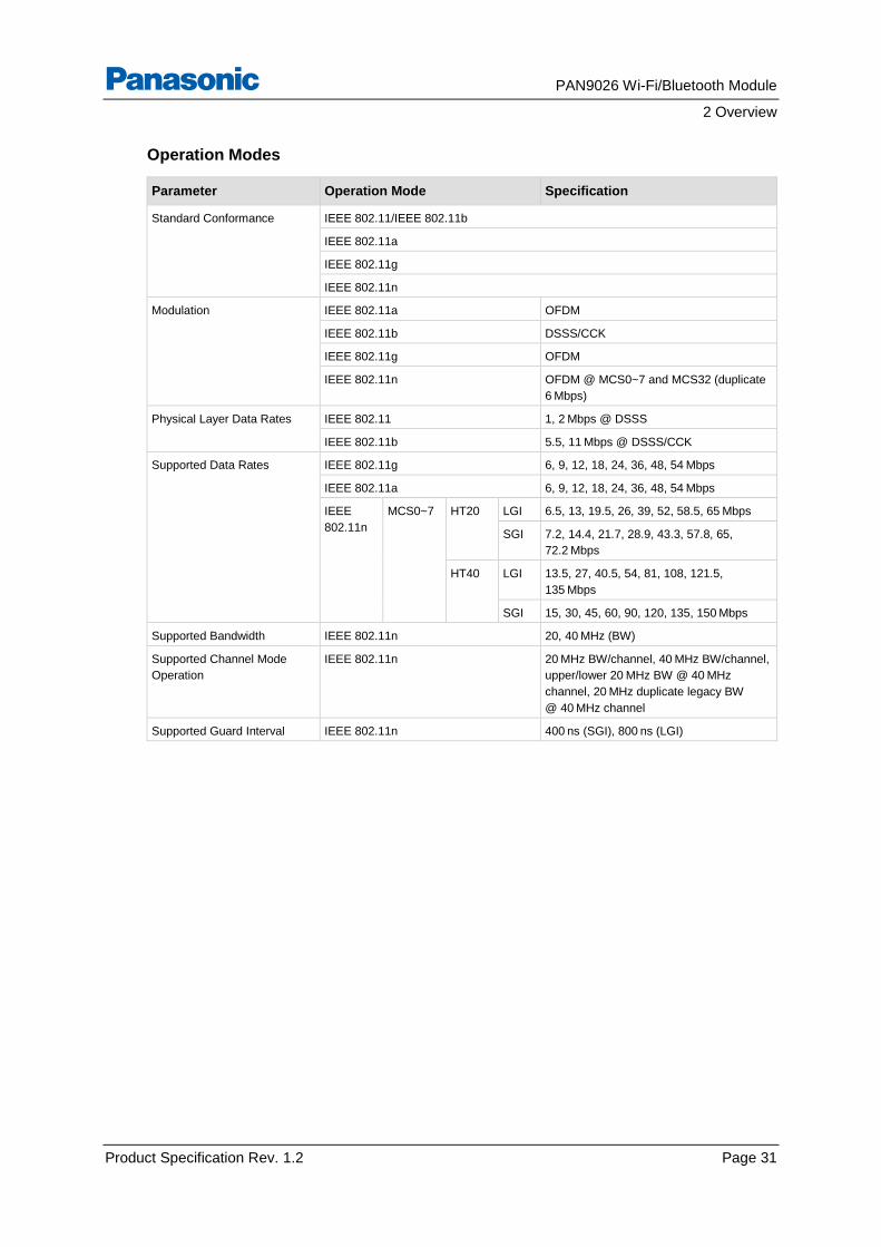
Operation Modes
Parameter Operation Mode Specification
Standard Conformance IEEE 802.11/IEEE 802.11b
IEEE 802.11a
IEEE 802.11g
IEEE 802.11n
Modulation IEEE 802.11a OFDM
IEEE 802.11b DSSS/CCK
IEEE 802.11g OFDM
IEEE 802.11n OFDM @ MCS0~7 and MCS32 (duplicate
6 Mbps)
Physical Layer Data Rates IEEE 802.11 1, 2 Mbps @ DSSS
IEEE 802.11b 5.5, 11 Mbps @ DSSS/CCK
Supported Data Rates IEEE 802.11g 6, 9, 12, 18, 24, 36, 48, 54 Mbps
IEEE 802.11a 6, 9, 12, 18, 24, 36, 48, 54 Mbps
IEEE
802.11n
MCS0~7 HT20
LGI 6.5, 13, 19.5, 26, 39, 52, 58.5, 65 Mbps
SGI 7.2, 14.4, 21.7, 28.9, 43.3, 57.8, 65,
72.2 Mbps
HT40 LGI 13.5, 27, 40.5, 54, 81, 108, 121.5,
135 Mbps
SGI 15, 30, 45, 60, 90, 120, 135, 150 Mbps
Supported Bandwidth IEEE 802.11n 20, 40 MHz (BW)
Supported Channel Mode
Operation
IEEE 802.11n 20 MHz BW/channel, 40 MHz BW/channel,
upper/lower 20 MHz BW @ 40 MHz
channel, 20 MHz duplicate legacy BW
@ 40 MHz channel
Supported Guard Interval IEEE 802.11n 400 ns (SGI), 800 ns (LGI)
PAN9026 Wi-Fi/Bluetooth Module
2 Overview
Product Specification Rev. 1.2 Page 32
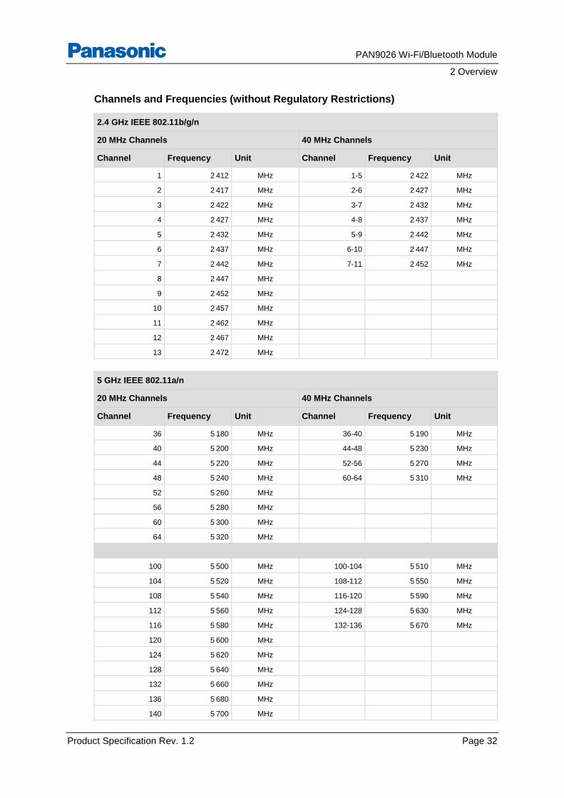
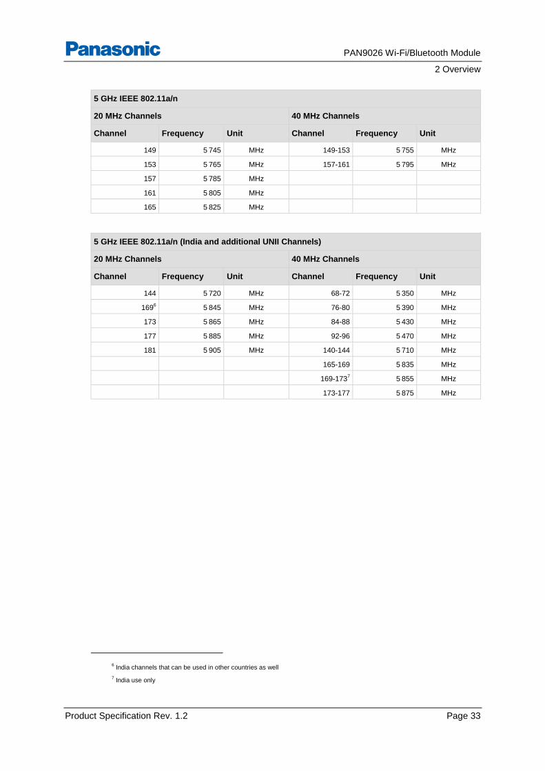
Channels and Frequencies (without Regulatory Restrictions)
2.4 GHz IEEE 802.11b/g/n
20 MHz Channels 40 MHz Channels
Channel Frequency Unit Channel Frequency Unit
1 2 412 MHz 1-5 2 422 MHz
2 2 417 MHz 2-6 2 427 MHz
3 2 422 MHz 3-7 2 432 MHz
4 2 427 MHz 4-8 2 437 MHz
5 2 432 MHz 5-9 2 442 MHz
6 2 437 MHz 6-10 2 447 MHz
7 2 442 MHz 7-11 2 452 MHz
8 2 447 MHz
9 2 452 MHz
10 2 457 MHz
11 2 462 MHz
12 2 467 MHz
13 2 472 MHz
5 GHz IEEE 802.11a/n
20 MHz Channels 40 MHz Channels
Channel Frequency Unit Channel Frequency Unit
36 5 180 MHz 36-40 5 190 MHz
40 5 200 MHz 44-48 5 230 MHz
44 5 220 MHz 52-56 5 270 MHz
48 5 240 MHz 60-64 5 310 MHz
52 5 260 MHz
56 5 280 MHz
60 5 300 MHz
64 5 320 MHz
100 5 500 MHz 100-104 5 510 MHz
104 5 520 MHz 108-112 5 550 MHz
108 5 540 MHz 116-120 5 590 MHz
112 5 560 MHz 124-128 5 630 MHz
116 5 580 MHz 132-136 5 670 MHz
120 5 600 MHz
124 5 620 MHz
128 5 640 MHz
132 5 660 MHz
136 5 680 MHz
140 5 700 MHz
PAN9026 Wi-Fi/Bluetooth Module
2 Overview
Product Specification Rev. 1.2 Page 33
5 GHz IEEE 802.11a/n
20 MHz Channels 40 MHz Channels
Channel Frequency Unit Channel Frequency Unit
149 5 745 MHz 149-153 5 755 MHz
153 5 765 MHz 157-161 5 795 MHz
157 5 785 MHz
161 5 805 MHz
165 5 825 MHz
5 GHz IEEE 802.11a/n (India and additional UNII Channels)
20 MHz Channels 40 MHz Channels
Channel Frequency Unit Channel Frequency Unit
144 5 720 MHz 68-72 5 350 MHz
1696 5 845 MHz 76-80 5 390 MHz
173 5 865 MHz 84-88 5 430 MHz
177 5 885 MHz 92-96 5 470 MHz
181 5 905 MHz 140-144 5 710 MHz
165-169 5 835 MHz
169-1737 5 855 MHz
173-177 5 875 MHz
6 India channels that can be used in other countries as well
7 India use only
PAN9026 Wi-Fi/Bluetooth Module
2 Overview
Product Specification Rev. 1.2 Page 34
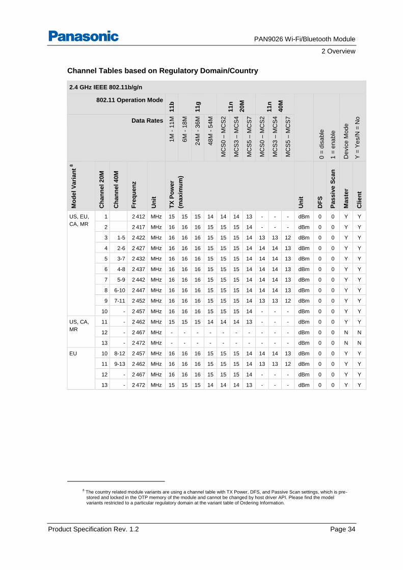
Channel Tables based on Regulatory Domain/Country
2.4 GHz IEEE 802.11b/g/n
802.11 Operation Mode
11
b
11
g
11
n
20
M
11
n
40
M
0 =
dis
able
1 =
ena
ble
De
vic
e M
od
e
Y =
Ye
s/N
= N
o
Data Rates
1M
- 1
1M
6M
- 1
8M
24
M -
36M
48
M -
54M
MC
S0
– M
CS
2
MC
S3
– M
CS
4
MC
S5
– M
CS
7
MC
S0
– M
CS
2
MC
S3
– M
CS
4
MC
S5
– M
CS
7
Mo
de
l V
ari
an
t 8
Ch
an
ne
l 2
0M
Ch
an
ne
l 4
0M
Fre
qu
en
z
Un
it
TX
Po
we
r
(ma
xim
um
)
Un
it
DF
S
Pa
ss
ive
Sc
an
Ma
ste
r
Cli
en
t
US, EU,
CA, MR
1 2 412 MHz 15 15 15 14 14 14 13 - - - dBm 0 0 Y Y
2 2 417 MHz 16 16 16 15 15 15 14 - - - dBm 0 0 Y Y
3 1-5 2 422 MHz 16 16 16 15 15 15 14 13 13 12 dBm 0 0 Y Y
4 2-6 2 427 MHz 16 16 16 15 15 15 14 14 14 13 dBm 0 0 Y Y
5 3-7 2 432 MHz 16 16 16 15 15 15 14 14 14 13 dBm 0 0 Y Y
6 4-8 2 437 MHz 16 16 16 15 15 15 14 14 14 13 dBm 0 0 Y Y
7 5-9 2 442 MHz 16 16 16 15 15 15 14 14 14 13 dBm 0 0 Y Y
8 6-10 2 447 MHz 16 16 16 15 15 15 14 14 14 13 dBm 0 0 Y Y
9 7-11 2 452 MHz 16 16 16 15 15 15 14 13 13 12 dBm 0 0 Y Y
10 - 2 457 MHz 16 16 16 15 15 15 14 - - - dBm 0 0 Y Y
US, CA,
MR
11 - 2 462 MHz 15 15 15 14 14 14 13 - - - dBm 0 0 Y Y
12 - 2 467 MHz - - - - - - - - - - dBm 0 0 N N
13 - 2 472 MHz - - - - - - - - - - dBm 0 0 N N
EU 10 8-12 2 457 MHz 16 16 16 15 15 15 14 14 14 13 dBm 0 0 Y Y
11 9-13 2 462 MHz 16 16 16 15 15 15 14 13 13 12 dBm 0 0 Y Y
12 - 2 467 MHz 16 16 16 15 15 15 14 - - - dBm 0 0 Y Y
13 - 2 472 MHz 15 15 15 14 14 14 13 - - - dBm 0 0 Y Y
8 The country related module variants are using a channel table with TX Power, DFS, and Passive Scan settings, which is pre-stored and locked in the OTP memory of the module and cannot be changed by host driver API. Please find the model variants restricted to a particular regulatory domain at the variant table of Ordering Information.
PAN9026 Wi-Fi/Bluetooth Module
2 Overview
Product Specification Rev. 1.2 Page 35
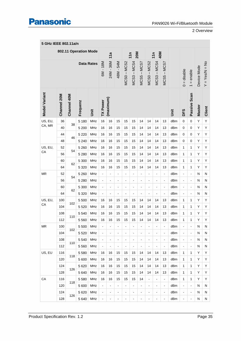
5 GHz IEEE 802.11a/n
802.11 Operation Mode
11
a
11
n
20
M
11
n
40
M
0 =
dis
able
1 =
ena
ble
De
vic
e M
od
e
Y =
Ye
s/N
= N
o
Data Rates
6M
- 1
8M
24
M -
36M
48
M -
54M
MC
S0
– M
CS
2
MC
S3
– M
CS
4
MC
S5
– M
CS
7
MC
S0
– M
CS
2
MC
S3
– M
CS
4
MC
S5
– M
CS
7
Mo
de
l V
ari
an
t
Ch
an
ne
l 2
0M
Ch
an
ne
l 4
0M
Fre
qu
en
z
Un
it
TX
Po
we
r
(ma
xim
um
)
Un
it
DF
S
Pa
ss
ive
Sc
an
Ma
ste
r
Cli
en
t
US, EU,
CA, MR
36 38
5 180 MHz 16 16 15 15 15 14 14 14 13 dBm 0 0 Y Y
40 5 200 MHz 16 16 15 15 15 14 14 14 13 dBm 0 0 Y Y
44 46
5 220 MHz 16 16 15 15 15 14 14 14 13 dBm 0 0 Y Y
48 5 240 MHz 16 16 15 15 15 14 14 14 13 dBm 0 0 Y Y
US, EU,
CA
52 54
5 260 MHz 16 16 15 15 15 14 14 14 13 dBm 1 1 Y Y
56 5 280 MHz 16 16 15 15 15 14 14 14 13 dBm 1 1 Y Y
60 62
5 300 MHz 16 16 15 15 15 14 14 14 13 dBm 1 1 Y Y
64 5 320 MHz 16 16 15 15 15 14 14 14 13 dBm 1 1 Y Y
MR 52 54
5 260 MHz - - - - - - - - - dBm - - N N
56 5 280 MHz - - - - - - - - - dBm - - N N
60 62
5 300 MHz - - - - - - - - - dBm - - N N
64 5 320 MHz - - - - - - - - - dBm - - N N
US, EU,
CA
100 102
5 500 MHz 16 16 15 15 15 14 14 14 13 dBm 1 1 Y Y
104 5 520 MHz 16 16 15 15 15 14 14 14 13 dBm 1 1 Y Y
108 110
5 540 MHz 16 16 15 15 15 14 14 14 13 dBm 1 1 Y Y
112 5 560 MHz 16 16 15 15 15 14 14 14 13 dBm 1 1 Y Y
MR 100 102
5 500 MHz - - - - - - - - - dBm - - N N
104 5 520 MHz - - - - - - - - - dBm - - N N
108 110
5 540 MHz - - - - - - - - - dBm - - N N
112 5 560 MHz - - - - - - - - - dBm - - N N
US, EU 116 118
5 580 MHz 16 16 15 15 15 14 14 14 13 dBm 1 1 Y Y
120 5 600 MHz 16 16 15 15 15 14 14 14 13 dBm 1 1 Y Y
124 126
5 620 MHz 16 16 15 15 15 14 14 14 13 dBm 1 1 Y Y
128 5 640 MHz 16 16 15 15 15 14 14 14 13 dBm 1 1 Y Y
CA 116 118
5 580 MHz 16 16 15 15 15 14 - - - dBm 1 1 Y Y
120 5 600 MHz - - - - - - - - - dBm - - N N
124 126
5 620 MHz - - - - - - - - - dBm - - N N
128 5 640 MHz - - - - - - - - - dBm - - N N
PAN9026 Wi-Fi/Bluetooth Module
2 Overview
Product Specification Rev. 1.2 Page 36
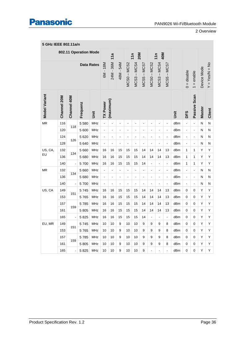
5 GHz IEEE 802.11a/n
802.11 Operation Mode
11
a
11
n
20
M
11
n
40
M
0 =
dis
able
1 =
ena
ble
De
vic
e M
od
e
Y =
Ye
s/N
= N
o
Data Rates
6M
- 1
8M
24
M -
36M
48
M -
54M
MC
S0
– M
CS
2
MC
S3
– M
CS
4
MC
S5
– M
CS
7
MC
S0
– M
CS
2
MC
S3
– M
CS
4
MC
S5
– M
CS
7
Mo
de
l V
ari
an
t
Ch
an
ne
l 2
0M
Ch
an
ne
l 4
0M
Fre
qu
en
z
Un
it
TX
Po
we
r
(ma
xim
um
)
Un
it
DF
S
Pa
ss
ive
Sc
an
Ma
ste
r
Cli
en
t
MR 116 118
5 580 MHz - - - - - - - - - dBm - - N N
120 5 600 MHz - - - - - - - - - dBm - - N N
124 126
5 620 MHz - - - - - - - - - dBm - - N N
128 5 640 MHz - - - - - - - - - dBm - - N N
US, CA,
EU
132 134
5 660 MHz 16 16 15 15 15 14 14 14 13 dBm 1 1 Y Y
136 5 680 MHz 16 16 15 15 15 14 14 14 13 dBm 1 1 Y Y
140 - 5 700 MHz 16 16 15 15 15 14 - - - dBm 1 1 Y Y
MR 132 134
5 660 MHz - - - - - - - - - dBm - - N N
136 5 680 MHz - - - - - - - - - dBm - - N N
140 - 5 700 MHz - - - - - - - - - dBm - - N N
US, CA 149 151
5 745 MHz 16 16 15 15 15 14 14 14 13 dBm 0 0 Y Y
153 5 765 MHz 16 16 15 15 15 14 14 14 13 dBm 0 0 Y Y
157 159
5 785 MHz 16 16 15 15 15 14 14 14 13 dBm 0 0 Y Y
161 5 805 MHz 16 16 15 15 15 14 14 14 13 dBm 0 0 Y Y
165 - 5 825 MHz 16 16 15 15 15 14 - - - dBm 0 0 Y Y
EU, MR 149 151
5 745 MHz 10 10 9 10 10 9 9 9 8 dBm 0 0 Y Y
153 5 765 MHz 10 10 9 10 10 9 9 9 8 dBm 0 0 Y Y
157 159
5 785 MHz 10 10 9 10 10 9 9 9 8 dBm 0 0 Y Y
161 5 805 MHz 10 10 9 10 10 9 9 9 8 dBm 0 0 Y Y
165 - 5 825 MHz 10 10 9 10 10 9 - - - dBm 0 0 Y Y
PAN9026 Wi-Fi/Bluetooth Module
2 Overview
Product Specification Rev. 1.2 Page 37
2.9 Bluetooth
Type Features
General • Supports Bluetooth 5.0
• Shared Tx/Rx path for Bluetooth
• Digital Audio Interface including PCM interface for voice application
• Bluetooth and WLAN coexistence
• WLAN/Bluetooth Coexistence (BCA) protocol support
Bluetooth Classic
(BR/EDR)
• Bluetooth Classic with Bluetooth Class 1 support
• Baseband and radio Basic Rate (BR) and Enhanced Data Rate (EDR) packet types with 1 Mbps (GFSK), 2 Mbps (π/4-DQPSK) and 3 Mbps (8DPSK)
• Fully functional Bluetooth baseband with: – Adaptive Frequency Hopping (AFH) – Forward error correction – Header error control – Access code correlation – CRC – Encryption bit stream generation – Whitening
• Adaptive Frequency Hopping (AFH) including Packet Loss Rate (PLR)
• Interlaced scan for faster connection setup
• Simultaneous active ACL connection support
• Automatic ACL packet type selection
• Full master slave piconet support
• Scatternet support
• Standard UART and SDIO HCI transport layer
• SCO/eSCO links with hardware accelerated audio signal pocessing and hardware supported PPEC algorithm for speech quality improvement
• All standard SCO/eSCO voice coding
• All standard pairing, authentication, link key, and encryption operations
• Standard Bluetooth power saving mechanism (i.e. hold, sniff modes, and sniff-sub rating)
• Enhanced Power Control (EPC)
• Channel Quality Driven (CQD) data rate
• Wideband Speech (WBS) support (1 WBS link)
• Encryption (AES) support
• LTE/MWS coexistence
PAN9026 Wi-Fi/Bluetooth Module
2 Overview
Product Specification Rev. 1.2 Page 38
Type Features
Bluetooth Low Energy (LE) • Broadcaster, Observer, Central, and Peripheral roles
• Supports link layer topology to be master and slave (connects up to 16 links)
• Shared RF with BR/EDR
• Encryption AES support
• Hardware support for intelligent Adaptive Frequency Hopping (AFH)
• LE Privacy 1.2
• LE Secure Connection
• LE Data Length Extension
• LE Advertising Length Extension
• Direction Finding, Connection-oriented Angle of Arrival (AoA)
PAN9026 Wi-Fi/Bluetooth Module
3 Detailed Description
Product Specification Rev. 1.2 Page 39
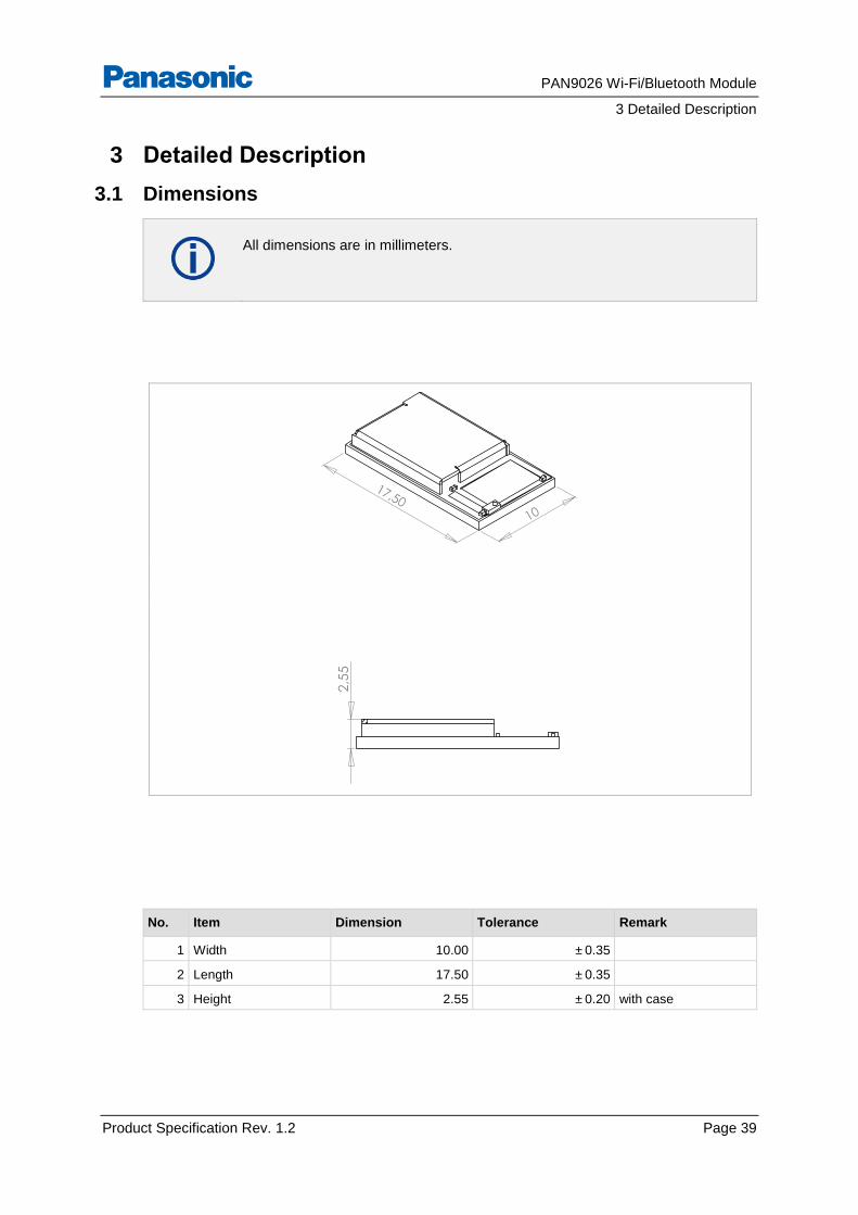
3 Detailed Description
3.1 Dimensions
All dimensions are in millimeters.
No. Item Dimension Tolerance Remark
1 Width 10.00 ± 0.35
2 Length 17.50 ± 0.35
3 Height 2.55 ± 0.20 with case
17,50
10
2,5
5
PAN9026 Wi-Fi/Bluetooth Module
3 Detailed Description
Product Specification Rev. 1.2 Page 40
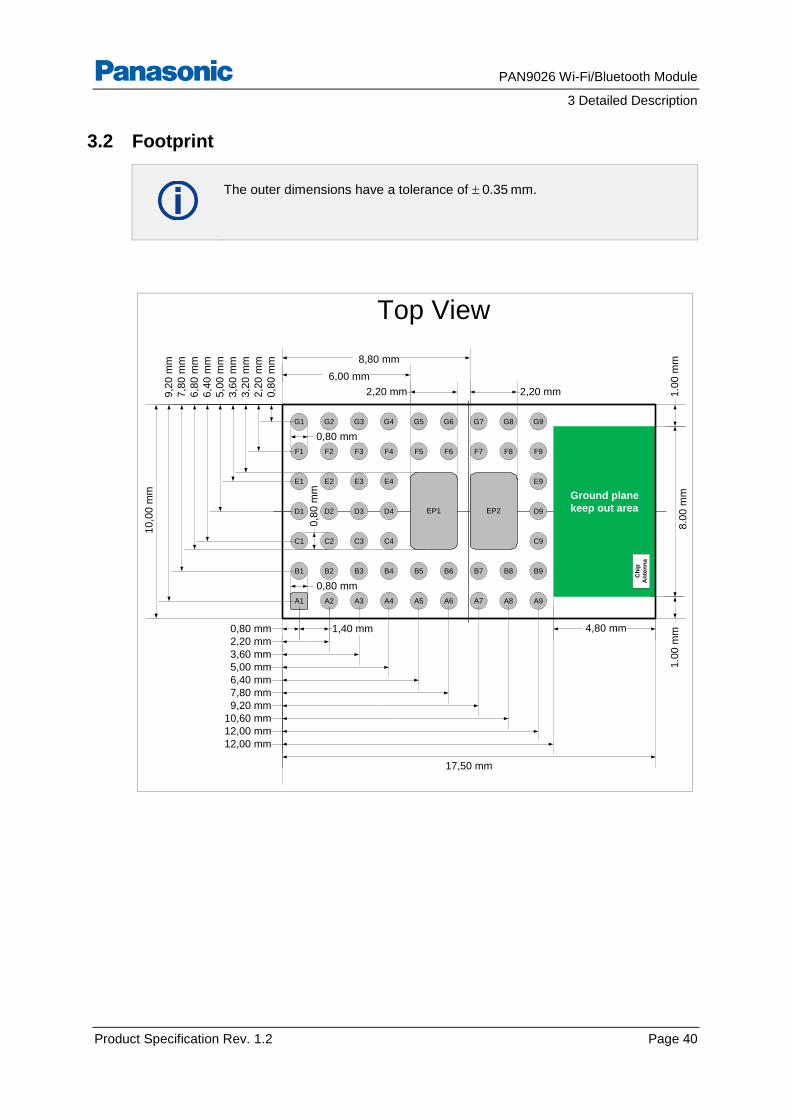
3.2 Footprint
The outer dimensions have a tolerance of 0.35 mm.
8,80 mm
2,20 mm2,20 mm
6,00 mm
3,2
0 m
m
6,8
0 m
m
0,8
0 m
m
0,80 mm
0,80 mm
A1
B1
C1
D1
E1
F1
A2
B2
C2
D2
E2
F2
G2
A3
B3
C3
D3
E3
F3
G3
A4
B4
C4
D4
E4
F4
G4
A5
B5
F5
G5
A6
B6
F6
G6
A7
B7
F7
G7
A8
B8
F8
G8
A9
B9
C9
D9
E9
F9
G9
Ch
ip
An
ten
na
0,80 mm
2,20 mm
3,60 mm
5,00 mm
17,50 mm
6,40 mm
7,80 mm
9,20 mm
10,60 mm
12,00 mm
1,40 mm
12,00 mm
4,80 mm
8.0
0 m
m1
.00
mm
1
.00
mm
2,2
0 m
m
0,8
0 m
m
3,6
0 m
m
5,0
0 m
m
6,4
0 m
m
7,8
0 m
m
9,2
0 m
m
10
,00 m
m Ground plane
keep out area
Top View
G1
EP1 EP2
PAN9026 Wi-Fi/Bluetooth Module
3 Detailed Description
Product Specification Rev. 1.2 Page 41
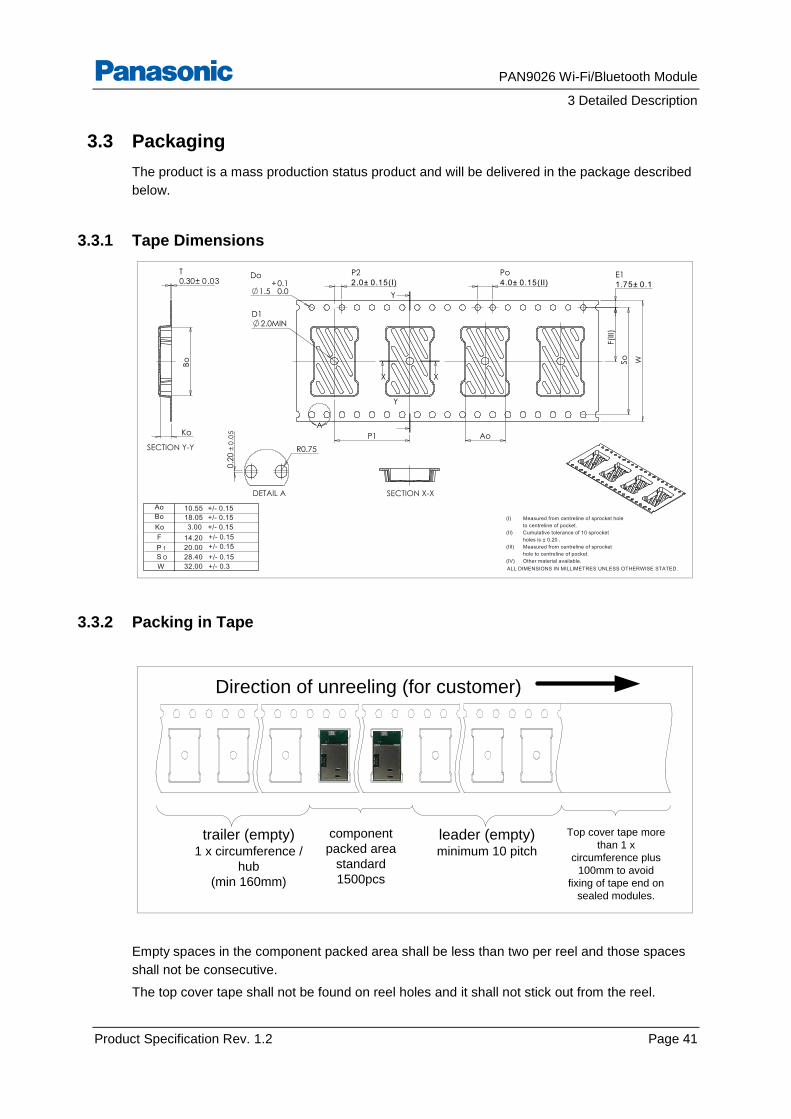
3.3 Packaging
The product is a mass production status product and will be delivered in the package described
below.
3.3.1 Tape Dimensions
3.3.2 Packing in Tape
Empty spaces in the component packed area shall be less than two per reel and those spaces
shall not be consecutive.
The top cover tape shall not be found on reel holes and it shall not stick out from the reel.
W
Do
1.5 +0.1
0.0
PoP2 E1
Ao
D12.0MIN
F(I
II)
So
P1
X X
A
Y
Y
SECTION X-X
0.2
0 ±
0.0
5
R0.75
DETAIL A
Ko
T0.30± 0.03
Bo
SECTION Y-Y
Measured from centreline of sprocket hole
to centreline of pocket.
Cumulative tolerance of 10 sprocket
holes is ± 0.20 .
Measured from centreline of sprocket
hole to centreline of pocket.
(I)
(II)
(III)
(IV) Other material available.
ALL DIMENSIONS IN MILLIMETRES UNLESS OTHERWISE STATED.W
F
S O
+/- 0.15
+/- 0.15
+/- 0.3
14.20
28.40
32.00
Ao
18.05 +/- 0.15Bo
3.00 +/- 0.15
20.00P 1 +/- 0.15
Ko
10.55 +/- 0.15
2.0± 0.15(I) 4.0± 0.15(II) 1.75± 0.1
100730-PAN1720.vsd
trailer (empty)1 x circumference /
hub
(min 160mm)
component
packed area
standard
1500pcs
leader (empty)minimum 10 pitch
Top cover tape more
than 1 x
circumference plus
100mm to avoid
fixing of tape end on
sealed modules.
Direction of unreeling (for customer)
PAN9026 Wi-Fi/Bluetooth Module
3 Detailed Description
Product Specification Rev. 1.2 Page 42
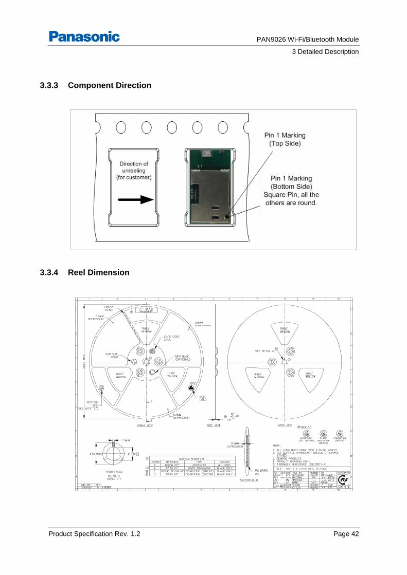
3.3.3 Component Direction
3.3.4 Reel Dimension
PAN9026 Wi-Fi/Bluetooth Module
3 Detailed Description
Product Specification Rev. 1.2 Page 43
3.3.5 Package Label
Example
(1T)
(1P)
(2P)
(9D)
(Q)
(HW/SW)
Lot code
Customer order number, if applicable
Order number
Date code
Quantity
Hardware/software version
3.3.6 Total Package
barcode
label
moisture-sensitive print
(already exist on barrier bag)barcode
label
desiccant 1) 2)
moisture indicator
barrier bag
sealed
inner carton box
size 340 x 340 x 41 mm³
1) quantity of desiccant according
to calculation
2) optional: desiccant placed into
the corner of the barrier bag
PAN9026 Wi-Fi/Bluetooth Module
3 Detailed Description
Product Specification Rev. 1.2 Page 44
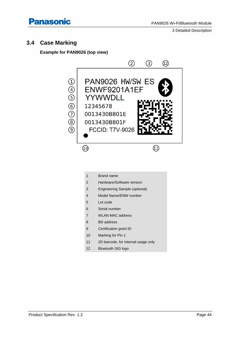
3.4 Case Marking
Example for PAN9026 (top view)
1
2
3
4
5
6
7
8
9
10
11
12
Brand name
Hardware/Software version
Engineering Sample (optional)
Model Name/ENW number
Lot code
Serial number
WLAN MAC address
BD address
Certification grant ID
Marking for Pin 1
2D barcode, for internal usage only
Bluetooth SIG logo
PAN9026 Wi-Fi/Bluetooth Module
4 Specification
Product Specification Rev. 1.2 Page 45
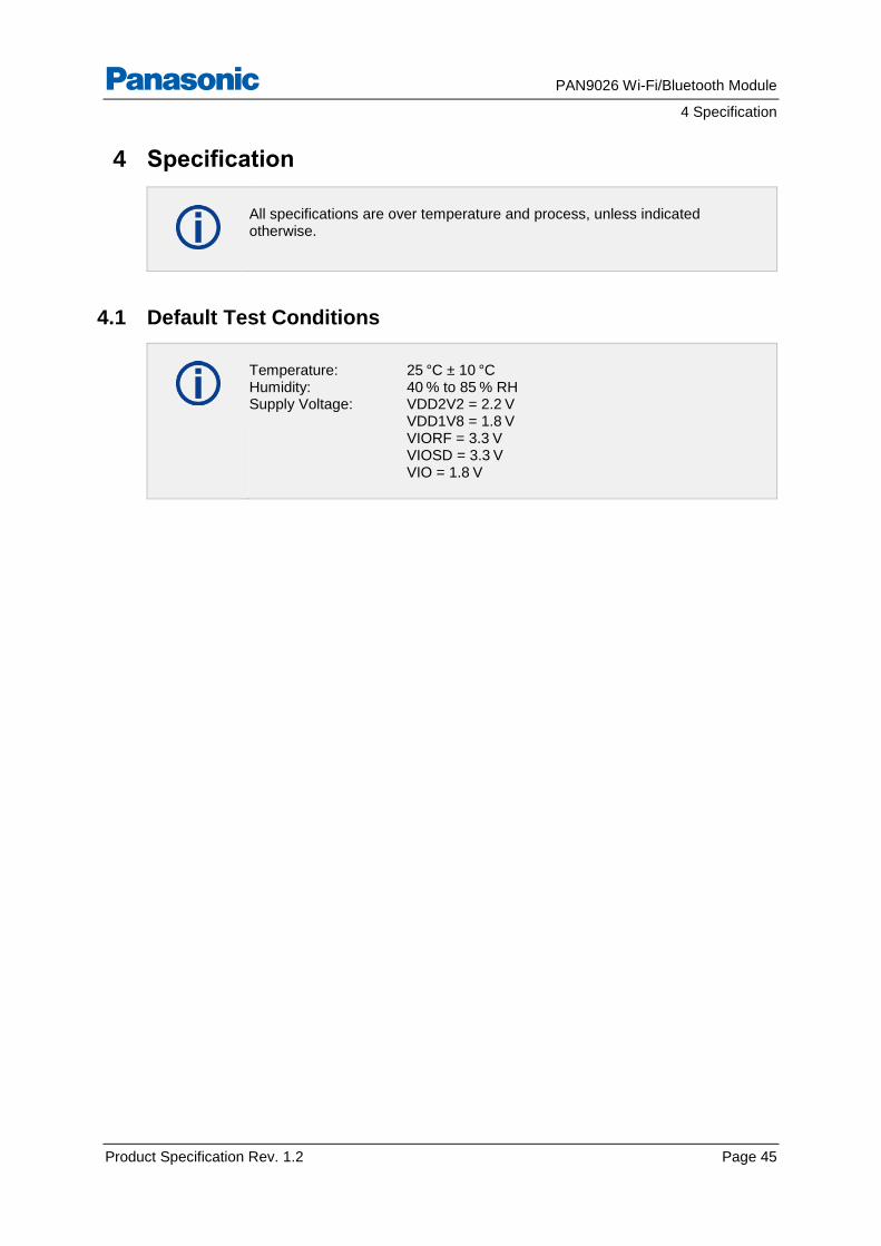
4 Specification
All specifications are over temperature and process, unless indicated otherwise.
4.1 Default Test Conditions
Temperature: 25 °C ± 10 °C Humidity: 40 % to 85 % RH Supply Voltage: VDD2V2 = 2.2 V VDD1V8 = 1.8 V VIORF = 3.3 V VIOSD = 3.3 V VIO = 1.8 V
PAN9026 Wi-Fi/Bluetooth Module
4 Specification
Product Specification Rev. 1.2 Page 46
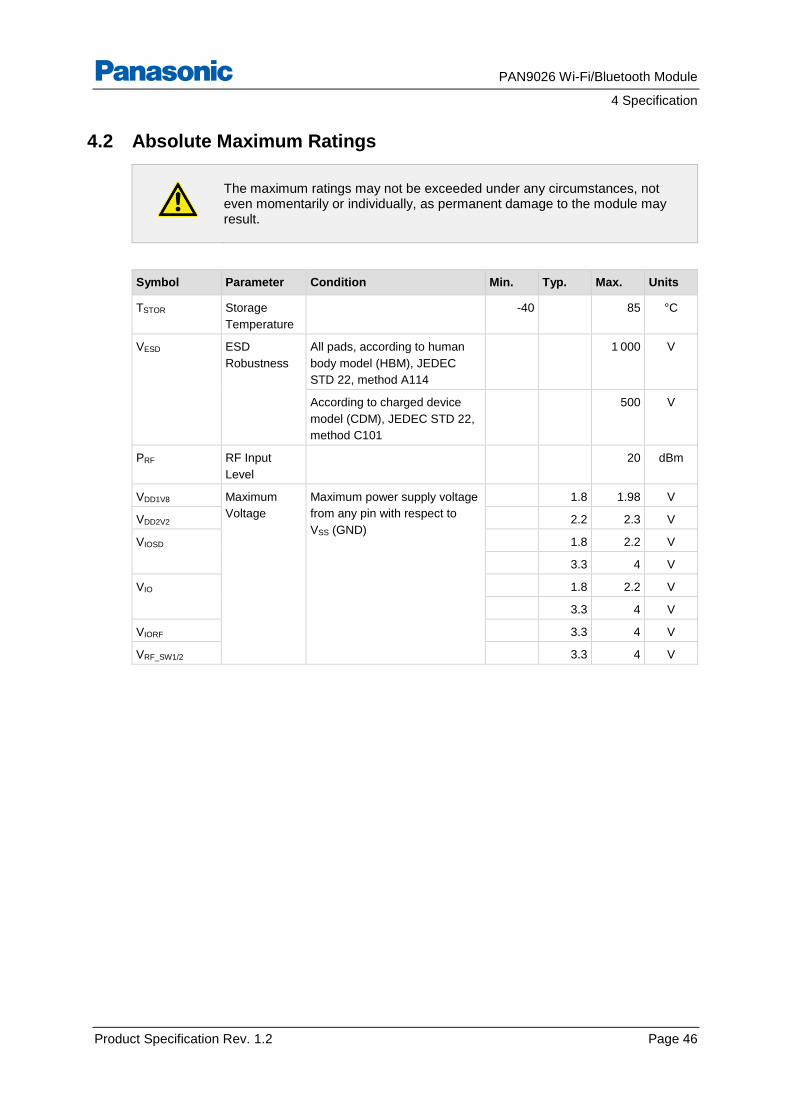
4.2 Absolute Maximum Ratings
The maximum ratings may not be exceeded under any circumstances, not even momentarily or individually, as permanent damage to the module may result.
Symbol Parameter Condition Min. Typ. Max. Units
TSTOR Storage
Temperature
-40 85 °C
VESD ESD
Robustness
All pads, according to human
body model (HBM), JEDEC
STD 22, method A114
1 000 V
According to charged device
model (CDM), JEDEC STD 22,
method C101
500 V
PRF RF Input
Level
20 dBm
VDD1V8 Maximum
Voltage
Maximum power supply voltage
from any pin with respect to
VSS (GND)
1.8 1.98 V
VDD2V2 2.2 2.3 V
VIOSD 1.8 2.2 V
3.3 4 V
VIO 1.8 2.2 V
3.3 4 V
VIORF 3.3 4 V
VRF_SW1/2 3.3 4 V
PAN9026 Wi-Fi/Bluetooth Module
4 Specification
Product Specification Rev. 1.2 Page 47
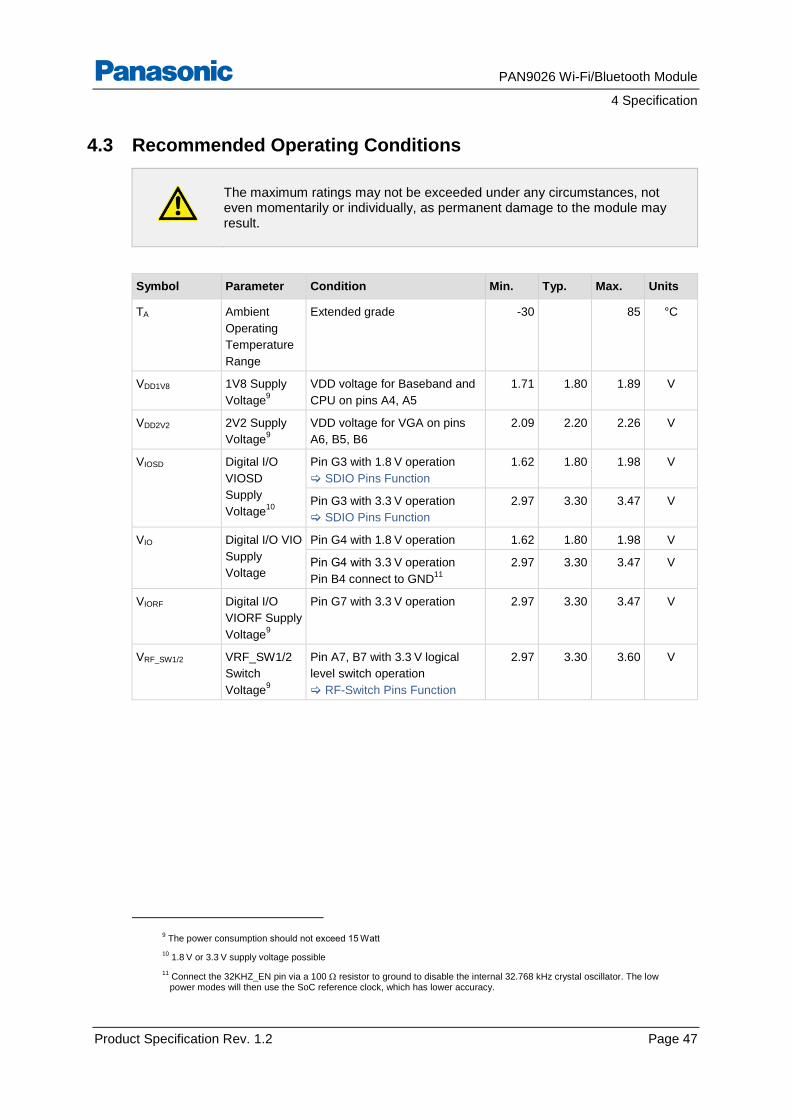
4.3 Recommended Operating Conditions
The maximum ratings may not be exceeded under any circumstances, not even momentarily or individually, as permanent damage to the module may result.
Symbol Parameter Condition Min. Typ. Max. Units
TA Ambient
Operating
Temperature
Range
Extended grade -30 85 °C
VDD1V8 1V8 Supply
Voltage9
VDD voltage for Baseband and
CPU on pins A4, A5
1.71 1.80 1.89 V
VDD2V2 2V2 Supply
Voltage9
VDD voltage for VGA on pins
A6, B5, B6
2.09 2.20 2.26 V
VIOSD Digital I/O
VIOSD
Supply
Voltage10
Pin G3 with 1.8 V operation
SDIO Pins Function
1.62 1.80 1.98 V
Pin G3 with 3.3 V operation
SDIO Pins Function
2.97 3.30 3.47 V
VIO Digital I/O VIO
Supply
Voltage
Pin G4 with 1.8 V operation 1.62 1.80 1.98 V
Pin G4 with 3.3 V operation
Pin B4 connect to GND11
2.97 3.30 3.47 V
VIORF Digital I/O
VIORF Supply
Voltage9
Pin G7 with 3.3 V operation 2.97 3.30 3.47 V
VRF_SW1/2 VRF_SW1/2
Switch
Voltage9
Pin A7, B7 with 3.3 V logical
level switch operation
RF-Switch Pins Function
2.97 3.30 3.60 V
9 The power consumption should not exceed 15 Watt
10 1.8 V or 3.3 V supply voltage possible
11 Connect the 32KHZ_EN pin via a 100 resistor to ground to disable the internal 32.768 kHz crystal oscillator. The low power modes will then use the SoC reference clock, which has lower accuracy.
PAN9026 Wi-Fi/Bluetooth Module
4 Specification
Product Specification Rev. 1.2 Page 48
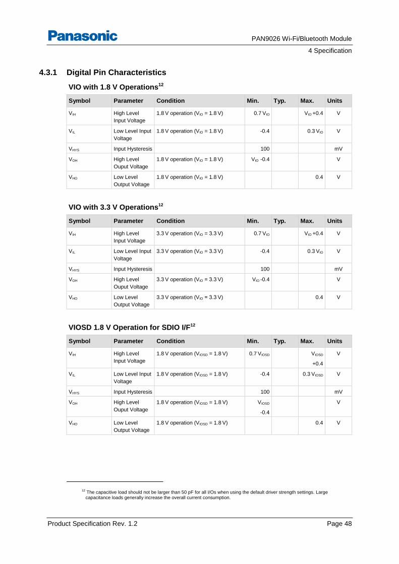
4.3.1 Digital Pin Characteristics
VIO with 1.8 V Operations12
Symbol Parameter Condition Min. Typ. Max. Units
VIH High Level
Input Voltage
1.8 V operation (VIO = 1.8 V) 0.7 VIO VIO +0.4 V
VIL Low Level Input
Voltage
1.8 V operation (VIO = 1.8 V) -0.4 0.3 VIO V
VHYS Input Hysteresis 100 mV
VOH High Level
Ouput Voltage
1.8 V operation (VIO = 1.8 V) VIO -0.4 V
VHO Low Level
Output Voltage
1.8 V operation (VIO = 1.8 V) 0.4 V
VIO with 3.3 V Operations12
Symbol Parameter Condition Min. Typ. Max. Units
VIH High Level
Input Voltage
3.3 V operation (VIO = 3.3 V) 0.7 VIO VIO +0.4 V
VIL Low Level Input
Voltage
3.3 V operation (VIO = 3.3 V) -0.4 0.3 VIO V
VHYS Input Hysteresis 100 mV
VOH High Level
Ouput Voltage
3.3 V operation (VIO = 3.3 V) VIO -0.4 V
VHO Low Level
Output Voltage
3.3 V operation (VIO = 3.3 V) 0.4 V
VIOSD 1.8 V Operation for SDIO I/F12
Symbol Parameter Condition Min. Typ. Max. Units
VIH High Level
Input Voltage
1.8 V operation (VIOSD = 1.8 V) 0.7 VIOSD VIOSD
+0.4
V
VIL Low Level Input
Voltage
1.8 V operation (VIOSD = 1.8 V) -0.4 0.3 VIOSD V
VHYS Input Hysteresis 100 mV
VOH High Level
Ouput Voltage
1.8 V operation (VIOSD = 1.8 V) VIOSD
-0.4
V
VHO Low Level
Output Voltage
1.8 V operation (VIOSD = 1.8 V) 0.4 V
12
The capacitive load should not be larger than 50 pF for all I/Os when using the default driver strength settings. Large capacitance loads generally increase the overall current consumption.
PAN9026 Wi-Fi/Bluetooth Module
4 Specification
Product Specification Rev. 1.2 Page 49
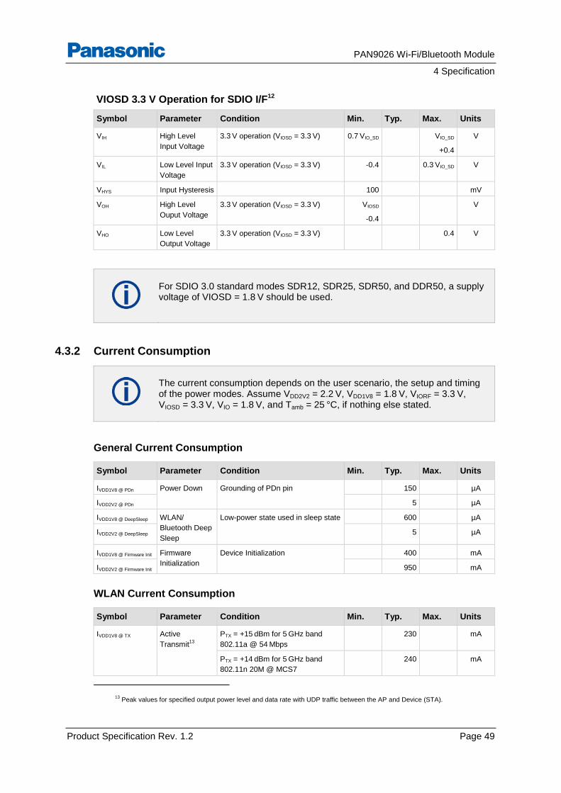
VIOSD 3.3 V Operation for SDIO I/F12
Symbol Parameter Condition Min. Typ. Max. Units
VIH High Level
Input Voltage
3.3 V operation (VIOSD = 3.3 V) 0.7 VIO_SD VIO_SD
+0.4
V
VIL Low Level Input
Voltage
3.3 V operation (VIOSD = 3.3 V) -0.4 0.3 VIO_SD V
VHYS Input Hysteresis 100 mV
VOH High Level
Ouput Voltage
3.3 V operation (VIOSD = 3.3 V) VIOSD
-0.4
V
VHO Low Level
Output Voltage
3.3 V operation (VIOSD = 3.3 V) 0.4 V
For SDIO 3.0 standard modes SDR12, SDR25, SDR50, and DDR50, a supply voltage of VIOSD = 1.8 V should be used.
4.3.2 Current Consumption
The current consumption depends on the user scenario, the setup and timing of the power modes. Assume VDD2V2 = 2.2 V, VDD1V8 = 1.8 V, VIORF = 3.3 V, VIOSD = 3.3 V, VIO = 1.8 V, and Tamb = 25 °C, if nothing else stated.
General Current Consumption
Symbol Parameter Condition Min. Typ. Max. Units
IVDD1V8 @ PDn Power Down Grounding of PDn pin 150 µA
IVDD2V2 @ PDn 5 µA
IVDD1V8 @ DeepSleep WLAN/
Bluetooth Deep
Sleep
Low-power state used in sleep state 600 µA
IVDD2V2 @ DeepSleep 5 µA
IVDD1V8 @ Firmware Init Firmware
Initialization
Device Initialization 400 mA
IVDD2V2 @ Firmware Init 950 mA
WLAN Current Consumption
Symbol Parameter Condition Min. Typ. Max. Units
IVDD1V8 @ TX Active
Transmit13
PTX = +15 dBm for 5 GHz band
802.11a @ 54 Mbps
230 mA
PTX = +14 dBm for 5 GHz band
802.11n 20M @ MCS7
240 mA
13
Peak values for specified output power level and data rate with UDP traffic between the AP and Device (STA).
PAN9026 Wi-Fi/Bluetooth Module
4 Specification
Product Specification Rev. 1.2 Page 50
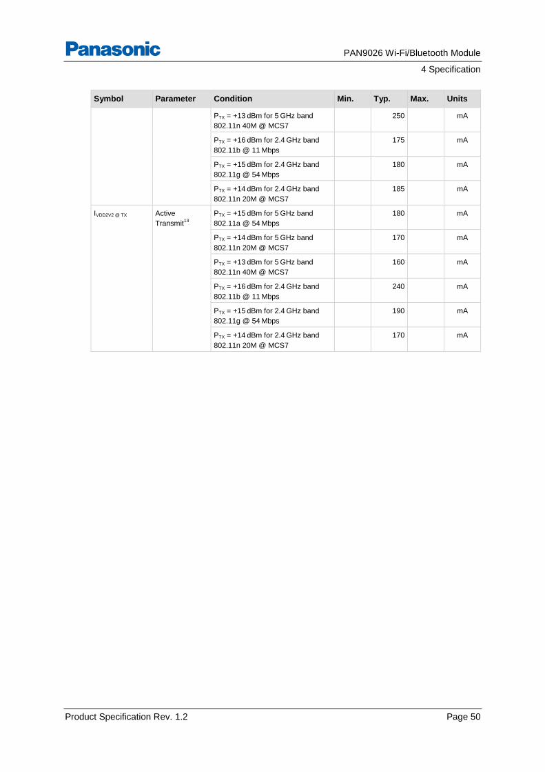
Symbol Parameter Condition Min. Typ. Max. Units
PTX = +13 dBm for 5 GHz band
802.11n 40M @ MCS7
250 mA
PTX = +16 dBm for 2.4 GHz band
802.11b @ 11 Mbps
175 mA
PTX = +15 dBm for 2.4 GHz band
802.11g @ 54 Mbps
180 mA
PTX = +14 dBm for 2.4 GHz band
802.11n 20M @ MCS7
185 mA
IVDD2V2 @ TX Active
Transmit13
PTX = +15 dBm for 5 GHz band
802.11a @ 54 Mbps
180 mA
PTX = +14 dBm for 5 GHz band
802.11n 20M @ MCS7
170 mA
PTX = +13 dBm for 5 GHz band
802.11n 40M @ MCS7
160 mA
PTX = +16 dBm for 2.4 GHz band
802.11b @ 11 Mbps
240 mA
PTX = +15 dBm for 2.4 GHz band
802.11g @ 54 Mbps
190 mA
PTX = +14 dBm for 2.4 GHz band
802.11n 20M @ MCS7
170 mA
PAN9026 Wi-Fi/Bluetooth Module
4 Specification
Product Specification Rev. 1.2 Page 51
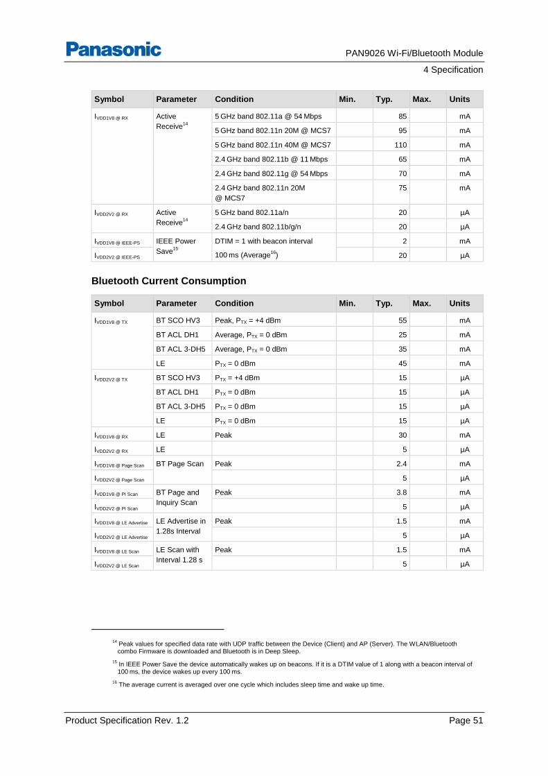
Symbol Parameter Condition Min. Typ. Max. Units
IVDD1V8 @ RX Active
Receive14
5 GHz band 802.11a @ 54 Mbps 85 mA
5 GHz band 802.11n 20M @ MCS7 95 mA
5 GHz band 802.11n 40M @ MCS7 110 mA
2.4 GHz band 802.11b @ 11 Mbps 65 mA
2.4 GHz band 802.11g @ 54 Mbps 70 mA
2.4 GHz band 802.11n 20M
@ MCS7
75 mA
IVDD2V2 @ RX Active
Receive14
5 GHz band 802.11a/n 20 µA
2.4 GHz band 802.11b/g/n 20 µA
IVDD1V8 @ IEEE-PS IEEE Power
Save15
DTIM = 1 with beacon interval
100 ms (Average16
)
2 mA
IVDD2V2 @ IEEE-PS 20 µA
Bluetooth Current Consumption
Symbol Parameter Condition Min. Typ. Max. Units
IVDD1V8 @ TX BT SCO HV3 Peak, PTX = +4 dBm 55 mA
BT ACL DH1 Average, PTX = 0 dBm 25 mA
BT ACL 3-DH5 Average, PTX = 0 dBm 35 mA
LE PTX = 0 dBm 45 mA
IVDD2V2 @ TX BT SCO HV3 PTX = +4 dBm 15 µA
BT ACL DH1 PTX = 0 dBm 15 µA
BT ACL 3-DH5 PTX = 0 dBm 15 µA
LE PTX = 0 dBm 15 µA
IVDD1V8 @ RX LE Peak 30 mA
IVDD2V2 @ RX LE 5 µA
IVDD1V8 @ Page Scan BT Page Scan Peak 2.4 mA
IVDD2V2 @ Page Scan 5 µA
IVDD1V8 @ PI Scan BT Page and
Inquiry Scan
Peak 3.8 mA
IVDD2V2 @ PI Scan 5 µA
IVDD1V8 @ LE Advertise LE Advertise in
1.28s Interval
Peak 1.5 mA
IVDD2V2 @ LE Advertise 5 µA
IVDD1V8 @ LE Scan LE Scan with
Interval 1.28 s
Peak 1.5 mA
IVDD2V2 @ LE Scan 5 µA
14
Peak values for specified data rate with UDP traffic between the Device (Client) and AP (Server). The WLAN/Bluetooth combo Firmware is downloaded and Bluetooth is in Deep Sleep.
15 In IEEE Power Save the device automatically wakes up on beacons. If it is a DTIM value of 1 along with a beacon interval of 100 ms, the device wakes up every 100 ms.
16 The average current is averaged over one cycle which includes sleep time and wake up time.
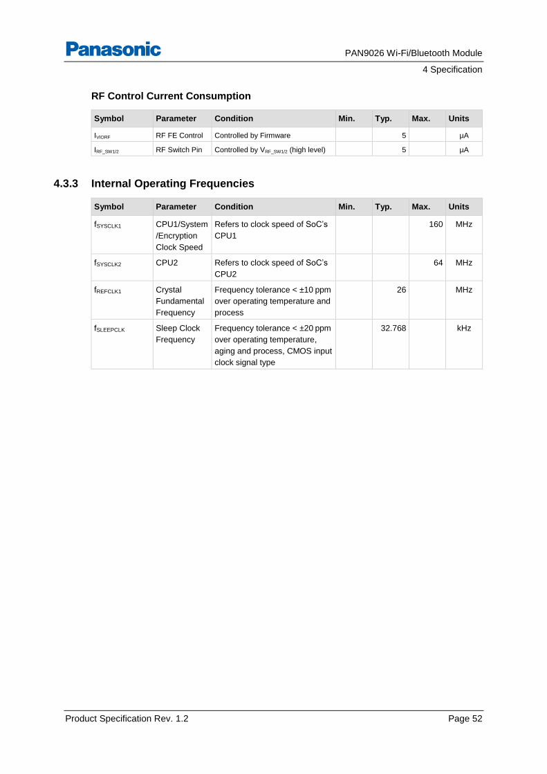
PAN9026 Wi-Fi/Bluetooth Module
4 Specification
Product Specification Rev. 1.2 Page 52
RF Control Current Consumption
Symbol Parameter Condition Min. Typ. Max. Units
IVIORF RF FE Control Controlled by Firmware 5 µA
IRF_SW1/2 RF Switch Pin Controlled by VRF_SW1/2 (high level) 5 µA
4.3.3 Internal Operating Frequencies
Symbol Parameter Condition Min. Typ. Max. Units
fSYSCLK1 CPU1/System
/Encryption
Clock Speed
Refers to clock speed of SoC’s
CPU1
160 MHz
fSYSCLK2 CPU2 Refers to clock speed of SoC’s
CPU2
64 MHz
fREFCLK1 Crystal
Fundamental
Frequency
Frequency tolerance < ±10 ppm
over operating temperature and
process
26 MHz
fSLEEPCLK Sleep Clock
Frequency
Frequency tolerance < ±20 ppm
over operating temperature,
aging and process, CMOS input
clock signal type
32.768 kHz
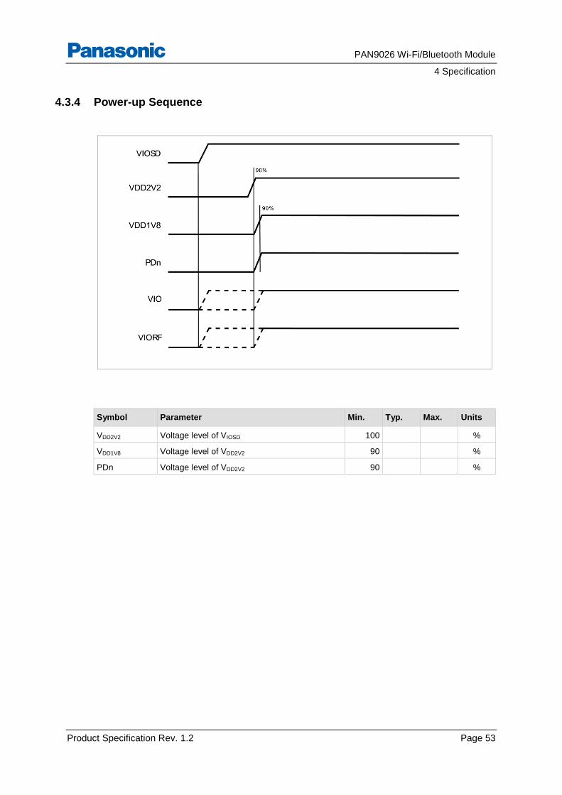
PAN9026 Wi-Fi/Bluetooth Module
4 Specification
Product Specification Rev. 1.2 Page 53
4.3.4 Power-up Sequence
Symbol Parameter Min. Typ. Max. Units
VDD2V2 Voltage level of VIOSD 100 %
VDD1V8 Voltage level of VDD2V2 90 %
PDn Voltage level of VDD2V2 90 %
PAN9026 Wi-Fi/Bluetooth Module
4 Specification
Product Specification Rev. 1.2 Page 54
4.3.5 Host Interface
4.3.5.1 SDIO Interface
The SDIO Interface pins are powered from the VIOSD voltage supply with either 3.3 V or 1.8 V. The SDIO electrical specifications are identical for the 1-bit and 4-bit SDIO modes.
For the DC specification please refer to 4.3.1 Digital Pin Characteristics.
SDIO Timing Data: Default and High-Speed Modes (VIOSD 3.3 V)17,18
Symbol Parameter Condition Min. Typ. Max. Units
fPP Clock Frequency Normal 0 25 MHz
High-speed 0 50 MHz
TWL Clock Low Time Normal 10 ns
High-speed 7 ns
TWH Clock High Time
Normal 10 ns
High-speed 7 ns
TISU Input Setup Time Normal 5 ns
High-speed 6 ns
TIH Input Hold Time Normal 5 ns
High-speed 2 ns
TODLY Output Delay Time Normal 14 ns
CL 40 Pf (1 Card) High-speed 14 ns
TOH Output Hold Time High-speed 2.5 ns
17
For SDIO 2.0 running at 50 MHz clock frequency, a supply voltage VIOSD of 1.8 V is recommended.
18 For SDIO 2.0 running at 25 MHz clock frequency, either 1.8 V or 3.3 V can be used.
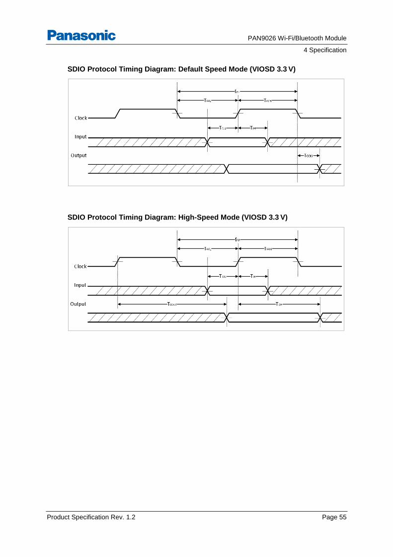
PAN9026 Wi-Fi/Bluetooth Module
4 Specification
Product Specification Rev. 1.2 Page 55
SDIO Protocol Timing Diagram: Default Speed Mode (VIOSD 3.3 V)
SDIO Protocol Timing Diagram: High-Speed Mode (VIOSD 3.3 V)
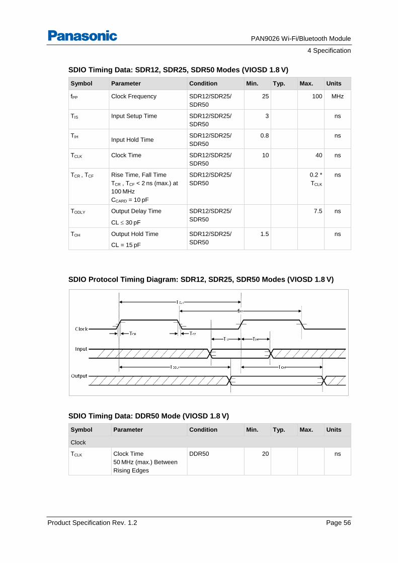
PAN9026 Wi-Fi/Bluetooth Module
4 Specification
Product Specification Rev. 1.2 Page 56
SDIO Timing Data: SDR12, SDR25, SDR50 Modes (VIOSD 1.8 V)
Symbol Parameter Condition Min. Typ. Max. Units
fPP Clock Frequency SDR12/SDR25/
SDR50
25 100 MHz
TIS Input Setup Time SDR12/SDR25/
SDR50
3 ns
TIH Input Hold Time
SDR12/SDR25/
SDR50
0.8 ns
TCLK Clock Time SDR12/SDR25/
SDR50
10 40 ns
TCR , TCF Rise Time, Fall Time
TCR , TCF < 2 ns (max.) at
100 MHz
CCARD = 10 pF
SDR12/SDR25/
SDR50
0.2 *
TCLK
ns
TODLY Output Delay Time
CL 30 pF
SDR12/SDR25/
SDR50
7.5 ns
TOH Output Hold Time
CL = 15 pF
SDR12/SDR25/
SDR50
1.5 ns
SDIO Protocol Timing Diagram: SDR12, SDR25, SDR50 Modes (VIOSD 1.8 V)
SDIO Timing Data: DDR50 Mode (VIOSD 1.8 V)
Symbol Parameter Condition Min. Typ. Max. Units
Clock
TCLK Clock Time
50 MHz (max.) Between
Rising Edges
DDR50 20 ns
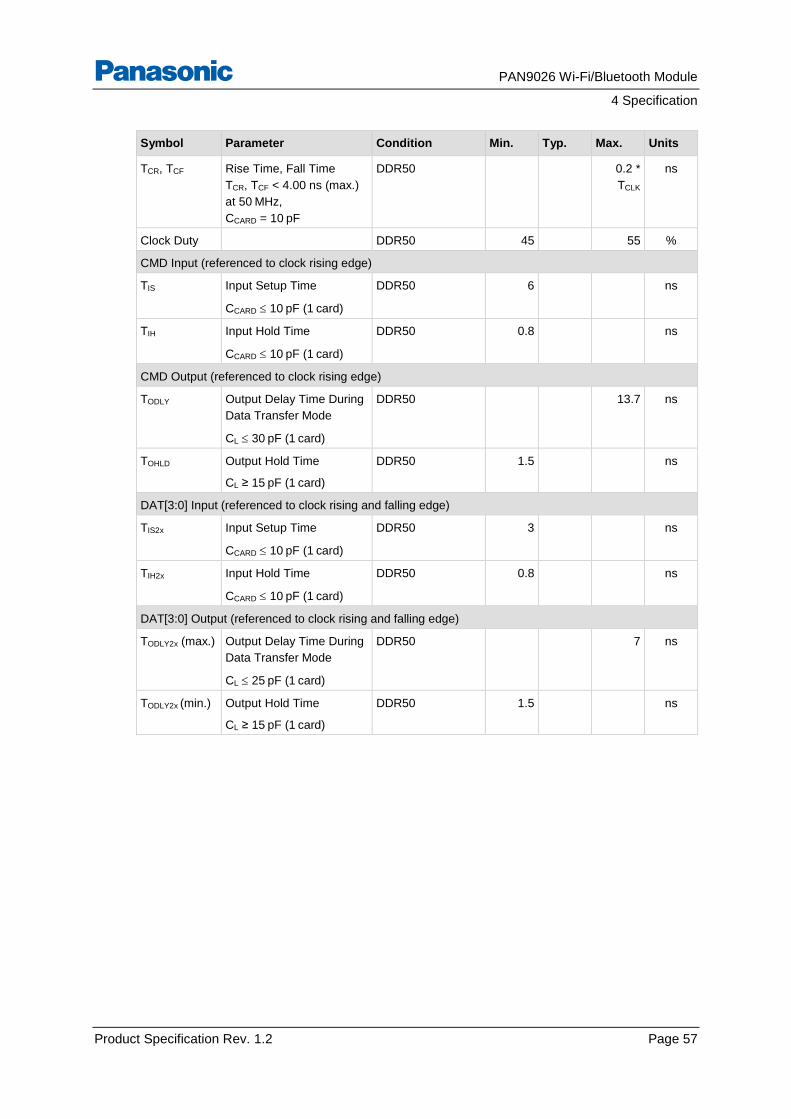
PAN9026 Wi-Fi/Bluetooth Module
4 Specification
Product Specification Rev. 1.2 Page 57
Symbol Parameter Condition Min. Typ. Max. Units
TCR, TCF Rise Time, Fall Time
TCR, TCF < 4.00 ns (max.)
at 50 MHz,
CCARD = 10 pF
DDR50 0.2 *
TCLK
ns
Clock Duty DDR50 45 55 %
CMD Input (referenced to clock rising edge)
TIS Input Setup Time
CCARD 10 pF (1 card)
DDR50 6 ns
TIH Input Hold Time
CCARD 10 pF (1 card)
DDR50 0.8 ns
CMD Output (referenced to clock rising edge)
TODLY Output Delay Time During
Data Transfer Mode
CL 30 pF (1 card)
DDR50 13.7 ns
TOHLD Output Hold Time
CL ≥ 15 pF (1 card)
DDR50 1.5 ns
DAT[3:0] Input (referenced to clock rising and falling edge)
TIS2x Input Setup Time
CCARD 10 pF (1 card)
DDR50 3 ns
TIH2x Input Hold Time
CCARD 10 pF (1 card)
DDR50 0.8 ns
DAT[3:0] Output (referenced to clock rising and falling edge)
TODLY2x (max.) Output Delay Time During
Data Transfer Mode
CL 25 pF (1 card)
DDR50 7 ns
TODLY2x (min.) Output Hold Time
CL ≥ 15 pF (1 card)
DDR50 1.5 ns
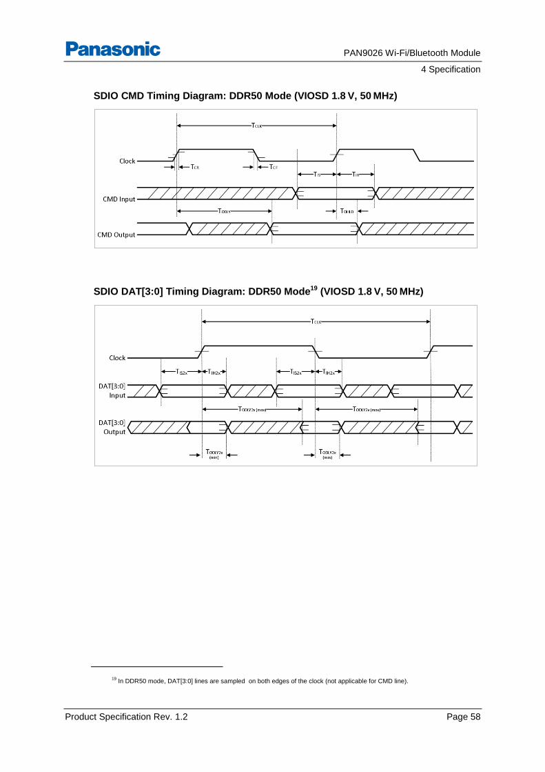
PAN9026 Wi-Fi/Bluetooth Module
4 Specification
Product Specification Rev. 1.2 Page 58
SDIO CMD Timing Diagram: DDR50 Mode (VIOSD 1.8 V, 50 MHz)
SDIO DAT[3:0] Timing Diagram: DDR50 Mode19 (VIOSD 1.8 V, 50 MHz)
19
In DDR50 mode, DAT[3:0] lines are sampled on both edges of the clock (not applicable for CMD line).
PAN9026 Wi-Fi/Bluetooth Module
4 Specification
Product Specification Rev. 1.2 Page 59
4.3.5.2 High-Speed UART Interface
The High-Speed UART Interface pins are powered from the VIO voltage supply with 1.8 V.
For the DC specification please refer to 4.3.1 Digital Pin Characteristics.
The UART interface operation includes:
• Support data input/output operations for peripheral devices connected through a standard UART interface
• 4-wire data transfer (RXD, TXD, RTS, CTS)
• Programmable baud rate (1 200 bps to 4 Mbps)
• Data format (LSB first)
• Data bit: 5 bit to 8 bit
• Parity bit: 0 bit to 4 bit
• Stop bit: 1 bit to 2 bit
Interface Signals
Pin No. Signal Name Specification
Name
Type Description
F3 UART_SOUT TXD
Host Controller
Interface (HCI)
Transmit data output
F4 UART_SIN RXD Receive data input
F5 UART_RTS RTS Request to send (active low)
G5 UART_CTS CTS Clear to send (active low)
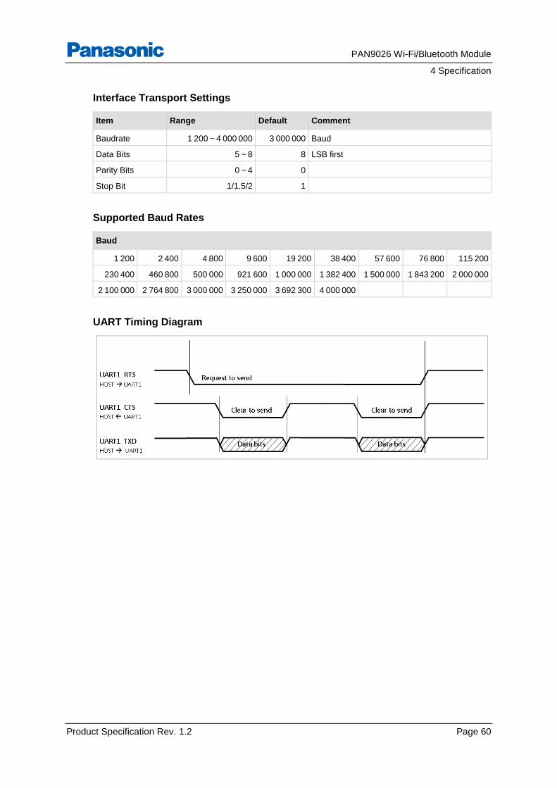
PAN9026 Wi-Fi/Bluetooth Module
4 Specification
Product Specification Rev. 1.2 Page 60
Interface Transport Settings
Item Range Default Comment
Baudrate 1 200 ~ 4 000 000 3 000 000 Baud
Data Bits 5 ~ 8 8 LSB first
Parity Bits 0 ~ 4 0
Stop Bit 1/1.5/2 1
Supported Baud Rates
Baud
1 200 2 400 4 800 9 600 19 200 38 400 57 600 76 800 115 200
230 400 460 800 500 000 921 600 1 000 000 1 382 400 1 500 000 1 843 200 2 000 000
2 100 000 2 764 800 3 000 000 3 250 000 3 692 300 4 000 000
UART Timing Diagram
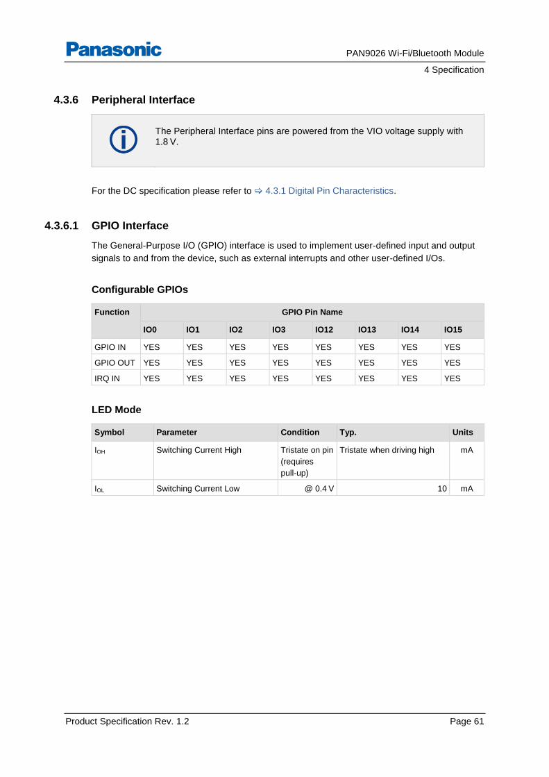
PAN9026 Wi-Fi/Bluetooth Module
4 Specification
Product Specification Rev. 1.2 Page 61
4.3.6 Peripheral Interface
The Peripheral Interface pins are powered from the VIO voltage supply with 1.8 V.
For the DC specification please refer to 4.3.1 Digital Pin Characteristics.
4.3.6.1 GPIO Interface
The General-Purpose I/O (GPIO) interface is used to implement user-defined input and output
signals to and from the device, such as external interrupts and other user-defined I/Os.
Configurable GPIOs
Function GPIO Pin Name
IO0 IO1 IO2 IO3 IO12 IO13 IO14 IO15
GPIO IN YES YES YES YES YES YES YES YES
GPIO OUT YES YES YES YES YES YES YES YES
IRQ IN YES YES YES YES YES YES YES YES
LED Mode
Symbol Parameter Condition Typ. Units
IOH Switching Current High Tristate on pin
(requires
pull-up)
Tristate when driving high mA
IOL Switching Current Low @ 0.4 V 10 mA
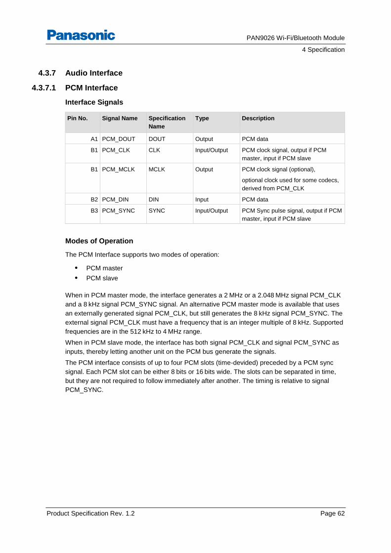
PAN9026 Wi-Fi/Bluetooth Module
4 Specification
Product Specification Rev. 1.2 Page 62
4.3.7 Audio Interface
4.3.7.1 PCM Interface
Interface Signals
Pin No. Signal Name Specification
Name
Type Description
A1 PCM_DOUT DOUT Output PCM data
B1 PCM_CLK CLK Input/Output PCM clock signal, output if PCM
master, input if PCM slave
B1 PCM_MCLK MCLK Output PCM clock signal (optional),
optional clock used for some codecs,
derived from PCM_CLK
B2 PCM_DIN DIN Input PCM data
B3 PCM_SYNC SYNC Input/Output PCM Sync pulse signal, output if PCM
master, input if PCM slave
Modes of Operation
The PCM Interface supports two modes of operation:
• PCM master
• PCM slave
When in PCM master mode, the interface generates a 2 MHz or a 2.048 MHz signal PCM_CLK
and a 8 kHz signal PCM_SYNC signal. An alternative PCM master mode is available that uses
an externally generated signal PCM_CLK, but still generates the 8 kHz signal PCM_SYNC. The
external signal PCM_CLK must have a frequency that is an integer multiple of 8 kHz. Supported
frequencies are in the 512 kHz to 4 MHz range.
When in PCM slave mode, the interface has both signal PCM_CLK and signal PCM_SYNC as
inputs, thereby letting another unit on the PCM bus generate the signals.
The PCM interface consists of up to four PCM slots (time-devided) preceded by a PCM sync
signal. Each PCM slot can be either 8 bits or 16 bits wide. The slots can be separated in time,
but they are not required to follow immediately after another. The timing is relative to signal
PCM_SYNC.
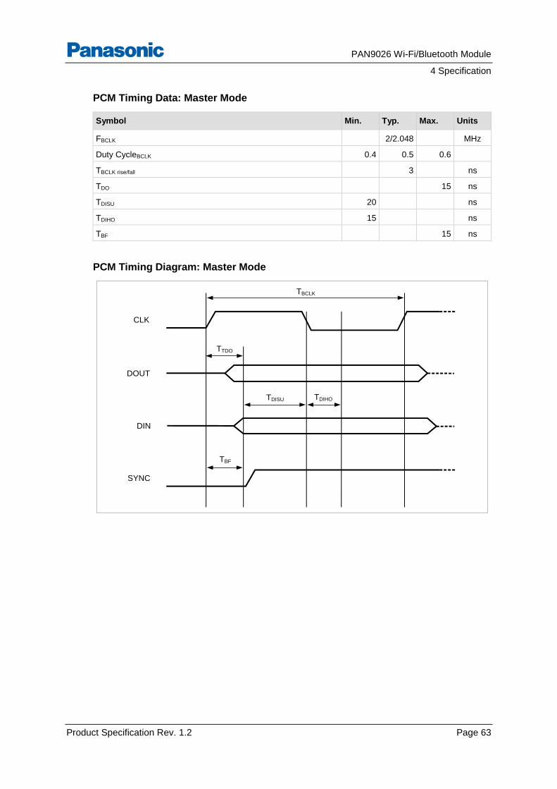
PAN9026 Wi-Fi/Bluetooth Module
4 Specification
Product Specification Rev. 1.2 Page 63
PCM Timing Data: Master Mode
Symbol Min. Typ. Max. Units
FBCLK 2/2.048 MHz
Duty CycleBCLK 0.4 0.5 0.6
TBCLK rise/fall 3 ns
TDO 15 ns
TDISU 20 ns
TDIHO 15 ns
TBF 15 ns
PCM Timing Diagram: Master Mode
CLK
DOUT
DIN
SYNC
TBF
TTDO
TBCLK
TDISU TDIHO
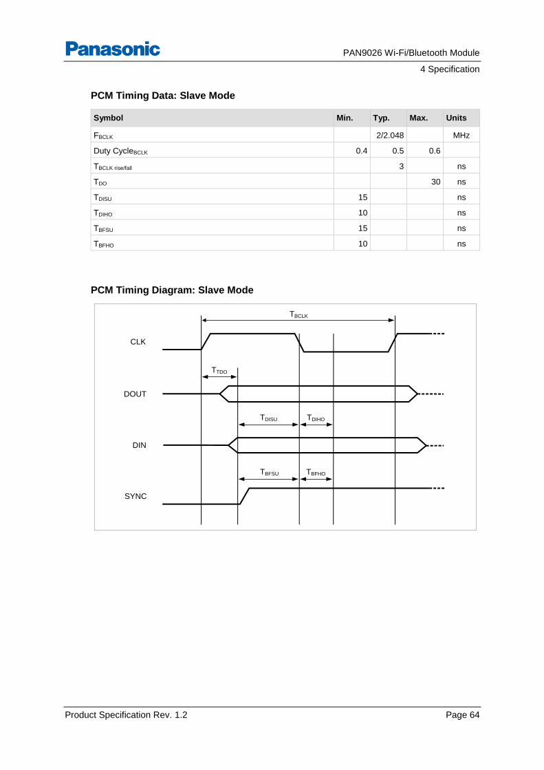
PAN9026 Wi-Fi/Bluetooth Module
4 Specification
Product Specification Rev. 1.2 Page 64
PCM Timing Data: Slave Mode
Symbol Min. Typ. Max. Units
FBCLK 2/2.048 MHz
Duty CycleBCLK 0.4 0.5 0.6
TBCLK rise/fall 3 ns
TDO 30 ns
TDISU 15 ns
TDIHO 10 ns
TBFSU 15 ns
TBFHO 10 ns
PCM Timing Diagram: Slave Mode
CLK
DOUT
DIN
SYNC
TBFSU
TTDO
TBCLK
TDISU TDIHO
TBFHO
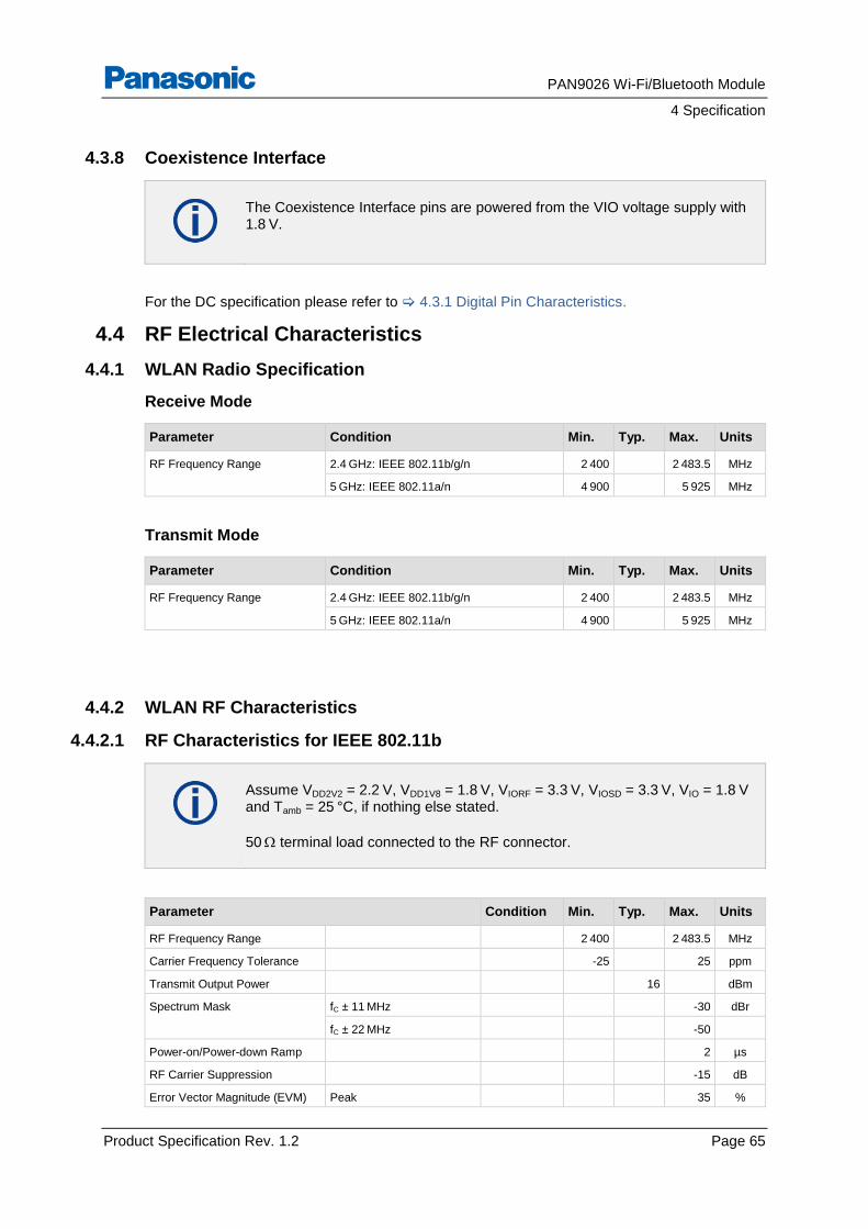
PAN9026 Wi-Fi/Bluetooth Module
4 Specification
Product Specification Rev. 1.2 Page 65
4.3.8 Coexistence Interface
The Coexistence Interface pins are powered from the VIO voltage supply with 1.8 V.
For the DC specification please refer to 4.3.1 Digital Pin Characteristics.
4.4 RF Electrical Characteristics
4.4.1 WLAN Radio Specification
Receive Mode
Parameter Condition Min. Typ. Max. Units
RF Frequency Range 2.4 GHz: IEEE 802.11b/g/n 2 400 2 483.5 MHz
5 GHz: IEEE 802.11a/n 4 900 5 925 MHz
Transmit Mode
Parameter Condition Min. Typ. Max. Units
RF Frequency Range 2.4 GHz: IEEE 802.11b/g/n 2 400 2 483.5 MHz
5 GHz: IEEE 802.11a/n 4 900 5 925 MHz
4.4.2 WLAN RF Characteristics
4.4.2.1 RF Characteristics for IEEE 802.11b
Assume VDD2V2 = 2.2 V, VDD1V8 = 1.8 V, VIORF = 3.3 V, VIOSD = 3.3 V, VIO = 1.8 V and Tamb = 25 °C, if nothing else stated.
50 terminal load connected to the RF connector.
Parameter Condition Min. Typ. Max. Units
RF Frequency Range 2 400 2 483.5 MHz
Carrier Frequency Tolerance -25 25 ppm
Transmit Output Power 16 dBm
Spectrum Mask fC ± 11 MHz -30 dBr
fC ± 22 MHz -50
Power-on/Power-down Ramp 2 µs
RF Carrier Suppression -15 dB
Error Vector Magnitude (EVM) Peak 35 %
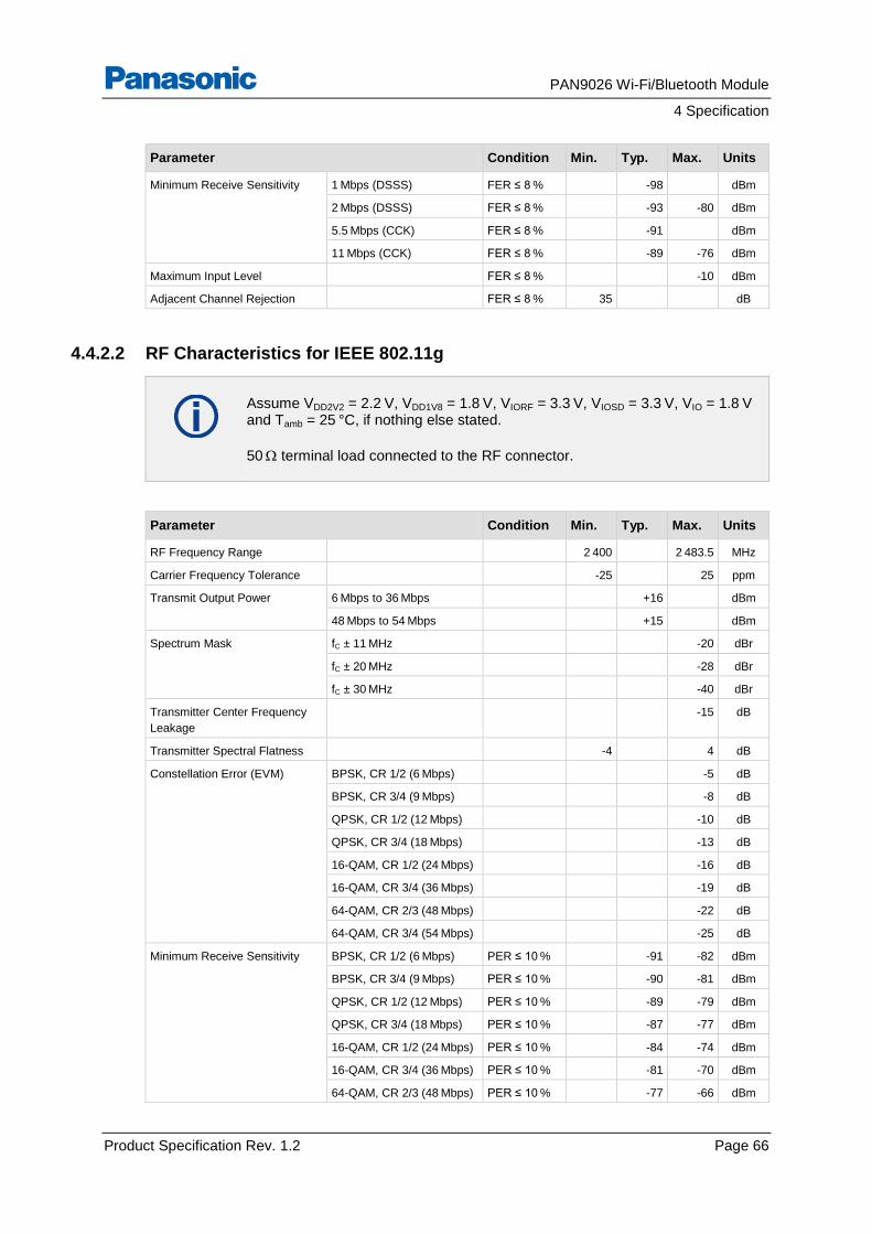
PAN9026 Wi-Fi/Bluetooth Module
4 Specification
Product Specification Rev. 1.2 Page 66
Parameter Condition Min. Typ. Max. Units
Minimum Receive Sensitivity 1 Mbps (DSSS) FER ≤ 8 % -98 dBm
2 Mbps (DSSS) FER ≤ 8 % -93 -80 dBm
5.5 Mbps (CCK) FER ≤ 8 % -91 dBm
11 Mbps (CCK) FER ≤ 8 % -89 -76 dBm
Maximum Input Level FER ≤ 8 % -10 dBm
Adjacent Channel Rejection FER ≤ 8 % 35 dB
4.4.2.2 RF Characteristics for IEEE 802.11g
Assume VDD2V2 = 2.2 V, VDD1V8 = 1.8 V, VIORF = 3.3 V, VIOSD = 3.3 V, VIO = 1.8 V and Tamb = 25 °C, if nothing else stated.
50 terminal load connected to the RF connector.
Parameter Condition Min. Typ. Max. Units
RF Frequency Range 2 400 2 483.5 MHz
Carrier Frequency Tolerance -25 25 ppm
Transmit Output Power 6 Mbps to 36 Mbps +16 dBm
48 Mbps to 54 Mbps +15 dBm
Spectrum Mask fC ± 11 MHz -20 dBr
fC ± 20 MHz -28 dBr
fC ± 30 MHz -40 dBr
Transmitter Center Frequency
Leakage
-15 dB
Transmitter Spectral Flatness -4 4 dB
Constellation Error (EVM) BPSK, CR 1/2 (6 Mbps) -5 dB
BPSK, CR 3/4 (9 Mbps) -8 dB
QPSK, CR 1/2 (12 Mbps) -10 dB
QPSK, CR 3/4 (18 Mbps) -13 dB
16-QAM, CR 1/2 (24 Mbps) -16 dB
16-QAM, CR 3/4 (36 Mbps) -19 dB
64-QAM, CR 2/3 (48 Mbps) -22 dB
64-QAM, CR 3/4 (54 Mbps) -25 dB
Minimum Receive Sensitivity BPSK, CR 1/2 (6 Mbps) PER ≤ 10 % -91 -82 dBm
BPSK, CR 3/4 (9 Mbps) PER ≤ 10 % -90 -81 dBm
QPSK, CR 1/2 (12 Mbps) PER ≤ 10 % -89 -79 dBm
QPSK, CR 3/4 (18 Mbps) PER ≤ 10 % -87 -77 dBm
16-QAM, CR 1/2 (24 Mbps) PER ≤ 10 % -84 -74 dBm
16-QAM, CR 3/4 (36 Mbps) PER ≤ 10 % -81 -70 dBm
64-QAM, CR 2/3 (48 Mbps) PER ≤ 10 % -77 -66 dBm
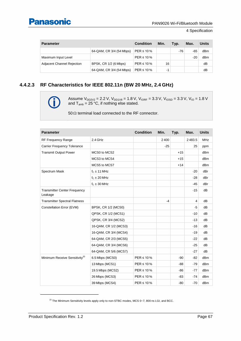
PAN9026 Wi-Fi/Bluetooth Module
4 Specification
Product Specification Rev. 1.2 Page 67
Parameter Condition Min. Typ. Max. Units
64-QAM, CR 3/4 (54 Mbps) PER ≤ 10 % -76 -65 dBm
Maximum Input Level PER ≤ 10 % -20 dBm
Adjacent Channel Rejection BPSK, CR 1/2 (6 Mbps) PER ≤ 10 % 16 dB
64-QAM, CR 3/4 (54 Mbps) PER ≤ 10 % -1 dB
4.4.2.3 RF Characteristics for IEEE 802.11n (BW 20 MHz, 2.4 GHz)
Assume VDD2V2 = 2.2 V, VDD1V8 = 1.8 V, VIORF = 3.3 V, VIOSD = 3.3 V, VIO = 1.8 V and Tamb = 25 °C, if nothing else stated.
50 terminal load connected to the RF connector.
Parameter Condition Min. Typ. Max. Units
RF Frequency Range 2.4 GHz 2 400 2 483.5 MHz
Carrier Frequency Tolerance -25 25 ppm
Transmit Output Power
MCS0 to MCS2 +15 dBm
MCS3 to MCS4 +15 dBm
MCS5 to MCS7 +14 dBm
Spectrum Mask
fC ± 11 MHz -20 dBr
fC ± 20 MHz -28 dBr
fC ± 30 MHz -45 dBr
Transmitter Center Frequency
Leakage
-15 dB
Transmitter Spectral Flatness -4 4 dB
Constellation Error (EVM) BPSK, CR 1/2 (MCS0) -5 dB
QPSK, CR 1/2 (MCS1) -10 dB
QPSK, CR 3/4 (MCS2) -13 dB
16-QAM, CR 1/2 (MCS3) -16 dB
16-QAM, CR 3/4 (MCS4) -19 dB
64-QAM, CR 2/3 (MCS5) -22 dB
64-QAM, CR 3/4 (MCS6) -25 dB
64-QAM, CR 5/6 (MCS7) -27 dB
Minimum Receive Sensitivity20
6.5 Mbps (MCS0) PER ≤ 10 % -90 -82 dBm
13 Mbps (MCS1) PER ≤ 10 % -88 -79 dBm
19.5 Mbps (MCS2) PER ≤ 10 % -86 -77 dBm
26 Mbps (MCS3) PER ≤ 10 % -83 -74 dBm
39 Mbps (MCS4) PER ≤ 10 % -80 -70 dBm
20
The Minimum Sensitivity levels apply only to non-STBC modes, MCS 0~7, 800 ns LGI, and BCC.
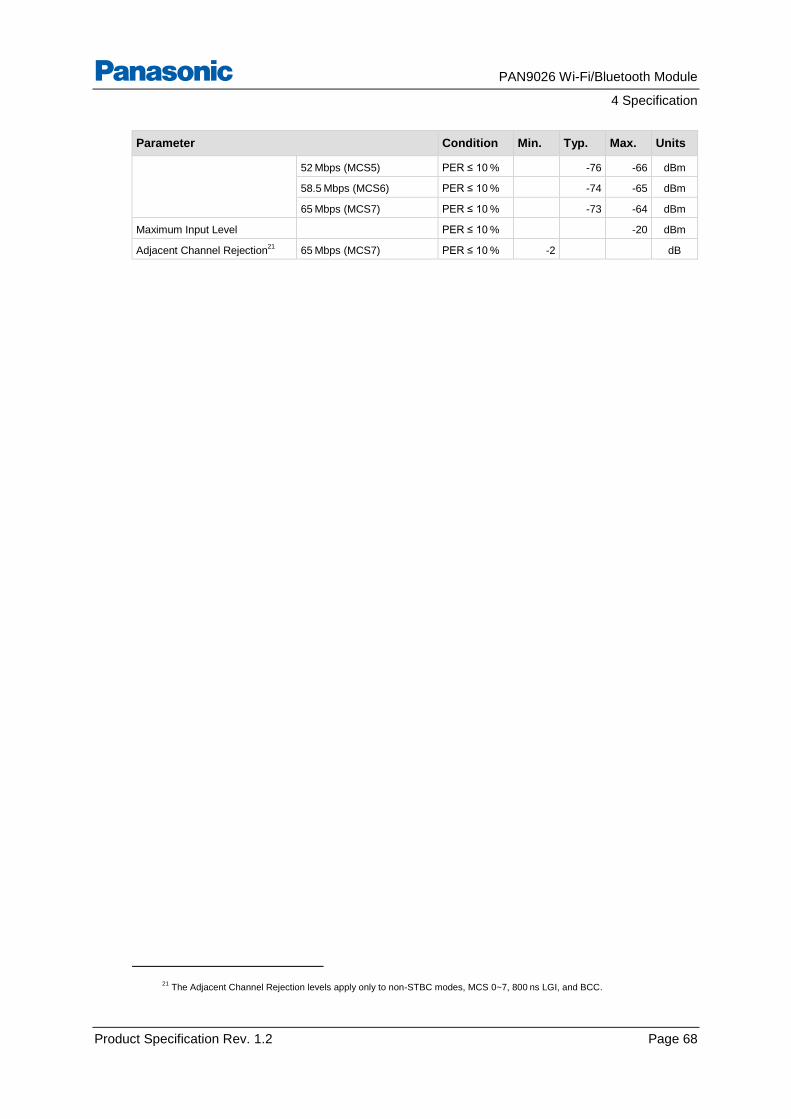
PAN9026 Wi-Fi/Bluetooth Module
4 Specification
Product Specification Rev. 1.2 Page 68
Parameter Condition Min. Typ. Max. Units
52 Mbps (MCS5) PER ≤ 10 % -76 -66 dBm
58.5 Mbps (MCS6) PER ≤ 10 % -74 -65 dBm
65 Mbps (MCS7) PER ≤ 10 % -73 -64 dBm
Maximum Input Level PER ≤ 10 % -20 dBm
Adjacent Channel Rejection21
65 Mbps (MCS7) PER ≤ 10 % -2 dB
21
The Adjacent Channel Rejection levels apply only to non-STBC modes, MCS 0~7, 800 ns LGI, and BCC.
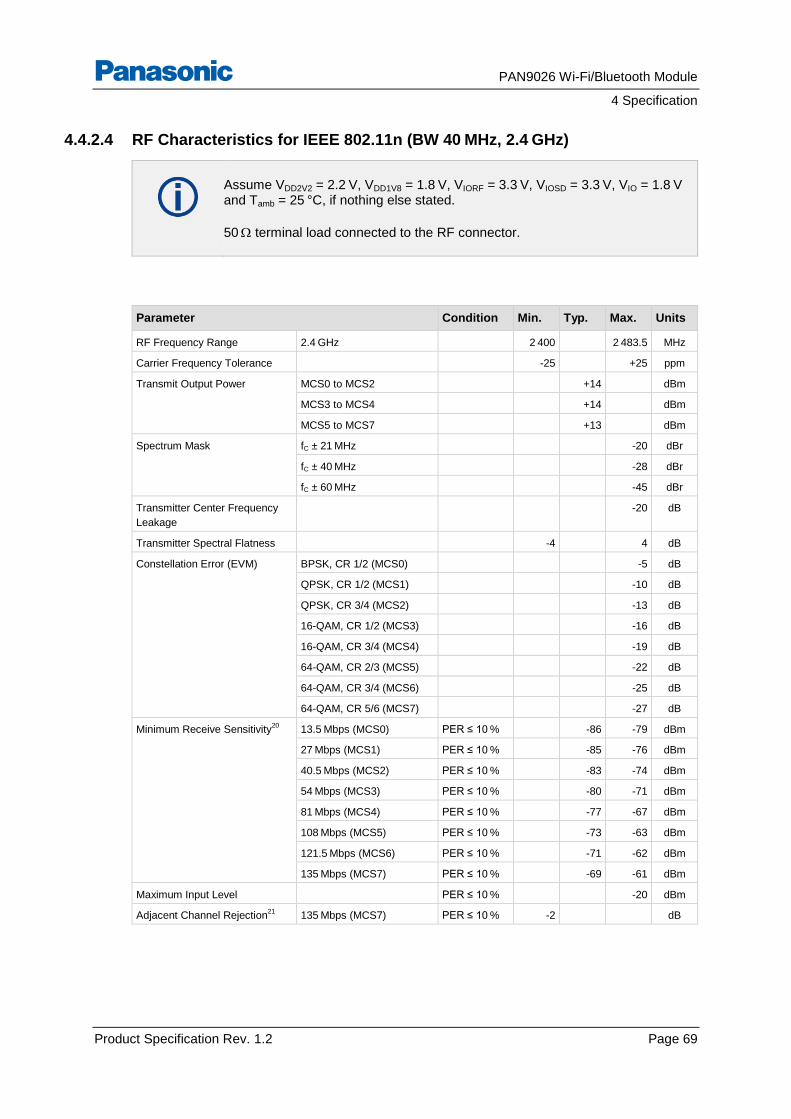
PAN9026 Wi-Fi/Bluetooth Module
4 Specification
Product Specification Rev. 1.2 Page 69
4.4.2.4 RF Characteristics for IEEE 802.11n (BW 40 MHz, 2.4 GHz)
Assume VDD2V2 = 2.2 V, VDD1V8 = 1.8 V, VIORF = 3.3 V, VIOSD = 3.3 V, VIO = 1.8 V and Tamb = 25 °C, if nothing else stated.
50 terminal load connected to the RF connector.
Parameter Condition Min. Typ. Max. Units
RF Frequency Range 2.4 GHz 2 400 2 483.5 MHz
Carrier Frequency Tolerance -25 +25 ppm
Transmit Output Power
MCS0 to MCS2 +14 dBm
MCS3 to MCS4 +14 dBm
MCS5 to MCS7 +13 dBm
Spectrum Mask
fC ± 21 MHz -20 dBr
fC ± 40 MHz -28 dBr
fC ± 60 MHz -45 dBr
Transmitter Center Frequency
Leakage
-20 dB
Transmitter Spectral Flatness -4 4 dB
Constellation Error (EVM)
BPSK, CR 1/2 (MCS0) -5 dB
QPSK, CR 1/2 (MCS1) -10 dB
QPSK, CR 3/4 (MCS2) -13 dB
16-QAM, CR 1/2 (MCS3) -16 dB
16-QAM, CR 3/4 (MCS4) -19 dB
64-QAM, CR 2/3 (MCS5) -22 dB
64-QAM, CR 3/4 (MCS6) -25 dB
64-QAM, CR 5/6 (MCS7) -27 dB
Minimum Receive Sensitivity20
13.5 Mbps (MCS0) PER ≤ 10 % -86 -79 dBm
27 Mbps (MCS1) PER ≤ 10 % -85 -76 dBm
40.5 Mbps (MCS2) PER ≤ 10 % -83 -74 dBm
54 Mbps (MCS3) PER ≤ 10 % -80 -71 dBm
81 Mbps (MCS4) PER ≤ 10 % -77 -67 dBm
108 Mbps (MCS5) PER ≤ 10 % -73 -63 dBm
121.5 Mbps (MCS6) PER ≤ 10 % -71 -62 dBm
135 Mbps (MCS7) PER ≤ 10 % -69 -61 dBm
Maximum Input Level PER ≤ 10 % -20 dBm
Adjacent Channel Rejection21
135 Mbps (MCS7) PER ≤ 10 % -2 dB
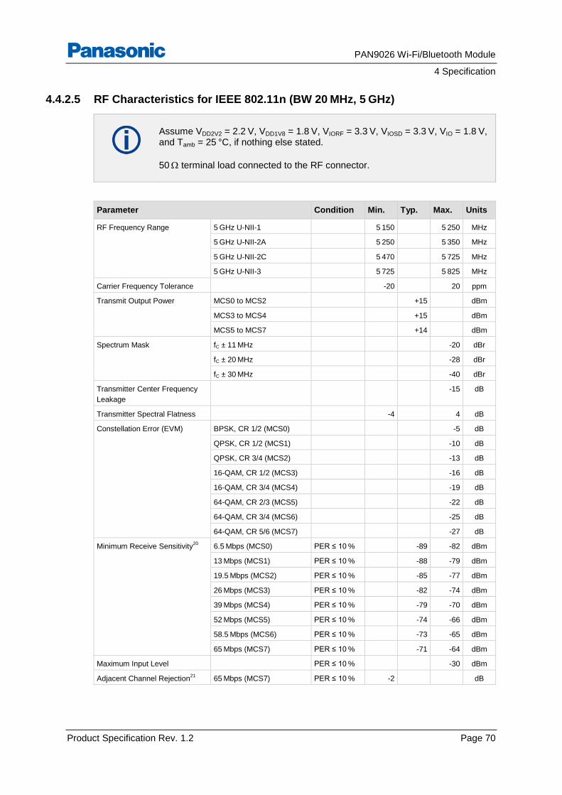
PAN9026 Wi-Fi/Bluetooth Module
4 Specification
Product Specification Rev. 1.2 Page 70
4.4.2.5 RF Characteristics for IEEE 802.11n (BW 20 MHz, 5 GHz)
Assume VDD2V2 = 2.2 V, VDD1V8 = 1.8 V, VIORF = 3.3 V, VIOSD = 3.3 V, VIO = 1.8 V, and Tamb = 25 °C, if nothing else stated.
50 terminal load connected to the RF connector.
Parameter Condition Min. Typ. Max. Units
RF Frequency Range 5 GHz U-NII-1 5 150 5 250 MHz
5 GHz U-NII-2A 5 250 5 350 MHz
5 GHz U-NII-2C 5 470 5 725 MHz
5 GHz U-NII-3 5 725 5 825 MHz
Carrier Frequency Tolerance -20 20 ppm
Transmit Output Power
MCS0 to MCS2 +15 dBm
MCS3 to MCS4 +15 dBm
MCS5 to MCS7 +14 dBm
Spectrum Mask
fC ± 11 MHz -20 dBr
fC ± 20 MHz -28 dBr
fC ± 30 MHz -40 dBr
Transmitter Center Frequency
Leakage
-15 dB
Transmitter Spectral Flatness -4 4 dB
Constellation Error (EVM) BPSK, CR 1/2 (MCS0) -5 dB
QPSK, CR 1/2 (MCS1) -10 dB
QPSK, CR 3/4 (MCS2) -13 dB
16-QAM, CR 1/2 (MCS3) -16 dB
16-QAM, CR 3/4 (MCS4) -19 dB
64-QAM, CR 2/3 (MCS5) -22 dB
64-QAM, CR 3/4 (MCS6) -25 dB
64-QAM, CR 5/6 (MCS7) -27 dB
Minimum Receive Sensitivity20
6.5 Mbps (MCS0) PER ≤ 10 % -89 -82 dBm
13 Mbps (MCS1) PER ≤ 10 % -88 -79 dBm
19.5 Mbps (MCS2) PER ≤ 10 % -85 -77 dBm
26 Mbps (MCS3) PER ≤ 10 % -82 -74 dBm
39 Mbps (MCS4) PER ≤ 10 % -79 -70 dBm
52 Mbps (MCS5) PER ≤ 10 % -74 -66 dBm
58.5 Mbps (MCS6) PER ≤ 10 % -73 -65 dBm
65 Mbps (MCS7) PER ≤ 10 % -71 -64 dBm
Maximum Input Level PER ≤ 10 % -30 dBm
Adjacent Channel Rejection21
65 Mbps (MCS7) PER ≤ 10 % -2 dB
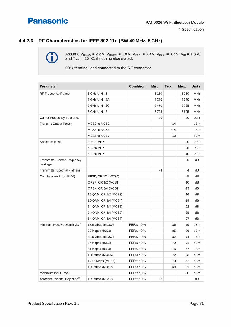
PAN9026 Wi-Fi/Bluetooth Module
4 Specification
Product Specification Rev. 1.2 Page 71
4.4.2.6 RF Characteristics for IEEE 802.11n (BW 40 MHz, 5 GHz)
Assume VDD2V2 = 2.2 V, VDD1V8 = 1.8 V, VIORF = 3.3 V, VIOSD = 3.3 V, VIO = 1.8 V, and Tamb = 25 °C, if nothing else stated.
50 terminal load connected to the RF connector.
Parameter Condition Min. Typ. Max. Units
RF Frequency Range 5 GHz U-NII-1 5 150 5 250 MHz
5 GHz U-NII-2A 5 250 5 350 MHz
5 GHz U-NII-2C 5 470 5 725 MHz
5 GHz U-NII-3 5 725 5 825 MHz
Carrier Frequency Tolerance -20 20 ppm
Transmit Output Power
MCS0 to MCS2 +14 dBm
MCS3 to MCS4 +14 dBm
MCS5 to MCS7 +13 dBm
Spectrum Mask
fC ± 21 MHz -20 dBr
fC ± 40 MHz -28 dBr
fC ± 60 MHz -40 dBr
Transmitter Center Frequency
Leakage
-20 dB
Transmitter Spectral Flatness -4 4 dB
Constellation Error (EVM)
BPSK, CR 1/2 (MCS0) -5 dB
QPSK, CR 1/2 (MCS1) -10 dB
QPSK, CR 3/4 (MCS2) -13 dB
16-QAM, CR 1/2 (MCS3) -16 dB
16-QAM, CR 3/4 (MCS4) -19 dB
64-QAM, CR 2/3 (MCS5) -22 dB
64-QAM, CR 3/4 (MCS6) -25 dB
64-QAM, CR 5/6 (MCS7) -27 dB
Minimum Receive Sensitivity20
13.5 Mbps (MCS0) PER ≤ 10 % -86 -79 dBm
27 Mbps (MCS1) PER ≤ 10 % -85 -76 dBm
40.5 Mbps (MCS2) PER ≤ 10 % -82 -74 dBm
54 Mbps (MCS3) PER ≤ 10 % -79 -71 dBm
81 Mbps (MCS4) PER ≤ 10 % -76 -67 dBm
108 Mbps (MCS5) PER ≤ 10 % -72 -63 dBm
121.5 Mbps (MCS6) PER ≤ 10 % -70 -62 dBm
135 Mbps (MCS7) PER ≤ 10 % -69 -61 dBm
Maximum Input Level PER ≤ 10 % -30 dBm
Adjacent Channel Rejection21
135 Mbps (MCS7) PER ≤ 10 % -2 dB
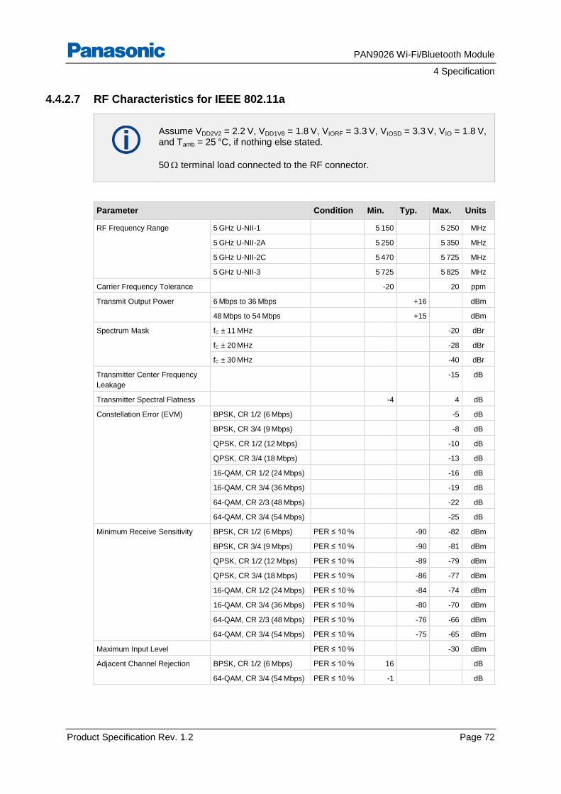
PAN9026 Wi-Fi/Bluetooth Module
4 Specification
Product Specification Rev. 1.2 Page 72
4.4.2.7 RF Characteristics for IEEE 802.11a
Assume VDD2V2 = 2.2 V, VDD1V8 = 1.8 V, VIORF = 3.3 V, VIOSD = 3.3 V, VIO = 1.8 V, and Tamb = 25 °C, if nothing else stated.
50 terminal load connected to the RF connector.
Parameter Condition Min. Typ. Max. Units
RF Frequency Range 5 GHz U-NII-1 5 150 5 250 MHz
5 GHz U-NII-2A 5 250 5 350 MHz
5 GHz U-NII-2C 5 470 5 725 MHz
5 GHz U-NII-3 5 725 5 825 MHz
Carrier Frequency Tolerance -20 20 ppm
Transmit Output Power
6 Mbps to 36 Mbps +16 dBm
48 Mbps to 54 Mbps +15 dBm
Spectrum Mask
fC ± 11 MHz -20 dBr
fC ± 20 MHz -28 dBr
fC ± 30 MHz -40 dBr
Transmitter Center Frequency
Leakage
-15 dB
Transmitter Spectral Flatness -4 4 dB
Constellation Error (EVM)
BPSK, CR 1/2 (6 Mbps) -5 dB
BPSK, CR 3/4 (9 Mbps) -8 dB
QPSK, CR 1/2 (12 Mbps) -10 dB
QPSK, CR 3/4 (18 Mbps) -13 dB
16-QAM, CR 1/2 (24 Mbps) -16 dB
16-QAM, CR 3/4 (36 Mbps) -19 dB
64-QAM, CR 2/3 (48 Mbps) -22 dB
64-QAM, CR 3/4 (54 Mbps) -25 dB
Minimum Receive Sensitivity BPSK, CR 1/2 (6 Mbps) PER ≤ 10 % -90 -82 dBm
BPSK, CR 3/4 (9 Mbps) PER ≤ 10 % -90 -81 dBm
QPSK, CR 1/2 (12 Mbps) PER ≤ 10 % -89 -79 dBm
QPSK, CR 3/4 (18 Mbps) PER ≤ 10 % -86 -77 dBm
16-QAM, CR 1/2 (24 Mbps) PER ≤ 10 % -84 -74 dBm
16-QAM, CR 3/4 (36 Mbps) PER ≤ 10 % -80 -70 dBm
64-QAM, CR 2/3 (48 Mbps) PER ≤ 10 % -76 -66 dBm
64-QAM, CR 3/4 (54 Mbps) PER ≤ 10 % -75 -65 dBm
Maximum Input Level PER ≤ 10 % -30 dBm
Adjacent Channel Rejection BPSK, CR 1/2 (6 Mbps) PER ≤ 10 % 16 dB
64-QAM, CR 3/4 (54 Mbps) PER ≤ 10 % -1 dB
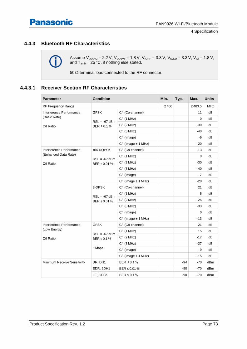
PAN9026 Wi-Fi/Bluetooth Module
4 Specification
Product Specification Rev. 1.2 Page 73
4.4.3 Bluetooth RF Characteristics
Assume VDD2V2 = 2.2 V, VDD1V8 = 1.8 V, VIORF = 3.3 V, VIOSD = 3.3 V, VIO = 1.8 V, and Tamb = 25 °C, if nothing else stated.
50 terminal load connected to the RF connector.
4.4.3.1 Receiver Section RF Characteristics
Parameter Condition Min. Typ. Max. Units
RF Frequency Range 2 400 2 483.5 MHz
Interference Performance
(Basic Rate)
C/I Ratio
GFSK
RSL = -67 dBm
BER ≤ 0.1 %
C/I (Co-channel) 11 dB
C/I (1 MHz) 0 dB
C/I (2 MHz) -30 dB
C/I (3 MHz) -40 dB
C/I (Image) -9 dB
C/I (Image ± 1 MHz) -20 dB
Interference Performance
(Enhanced Data Rate)
C/I Ratio
π/4-DQPSK
RSL = -67 dBm
BER ≤ 0.01 %
C/I (Co-channel) 13 dB
C/I (1 MHz) 0 dB
C/I (2 MHz) -30 dB
C/I (3 MHz) -40 dB
C/I (Image) -7 dB
C/I (Image ± 1 MHz) -20 dB
8-DPSK
RSL = -67 dBm
BER ≤ 0.01 %
C/I (Co-channel) 21 dB
C/I (1 MHz) 5 dB
C/I (2 MHz) -25 dB
C/I (3 MHz) -33 dB
C/I (Image) 0 dB
C/I (Image ± 1 MHz) -13 dB
Interference Performance
(Low Energy)
C/I Ratio
GFSK
RSL = -67 dBm
BER ≤ 0.1 %
1 Mbps
C/I (Co-channel) 21 dB
C/I (1 MHz) 15 dB
C/I (2 MHz) -17 dB
C/I (3 MHz) -27 dB
C/I (Image) -9 dB
C/I (Image ± 1 MHz) -15 dB
Minimum Receive Sensitivity BR, DH1 BER ≤ 0.1 % -94 -70 dBm
EDR, 2DH1 BER ≤ 0.01 % -90 -70 dBm
LE, GFSK BER ≤ 0.1 % -90 -70 dBm
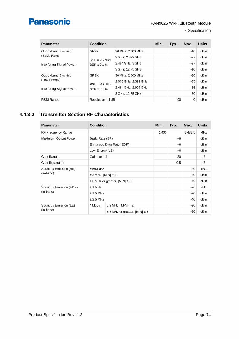
PAN9026 Wi-Fi/Bluetooth Module
4 Specification
Product Specification Rev. 1.2 Page 74
Parameter Condition Min. Typ. Max. Units
Out-of-band Blocking
(Basic Rate)
Interfering Signal Power
GFSK
RSL = -67 dBm
BER ≤ 0.1 %
30 MHz: 2 000 MHz -10 dBm
2 GHz: 2.399 GHz -27 dBm
2.484 GHz: 3 GHz -27 dBm
3 GHz: 12.75 GHz -10 dBm
Out-of-band Blocking
(Low Energy)
Interfering Signal Power
GFSK
RSL = -67 dBm
BER ≤ 0.1 %
30 MHz: 2 000 MHz -30 dBm
2.003 GHz: 2.399 GHz -35 dBm
2.484 GHz: 2.997 GHz -35 dBm
3 GHz: 12.75 GHz -30 dBm
RSSI Range Resolution = 1 dB -90 0 dBm
4.4.3.2 Transmitter Section RF Characteristics
Parameter Condition Min. Typ. Max. Units
RF Frequency Range 2 400 2 483.5 MHz
Maximum Output Power Basic Rate (BR) +8 dBm
Enhanced Data Rate (EDR) +6 dBm
Low Energy (LE) +6 dBm
Gain Range Gain control 30 dB
Gain Resolution 0.5 dB
Spurious Emission (BR)
(in-band)
± 500 kHz -20 dBc
± 2 MHz, |M-N| = 2 -20 dBm
± 3 MHz or greater, |M-N| ≥ 3 -40 dBm
Spurious Emission (EDR)
(in-band)
± 1 MHz -26 dBc
± 1.5 MHz -20 dBm
± 2.5 MHz -40 dBm
Spurious Emission (LE)
(in-band)
1 Mbps ± 2 MHz, |M-N| = 2 -20 dBm
± 3 MHz or greater, |M-N| ≥ 3 -30 dBm
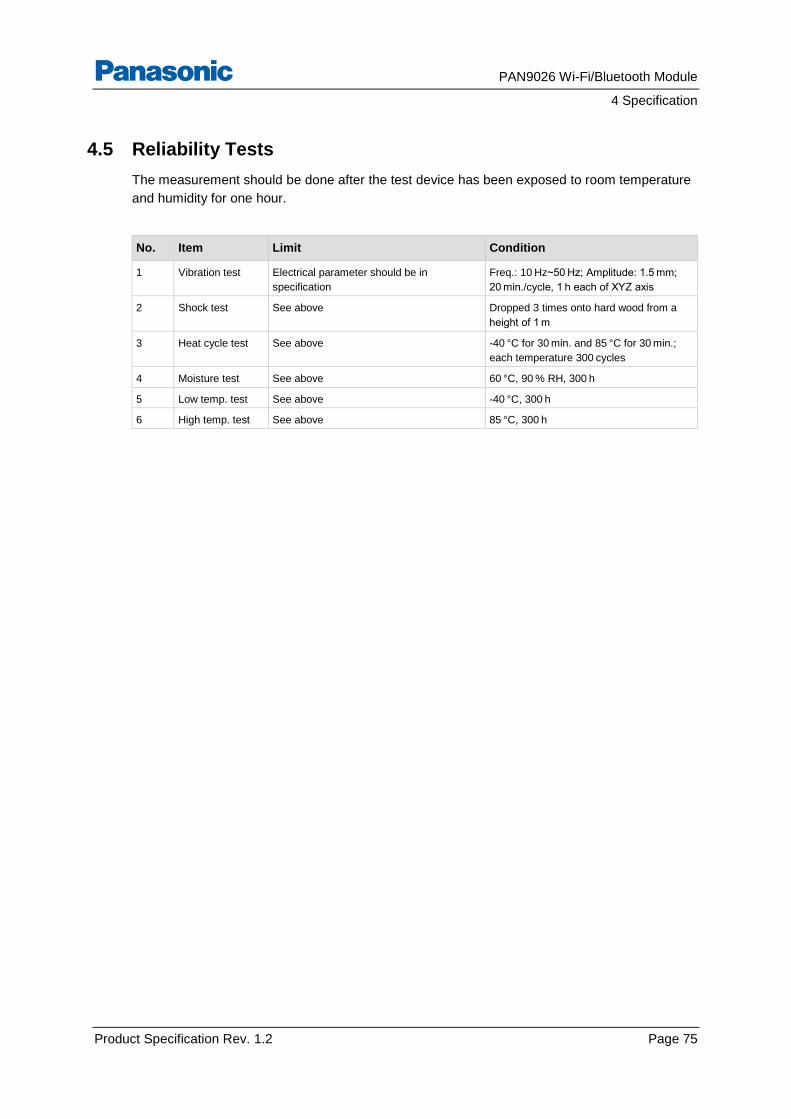
PAN9026 Wi-Fi/Bluetooth Module
4 Specification
Product Specification Rev. 1.2 Page 75
4.5 Reliability Tests
The measurement should be done after the test device has been exposed to room temperature
and humidity for one hour.
No. Item Limit Condition
1 Vibration test Electrical parameter should be in
specification
Freq.: 10 Hz~50 Hz; Amplitude: 1.5 mm;
20 min./cycle, 1 h each of XYZ axis
2 Shock test See above Dropped 3 times onto hard wood from a
height of 1 m
3 Heat cycle test See above -40 °C for 30 min. and 85 °C for 30 min.;
each temperature 300 cycles
4 Moisture test See above 60 °C, 90 % RH, 300 h
5 Low temp. test See above -40 °C, 300 h
6 High temp. test See above 85 °C, 300 h
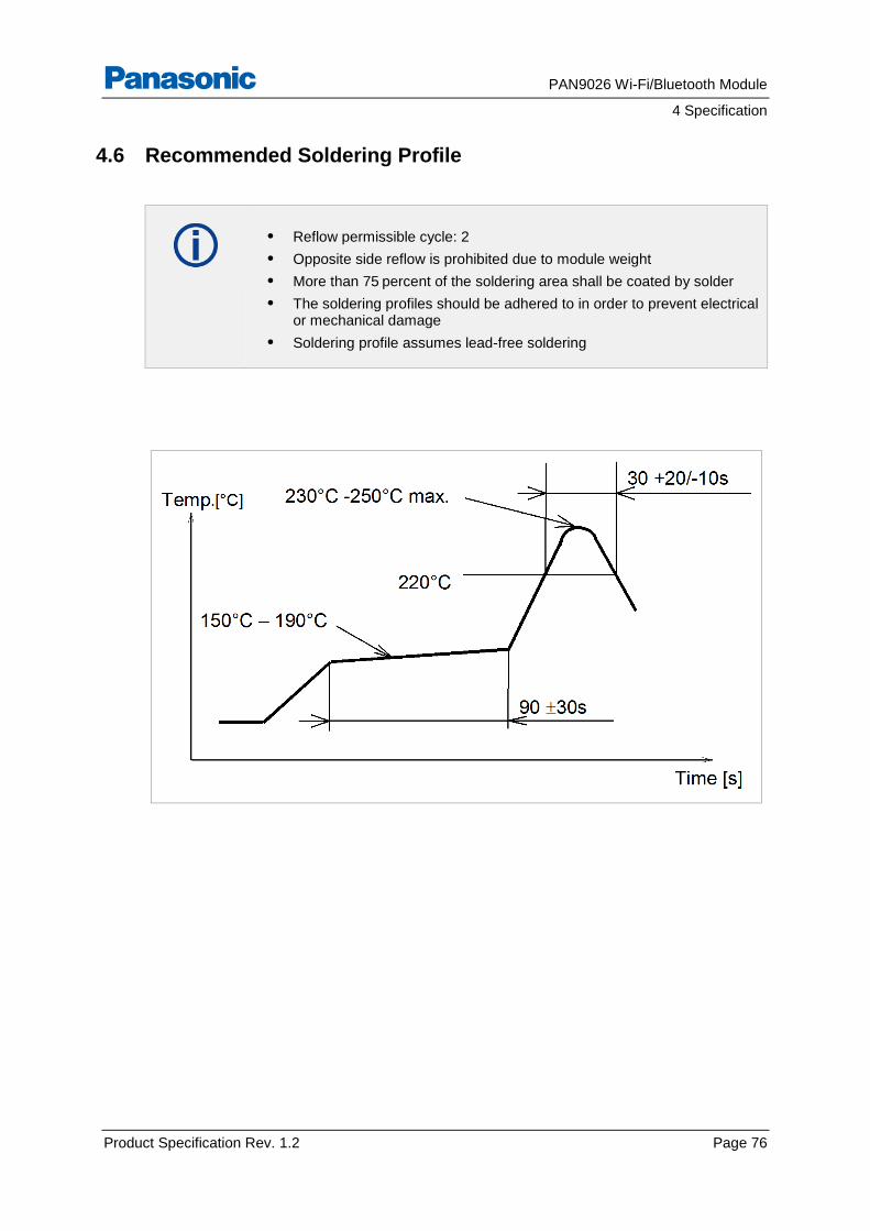
PAN9026 Wi-Fi/Bluetooth Module
4 Specification
Product Specification Rev. 1.2 Page 76
4.6 Recommended Soldering Profile
• Reflow permissible cycle: 2
• Opposite side reflow is prohibited due to module weight
• More than 75 percent of the soldering area shall be coated by solder
• The soldering profiles should be adhered to in order to prevent electrical or mechanical damage
• Soldering profile assumes lead-free soldering
PAN9026 Wi-Fi/Bluetooth Module
5 Cautions
Product Specification Rev. 1.2 Page 77
5 Cautions
Failure to follow the guidelines set forth in this document may result in degrading of the module functions and damage to the module.
5.1 Design Notes
Radio requires a RF ground plane on the rest of the Printed Circuit Board (PCB) area. This can be located on any layer of the PCB. For best performance, extend the RF ground plane the entire length of your board. Connect all ground pins and do not notch the ground plane around the module. The bottom of the module is grounded. So be careful of vias or conductive traces located under the modules that are not soldered masked to prevent shorting.
Keep metallic components, connectors, copper traces, internal layers, and ground planes away from the antenna area in 3D space!
1. Follow the conditions written in this specification, especially the control signals of this
module.
2. The supply voltage should abide by the maximum ratings ( 4.2 Absolute Maximum
Ratings).
3. The supply voltage must be free of AC ripple voltage (for example from a battery or a low
noise regulator output). For noisy supply voltages, provide a decoupling circuit (for
example a ferrite in series connection and a bypass capacitor to ground of at least 47 µF
directly at the module).
4. This module should not be mechanically stressed when installed.
5. Keep this module away from heat. Heat is the major cause of decreasing the life time of
these modules.
6. Avoid assembly and use of the target equipment in conditions where the module
temperature may exceed the maximum tolerance.
7. Keep this module away from other high frequency circuits.
8. Refer to the recommended pattern when designing a board.
5.2 Installation Notes
1. Reflow soldering is possible twice based on the conditions set forth in 4.6
Recommended Soldering Profile. Set up the temperature at the soldering portion of this
module according to this reflow profile.
2. Carefully position the module so that the heat will not burn into printed circuit boards or
affect other components that are susceptible to heat.
3. Carefully locate the module, to avoid an increased temperature caused by heat
generated by neighboring components.
PAN9026 Wi-Fi/Bluetooth Module
5 Cautions
Product Specification Rev. 1.2 Page 78
4. If a vinyl-covered wire comes into contact with the module, the wire cover will melt and
generate toxic gas, damaging the insulation. Never allow contact between a vinyl cover
and these modules to occur.
5. This module should not be mechanically stressed or vibrated when reflowed.
6. To repair the board by hand soldering, follow the conditions set forth in this chapter.
7. Do not wash this product.
8. Pressing on parts of the metal cover or fastening objects to the metal will cause damage
to the module.
5.3 Usage Condition Notes
1. Take measures to protect the module against static electricity.
If pulses or transient loads (a large load, which is suddenly applied) are applied to the
modules, check and evaluate their operation before assembly of the final products.
2. Do not use dropped modules.
3. Do not touch, damage, or soil the pins.
4. Follow the recommended condition ratings about the power supply applied to this
module.
5. Electrode peeling strength: Do not apply a force of more than 4.9 N in any direction on
the soldered module.
6. Pressing on parts of the metal cover or fastening objects to the metal cover will cause
damage.
7. These modules are intended for general purpose and standard use in general electronic
equipment, such as home appliances, office equipment, information, and communication
equipment.
5.4 Storage Notes
1. The module should not be stressed mechanically during storage.
2. Do not store these modules in the following conditions or the performance
characteristics of the module, such as RF performance will be adversely affected:
– Storage in salty air or in an environment with a high concentration of corrosive gas,
such as Cl2, H2S, NH3, SO2, or NOX,
– Storage in direct sunlight,
– Storage in an environment where the temperature may be outside the range of 5 °C to
35 °C, or where the humidity may be outside the 45 % to 85 % range,
– Storage of the modules for more than one year after the date of delivery storage period:
Please check the adhesive strength of the embossed tape and soldering after 6 months
of storage.
3. Keep this module away from water, poisonous gas, and corrosive gas.
4. This module should not be stressed or shocked when transported.
PAN9026 Wi-Fi/Bluetooth Module
5 Cautions
Product Specification Rev. 1.2 Page 79
5. Follow the specification when stacking packed crates (max. 10).
5.5 Safety Cautions
These specifications are intended to preserve the quality assurance of products and individual
components.
Before use, check and evaluate the operation when mounted on your products. Abide by these
specifications without deviation when using the products. These products may short-circuit. If
electrical shocks, smoke, fire, and/or accidents involving human life are anticipated when a
short circuit occurs, provide the following failsafe functions as a minimum:
1. Ensure the safety of the whole system by installing a protection circuit and a protection
device.
2. Ensure the safety of the whole system by installing a redundant circuit or another system
to prevent a single fault causing an unsafe status.
5.6 Other Cautions
1. Do not use the module for other purposes than those listed in section 5.3 Usage
Condition Notes
2. Be sure to provide an appropriate fail-safe function on your product to prevent any
additional damage that may be caused by the abnormal function or the failure of the
module.
3. This module has been manufactured without any ozone chemical controlled under the
Montreal Protocol.
4. These modules are not intended for use under the special conditions shown below.
Before using these modules under such special conditions, carefully check their
performance and reliability under the said special conditions to determine whether or not
they can be used in such a manner:
– In liquid, such as water, salt water, oil, alkali, or organic solvent, or in places where
liquid may splash,
– In direct sunlight, outdoors, or in a dusty environment,
– In an environment where condensation occurs,
– In an environment with a high concentration of harmful gas (e.g. salty air, HCl, Cl2, SO2,
H2S, NH3, and NOX).
5. If an abnormal voltage is applied due to a problem occurring in other components or
circuits, replace these modules with new modules, because they may not be able to
provide normal performance even if their electronic characteristics and appearances
appear satisfactory.
Please refer to the Panasonic website for for further information 7.2.2 Product Information.
PAN9026 Wi-Fi/Bluetooth Module
5 Cautions
Product Specification Rev. 1.2 Page 80
5.7 Restricted Use
5.7.1 Life Support Policy
This Panasonic Industrial Devices Europe GmbH product is not designed for use in life support
appliances, devices, or systems where malfunction can reasonably be expected to result in a
significant personal injury to the user, or as a critical component in any life support device or
system whose failure to perform can be reasonably expected to cause the failure of the life
support device or system, or to affect its safety or effectiveness.
Panasonic customers using or selling these products for use in such applications do so at their
own risk and agree to fully indemnify Panasonic Industrial Devices Europe GmbH for any
damages resulting.
5.7.2 Restricted End Use
This Panasonic Industrial Devices Europe GmbH product is not designed for any restricted
activity that supports the development, production, handling usage, maintenance, storage,
inventory or proliferation of any weapons or military use.
Transfer, export, re-export, usage or reselling of this product to any destination, end-user or any
end-use prohibited by the European Union, United States or any other applicable law is strictly
prohibited.
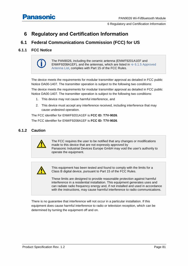
PAN9026 Wi-Fi/Bluetooth Module
6 Regulatory and Certification Information
Product Specification Rev. 1.2 Page 81
6 Regulatory and Certification Information
6.1 Federal Communications Commission (FCC) for US
6.1.1 FCC Notice
The PAN9026, including the ceramic antenna (ENWF9201A1EF and ENWF9208A1EF), and the antennas, which are listed in 6.1.5 Approved Antenna List, complies with Part 15 of the FCC Rules.
The device meets the requirements for modular transmitter approval as detailed in FCC public
Notice DA00-1407. The transmitter operation is subject to the following two conditions:
The device meets the requirements for modular transmitter approval as detailed in FCC public
Notice DA00-1407. The transmitter operation is subject to the following two conditions:
1. This device may not cause harmful interference, and
2. This device must accept any interference received, including interference that may
cause undesired operation.
The FCC identifier for ENWF9201A1EF is FCC ID: T7V-9026.
The FCC identifier for ENWF9208A1EF is FCC ID: T7V-9026.
6.1.2 Caution
The FCC requires the user to be notified that any changes or modifications made to this device that are not expressly approved by Panasonic Industrial Devices Europe GmbH may void the user's authority to operate the equipment.
This equipment has been tested and found to comply with the limits for a Class B digital device, pursuant to Part 15 of the FCC Rules.
These limits are designed to provide reasonable protection against harmful interference in a residential installation. This equipment generates uses and can radiate radio frequency energy and, if not installed and used in accordance with the instructions, may cause harmful interference to radio communications.
There is no guarantee that interference will not occur in a particular installation. If this
equipment does cause harmful interference to radio or television reception, which can be
determined by turning the equipment off and on.
PAN9026 Wi-Fi/Bluetooth Module
6 Regulatory and Certification Information
Product Specification Rev. 1.2 Page 82
It is recommended to try to correct the interference by one or more of the following measures:
• Reorient or relocate the receiving antenna.
• Increase the separation between the equipment and receiver.
• Connect the equipment into an outlet on a circuit different from that to which the receiver is connected.
• Consult the dealer or an experienced radio/TV technician for help.
6.1.3 Label Requirements
The OEM must ensure that FCC labelling requirements are met. This includes a clearly visible label (laser marking) on the outside of the OEM enclosure specifying the appropriate Panasonic FCC identifier for this product as well as the FCC Notice above.
The FCC identifier for model ENWF9201A1EF is FCC ID: T7V-9026.
The FCC identifier for model ENWF9208A1EF is FCC ID: T7V-9026.
This FCC identifier is valid for the PAN9026. The end product must in any case be labelled on
the exterior with:
“Contains FCC ID: T7V-9026”.
6.1.4 Antenna Warning
This antenna warning refers to the test device with the model number ENWF9201A1EF and
ENWF9208A1EF in bottom pad mode RF-Switch Pins Function.
The device is tested with a standard SMA connector and with the antenna listed below. When
integrated into the OEM’s product, these fixed antennas require installation preventing end
users from replacing them with non-approved antennas. Any antenna not in the following table
must be tested to comply with FCC Section 15.203 for unique antenna connectors and with
Section 15.247 for emissions. The FCC identifier for the device with the antenna listed in
6.1.5 Approved Antenna List is the same (FCC ID: T7V-9026).
6.1.5 Approved Antenna List
Item Part Number Manufacturer Type Polarization Frequency Band Gain (dBi)
Min Peak
1 ANT162442DT-
2001A2
TDK Chip
Antenna
Linear 2.400 - 2.484 GHz -36 2.1
5.150 - 5.850 GHz -42 1.5
PAN9026 Wi-Fi/Bluetooth Module
6 Regulatory and Certification Information
Product Specification Rev. 1.2 Page 83
6.1.6 RF Exposure
To comply with FCC RF Exposure requirements, the OEM must ensure that only antennas from the Approved Antenna List are installed 6.1.5 Approved Antenna List.
The preceding statement must be included as a caution statement in manuals for products operating with the approved antennas in the previous table to alert users on FCC RF Exposure compliance.
Any notification to the end user of installation or removal instructions about the integrated radio module is not allowed.
The radiated output power of the PAN9026 with a mounted ceramic chip antenna
(FCC ID: T7V-9026 for model ENWF9201A1EF and ENWF9208A1EF) are
fulfilled for mobile configuration. The installation of the module is restricted to
mobile host devices. The PAN9026 shall be used in such a manner that the
potential for human contact during normal operation is minimized.
End users may not be provided with the module installation instructions. OEM integrators and end users must be provided with transmitter operating conditions for satisfying RF exposure compliance.
6.1.7 Integration Instructions
This chapter gives integration instructions for host product manufacturers according to KDB
996369 D03 OEM Manual v01.
Section Topic and Comment
2.2 List of applicable FCC rules
47 CFR Section Part 15C
Frequency Band (MHz) 2 400 to 2 483.5
Systems Digital Transmission Systems operating within the 2 400 - 2 483.5
MHz Band
Reference / Requirement 15.247(a)(2), 15.247(b)(1), 15.207, 15.247(d), 15.247(e)
Complied Module M/N ENWF9201A1EF, ENWF9208A1EF
47 CFR Section Part 15C
Frequency Band (MHz) 2 400 to 2 483.5
Systems Frequency Hopping Systems operating within the 2 400 - 2 483.5 MHz
Band
Reference / Requirement 15.247(a)(1), 15.247(a)(1)(iii), 15.247(b)(1), 15.207, 15.247(d)
Complied Module M/N ENWF9201A1EF, ENWF9208A1EF
47 CFR Section Part 15E
PAN9026 Wi-Fi/Bluetooth Module
6 Regulatory and Certification Information
Product Specification Rev. 1.2 Page 84
Systems Unlicensed National Information Infrastructure Devices in the 5 GHz
Bands
Reference Method KDB 905462 D02 v02
Reference / Requirement 15E.407(h)(2)
Complied Module M/N ENWF9201A1EF
2.3 Summarize the specific operational use conditions
Please refer to sections 5 Cautions, 5.3 Usage Condition Notes, and 6.1.5 Approved Antenna
List.
2.4 Limited module procedures
Not applicable, the module has a single-modular transmitter approval.
2.5 Trace antenna designs
Not applicable, the module has a ceramic chip antenna. For guidance regarding the PCB layout
requirements for module integration refer to the Design Guide 7.2.2 Product Information.
2.6 RF exposure considerations
Mobile application, the end customer has to assure that the device has a distance of more than
20 cm from the human body under all circumstances.
2.7 Antennas
Please refer to sections 6.1.4 Antenna Warning and 6.1.5 Approved Antenna List.
2.8 Label and compliance information
Please refer to section 6.1.3 Label Requirements.
2.9 Information on test modes and additional testing requirements
The documents for integration guidance and compliance testing are available here 7.2.2
Product Information.
2.10 Additional testing, Part 15 Subpart B disclaimer
The single-modular transmitter is FCC authorized for the specific rule parts listed at section List
of applicable FCC rules.
The host product manufacturer needs to also consider the FCC requirements for certified modular
transmitter being used in the host product and maintain documentation on how the host product
with the certified modular transmitter complies with the FCC rules. Host product manufacturers are
responsible to follow the integration guidance and to perform a limited set of transmitter module
verification testing, to ensure the end product is in compliance with the FCC rules. Also host
product manufacturers are responsible for all additional equipment authorization and testing for
technical requirements not covered by the module grant (e.g., unintentional radiator Part 15
Subpart B requirements, or transmitters used in the host that are not certified modules).
PAN9026 Wi-Fi/Bluetooth Module
6 Regulatory and Certification Information
Product Specification Rev. 1.2 Page 85
6.2 Innovation, Science, and Economic Development (ISED) for
Canada
English
PAN9026 and versions are licensed to meet the regulatory requirements of ISED.
License for M/N: ENWF9203A1EF: IC: 216Q-9026
License for M/N: ENWF9208A1EF: IC: 216Q-9026
Manufacturers of mobile, fixed, or portable devices incorporating this module are advised to
clarify any regulatory questions and ensure compliance for SAR and/or RF exposure limits.
Users can obtain Canadian information on RF exposure and compliance from www.ic.gc.ca.
This device has been designed to operate with the antennas listed in 6.1.5 Approved
Antenna List, having a maximum gain of 2.1 dBi for 2.4 GHz and 1.5 dBi for 5 GHz. Antennas
not included in this list or having a gain greater than 2.1 dBi for 2.4 GHz and 1.5 dBi for 5 GHz
are strictly prohibited for use with this device. The required antenna impedance is 50 Ω. The
antenna used for this transmitter must not be co-located or operating in conjunction with any
other antenna or transmitter.
French
PAN9026 (et ses versions) est garanti conforme aux dispositions règlementaires d’Innovation,
Sciences et Développement économique (ISDE).
Licence pour M/N: ENWF9203A1EF: IC: 216Q-9026
Licence pour M/N: ENWF9208A1EF: IC: 216Q-9026
Il est recommandé aux fabricants d’appareils fixes, mobiles ou portables de consulter la
réglementation en vigueur et de vérifier la conformité de leurs produits relativement aux limites
d’exposition aux rayonnements radiofréquence ainsi qu’au débit d’absorption spécifique
maximum autorisé.
Des informations pour les utilisateurs sur la réglementation Canadienne concernant l’exposition
aux rayonnements RF sont disponibles sur le site www.ic.gc.ca.
Ce produit a été développé pour fonctionner spécifiquement avec les antennes listées dans le
tableau 6.1.5 Approved Antenna List, présentant un gain maximum de 2.1 dBi pour 2.4 GHz
et 1.5 dBi pour 5 GHz. Des antennes autres que celles listées ici, ou présentant un gain
supérieur à 2.1 dBi pour 2.4 GHz et 1.5 dBi pour 5 GHz ne doivent en aucune circonstance être
utilises en combinaison avec ce produit. L’impédance des antennes compatibles est 50 Ω.
L’antenne utilisée avec ce produit ne doit ni être située à proximité d’une autre antenne ou d’un
autre émetteur, ni être utilisée conjointement avec une autre antenne ou un autre émetteur.
PAN9026 Wi-Fi/Bluetooth Module
6 Regulatory and Certification Information
Product Specification Rev. 1.2 Page 86
6.2.1 Radio Standards Specification RSS-247 Issue 2
The Radio Standards Specification RSS-247, Issue 2, Digital Transmission Systems (DTSs),
Frequency Hopping Systems (FHSs) and License-Exempt Local Area Network (LE-LAN)
Devices, replaces RSS-247, Issue 1, dated May 2015. It sets out certification requirements for
radio apparatus operating in the bands 2 400 MHz to 2 483.5 MHz and 5 725 MHz to 5 850 MHz
employing frequency hopping, digital modulation and/or a combination (hybrid) of both
techniques. It also includes license exempt local area network (LE-LAN) devices operating in
the bands 5 150 MHz to 5 250 MHz, 5 250 MHz to 5 350 MHz, 5 470 MHz to 5 725 MHz and
5 725 MHz to 5 850 MHz as specified in SP-5 150 MHz.
6.2.1.1 General
Equipment covered by the standard RSS-247 is classified as Category I equipment. Either a
technical acceptance certificate (TAC) issued by the Certification and Engineering Bureau of
Innovation, Science and Economic Development Canada (ISED) or a certificate issued by a
certification body (CB) is required.
6.2.1.2 Certification Requirements
RSS-247 shall be used in conjunction with RSS-Gen, General Requirements for Compliance of
Radio Apparatus, for general specifications and information relevant to the equipment for which
this standard applies. Equipment certified under the standard is required to comply with the
provisions in RSS‑Gen with respect to emissions falling within restricted frequency bands.
These restricted frequency bands are listed in RSS‑Gen.
6.2.1.3 Measurement Method
In addition to the requirements in RSS-Gen and the requirements of the standard RSS-247, the
method for measuring DTS devices is provided in ANSI C63.10.
6.2.1.4 FHS and DTS operating in the bands 2 400 MHz to 2 483.5 MHz
This section applies to frequency hopping systems (FHSs) in the bands 2 400 MHz to
2 483.5 MHz and 5 725 MHz to 5 850 MHz and digital transmission systems (DTSs) in the band
2 400 MHz to 2 483.5 MHz. Systems in these bands can be frequency hopping, digital
transmission and/or a combination (hybrid) of both types. The digital transmission technology of
DTSs or hybrid systems operating in the band 5 725 MHz to 5 850 MHz shall comply with the
requirement in section Technical requirements for license-exempt local area network devices
and digital transmission systems operating in the 5 GHz band.
PAN9026 Wi-Fi/Bluetooth Module
6 Regulatory and Certification Information
Product Specification Rev. 1.2 Page 87
RSS-247 Section 5.1
Frequency Band (MHz) 2 400 to 2 483.5
Systems Frequency Hopping Systems
Systems out of Scope FHS operating in the band 5 725 MHz to 5 850 MHz
Fixed point-to-point systems
Requirements The maximum peak conducted output power shall not exceed W if the hopset
uses 75 or more hopping channels; the maximum peak conducted output
power shall not exceed 0.125 W if the hopset uses less than 75 hopping
channels.
Complied Module M/N ENWF9203A1EF, ENWF9208A1EF
RSS-247 Section 5.2
Frequency Band (MHz) 2 400 to 2 483.5
Systems Digital Transmission Systems
Systems out of Scope -
Requirements The minimum 6 dB bandwidth shall be 500 kHz.
The transmitter power spectral density conducted from the transmitter to the
antenna shall not be greater than 8 dBm in any 3 kHz band during any time
interval of continuous transmission.
The maximum peak conducted output power shall not exceed 1 W. The e.i.r.p.
shall not exceed 4 W.
Complied Module M/N ENWF9203A1EF, ENWF9208A1EF
RSS-247 Section 5.3
Frequency Band (MHz) 2 400 to 2 483.5
Systems Hybrid Systems
Systems out of Scope Hybrid devices operating in the band 5 725 MHz to 5 850 MHz.
Requirements With the digital transmission operation of the hybrid system turned off, the
frequency hopping operation shall have an average time of occupancy on any
frequency not exceeding 0.4 seconds within a duration in seconds equal to the
number of hopping frequencies multiplied by 0.4.
With the frequency hopping turned off, the digital transmission operation shall
comply with the power spectral density requirements for digital modulation
systems set out in section “5.2” RSS-247 Section.
Complied Module M/N ENWF9203A1EF, ENWF9208A1EF
PAN9026 Wi-Fi/Bluetooth Module
6 Regulatory and Certification Information
Product Specification Rev. 1.2 Page 88
RSS-247 Section 5.4
Frequency Band (MHz) 2 400 to 2 483.5
Systems FHSs operating in the band 2 400 to 2 483.5 MHz.
DTSs employing digital modulation techniques operating in the band
2 400 MHz to 2 483.5 MHz.
Systems out of Scope FHSs operating in the band 902 MHz to 928 MHz and 5 725 MHz to
5 850 MHz.
DTSs employing digital modulation techniques operating in the bands
902 MHz to 928 MHz.
Fixed point-to-point systems in the bands 2 400 MHz to 2 483.5 MHz and
5 725 MHz to 5 850 MHz.
Transmitters operating in the band 2 400 MHz to 2 483.5 MHz, may employ
antenna systems that emit multiple directional beams simultaneously or
sequentially.
Requirements Transmitter Output Power:
The maximum peak conducted output power shall not exceed 1 W if the
hopset uses 75 or more hopping channels; the maximum peak conducted
output power shall not exceed 0.125 W if the hopset uses less than 75
hopping channels. The e.i.r.p. shall not exceed 4 W.
For DTSs employing digital modulation techniques operating in the band
2 400 MHz to 2 483.5 MHz, the maximum peak conducted output power shall
not exceed W. The e.i.r.p. shall not exceed 4 W.
Complied Module M/N ENWF9203A1EF, ENWF9208A1EF
RSS-247 Section 5.5
Frequency Band (MHz) 2 400 to 2 483.5
System In any 100 kHz bandwidth outside the frequency band in which the spread
spectrum or digitally modulated device is operating …
System out of Scope -
Requirements Unwanted Emissions:
In any 100 kHz bandwidth outside the frequency band in which the spread
spectrum or digitally modulated device is operating, the RF power that is
produced shall be at least 20 dB below that in the 100 kHz bandwidth within
the band that contains the highest level of the desired power, based on either
an RF conducted or a radiated measurement, provided that the transmitter
demonstrates compliance with the peak conducted power limits. If the
transmitter complies with the conducted power limits based on the use of root-
mean-square averaging over a time interval the attenuation required shall be
30 dB instead of 20 dB. Attenuation below the general field strength limits
specified in RSS-Gen is not required.
Complied Module M/N ENWF9203A1EF, ENWF9208A1EF
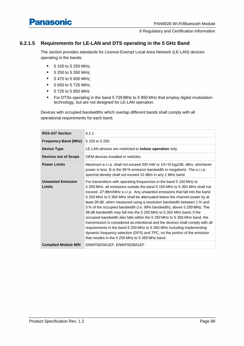
PAN9026 Wi-Fi/Bluetooth Module
6 Regulatory and Certification Information
Product Specification Rev. 1.2 Page 89
6.2.1.5 Requirements for LE-LAN and DTS operating in the 5 GHz Band
The section provides standards for Licence-Exempt Local Area Network (LE-LAN) devices
operating in the bands:
• 5 150 to 5 250 MHz,
• 5 250 to 5 350 MHz,
• 5 470 to 5 600 MHz,
• 5 650 to 5 725 MHz,
• 5 725 to 5 850 MHz
• For DTSs operating in the band 5 725 MHz to 5 850 MHz that employ digital modulation technology, but are not designed for LE-LAN operation.
Devices with occupied bandwidths which overlap different bands shall comply with all
operational requirements for each band.
RSS-247 Section 6.2.1
Frequency Band (MHz) 5 150 to 5 250
Device Type LE-LAN devices are restricted to indoor operation only.
Devices out of Scope OEM devices installed in vehicles.
Power Limits Maximum e.i.r.p. shall not exceed 200 mW or 10+10 log10B, dBm, whichever
power is less. B is the 99 % emission bandwidth in megahertz. The e.i.r.p.
spectral density shall not exceed 10 dBm in any 1 MHz band.
Unwanted Emission
Limits
For transmitters with operating frequencies in the band 5 150 MHz to
5 250 MHz, all emissions outside the band 5 150 MHz to 5 350 MHz shall not
exceed -27 dBm/MHz e.i.r.p. Any unwanted emissions that fall into the band
5 250 MHz to 5 350 MHz shall be attenuated below the channel power by at
least 26 dB, when measured using a resolution bandwidth between 1 % and
5 % of the occupied bandwidth (i.e. 99% bandwidth), above 5 250 MHz. The
26 dB bandwidth may fall into the 5 250 MHz to 5 350 MHz band; if the
occupied bandwidth also falls within the 5 250 MHz to 5 350 MHz band, the
transmission is considered as intentional and the devices shall comply with all
requirements in the band 5 250 MHz to 5 350 MHz including implementing
dynamic frequency selection (DFS) and TPC, on the portion of the emission
that resides in the 5 250 MHz to 5 350 MHz band.
Complied Module M/N ENWF9203A1EF, ENWF9208A1EF
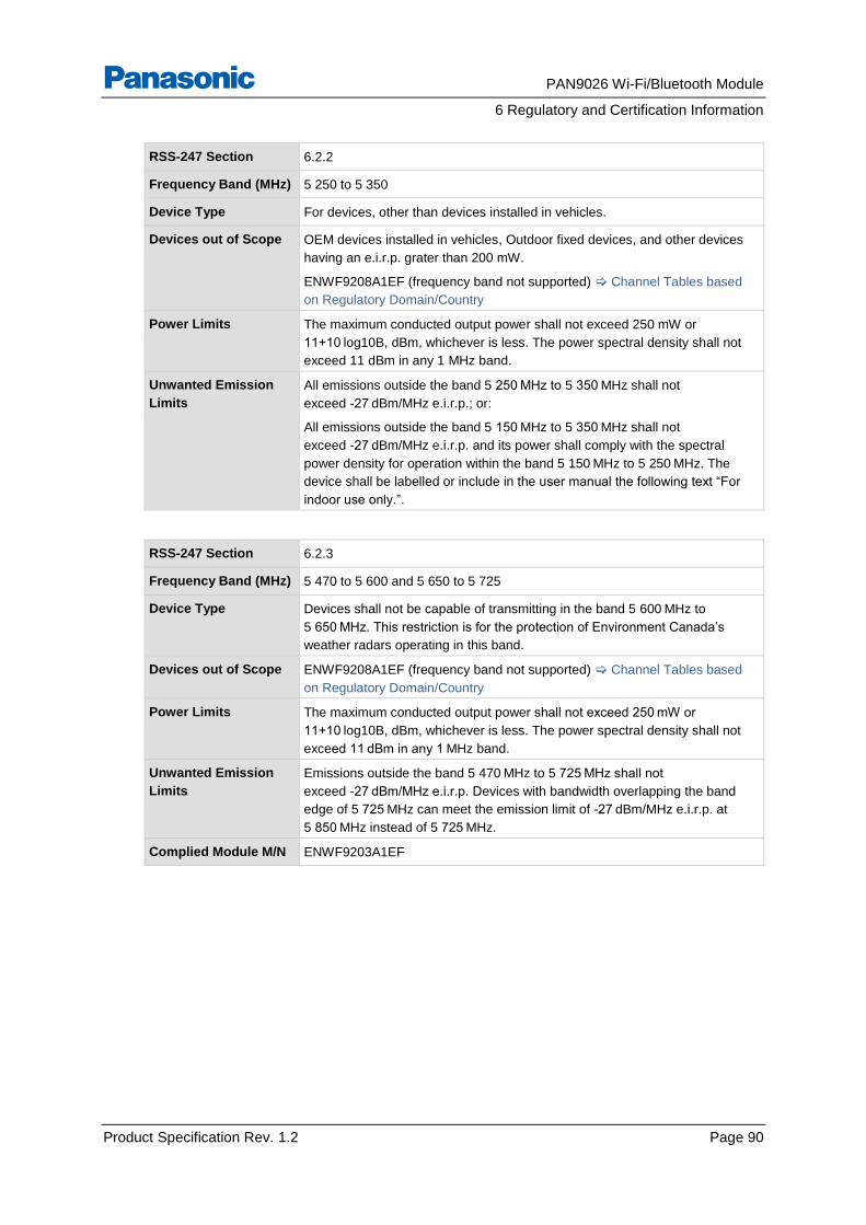
PAN9026 Wi-Fi/Bluetooth Module
6 Regulatory and Certification Information
Product Specification Rev. 1.2 Page 90
RSS-247 Section 6.2.2
Frequency Band (MHz) 5 250 to 5 350
Device Type For devices, other than devices installed in vehicles.
Devices out of Scope OEM devices installed in vehicles, Outdoor fixed devices, and other devices
having an e.i.r.p. grater than 200 mW.
ENWF9208A1EF (frequency band not supported) Channel Tables based
on Regulatory Domain/Country
Power Limits The maximum conducted output power shall not exceed 250 mW or
11+10 log10B, dBm, whichever is less. The power spectral density shall not
exceed 11 dBm in any 1 MHz band.
Unwanted Emission
Limits
All emissions outside the band 5 250 MHz to 5 350 MHz shall not
exceed -27 dBm/MHz e.i.r.p.; or:
All emissions outside the band 5 150 MHz to 5 350 MHz shall not
exceed -27 dBm/MHz e.i.r.p. and its power shall comply with the spectral
power density for operation within the band 5 150 MHz to 5 250 MHz. The
device shall be labelled or include in the user manual the following text “For
indoor use only.”.
RSS-247 Section 6.2.3
Frequency Band (MHz) 5 470 to 5 600 and 5 650 to 5 725
Device Type Devices shall not be capable of transmitting in the band 5 600 MHz to
5 650 MHz. This restriction is for the protection of Environment Canada’s
weather radars operating in this band.
Devices out of Scope ENWF9208A1EF (frequency band not supported) Channel Tables based
on Regulatory Domain/Country
Power Limits The maximum conducted output power shall not exceed 250 mW or
11+10 log10B, dBm, whichever is less. The power spectral density shall not
exceed 11 dBm in any 1 MHz band.
Unwanted Emission
Limits
Emissions outside the band 5 470 MHz to 5 725 MHz shall not
exceed -27 dBm/MHz e.i.r.p. Devices with bandwidth overlapping the band
edge of 5 725 MHz can meet the emission limit of -27 dBm/MHz e.i.r.p. at
5 850 MHz instead of 5 725 MHz.
Complied Module M/N ENWF9203A1EF
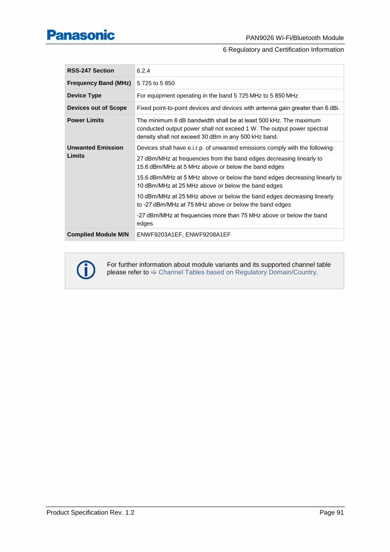
PAN9026 Wi-Fi/Bluetooth Module
6 Regulatory and Certification Information
Product Specification Rev. 1.2 Page 91
RSS-247 Section 6.2.4
Frequency Band (MHz) 5 725 to 5 850
Device Type For equipment operating in the band 5 725 MHz to 5 850 MHz
Devices out of Scope Fixed point-to-point devices and devices with antenna gain greater than 6 dBi.
Power Limits The minimum 6 dB bandwidth shall be at least 500 kHz. The maximum
conducted output power shall not exceed 1 W. The output power spectral
density shall not exceed 30 dBm in any 500 kHz band.
Unwanted Emission
Limits
Devices shall have e.i.r.p. of unwanted emissions comply with the following:
27 dBm/MHz at frequencies from the band edges decreasing linearly to
15.6 dBm/MHz at 5 MHz above or below the band edges
15.6 dBm/MHz at 5 MHz above or below the band edges decreasing linearly to
10 dBm/MHz at 25 MHz above or below the band edges
10 dBm/MHz at 25 MHz above or below the band edges decreasing linearly
to -27 dBm/MHz at 75 MHz above or below the band edges
-27 dBm/MHz at frequencies more than 75 MHz above or below the band
edges
Complied Module M/N ENWF9203A1EF, ENWF9208A1EF
For further information about module variants and its supported channel table please refer to Channel Tables based on Regulatory Domain/Country.
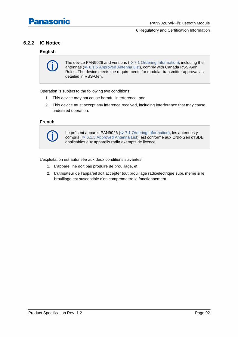
PAN9026 Wi-Fi/Bluetooth Module
6 Regulatory and Certification Information
Product Specification Rev. 1.2 Page 92
6.2.2 IC Notice
English
The device PAN9026 and versions ( 7.1 Ordering Information), including the antennas ( 6.1.5 Approved Antenna List), comply with Canada RSS-Gen Rules. The device meets the requirements for modular transmitter approval as detailed in RSS-Gen.
Operation is subject to the following two conditions:
1. This device may not cause harmful interference, and
2. This device must accept any inference received, including interference that may cause
undesired operation.
French
Le présent appareil PAN9026 ( 7.1 Ordering Information), les antennes y compris ( 6.1.5 Approved Antenna List), est conforme aux CNR-Gen d'ISDE applicables aux appareils radio exempts de licence.
L'exploitation est autorisée aux deux conditions suivantes:
1. L'appareil ne doit pas produire de brouillage, et
2. L'utilisateur de l'appareil doit accepter tout brouillage radioélectrique subi, même si le
brouillage est susceptible d'en compromettre le fonctionnement.
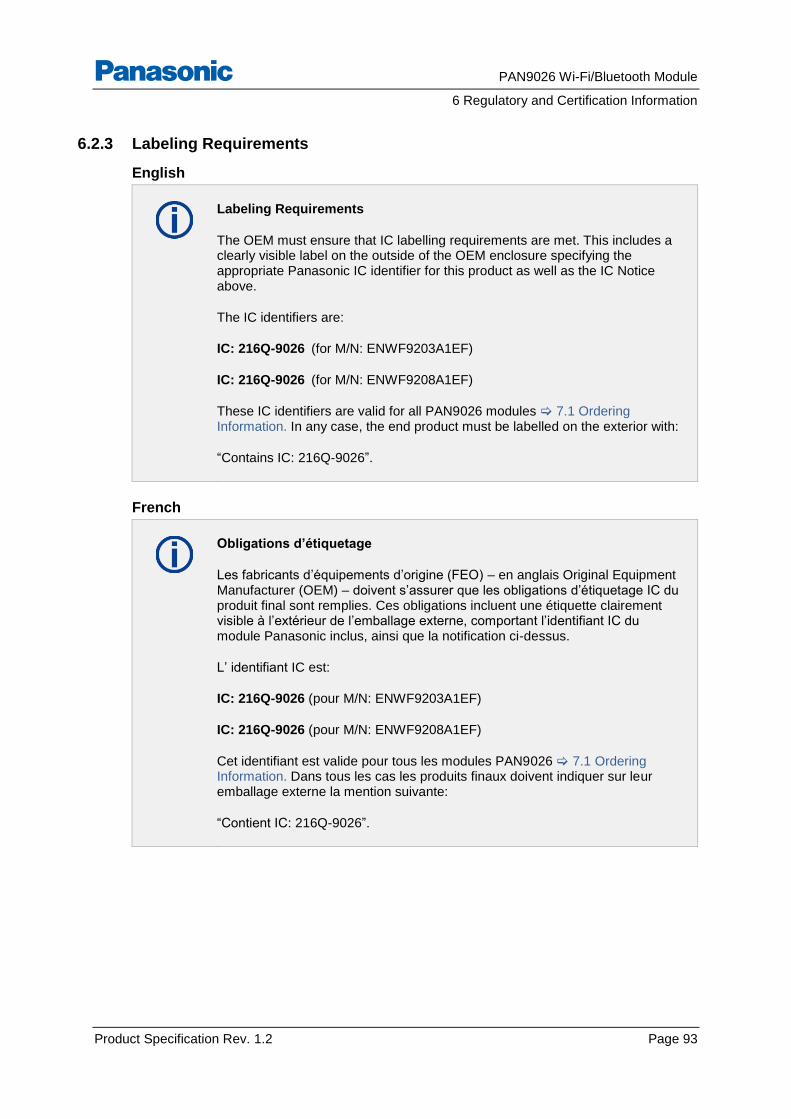
PAN9026 Wi-Fi/Bluetooth Module
6 Regulatory and Certification Information
Product Specification Rev. 1.2 Page 93
6.2.3 Labeling Requirements
English
Labeling Requirements
The OEM must ensure that IC labelling requirements are met. This includes a clearly visible label on the outside of the OEM enclosure specifying the appropriate Panasonic IC identifier for this product as well as the IC Notice above.
The IC identifiers are:
IC: 216Q-9026 (for M/N: ENWF9203A1EF)
IC: 216Q-9026 (for M/N: ENWF9208A1EF)
These IC identifiers are valid for all PAN9026 modules 7.1 Ordering Information. In any case, the end product must be labelled on the exterior with:
“Contains IC: 216Q-9026”.
French
Obligations d’étiquetage
Les fabricants d’équipements d’origine (FEO) – en anglais Original Equipment Manufacturer (OEM) – doivent s’assurer que les obligations d’étiquetage IC du produit final sont remplies. Ces obligations incluent une étiquette clairement visible à l’extérieur de l’emballage externe, comportant l’identifiant IC du module Panasonic inclus, ainsi que la notification ci-dessus.
L’ identifiant IC est:
IC: 216Q-9026 (pour M/N: ENWF9203A1EF)
IC: 216Q-9026 (pour M/N: ENWF9208A1EF)
Cet identifiant est valide pour tous les modules PAN9026 7.1 Ordering Information. Dans tous les cas les produits finaux doivent indiquer sur leur emballage externe la mention suivante:
“Contient IC: 216Q-9026”.
PAN9026 Wi-Fi/Bluetooth Module
6 Regulatory and Certification Information
Product Specification Rev. 1.2 Page 94
6.3 European Conformity According to RED (2014/53/EU)
The PAN9026 modules with model number ENWF9202A1EF and ENWF9208A1EF comply with
the standards according to the following LVD (2014/35/EU), EMC-D (2014/30/EU) together with
RED (2014/53/EU) articles:
3.1a Safety/Health: EN 62368-1:2014
EN 62311:2008
3.1b EMC: EN 301 489-1 V2.1.1:2017-02
EN 301 489-17 V3.1.1:2017-02
3.2 Radio: EN 300 328 V2.1.1:2016-11
EN 301 893 V2.1.1:2017-04
EN 300 440 V2.1.1:2017-03
As a result of the conformity assessment procedure described in 2014/53/EU Directive, the
end customer equipment should be labelled as follows:
The end customer has to assure that the device has a distance of more than 20 cm from the human body under all circumstances.
The end customer equipment must meet the actual Safety/Health requirements according to RED.
PAN9026 and its model versions in the specified reference design can be used in all countries
of the European Economic Area (Member States of the EU, European Free Trade Association
States [Iceland, Liechtenstein, and Norway]), Monaco, San Marino, Andorra, and Turkey.
6.3.1 Radio Equipment Directive
The Radio Equipment Directive 2014/53/EU (RED) establishes a regulatory framework for
placing radio equipment on the market. It ensures a Single Market for radio equipment by
setting essential requirements for safety and health, electromagnetic compatibility, and the
efficient use of the radio spectrum.
The RED aligned the previous Directive, the Radio and Telecommunication Terminal Equipment
Directive 1999/5/EC (R&TTED), with the new legislative framework for the marketing of
products. The RED is applicable as of 2016-06-13. It included a one-year transitional period,
which ended on 2017-06-12 (Article 48). On 2017-06-20, the Commission Implementing
PAN9026 Wi-Fi/Bluetooth Module
6 Regulatory and Certification Information
Product Specification Rev. 1.2 Page 95
Regulation (EU) 2017/1354 was adopted. This specifies how to present the information
provided for in Article 10(10) of Directive 2014/53/EU.
Article 10(10) RED
In cases of restrictions on putting into service or of requirements for authorisation of use,
information available on the packaging shall allow the identification of the Member States or the
geographical area within a Member State where restrictions on putting into service or
requirements for authorisation of use exist. Such information shall be completed in the
instructions accompanying the radio equipment. The Commission may adopt implementing acts
specifying how to present that information. Those implementing acts shall be adopted in
accordance with the advisory procedure referred to in Article 45(2).
• Class 1: Radio equipment that can be operated without any restriction in EU, EEA, and EFTA. According to Article 8(1)b of the RED, it is clarified that no national radio interfaces specifications are required to be notified under RED;
• Class 2: Radio equipment subject to restrictions in one or more EU, EEA and EFTA countries where:
– The technical parameters are not harmonised through EU, EEA, and EFTA;
– The technical parameters are harmonised through EU, EEA and EFTA, and do not
fall in above class 1 definition.
Radio equipment class means a class identifying particular categories of radio equipment
which, under this Directive, are considered similar and those radio interfaces for which the radio
equipment is designed.
Article 8 RED
Notification of radio interface specifications and assignment of radio equipment classes 1:
1) Member States shall notify, in accordance with the procedure set out in Directive 98/34/EC,
the radio interfaces which they intend to regulate except:
a) The radio interfaces which fully and without any deviation comply with the Commission
decisions on the harmonised use of radio spectrum adopted pursuant to Decision
No. 676/2002/EC; and
b) The radio interfaces which, in accordance with implementing acts adopted pursuant to
paragraph 2 of this Article, correspond to radio equipment which can be put into service
and used without restrictions within the Union.
2) The Commission shall adopt implementing acts establishing the equivalence between
notified radio interfaces and assigning a radio equipment class, details of which shall be
published in the Official Journal of the European Union. Those implementing acts shall be
adopted in accordance with the examination procedure referred to in Article 45(3).
The Radio Interface Specifications Templates are provided for information in the EFIS database
for applications which use is in harmonised radio spectrum, however with restrictions.
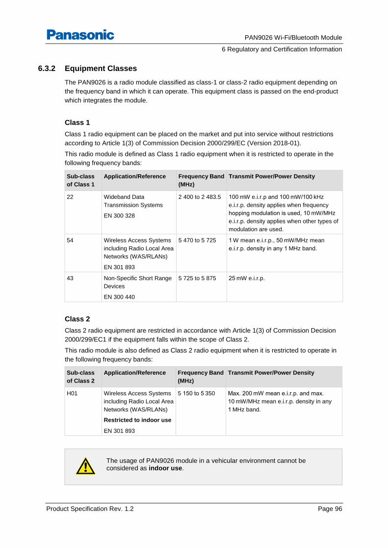
PAN9026 Wi-Fi/Bluetooth Module
6 Regulatory and Certification Information
Product Specification Rev. 1.2 Page 96
6.3.2 Equipment Classes
The PAN9026 is a radio module classified as class-1 or class-2 radio equipment depending on
the frequency band in which it can operate. This equipment class is passed on the end-product
which integrates the module.
Class 1
Class 1 radio equipment can be placed on the market and put into service without restrictions
according to Article 1(3) of Commission Decision 2000/299/EC (Version 2018-01).
This radio module is defined as Class 1 radio equipment when it is restricted to operate in the
following frequency bands:
Sub-class
of Class 1
Application/Reference Frequency Band
(MHz)
Transmit Power/Power Density
22 Wideband Data
Transmission Systems
EN 300 328
2 400 to 2 483.5 100 mW e.i.r.p and 100 mW/100 kHz
e.i.r.p. density applies when frequency
hopping modulation is used, 10 mW/MHz
e.i.r.p. density applies when other types of
modulation are used.
54 Wireless Access Systems
including Radio Local Area
Networks (WAS/RLANs)
EN 301 893
5 470 to 5 725 1 W mean e.i.r.p., 50 mW/MHz mean
e.i.r.p. density in any 1 MHz band.
43 Non-Specific Short Range
Devices
EN 300 440
5 725 to 5 875 25 mW e.i.r.p.
Class 2
Class 2 radio equipment are restricted in accordance with Article 1(3) of Commission Decision
2000/299/EC1 if the equipment falls within the scope of Class 2.
This radio module is also defined as Class 2 radio equipment when it is restricted to operate in
the following frequency bands:
Sub-class
of Class 2
Application/Reference Frequency Band
(MHz)
Transmit Power/Power Density
H01 Wireless Access Systems
including Radio Local Area
Networks (WAS/RLANs)
Restricted to indoor use
EN 301 893
5 150 to 5 350 Max. 200 mW mean e.i.r.p. and max.
10 mW/MHz mean e.i.r.p. density in any
1 MHz band.
The usage of PAN9026 module in a vehicular environment cannot be considered as indoor use.
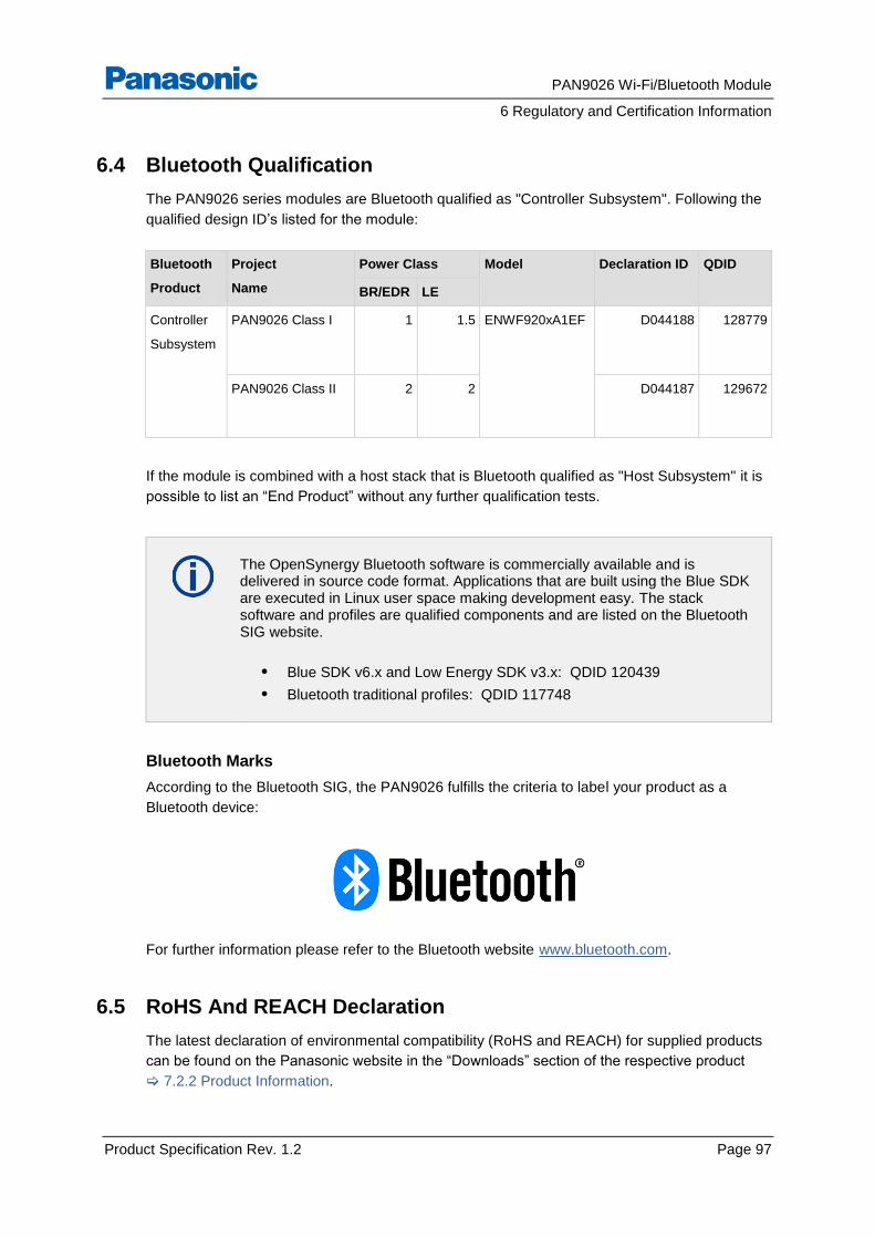
PAN9026 Wi-Fi/Bluetooth Module
6 Regulatory and Certification Information
Product Specification Rev. 1.2 Page 97
6.4 Bluetooth Qualification
The PAN9026 series modules are Bluetooth qualified as "Controller Subsystem". Following the
qualified design ID’s listed for the module:
If the module is combined with a host stack that is Bluetooth qualified as "Host Subsystem" it is
possible to list an “End Product” without any further qualification tests.
The OpenSynergy Bluetooth software is commercially available and is delivered in source code format. Applications that are built using the Blue SDK are executed in Linux user space making development easy. The stack software and profiles are qualified components and are listed on the Bluetooth SIG website.
• Blue SDK v6.x and Low Energy SDK v3.x: QDID 120439
• Bluetooth traditional profiles: QDID 117748
Bluetooth Marks
According to the Bluetooth SIG, the PAN9026 fulfills the criteria to label your product as a
Bluetooth device:
For further information please refer to the Bluetooth website www.bluetooth.com.
6.5 RoHS And REACH Declaration
The latest declaration of environmental compatibility (RoHS and REACH) for supplied products
can be found on the Panasonic website in the “Downloads” section of the respective product
7.2.2 Product Information.
Bluetooth
Product
Project
Name
Power Class Model Declaration ID QDID
BR/EDR LE
Controller
Subsystem
PAN9026 Class I 1 1.5 ENWF920xA1EF D044188 128779
PAN9026 Class II 2 2 D044187 129672
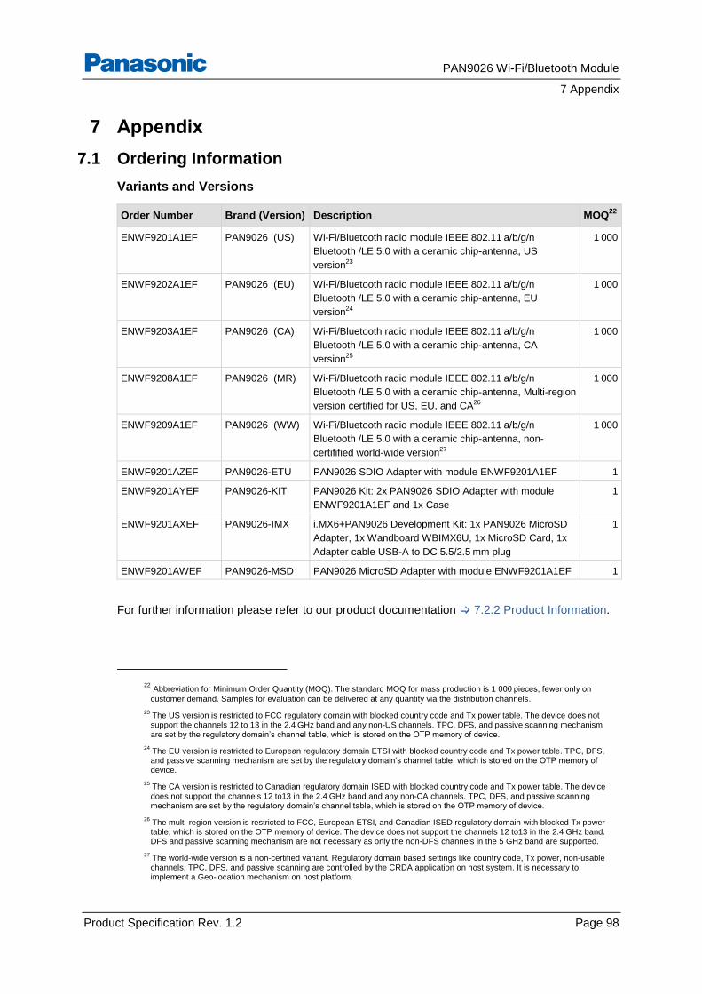
PAN9026 Wi-Fi/Bluetooth Module
7 Appendix
Product Specification Rev. 1.2 Page 98
7 Appendix
7.1 Ordering Information
Variants and Versions
Order Number Brand (Version) Description MOQ22
ENWF9201A1EF PAN9026 (US) Wi-Fi/Bluetooth radio module IEEE 802.11 a/b/g/n
Bluetooth /LE 5.0 with a ceramic chip-antenna, US
version23
1 000
ENWF9202A1EF PAN9026 (EU) Wi-Fi/Bluetooth radio module IEEE 802.11 a/b/g/n
Bluetooth /LE 5.0 with a ceramic chip-antenna, EU
version24
1 000
ENWF9203A1EF PAN9026 (CA) Wi-Fi/Bluetooth radio module IEEE 802.11 a/b/g/n
Bluetooth /LE 5.0 with a ceramic chip-antenna, CA
version25
1 000
ENWF9208A1EF PAN9026 (MR) Wi-Fi/Bluetooth radio module IEEE 802.11 a/b/g/n
Bluetooth /LE 5.0 with a ceramic chip-antenna, Multi-region
version certified for US, EU, and CA26
1 000
ENWF9209A1EF PAN9026 (WW) Wi-Fi/Bluetooth radio module IEEE 802.11 a/b/g/n
Bluetooth /LE 5.0 with a ceramic chip-antenna, non-
certifified world-wide version27
1 000
ENWF9201AZEF PAN9026-ETU PAN9026 SDIO Adapter with module ENWF9201A1EF 1
ENWF9201AYEF PAN9026-KIT PAN9026 Kit: 2x PAN9026 SDIO Adapter with module
ENWF9201A1EF and 1x Case
1
ENWF9201AXEF PAN9026-IMX i.MX6+PAN9026 Development Kit: 1x PAN9026 MicroSD
Adapter, 1x Wandboard WBIMX6U, 1x MicroSD Card, 1x
Adapter cable USB-A to DC 5.5/2.5 mm plug
1
ENWF9201AWEF PAN9026-MSD PAN9026 MicroSD Adapter with module ENWF9201A1EF 1
For further information please refer to our product documentation 7.2.2 Product Information.
22
Abbreviation for Minimum Order Quantity (MOQ). The standard MOQ for mass production is 1 000 pieces, fewer only on
customer demand. Samples for evaluation can be delivered at any quantity via the distribution channels.
23 The US version is restricted to FCC regulatory domain with blocked country code and Tx power table. The device does not support the channels 12 to 13 in the 2.4 GHz band and any non-US channels. TPC, DFS, and passive scanning mechanism are set by the regulatory domain’s channel table, which is stored on the OTP memory of device.
24 The EU version is restricted to European regulatory domain ETSI with blocked country code and Tx power table. TPC, DFS, and passive scanning mechanism are set by the regulatory domain’s channel table, which is stored on the OTP memory of device.
25 The CA version is restricted to Canadian regulatory domain ISED with blocked country code and Tx power table. The device does not support the channels 12 to13 in the 2.4 GHz band and any non-CA channels. TPC, DFS, and passive scanning mechanism are set by the regulatory domain’s channel table, which is stored on the OTP memory of device.
26 The multi-region version is restricted to FCC, European ETSI, and Canadian ISED regulatory domain with blocked Tx power table, which is stored on the OTP memory of device. The device does not support the channels 12 to13 in the 2.4 GHz band. DFS and passive scanning mechanism are not necessary as only the non-DFS channels in the 5 GHz band are supported.
27 The world-wide version is a non-certified variant. Regulatory domain based settings like country code, Tx power, non-usable channels, TPC, DFS, and passive scanning are controlled by the CRDA application on host system. It is necessary to implement a Geo-location mechanism on host platform.
PAN9026 Wi-Fi/Bluetooth Module
7 Appendix
Product Specification Rev. 1.2 Page 99
7.2 Contact Details
7.2.1 Contact Us
Please contact your local Panasonic Sales office for details on additional product options and
services:
For Panasonic Sales assistance in the EU, visit
https://eu.industrial.panasonic.com/about-us/contact-us
Email: [email protected]
For Panasonic Sales assistance in North America, visit the Panasonic Sales & Support Tool to
find assistance near you at
https://na.industrial.panasonic.com/distributors
Please visit the Panasonic Wireless Technical Forum to submit a question at
https://forum.na.industrial.panasonic.com
7.2.2 Product Information
Please refer to the Panasonic Wireless Connectivity website for further information on our
products and related documents:
For complete Panasonic product details in the EU, visit
http://pideu.panasonic.de/products/wireless-modules.html
For complete Panasonic product details in North America, visit
http://www.panasonic.com/rfmodules