Embed Size (px)
Citation preview
IEEE TRANSACTIONS ON ADVANCED PACKAGING, VOL. 26, NO. 3, AUGUST 2003 217
Packaging for Microelectromechanical andNanoelectromechanical Systems
Y. C. Lee, Member, IEEE, Babak Amir Parviz, Member, IEEE, J. Albert Chiou, and Shaochen Chen
Abstract—Packaging is a core technology for the advancementof microelectromechanical systems (MEMS) and nanoelec-tromechanical systems (NEMS). We discuss MEMS packagingchallenges in the context of functional interfaces, reliability, mod-eling and integration. These challenges are application-dependent;therefore, two case studies on accelerometers and BioMEMS arepresented for an in-depth illustration. Presently, most NEMS arein the exploratory stage and hence a unique path to identify therelevant packaging issues for these devices has not been deter-mined. We do, however, expect the self-assembly of nano-devicesto play a key role in NEMS packaging. We demonstrate this pointin two case studies, one on a silicon nanowire biosensor, and theother on self-assembly in molecular biology. MEMS/NEMS havethe potential to have a tremendous impact on various sectors suchas automotive, aerospace, heavy duty applications, and healthcare. Packaging engineers have an opportunity to make thisimpact a reality by developing low-cost, high-performance andhigh-reliability packaging solutions.
Index Terms—Accelerometer, bioMEMS, MEMS, NEMS, pack-aging, self-assembly, sensors.
I. INTRODUCTION
M ICROELECTROMECHANICAL SYSTEMS (MEMS)technology enables us to create different sensing and
actuating devices integrated with other microelectronic, op-toelectronic, microwave, thermal and mechanical devices foradvanced microsystems. Semiconductor fabrication processesallow for cost effective production of these micro-sensing oractuation devices in the 1–100 size scale. With featuresizes reduced to 1 to 100 nm, nanoelectromechanical systems(NEMS) technology enables us to explore sensors and actuatorswith very-precise detection and manipulation of objects downto the molecular levels. MEMS/NEMS provide new technolo-gies with the societal impact that could rival that of integratedcircuits (ICs).
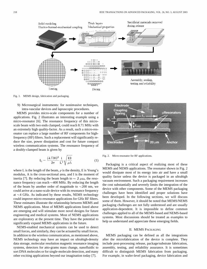
Fig. 1 illustrates a typical design and manufacturing processfor a MEMS device. This illustration highlights some of the dif-ferences between MEMS and microelectronics fabrication andpackaging. During the design, solid modeling is required since
Manuscript received July 3, 2003; revised July 8, 2003. This work was sup-ported in part by a project sponsored by the DARPA (Chip-scale atomic clockprogram), the Department of Interior (NBCH1020008), and a grant from theU.S. Department of Defense.
Y. C. Lee is with the Department of Mechanical Engineering, University ofColorado, Boulder, CO 80302 USA.
B. A. Parviz is with the Department of Chemistry and Chemical Biology,Harvard University, Cambridge, MA 02138 USA (e-mail: [email protected]).
J. A. Chiou is with the Motorola Inc., Deer Park, IL 60010 USA.S. Chen is with the Department of Mechanical Engineering, University of
Texas, Austin, TX 78712 USA.Digital Object Identifier 10.1109/TADVP.2003.817973
electro-thermal-mechanical coupling is essential to the func-tions of most of MEMS devices. The fabrication often involvesdeposition and etching of miron-thick layers with controlledmechanical and electrical properties [1], [2]. In many devices,after the completion of the fabrication process, the sacrificialmaterials are removed by etching in order to release the devicefor mechanical movements. This release process is usually thefirst step in the MEMS packaging. The released device shownin the figure represents a configuration for pressure sensors oraccelerometers or an element of an array for optical micro-mir-rors and RF switches. After release, the devices can be tested onthe wafer-level, followed by dicing. The released, diced deviceis assembled and sealed in a package. These testing, dicing, as-sembly and sealing steps are very challenging. Without properprotection, the micro-scale, movable features could be damagedeasily during these steps [3]. As a result, it is always desirableto replace the process illustrated here by wafer-level packaging[4].
Hundreds of MEMS-based sensors and actuators and systemshave been demonstrated and the number of their applications isgrowing. Few examples of their diverse applications are listedas follows [5].
1) Pressure sensors: for sensing manifold air pressure andfuel pressure to decrease emission and fuel consumption;for measuring blood pressure.
2) Inertial sensors: accelerometers for measuring accelera-tion for launching air bags; gyros for measuring angularvelocity to stabilize ride and to detect rollover.
3) Chemical micro sensors: for fast, disposable blood chem-istry analysis; gas sensors.
4) Optical MEMS: micromirrors for projection displays;optical switches for wavelength division multiplexswitches; attenuators or micro-devices for active align-ments for optical microsystems; micro-displays orpaper-thin, direct-view displays.
5) Radio frequency (RF) MEMS: micro-resonators forintegrated RF transceiver chips; RF switches for mil-limeter-wave systems.
6) Microfluidics MEMS: DNA hybridization arrays or sim-ilar lab-on-a-chips for biomedical and biochemical devel-opment, bio-analysis and diagnostic; printerheads for inkjet printing.
7) Power MEMS: on-chip power generation and energystorage for portable systems.
8) MEMS-based data storage: micro-positioning andtracking devices for magnetic, optical, thermal, oratomic force data tracks; micro-mirrors for optical beamsteering.
1521-3323/03$17.00 © 2003 IEEE
218 IEEE TRANSACTIONS ON ADVANCED PACKAGING, VOL. 26, NO. 3, AUGUST 2003
Fig. 1. MEMS design, fabrication and packaging.
9) Microsurgical instruments: for noninvasive techniques,intra-vascular devices and laprascopic procedures.
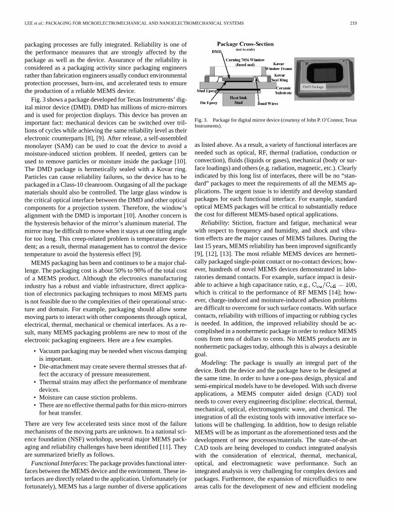
MEMS provides micro-scale components for a number ofapplications. Fig. 2 illustrates an interesting example using amicro-resonator [6]. The resonance frequency of this micro-scale beam with two ends clamped, could reach 8.71 MHz withan extremely high quality-factor. As a result, such a micro-res-onator can replace a large number of RF components for high-frequency (HF) filters. Such a replacement will significantly re-duce the size, power dissipation and cost for future compactwireless communication systems. The resonance frequency ofa doubly-clamped beam is given by
(1)
where L is the length of the beam,is the density, E is Young’smodulus, A is the cross-sectional area, and I is the moment ofinertia [7]. By reducing the beam length to , the reso-nance frequency can reach400 MHz. By reducing the lengthof the beam by another order of magnitude to200 nm, wecould arrive at a nano-scale device with its resonance frequencyat 4 GHz. As indicated by these results, NEMS technologycould improve micro-resonator applications for GHz RF filters.These estimates illustrate the relationship between MEMS andNEMS applications. Most of MEMS applications listed aboveare emerging and will stimulate more novel designs for futureengineering and medical systems. Most of NEMS applicationsare exploratory at the present time. They have the potential tosignificantly expand MEMS applications in the future.
NEMS-enabled mechanical systems can be used to detectsmall forces, and similarly, they can be actuated by small forces.In addition to the wireless communication, as mentioned above,NEMS technology may have an impact on ultrahigh-densitydata storage, molecular resolution magnetic resonance imagingsystems, detectors for atto-grams mass change, nanofluidic tosort DNA molecules or for single-molecule detection, and manyother exciting applications beyond our imagination today [7].
Fig. 2. Micro-resonator for RF applications.
Packaging is a critical aspect of realizing most of theseMEMS and NEMS applications. The resonator shown in Fig. 2would dissipate most of its energy into air and have a smallquality factor unless the device is packaged in an ultrahighvacuum environment. Such a packaging requirement increasesthe cost substantially and severely limits the integration of thedevice with other components. Some of the MEMS packagingchallenges have been identified and proper solutions havebeen developed. In the following sections, we will discusssome of them. However, it should be noted that MEMS/NEMSpackaging challenges are not fully understood and are usuallyapplication-dependent. It is impossible to define commonchallenges applied to all of the MEMS-based and NEMS-basedsystems. Most discussions should be treated as examples tohelp us understand and appreciate these emerging fields.
II. MEMS PACKAGING
MEMS packaging can be defined as all the integrationsafter the microfabrication of the device is complete. Theyinclude post-processing release, package/substrate fabrication,assembly, testing, and reliability assurance. It is sometimesdifficult to distinguish MEMS fabrication from packaging.For example, in wafer-level packaging, device fabrication and
LEE et al.: PACKAGING FOR MICROELECTROMECHANICAL AND NANOELECTROMECHANICAL SYSTEMS 219
packaging processes are fully integrated. Reliability is one ofthe performance measures that are strongly affected by thepackage as well as the device. Assurance of the reliability isconsidered as a packaging activity since packaging engineersrather than fabrication engineers usually conduct environmentalprotection processes, burn-ins, and accelerated tests to ensurethe production of a reliable MEMS device.
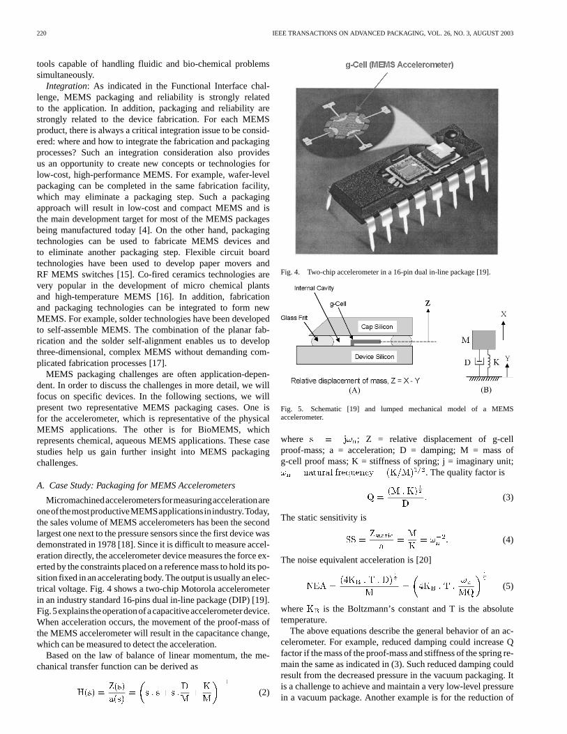
Fig. 3 shows a package developed for Texas Instruments’ dig-ital mirror device (DMD). DMD has millions of micro-mirrorsand is used for projection displays. This device has proven animportant fact: mechanical devices can be switched over tril-lions of cycles while achieving the same reliability level as theirelectronic counterparts [8], [9]. After release, a self-assembledmonolayer (SAM) can be used to coat the device to avoid amoisture-induced stiction problem. If needed, getters can beused to remove particles or moisture inside the package [10].The DMD package is hermetically sealed with a Kovar ring.Particles can cause reliability failures, so the device has to bepackaged in a Class-10 cleanroom. Outgasing of all the packagematerials should also be controlled. The large glass window isthe critical optical interface between the DMD and other opticalcomponents for a projection system. Therefore, the window’salignment with the DMD is important [10]. Another concern isthe hysteresis behavior of the mirror’s aluminum material. Themirror may be difficult to move when it stays at one titling anglefor too long. This creep-related problem is temperature depen-dent; as a result, thermal management has to control the devicetemperature to avoid the hysteresis effect [9].
MEMS packaging has been and continues to be a major chal-lenge. The packaging cost is about 50% to 90% of the total costof a MEMS product. Although the electronics manufacturingindustry has a robust and viable infrastructure, direct applica-tion of electronics packaging techniques to most MEMS partsis not feasible due to the complexities of their operational struc-ture and domain. For example, packaging should allow somemoving parts to interact with other components through optical,electrical, thermal, mechanical or chemical interfaces. As a re-sult, many MEMS packaging problems are new to most of theelectronic packaging engineers. Here are a few examples.
• Vacuum packaging may be needed when viscous dampingis important.
• Die-attachment may create severe thermal stresses that af-fect the accuracy of pressure measurement.
• Thermal strains may affect the performance of membranedevices.
• Moisture can cause stiction problems.• There are no effective thermal paths for thin micro-mirrors
for heat transfer.
There are very few accelerated tests since most of the failuremechanisms of the moving parts are unknown. In a national sci-ence foundation (NSF) workshop, several major MEMS pack-aging and reliability challenges have been identified [11]. Theyare summarized briefly as follows.
Functional Interfaces: The package provides functional inter-faces between the MEMS device and the environment. These in-terfaces are directly related to the application. Unfortunately (orfortunately), MEMS has a large number of diverse applications
Fig. 3. Package for digital mirror device (courtesy of John P. O’Connor, TexasInstruments).
as listed above. As a result, a variety of functional interfaces areneeded such as optical, RF, thermal (radiation, conduction orconvection), fluids (liquids or gases), mechanical (body or sur-face loadings) and others (e.g. radiation, magnetic, etc.). Clearlyindicated by this long list of interfaces, there will be no “stan-dard” packages to meet the requirements of all the MEMS ap-plications. The urgent issue is to identify and develop standardpackages for each functional interface. For example, standardoptical MEMS packages will be critical to substantially reducethe cost for different MEMS-based optical applications.
Reliability: Stiction, fracture and fatigue, mechanical wearwith respect to frequency and humidity, and shock and vibra-tion effects are the major causes of MEMS failures. During thelast 15 years, MEMS reliability has been improved significantly[9], [12], [13]. The most reliable MEMS devices are hermeti-cally packaged single-point contact or no-contact devices; how-ever, hundreds of novel MEMS devices demonstrated in labo-ratories demand contacts. For example, surface impact is desir-able to achieve a high capacitance ratio, e.g., ,which is critical to the performance of RF MEMS [14]; how-ever, charge-induced and moisture-induced adhesion problemsare difficult to overcome for such surface contacts. With surfacecontacts, reliability with trillions of impacting or rubbing cyclesis needed. In addition, the improved reliability should be ac-complished in a nonhermetic package in order to reduce MEMScosts from tens of dollars to cents. No MEMS products are innonhermetic packages today, although this is always a desirablegoal.
Modeling: The package is usually an integral part of thedevice. Both the device and the package have to be designed atthe same time. In order to have a one-pass design, physical andsemi-empirical models have to be developed. With such diverseapplications, a MEMS computer aided design (CAD) toolneeds to cover every engineering discipline: electrical, thermal,mechanical, optical, electromagnetic wave, and chemical. Theintegration of all the existing tools with innovative interface so-lutions will be challenging. In addition, how to design reliableMEMS will be as important as the aforementioned tests and thedevelopment of new processes/materials. The state-of-the-artCAD tools are being developed to conduct integrated analysiswith the consideration of electrical, thermal, mechanical,optical, and electromagnetic wave performance. Such anintegrated analysis is very challenging for complex devices andpackages. Furthermore, the expansion of microfluidics to newareas calls for the development of new and efficient modeling
220 IEEE TRANSACTIONS ON ADVANCED PACKAGING, VOL. 26, NO. 3, AUGUST 2003
tools capable of handling fluidic and bio-chemical problemssimultaneously.
Integration: As indicated in the Functional Interface chal-lenge, MEMS packaging and reliability is strongly relatedto the application. In addition, packaging and reliability arestrongly related to the device fabrication. For each MEMSproduct, there is always a critical integration issue to be consid-ered: where and how to integrate the fabrication and packagingprocesses? Such an integration consideration also providesus an opportunity to create new concepts or technologies forlow-cost, high-performance MEMS. For example, wafer-levelpackaging can be completed in the same fabrication facility,which may eliminate a packaging step. Such a packagingapproach will result in low-cost and compact MEMS and isthe main development target for most of the MEMS packagesbeing manufactured today [4]. On the other hand, packagingtechnologies can be used to fabricate MEMS devices andto eliminate another packaging step. Flexible circuit boardtechnologies have been used to develop paper movers andRF MEMS switches [15]. Co-fired ceramics technologies arevery popular in the development of micro chemical plantsand high-temperature MEMS [16]. In addition, fabricationand packaging technologies can be integrated to form newMEMS. For example, solder technologies have been developedto self-assemble MEMS. The combination of the planar fab-rication and the solder self-alignment enables us to developthree-dimensional, complex MEMS without demanding com-plicated fabrication processes [17].
MEMS packaging challenges are often application-depen-dent. In order to discuss the challenges in more detail, we willfocus on specific devices. In the following sections, we willpresent two representative MEMS packaging cases. One isfor the accelerometer, which is representative of the physicalMEMS applications. The other is for BioMEMS, whichrepresents chemical, aqueous MEMS applications. These casestudies help us gain further insight into MEMS packagingchallenges.
A. Case Study: Packaging for MEMS Accelerometers
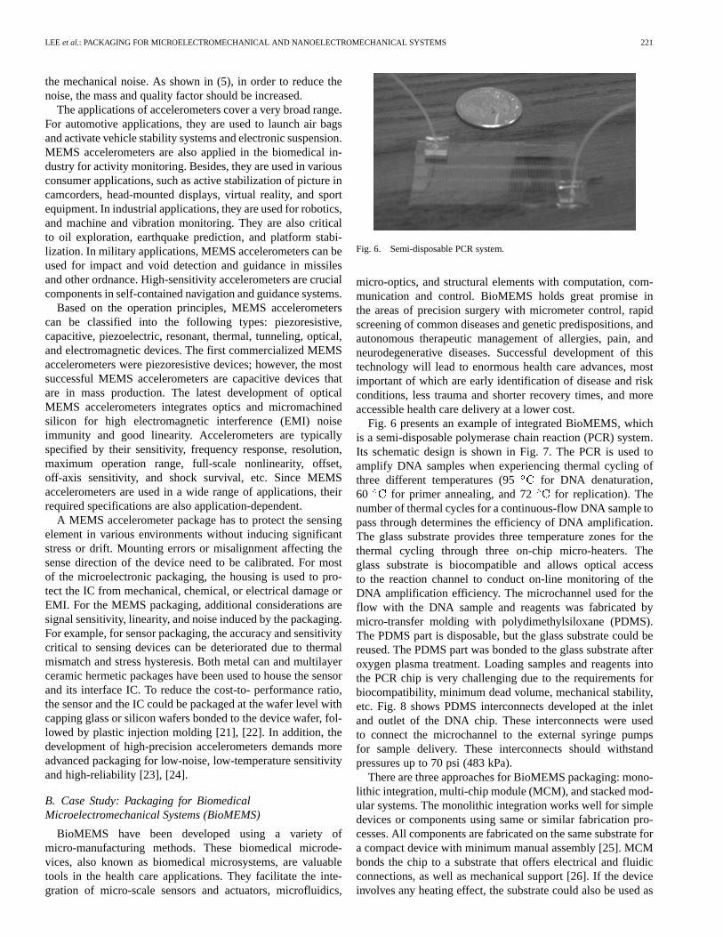
MicromachinedaccelerometersformeasuringaccelerationareoneofthemostproductiveMEMSapplicationsinindustry.Today,the sales volume of MEMS accelerometers has been the secondlargest one next to the pressure sensors since the first device wasdemonstrated in 1978 [18]. Since it is difficult to measure accel-eration directly, the accelerometer device measures the force ex-erted by the constraints placed on a reference mass to hold its po-sition fixed in an accelerating body. The output is usually an elec-trical voltage. Fig. 4 shows a two-chip Motorola accelerometerin an industry standard 16-pins dual in-line package (DIP) [19].Fig.5explainstheoperationofacapacitiveaccelerometerdevice.When acceleration occurs, the movement of the proof-mass ofthe MEMS accelerometer will result in the capacitance change,which can be measured to detect the acceleration.
Based on the law of balance of linear momentum, the me-chanical transfer function can be derived as
(2)
Fig. 4. Two-chip accelerometer in a 16-pin dual in-line package [19].
Fig. 5. Schematic [19] and lumped mechanical model of a MEMSaccelerometer.
where ; Z = relative displacement of g-cellproof-mass; a = acceleration; D = damping; M = mass ofg-cell proof mass; K = stiffness of spring; j = imaginary unit;
. The quality factor is
(3)
The static sensitivity is
(4)
The noise equivalent acceleration is [20]
(5)
where is the Boltzmann’s constant and T is the absolutetemperature.
The above equations describe the general behavior of an ac-celerometer. For example, reduced damping could increase Qfactor if the mass of the proof-mass and stiffness of the spring re-main the same as indicated in (3). Such reduced damping couldresult from the decreased pressure in the vacuum packaging. Itis a challenge to achieve and maintain a very low-level pressurein a vacuum package. Another example is for the reduction of
LEE et al.: PACKAGING FOR MICROELECTROMECHANICAL AND NANOELECTROMECHANICAL SYSTEMS 221
the mechanical noise. As shown in (5), in order to reduce thenoise, the mass and quality factor should be increased.
The applications of accelerometers cover a very broad range.For automotive applications, they are used to launch air bagsand activate vehicle stability systems and electronic suspension.MEMS accelerometers are also applied in the biomedical in-dustry for activity monitoring. Besides, they are used in variousconsumer applications, such as active stabilization of picture incamcorders, head-mounted displays, virtual reality, and sportequipment. In industrial applications, they are used for robotics,and machine and vibration monitoring. They are also criticalto oil exploration, earthquake prediction, and platform stabi-lization. In military applications, MEMS accelerometers can beused for impact and void detection and guidance in missilesand other ordnance. High-sensitivity accelerometers are crucialcomponents in self-contained navigation and guidance systems.
Based on the operation principles, MEMS accelerometerscan be classified into the following types: piezoresistive,capacitive, piezoelectric, resonant, thermal, tunneling, optical,and electromagnetic devices. The first commercialized MEMSaccelerometers were piezoresistive devices; however, the mostsuccessful MEMS accelerometers are capacitive devices thatare in mass production. The latest development of opticalMEMS accelerometers integrates optics and micromachinedsilicon for high electromagnetic interference (EMI) noiseimmunity and good linearity. Accelerometers are typicallyspecified by their sensitivity, frequency response, resolution,maximum operation range, full-scale nonlinearity, offset,off-axis sensitivity, and shock survival, etc. Since MEMSaccelerometers are used in a wide range of applications, theirrequired specifications are also application-dependent.
A MEMS accelerometer package has to protect the sensingelement in various environments without inducing significantstress or drift. Mounting errors or misalignment affecting thesense direction of the device need to be calibrated. For mostof the microelectronic packaging, the housing is used to pro-tect the IC from mechanical, chemical, or electrical damage orEMI. For the MEMS packaging, additional considerations aresignal sensitivity, linearity, and noise induced by the packaging.For example, for sensor packaging, the accuracy and sensitivitycritical to sensing devices can be deteriorated due to thermalmismatch and stress hysteresis. Both metal can and multilayerceramic hermetic packages have been used to house the sensorand its interface IC. To reduce the cost-to- performance ratio,the sensor and the IC could be packaged at the wafer level withcapping glass or silicon wafers bonded to the device wafer, fol-lowed by plastic injection molding [21], [22]. In addition, thedevelopment of high-precision accelerometers demands moreadvanced packaging for low-noise, low-temperature sensitivityand high-reliability [23], [24].
B. Case Study: Packaging for BiomedicalMicroelectromechanical Systems (BioMEMS)
BioMEMS have been developed using a variety ofmicro-manufacturing methods. These biomedical microde-vices, also known as biomedical microsystems, are valuabletools in the health care applications. They facilitate the inte-gration of micro-scale sensors and actuators, microfluidics,
Fig. 6. Semi-disposable PCR system.
micro-optics, and structural elements with computation, com-munication and control. BioMEMS holds great promise inthe areas of precision surgery with micrometer control, rapidscreening of common diseases and genetic predispositions, andautonomous therapeutic management of allergies, pain, andneurodegenerative diseases. Successful development of thistechnology will lead to enormous health care advances, mostimportant of which are early identification of disease and riskconditions, less trauma and shorter recovery times, and moreaccessible health care delivery at a lower cost.
Fig. 6 presents an example of integrated BioMEMS, whichis a semi-disposable polymerase chain reaction (PCR) system.Its schematic design is shown in Fig. 7. The PCR is used toamplify DNA samples when experiencing thermal cycling ofthree different temperatures (95 for DNA denaturation,60 for primer annealing, and 72 for replication). Thenumber of thermal cycles for a continuous-flow DNA sample topass through determines the efficiency of DNA amplification.The glass substrate provides three temperature zones for thethermal cycling through three on-chip micro-heaters. Theglass substrate is biocompatible and allows optical accessto the reaction channel to conduct on-line monitoring of theDNA amplification efficiency. The microchannel used for theflow with the DNA sample and reagents was fabricated bymicro-transfer molding with polydimethylsiloxane (PDMS).The PDMS part is disposable, but the glass substrate could bereused. The PDMS part was bonded to the glass substrate afteroxygen plasma treatment. Loading samples and reagents intothe PCR chip is very challenging due to the requirements forbiocompatibility, minimum dead volume, mechanical stability,etc. Fig. 8 shows PDMS interconnects developed at the inletand outlet of the DNA chip. These interconnects were usedto connect the microchannel to the external syringe pumpsfor sample delivery. These interconnects should withstandpressures up to 70 psi (483 kPa).
There are three approaches for BioMEMS packaging: mono-lithic integration, multi-chip module (MCM), and stacked mod-ular systems. The monolithic integration works well for simpledevices or components using same or similar fabrication pro-cesses. All components are fabricated on the same substrate fora compact device with minimum manual assembly [25]. MCMbonds the chip to a substrate that offers electrical and fluidicconnections, as well as mechanical support [26]. If the deviceinvolves any heating effect, the substrate could also be used as
222 IEEE TRANSACTIONS ON ADVANCED PACKAGING, VOL. 26, NO. 3, AUGUST 2003
Fig. 7. Schematic design of a semi-disposable PCR device developed byfabricating the microheaters on a glass substrate and the microchannel in adisposable PDMS cover sheet.
Fig. 8. PDMS-based micro-fluidic interconnect to deliver the DNA sampleand reagents to the PCR reaction channel.
a heat sink. The MCM approach offers excellent design flexi-bility and component-swapping capability. The stacked modularsystem involves individual components stacked to form a com-plicated integrated system. Its benefits include excellent flexi-bility, serviceability, and the possibility to test individual com-ponents and dispose a part of the system [27].
At the present time, only a small number of BioMEMS haveactually been used in real heath care applications. In addition toa slow approval process and the inertia of the medical industry,the technical barriers are packaging, materials, fluidics, inter-connects, reliability, testing, and calibration. The packagingchallenges are:
1) biocompatibility, requiring the device and packaging ma-terials not to be toxic to living cells;
2) temperature control, to prevent denaturation ofbiomolecules at high temperatures;
3) microfluidic, for device-to-device and device-to-macro-components interconnects;
4) electrical connections with isolation between electronicsand biofluids, to avoid signal interference and damage tothe biofluid;
5) disposability, to prevent transfer or interference of dis-eases. Any residual biomolecules from previous analysismay interfere with the current one and possibly transferdisease from one patient to another.
III. NEMS PACKAGING
As we mentioned in the introduction, exploration of NEMSfabrication technologies and applications is an active area of re-search among engineers and scientists across the globe. NEMStechnology has the potential to significantly expand the scope of
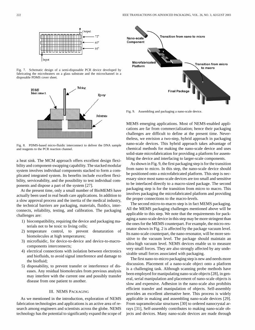
Fig. 9. Assembling and packaging a nano-scale device.
MEMS emerging applications. Most of NEMS-enabled appli-cations are far from commercialization; hence their packagingchallenges are difficult to define at the present time. Never-theless, we envision a two-step, hybrid approach in packagingnano-scale devices. This hybrid approach takes advantage ofchemical methods for making the nano-scale device and usessolid-state microfabrication for providing a platform for assem-bling the device and interfacing to larger-scale components.
As shown in Fig. 9, the first packaging step is for the transitionfrom nano to micro. In this step, the nano-scale device shouldbe positioned onto a microfabricated platform. This step is nec-essary since most nano-scale devices are too small and sensitiveto be interfaced directly to a macro-sized package. The secondpackaging step is for the transition from micro to macro. Thisinvolves packaging the microfabricated platform and providingthe proper connections to the macro-levels.
The second micro-to-macro step is in fact MEMS packaging.All the MEMS packaging challenges mentioned above will beapplicable to this step. We note that the requirements for pack-aging a nano-scale device in this step may be more stringent thanthe ones for the MEMS counterpart. For example, the micro-res-onator shown in Fig. 2 is affected by the package vacuum level.Its nano-scale counterpart, the nano-resonator, will be more sen-sitive to the vacuum level. The package should maintain anultra-high vacuum level. NEMS devices enable us to measurevery small forces. They are also strongly affected by any unde-sirable small forces associated with packaging.
The first nano-to-micro packaging step is new and needs morediscussion. Placement of a nano-scale object onto a platformis a challenging task. Although scanning probe methods havebeen employed for manipulating nano-scale objects [28], in gen-eral, serial manipulation and placement of nano-scale objects isslow and expensive. Adhesion in the nano-scale also prohibitsefficient transfer and manipulation of objects. Self-assemblyprovides an excellent alternative here. This process is widelyapplicable in making and assembling nano-scale devices [29].From supramolecular structures [30] to ordered nanocrystal ar-rays [31], Self-assembly contributes to making nano-scale ob-jects and devices. Many nano-scale devices are made through
LEE et al.: PACKAGING FOR MICROELECTROMECHANICAL AND NANOELECTROMECHANICAL SYSTEMS 223
synthetic chemical methods. For example, to make the propermolecule for a molecular electronics device, synthetic organicchemistry is used to make the molecule in the bulk form [32].After the molecules are made, self-assembly can assist in theproper placement of them onto a microfabricated platform.
Self-assembly is a highly parallel method and does notrequire one-by-one manipulation of components. In a self-as-sembly scheme, the nano-scale components are designed andproduced in such a fashion that they self-assemble in thecorrect position on the microfabricated platform spontaneously.Surface chemistry can be used to “program” such a self-as-sembly process. For example, thiol molecules in a molecularelectronics device self-assemble onto a gold platform due to thecovalent bond between the sulfur atoms in the molecules andthe gold atoms on the substrate [33]. This self-assembly processis “programmed” by placing the S-H group in the moleculesand providing a gold surface on the microfabricated platform.We anticipate that self-assembly will play a key role in thetransition from nano to micro step for packaging nano-scaledevices. Self-assembly at the molecular level provides a highlyparallel and precise way for manipulating components. Twocase studies will be presented to gain an insight into thisprocess.
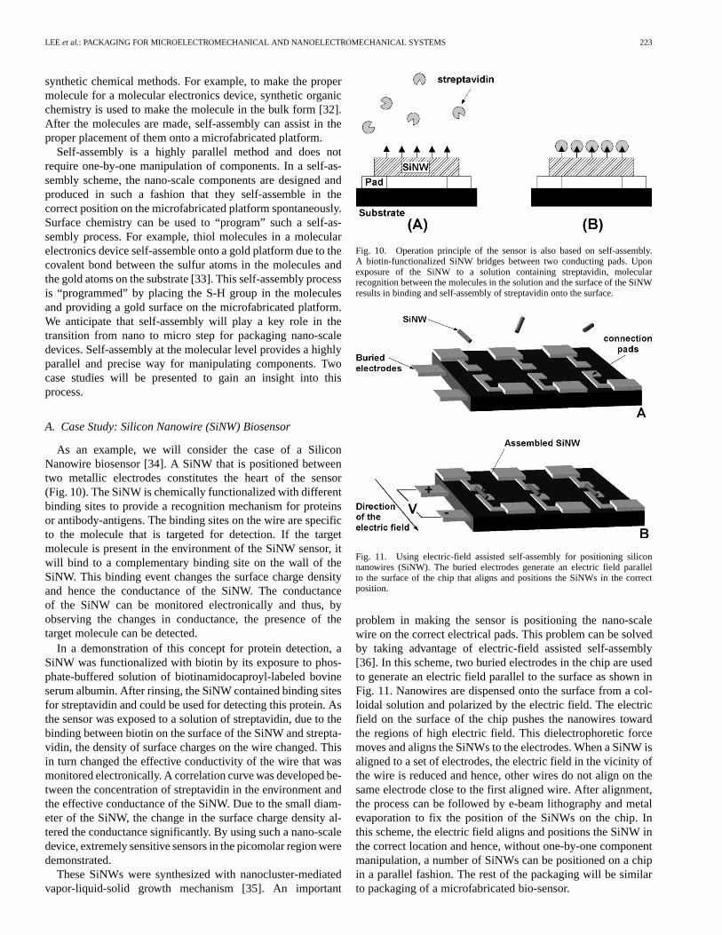
A. Case Study: Silicon Nanowire (SiNW) Biosensor
As an example, we will consider the case of a SiliconNanowire biosensor [34]. A SiNW that is positioned betweentwo metallic electrodes constitutes the heart of the sensor(Fig. 10). The SiNW is chemically functionalized with differentbinding sites to provide a recognition mechanism for proteinsor antibody-antigens. The binding sites on the wire are specificto the molecule that is targeted for detection. If the targetmolecule is present in the environment of the SiNW sensor, itwill bind to a complementary binding site on the wall of theSiNW. This binding event changes the surface charge densityand hence the conductance of the SiNW. The conductanceof the SiNW can be monitored electronically and thus, byobserving the changes in conductance, the presence of thetarget molecule can be detected.
In a demonstration of this concept for protein detection, aSiNW was functionalized with biotin by its exposure to phos-phate-buffered solution of biotinamidocaproyl-labeled bovineserum albumin. After rinsing, the SiNW contained binding sitesfor streptavidin and could be used for detecting this protein. Asthe sensor was exposed to a solution of streptavidin, due to thebinding between biotin on the surface of the SiNW and strepta-vidin, the density of surface charges on the wire changed. Thisin turn changed the effective conductivity of the wire that wasmonitored electronically. A correlation curve was developed be-tween the concentration of streptavidin in the environment andthe effective conductance of the SiNW. Due to the small diam-eter of the SiNW, the change in the surface charge density al-tered the conductance significantly. By using such a nano-scaledevice, extremely sensitive sensors in the picomolar region weredemonstrated.
These SiNWs were synthesized with nanocluster-mediatedvapor-liquid-solid growth mechanism [35]. An important
Fig. 10. Operation principle of the sensor is also based on self-assembly.A biotin-functionalized SiNW bridges between two conducting pads. Uponexposure of the SiNW to a solution containing streptavidin, molecularrecognition between the molecules in the solution and the surface of the SiNWresults in binding and self-assembly of streptavidin onto the surface.
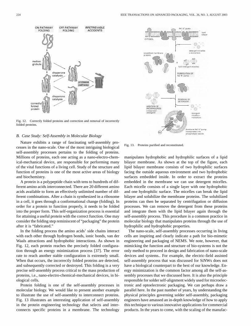
Fig. 11. Using electric-field assisted self-assembly for positioning siliconnanowires (SiNW). The buried electrodes generate an electric field parallelto the surface of the chip that aligns and positions the SiNWs in the correctposition.
problem in making the sensor is positioning the nano-scalewire on the correct electrical pads. This problem can be solvedby taking advantage of electric-field assisted self-assembly[36]. In this scheme, two buried electrodes in the chip are usedto generate an electric field parallel to the surface as shown inFig. 11. Nanowires are dispensed onto the surface from a col-loidal solution and polarized by the electric field. The electricfield on the surface of the chip pushes the nanowires towardthe regions of high electric field. This dielectrophoretic forcemoves and aligns the SiNWs to the electrodes. When a SiNW isaligned to a set of electrodes, the electric field in the vicinity ofthe wire is reduced and hence, other wires do not align on thesame electrode close to the first aligned wire. After alignment,the process can be followed by e-beam lithography and metalevaporation to fix the position of the SiNWs on the chip. Inthis scheme, the electric field aligns and positions the SiNW inthe correct location and hence, without one-by-one componentmanipulation, a number of SiNWs can be positioned on a chipin a parallel fashion. The rest of the packaging will be similarto packaging of a microfabricated bio-sensor.
224 IEEE TRANSACTIONS ON ADVANCED PACKAGING, VOL. 26, NO. 3, AUGUST 2003
Fig. 12. Correctly folded proteins and correction and removal of incorrectlyfolded proteins.
B. Case Study: Self-Assembly in Molecular Biology
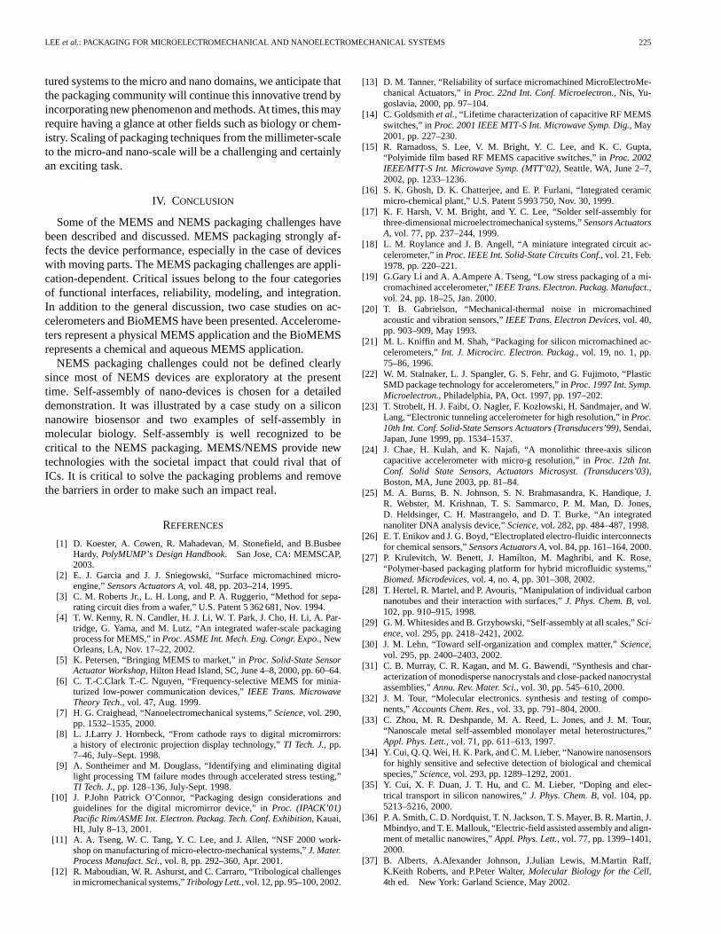
Nature exhibits a range of fascinating self-assembly pro-cesses in the nano-scale. One of the most intriguing biologicalself-assembly processes pertains to the folding of proteins.Millions of proteins, each one acting as a nano-electro-chem-ical-mechanical device, are responsible for performing manyof the vital functions of a living cell. Study of the structure andfunction of proteins is one of the most active areas of biologyand biochemistry.
A protein is a polypeptide chain with tens to hundreds of dif-ferent amino acids interconnected. There are 20 different aminoacids available to form an effectively unlimited number of dif-ferent combinations. After a chain is synthesized in a ribosomein a cell, it goes through a conformational change (folding). Inorder for a protein to function properly, it needs to be foldedinto the proper form. This self-organization process is essentialfor attaining a useful protein with the correct function. One mayconsider the folding step reminiscent of “packaging” the proteinafter it is “fabricated.”
In the folding process the amino acids’ side chains interactwith each other through hydrogen bonds, ionic bonds, van derWaals attractions and hydrophobic interactions. As shown inFig. 12, each protein reaches the precisely folded configura-tion through an energy minimization process [37]. The errorrate to reach another stable configuration is extremely small.When that occurs, the incorrectly folded proteins are detected,and subsequently corrected or destroyed. This folding is a veryprecise self-assembly process critical to the mass production ofproteins, i.e., nano-electro-chemical-mechanical devices, in bi-ological cells.
Protein folding is one of the self-assembly processes inmolecular biology. We would like to present another exampleto illustrate the use of self-assembly to interconnect proteins.Fig. 13 illustrates an interesting application of self-assemblyin the protein engineering technology that selects and inter-connects specific proteins in a membrane. The technology
Fig. 13. Proteins purified and reconstituted.
manipulates hydrophobic and hydrophilic surfaces of a lipidbilayer membrane. As shown at the top of the figure, eachlipid bilayer membrane consists of two hydrophilic surfacesfacing the outside aqueous environment and two hydrophobicsurfaces embedded inside. In order to extract the proteinsembedded in the membrane we can use detergent micelles.Each micelle consists of a single layer with one hydrophobicand one hydrophilic surface. The micelles can break the lipidbilayer and solubilize the membrane proteins. The solubilizedproteins can then be separated by centrifugation or diffusionprocesses. We can remove the detergent from these proteinsand integrate them with the lipid bilayer again through theself-assembly process. This procedure is a common practice inmolecular biology that manipulates proteins through the use ofhydrophilic and hydrophobic properties.
The nano-scale, self-assembly processes occurring in livingcells are inspiring and clearly indicate a path for bio-mimeticengineering and packaging of NEMS. We note, however, thatmimicking the function and structure of bio-systems is not theonly method to proceed in design and fabrication of nano-scaledevices and systems.. For example, the electric-field assistedself-assembly process that was discussed for SiNWs does nothave a biological counterpart to the best of our knowledge. En-ergy minimization is the common factor among all the self-as-sembly processes that we discussed here. It is also the principleresponsible for solder self-alignment widely used for microelec-tronic and optoelectronic packaging. We can perhaps draw aparallel here. In the past number of years, by understanding thephysical principles governing solder self-assembly, packagingengineers have amassed an in-depth knowledge of how to applythis technique to various innovative applications for commercialproducts. In the years to come, with the scaling of the manufac-
LEE et al.: PACKAGING FOR MICROELECTROMECHANICAL AND NANOELECTROMECHANICAL SYSTEMS 225
tured systems to the micro and nano domains, we anticipate thatthe packaging community will continue this innovative trend byincorporating new phenomenon and methods. At times, this mayrequire having a glance at other fields such as biology or chem-istry. Scaling of packaging techniques from the millimeter-scaleto the micro-and nano-scale will be a challenging and certainlyan exciting task.
IV. CONCLUSION
Some of the MEMS and NEMS packaging challenges havebeen described and discussed. MEMS packaging strongly af-fects the device performance, especially in the case of deviceswith moving parts. The MEMS packaging challenges are appli-cation-dependent. Critical issues belong to the four categoriesof functional interfaces, reliability, modeling, and integration.In addition to the general discussion, two case studies on ac-celerometers and BioMEMS have been presented. Accelerome-ters represent a physical MEMS application and the BioMEMSrepresents a chemical and aqueous MEMS application.
NEMS packaging challenges could not be defined clearlysince most of NEMS devices are exploratory at the presenttime. Self-assembly of nano-devices is chosen for a detaileddemonstration. It was illustrated by a case study on a siliconnanowire biosensor and two examples of self-assembly inmolecular biology. Self-assembly is well recognized to becritical to the NEMS packaging. MEMS/NEMS provide newtechnologies with the societal impact that could rival that ofICs. It is critical to solve the packaging problems and removethe barriers in order to make such an impact real.
REFERENCES
[1] D. Koester, A. Cowen, R. Mahadevan, M. Stonefield, and B.BusbeeHardy,PolyMUMP’s Design Handbook. San Jose, CA: MEMSCAP,2003.
[2] E. J. Garcia and J. J. Sniegowski, “Surface micromachined micro-engine,”Sensors Actuators A, vol. 48, pp. 203–214, 1995.
[3] C. M. Roberts Jr., L. H. Long, and P. A. Ruggerio, “Method for sepa-rating circuit dies from a wafer,” U.S. Patent 5 362 681, Nov. 1994.
[4] T. W. Kenny, R. N. Candler, H. J. Li, W. T. Park, J. Cho, H. Li, A. Par-tridge, G. Yama, and M. Lutz, “An integrated wafer-scale packagingprocess for MEMS,” inProc. ASME Int. Mech. Eng. Congr. Expo., NewOrleans, LA, Nov. 17–22, 2002.
[5] K. Petersen, “Bringing MEMS to market,” inProc. Solid-State SensorActuator Workshop, Hilton Head Island, SC, June 4–8, 2000, pp. 60–64.
[6] C. T.-C.Clark T.-C. Nguyen, “Frequency-selective MEMS for minia-turized low-power communication devices,”IEEE Trans. MicrowaveTheory Tech., vol. 47, Aug. 1999.
[7] H. G. Craighead, “Nanoelectromechanical systems,”Science, vol. 290,pp. 1532–1535, 2000.
[8] L. J.Larry J. Hornbeck, “From cathode rays to digital micromirrors:a history of electronic projection display technology,”TI Tech. J., pp.7–46, July–Sept. 1998.
[9] A. Sontheimer and M. Douglass, “Identifying and eliminating digitallight processing TM failure modes through accelerated stress testing,”TI Tech. J., pp. 128–136, July-Sept. 1998.
[10] J. P.John Patrick O’Connor, “Packaging design considerations andguidelines for the digital micromirror device,” inProc. (IPACK’01)Pacific Rim/ASME Int. Electron. Packag. Tech. Conf. Exhibition, Kauai,HI, July 8–13, 2001.
[11] A. A. Tseng, W. C. Tang, Y. C. Lee, and J. Allen, “NSF 2000 work-shop on manufacturing of micro-electro-mechanical systems,”J. Mater.Process Manufact. Sci., vol. 8, pp. 292–360, Apr. 2001.
[12] R. Maboudian, W. R. Ashurst, and C. Carraro, “Tribological challengesin micromechanical systems,”Tribology Lett., vol. 12, pp. 95–100, 2002.
[13] D. M. Tanner, “Reliability of surface micromachined MicroElectroMe-chanical Actuators,” inProc. 22nd Int. Conf. Microelectron., Nis, Yu-goslavia, 2000, pp. 97–104.
[14] C. Goldsmithet al., “Lifetime characterization of capacitive RF MEMSswitches,” inProc. 2001 IEEE MTT-S Int. Microwave Symp. Dig., May2001, pp. 227–230.
[15] R. Ramadoss, S. Lee, V. M. Bright, Y. C. Lee, and K. C. Gupta,“Polyimide film based RF MEMS capacitive switches,” inProc. 2002IEEE/MTT-S Int. Microwave Symp. (MTT’02), Seattle, WA, June 2–7,2002, pp. 1233–1236.
[16] S. K. Ghosh, D. K. Chatterjee, and E. P. Furlani, “Integrated ceramicmicro-chemical plant,” U.S. Patent 5 993 750, Nov. 30, 1999.
[17] K. F. Harsh, V. M. Bright, and Y. C. Lee, “Solder self-assembly forthree-dimensional microelectromechanical systems,”Sensors ActuatorsA, vol. 77, pp. 237–244, 1999.
[18] L. M. Roylance and J. B. Angell, “A miniature integrated circuit ac-celerometer,” inProc. IEEE Int. Solid-State Circuits Conf., vol. 21, Feb.1978, pp. 220–221.
[19] G.Gary Li and A. A.Ampere A. Tseng, “Low stress packaging of a mi-cromachined accelerometer,”IEEE Trans. Electron. Packag. Manufact.,vol. 24, pp. 18–25, Jan. 2000.
[20] T. B. Gabrielson, “Mechanical-thermal noise in micromachinedacoustic and vibration sensors,”IEEE Trans. Electron Devices, vol. 40,pp. 903–909, May 1993.
[21] M. L. Kniffin and M. Shah, “Packaging for silicon micromachined ac-celerometers,”Int. J. Microcirc. Electron. Packag., vol. 19, no. 1, pp.75–86, 1996.
[22] W. M. Stalnaker, L. J. Spangler, G. S. Fehr, and G. Fujimoto, “PlasticSMD package technology for accelerometers,” inProc. 1997 Int. Symp.Microelectron., Philadelphia, PA, Oct. 1997, pp. 197–202.
[23] T. Strobelt, H. J. Faibt, O. Nagler, F. Kozlowski, H. Sandmajer, and W.Lang, “Electronic tunneling accelerometer for high resolution,” inProc.10th Int. Conf. Solid-State Sensors Actuators (Transducers’99), Sendai,Japan, June 1999, pp. 1534–1537.
[24] J. Chae, H. Kulah, and K. Najafi, “A monolithic three-axis siliconcapacitive accelerometer with micro-g resolution,” inProc. 12th Int.Conf. Solid State Sensors, Actuators Microsyst. (Transducers’03),Boston, MA, June 2003, pp. 81–84.
[25] M. A. Burns, B. N. Johnson, S. N. Brahmasandra, K. Handique, J.R. Webster, M. Krishnan, T. S. Sammarco, P. M. Man, D. Jones,D. Heldsinger, C. H. Mastrangelo, and D. T. Burke, “An integratednanoliter DNA analysis device,”Science, vol. 282, pp. 484–487, 1998.
[26] E. T. Enikov and J. G. Boyd, “Electroplated electro-fluidic interconnectsfor chemical sensors,”Sensors Actuators A, vol. 84, pp. 161–164, 2000.
[27] P. Krulevitch, W. Benett, J. Hamilton, M. Maghribi, and K. Rose,“Polymer-based packaging platform for hybrid microfluidic systems,”Biomed. Microdevices, vol. 4, no. 4, pp. 301–308, 2002.
[28] T. Hertel, R. Martel, and P. Avouris, “Manipulation of individual carbonnanotubes and their interaction with surfaces,”J. Phys. Chem. B, vol.102, pp. 910–915, 1998.
[29] G. M. Whitesides and B. Grzybowski, “Self-assembly at all scales,”Sci-ence, vol. 295, pp. 2418–2421, 2002.
[30] J. M. Lehn, “Toward self-organization and complex matter,”Science,vol. 295, pp. 2400–2403, 2002.
[31] C. B. Murray, C. R. Kagan, and M. G. Bawendi, “Synthesis and char-acterization of monodisperse nanocrystals and close-packed nanocrystalassemblies,”Annu. Rev. Mater. Sci., vol. 30, pp. 545–610, 2000.
[32] J. M. Tour, “Molecular electronics. synthesis and testing of compo-nents,”Accounts Chem. Res., vol. 33, pp. 791–804, 2000.
[33] C. Zhou, M. R. Deshpande, M. A. Reed, L. Jones, and J. M. Tour,“Nanoscale metal self-assembled monolayer metal heterostructures,”Appl. Phys. Lett., vol. 71, pp. 611–613, 1997.
[34] Y. Cui, Q. Q. Wei, H. K. Park, and C. M. Lieber, “Nanowire nanosensorsfor highly sensitive and selective detection of biological and chemicalspecies,”Science, vol. 293, pp. 1289–1292, 2001.
[35] Y. Cui, X. F. Duan, J. T. Hu, and C. M. Lieber, “Doping and elec-trical transport in silicon nanowires,”J. Phys. Chem. B, vol. 104, pp.5213–5216, 2000.
[36] P. A. Smith, C. D. Nordquist, T. N. Jackson, T. S. Mayer, B. R. Martin, J.Mbindyo, and T. E. Mallouk, “Electric-field assisted assembly and align-ment of metallic nanowires,”Appl. Phys. Lett., vol. 77, pp. 1399–1401,2000.
[37] B. Alberts, A.Alexander Johnson, J.Julian Lewis, M.Martin Raff,K.Keith Roberts, and P.Peter Walter,Molecular Biology for the Cell,4th ed. New York: Garland Science, May 2002.
226 IEEE TRANSACTIONS ON ADVANCED PACKAGING, VOL. 26, NO. 3, AUGUST 2003
Y. C. Lee (M’92) is a Professor of mechanicalengineering and a faculty member of the NSF Centerfor Advanced Manufacturing and Packaging ofMicrowave, Optical and Digital Electronics (CAMP-mode), University of Colorado, Boulder. Prior tojoining the University in 1989, he was a Member ofTechnical Staff, AT&T Bell Laboratories, MurrayHill, NJ. He editedOptoelectronic Packaging(NewYork: Wiley, 1997) andManufacturing Challengesin Electronic Packaging (New York: Chapman& Hall, 1997). His research activities include
low-cost prototyping and thermal management of multichip modules, 3-Dpackaging, self-aligning soldering, fluxless or solderless flip-chip connec-tions, optoelectronics packaging, process control using fuzzy-logic models,microelectromechanical systems and protein integration for microsystems.
Dr. Lee received the Presidential Young Investigator (National ScienceFoundation, 1990), and the Outstanding Young Manufacturing Engineer Award(SME, 1992). He was the General Chair of ASME InterPACK’01. He is theAssociate Editor of theASME Journal of Electronic Packagingand a GuestEditor for the IEEE TRANSACTIONS ONADVANCED PACKAGING: SPECIAL ISSUE
ON MEMS/NEMS PACKAGING.
Babak Amir Parviz (S’94–M’01) received the B.S.degree in electrical engineering from the Sharif Uni-versity of Technology, Tehran, Iran, in 1995, and theM.S. degree in electrical engineering, the M.S. degreein physics, and the Ph.D. degree in electrical engi-neering from the University of Michigan, Ann Arbor,in 1997 and 2001, respectively.
From 2000 to 2001, he was with NanovationTechnologies, Inc. as a Device Designer andProduct Manager for MEMS-based integratedoptical switches. Since 2001, he has been with
the Department of Chemistry and Chemical Biology, Harvard University,Cambridge, MA, as a Postdoctoral Research Fellow. His areas of interest arenano- and microfabrication, organic electronics, and MEMS.
Dr. Parviz received the Bronze Medal from the 22nd International PhysicsOlympiad, the First Place Kharazmi Award, and the Distinguished AchievementAward from the Electrical Engineering Department, University of Michigan.
J. Albert Chiou received the Ph.D. degree inmechanical engineering from the University ofMinnesota, Minneapolis, in 1987.
He is a Distinguished Member of the TechnicalStaff, Sensors Division, Integrated ElectronicSystems Sector, Motorola Inc., Deer Park, IL.His areas of interest include MEMS, electronicpackaging, multiphysics computational mechanicsand measurement, engine components, medicaldevices, and civil and aerospace structures. He haspublications in the Society of Engineering Science,
ASME, IMAPS, theJournal of Computers and Structuresand theJournal ofElectronic Packaging.
Dr. Chiou received several awards and fellowships from universities, andbest paper awards, innovation awards, and recognition awards from Motorola,Inc. He is a member of the ASME and a Registered Professional Engineer. Hehas chaired several technical sessions and served as panelists for ASME andIMAPS, and co-edited several volumes of MEMS PROCEEDINGS. He was Tech-nical Program Chair of IMAPS MEMS Advanced Technology Workshop for2000 and 2001.
Shaochen Chen received the Ph.D. degree inmechanical engineering from the University ofCalifornia, Berkeley, in 1999.
Currently he is an Assistant Professor with theMechanical Engineering Department, Universityof Texas, Austin. His research interest lies inMEMS, laser materials processing, and thermal/fluidtransport in micro-and nano-systems. His researchapplications include microelectronics, biomedicalengineering, and life science.
Dr. Chen received the CAREER Award from theU.S. National Science Foundation in 2001 and the Outstanding Young Manu-facturing Engineer Award from the Society of Manufacturing Engineers in 2002.


![JOURNAL OF MICROELECTROMECHANICAL SYSTEMS, VOL. 15, …€¦ · genated alkylsiloxane monolayers such as octadecyltrichlorosilane (OTS). [1637] Index Terms—Microelectromechanical](https://img.pdfslide.us/doc/110x75/606226c6f2c83655de52c35d/journal-of-microelectromechanical-systems-vol-15-genated-alkylsiloxane-monolayers.jpg)
![Liquid Encapsulation Technology for Microelectromechanical ... · Liquid Encapsulation Technology for Microelectromechanical Systems Norihisa Miki ... [27]. Therefore, sealing with](https://img.pdfslide.us/doc/110x75/5ebd6745ad290220a7044b42/liquid-encapsulation-technology-for-microelectromechanical-liquid-encapsulation.jpg)