Embed Size (px)
Citation preview
PLA
ST
ICB
GA
Y PACKAGE
8.00 mm
ing ball
M0.05(.002)
ABC
151413121110987654321
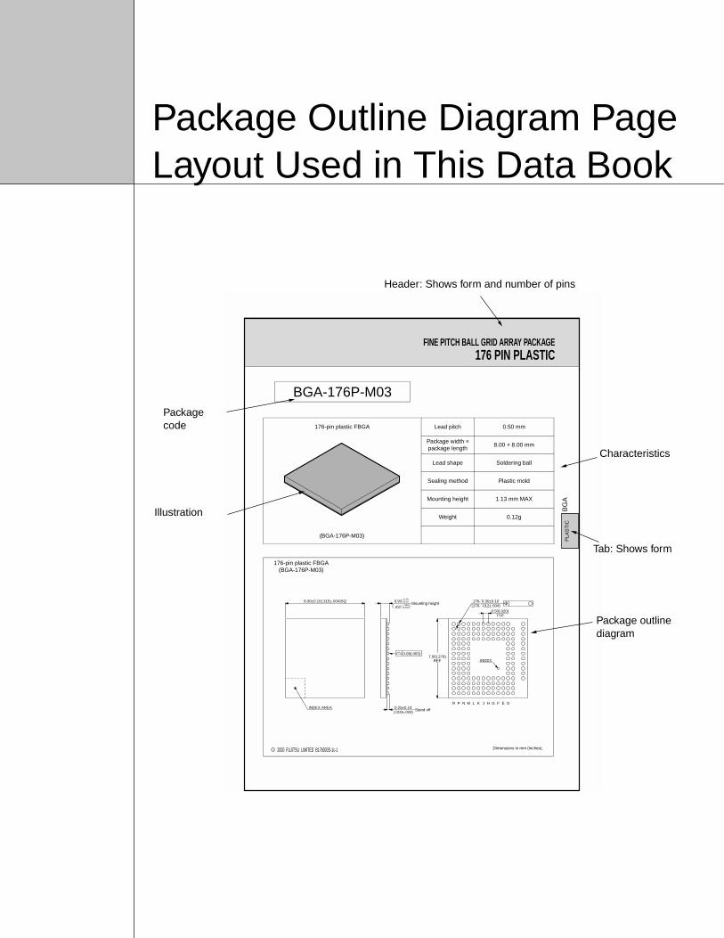
FINE PITCH BALL GRID ARRA176 PIN PLASTIC
176-pin plastic FBGA Lead pitch 0.50 mm
Package width × package length
8.00 ×
Lead shape Solder
Sealing method Plastic mold
Mounting height 1.13 mm MAX
Weight 0.12g
176-pin plastic FBGA(BGA-176P-M03)
(BGA-176P-M03)
C 2000 FUJITSU LIMITED B176003S-1c-1
8.00±0.10(.315±.004)SQ
INDEX
INDEX AREA
.037 Ð.004+.008
Ð0.10+0.20
0.93Mounting height
0.25±0.10(.010±.004)
Stand off
0.08(.003)7.00(.276)
REF
0.50(.020)TYP
176-¯0.30±0.10(176-¯.012±.004)
DEFGHJKLMNPR
Dimensions in mm (inches).
BGA-176P-M03
Header: Shows form and number of pins
Packagecode
Illustration
Characteristics
Tab: Shows form
Package outlinediagram
Package Outline Diagram PageLayout Used in This Data Book
1.1 Overview...................................................................................................... 3
1.2 Package Lineup .......................................................................................... 4
1.3 Package Forms
1.3.1 Lead insertion types .......................................................................... 6
1.3.2 Surface mounted types...................................................................... 6
1.4 Package Structures
1.4.1 Structure diagrams ............................................................................ 8
1.4.2 Sample Assembly Process.............................................................. 11
1.4.3 Structural materials ......................................................................... 13
1.4.4 Lead-Free Packages........................................................................ 15
1.5 How Package Dimensions Are Indicated
1.5.1 SOP dimensions.............................................................................. 16
1.6 Package Codes
1.6.1 Fujitsu Code Labeling...................................................................... 18
1.7 Marking
1.7.1 Standard marking ............................................................................ 20
1.7.2 Customer-specified marking............................................................ 21
1.8 Future Trends in Packages
1.8.1 Diversification .................................................................................. 22
1.8.2 Future formats ................................................................................. 22
1.8.3 Custom packages............................................................................ 23
1.8.4 Modules........................................................................................... 23
Introduction to Packages1

Package Structures
11
Intro
duct
ion
to P
acka
ges
1.1 Overview
Fujitsu provides semiconductor packages as a kind of "interposers" for protecting semiconductordevices and getting the full benefit of them. Fujitsu has developed and released a diversi-fied seriesof "general-purpose package families" supporting a wide range of applications to suit customers’needs. The packages include through-hole type packages such as DIPs and PGAs; QFPs andSOPs that contributed to setting the trend of surface mounting; and multi-pin QFPs, TCPs, andBGAs supporting high-tensity mounting.
In addition, Fujitsu has developed and provided custom packages, cards, and modules for specificcustomers.
This chapter begins with Fujitsu’s package lineup, followed by descriptions of package shapes andstructures.
This chapter also describes the package dimension display conventions based on the JEITA andJEDEC *1 standards to help you use this data book more efficiently as a source of information foryou.
Also, this chapter introduces Fujitsu’s basic concept of package development for future packages.
The electronic device marketplace has been demanding more advanced and diversified high-density mounting technologies.
Fujitsu has developed new packages (supporting CSP) to meet the needs of the industry. Tosupport customers for easier use of these new packages, at the same time, Fujitsu has made astrong commitment to standardization of the packages by JEITA *2 .
*1: Joint Electron Device Engineering Council
*2: Japan Electronics & Information Technology Industries Association
Package Structures
12
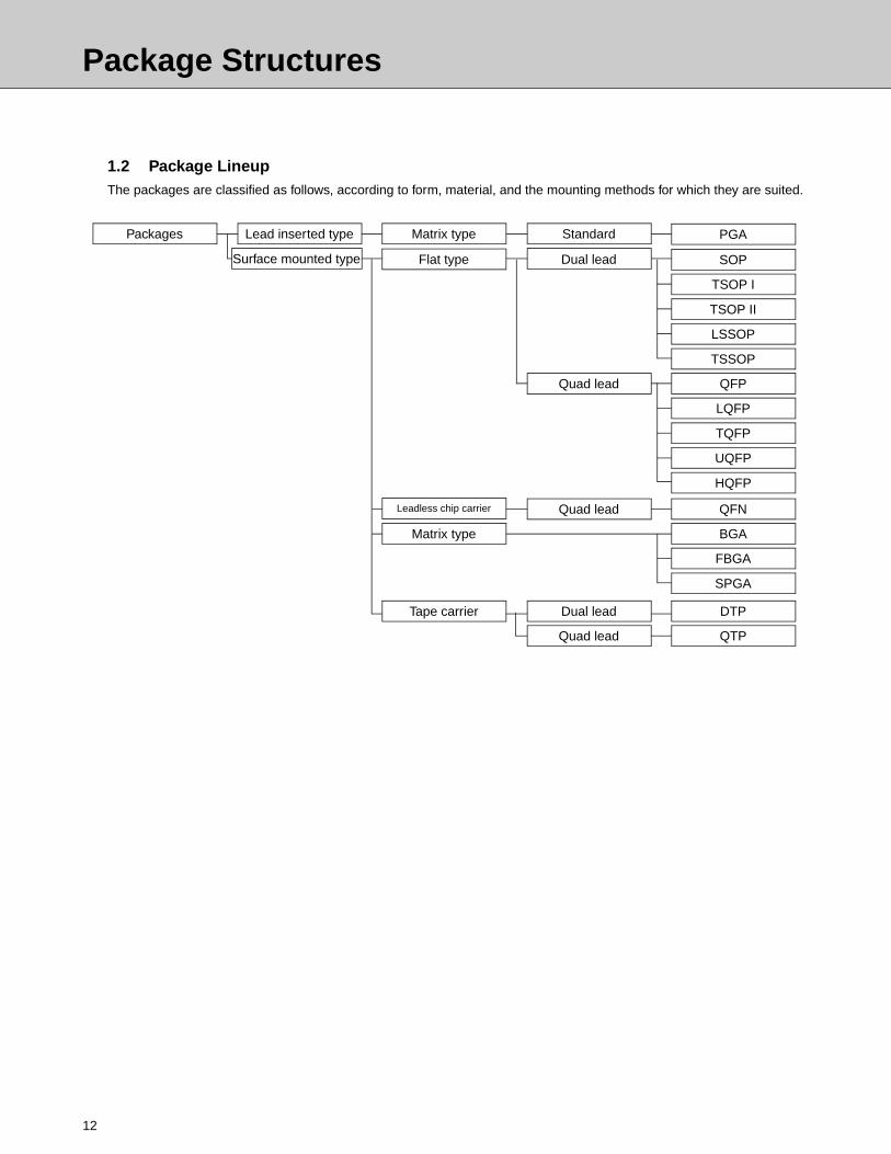
1.2 Package LineupThe packages are classified as follows, according to form, material, and the mounting methods for which they are suited.
Packages Lead inserted type PGA
SOP
TSOP I
TSOP II
LSSOP
TSSOP
QFP
LQFP
TQFP
UQFP
HQFP
QFN
BGA
SPGA
DTP
QTP
Standard
Dual lead
Quad lead
Quad lead
Dual lead
Quad lead
Matrix type
Flat typeSurface mounted type
Leadless chip carrier
Matrix type
Tape carrier
FBGA
Package Structures
11
Intro
duct
ion
to P
acka
ges
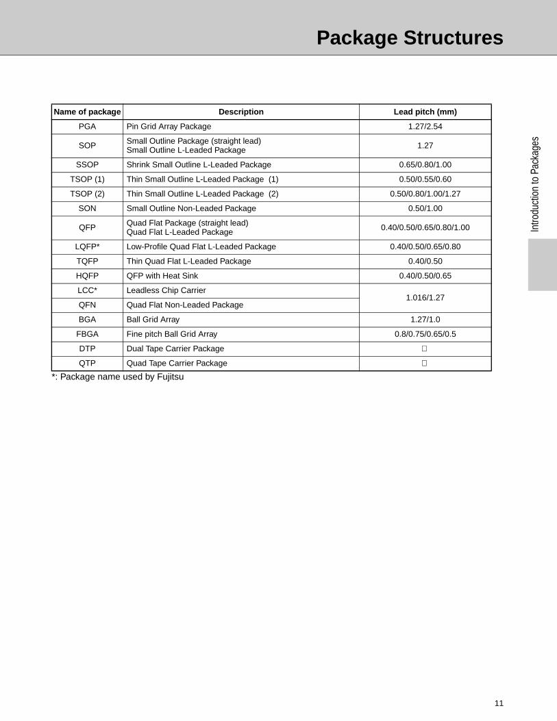
*: Package name used by Fujitsu
Name of package Description Lead pitch (mm)
PGA Pin Grid Array Package 1.27/2.54
SOP Small Outline Package (straight lead)Small Outline L-Leaded Package 1.27
SSOP Shrink Small Outline L-Leaded Package 0.65/0.80/1.00
TSOP (1) Thin Small Outline L-Leaded Package (1) 0.50/0.55/0.60
TSOP (2) Thin Small Outline L-Leaded Package (2) 0.50/0.80/1.00/1.27
SON Small Outline Non-Leaded Package 0.50/1.00
QFP Quad Flat Package (straight lead)Quad Flat L-Leaded Package 0.40/0.50/0.65/0.80/1.00
LQFP* Low-Profile Quad Flat L-Leaded Package 0.40/0.50/0.65/0.80
TQFP Thin Quad Flat L-Leaded Package 0.40/0.50
HQFP QFP with Heat Sink 0.40/0.50/0.65
LCC* Leadless Chip Carrier1.016/1.27
QFN Quad Flat Non-Leaded Package
BGA Ball Grid Array 1.27/1.0
FBGA Fine pitch Ball Grid Array 0.8/0.75/0.65/0.5
DTP Dual Tape Carrier Package
QTP Quad Tape Carrier Package
Package Structures
12
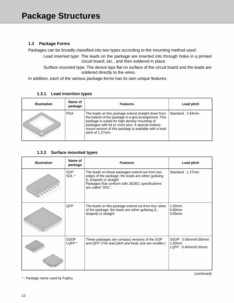
1.3 Package Forms
Packages can be broadly classified into two types according to the mounting method used:
Lead inserted type: The leads on the package are inserted into through holes in a printedcircuit board, etc., and then soldered in place.
Surface mounted type: The device lays flat on surface of the circuit board and the leads aresoldered directly to the wires.
In addition, each of the various package forms has its own unique features.
1.3.1 Lead insertion types
1.3.2 Surface mounted types
(continued)* : Package name used by Fujitsu.
IllustrationName of package
Features Lead pitch
PGA The leads on this package extend straight down from the bottom of the package in a grid arrangement. This package is suited for high-density mounting of packages with 64 or more pins. A special surface-mount version of this package is available with a lead pitch of 1.27mm.
Standard : 2.54mm
IllustrationName of package
Features Lead pitch
SOPSOL *
The leads on these packages extend out from two edges of the package; the leads are either gullwing (L-shaped) or straight.Packages that conform with JEDEC specifications are called "SOL".
Standard : 1.27mm
QFP The leads on this package extend out from four sides of the package; the leads are either gullwing (L-shaped) or straight.
1.00mm0.80mm0.65mm
SSOPLQFP *
These packages are compact versions of the SOP and QFP. (The lead pitch and body size are smaller.)
SSOP : 0.65mm/0.80mm/1.00mmLQFP : 0.40mm/0.50mm
Package Structures
11
Intro
duct
ion
to P
acka
ges
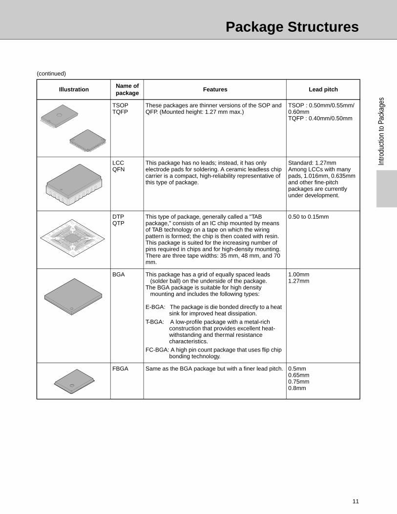
(continued)
IllustrationName of package
Features Lead pitch
TSOPTQFP
These packages are thinner versions of the SOP and QFP. (Mounted height: 1.27 mm max.)
TSOP : 0.50mm/0.55mm/0.60mmTQFP : 0.40mm/0.50mm
LCCQFN
This package has no leads; instead, it has only electrode pads for soldering. A ceramic leadless chip carrier is a compact, high-reliability representative of this type of package.
Standard: 1.27mmAmong LCCs with many pads, 1.016mm, 0.635mm and other fine-pitch packages are currently under development.
DTPQTP
This type of package, generally called a "TAB package," consists of an IC chip mounted by means of TAB technology on a tape on which the wiring pattern is formed; the chip is then coated with resin. This package is suited for the increasing number of pins required in chips and for high-density mounting. There are three tape widths: 35 mm, 48 mm, and 70 mm.
0.50 to 0.15mm
BGA This package has a grid of equally spaced leads (solder ball) on the underside of the package.
The BGA package is suitable for high density mounting and includes the following types:
E-BGA: The package is die bonded directly to a heat sink for improved heat dissipation.
T-BGA: A low-profile package with a metal-rich construction that provides excellent heat-withstanding and thermal resistance characteristics.
FC-BGA: A high pin count package that uses flip chip bonding technology.
1.00mm1.27mm
FBGA Same as the BGA package but with a finer lead pitch. 0.5mm0.65mm0.75mm0.8mm
JAPAN
160-01
Package Structures
12
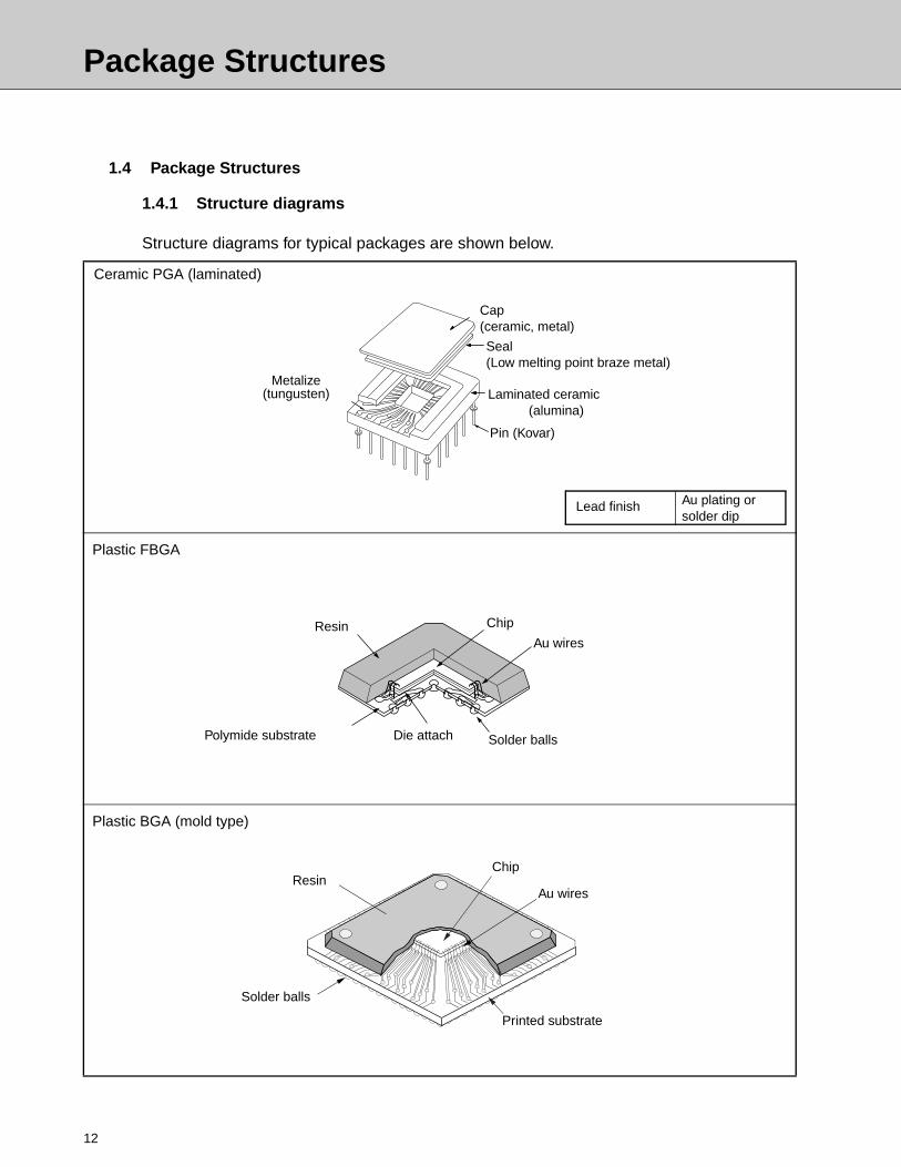
1.4 Package Structures
1.4.1 Structure diagrams
Structure diagrams for typical packages are shown below.
Ceramic PGA (laminated)
Pin (Kovar)
Laminated ceramic(alumina)
Metalize(tungusten)
Cap(ceramic, metal)
Seal(Low melting point braze metal)
Lead finish Au plating or solder dip
Plastic FBGA
Polymide substrate Solder ballsDie attach
Resin Chip
Au wires
Plastic BGA (mold type)
Resin
Solder balls
Chip
Au wires
Printed substrate
Package Structures
11
Intro
duct
ion
to P
acka
ges
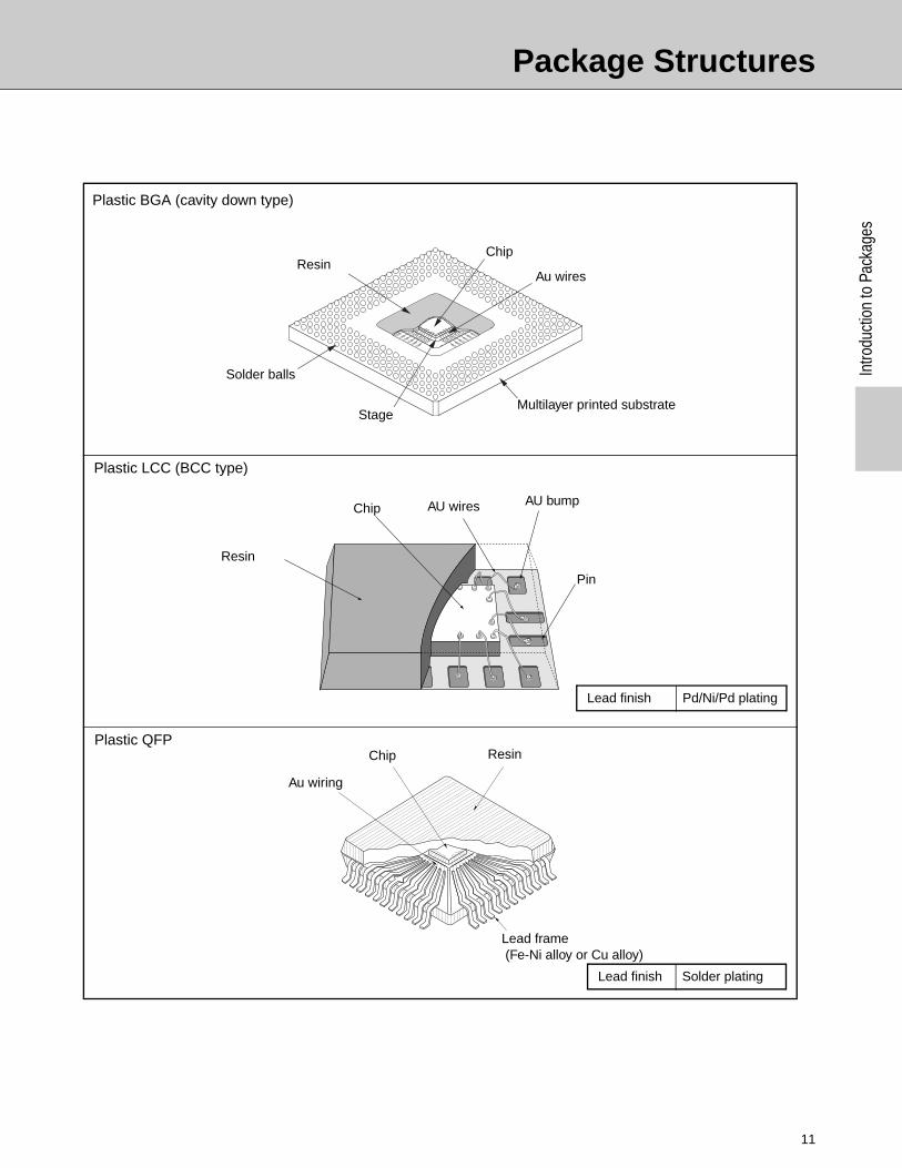
Plastic BGA (cavity down type)
ResinChip
Au wires
Solder balls
StageMultilayer printed substrate
Plastic LCC (BCC type)
Resin
Chip AU wires AU bump
Pin
Lead finish Pd/Ni/Pd plating
Plastic QFP
Au wiring
ResinChip
Lead frame (Fe-Ni alloy or Cu alloy)
Lead finish Solder plating
Package Structures
12
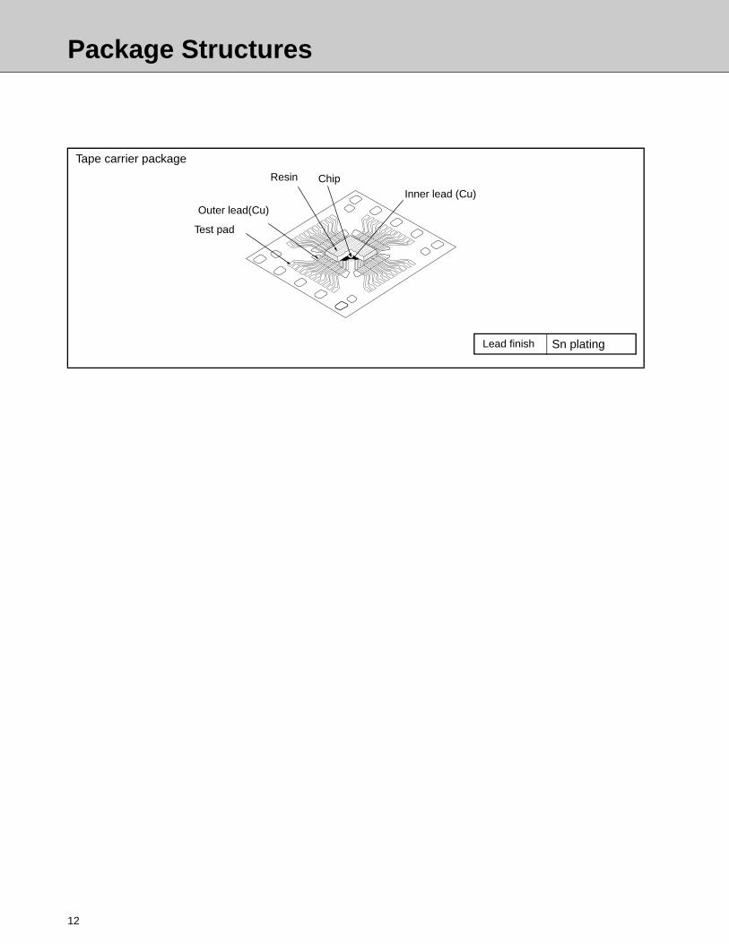
Tape carrier package
ChipResin
Outer lead(Cu)
Test pad
Inner lead (Cu)
Lead finish Sn plating
Package Structures
11
Intro
duct
ion
to P
acka
ges
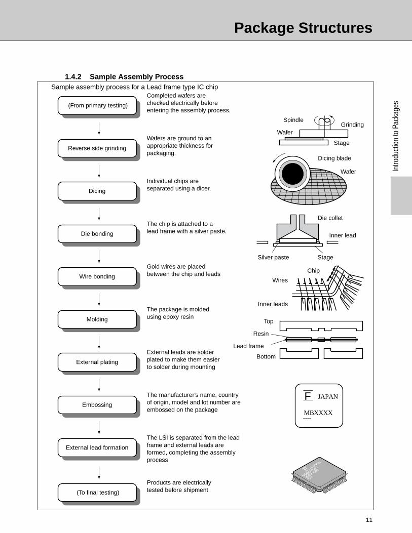
1.4.2 Sample Assembly Process
F JAPAN
MBXXXX
Sample assembly process for a Lead frame type IC chipCompleted wafers are checked electrically before entering the assembly process.
Wafers are ground to an appropriate thickness for packaging.
Individual chips are separated using a dicer.
The chip is attached to a lead frame with a silver paste.
Gold wires are placed between the chip and leads
The package is molded using epoxy resin
External leads are solder plated to make them easier to solder during mounting
The manufacturer’s name, country of origin, model and lot number are embossed on the package
The LSI is separated from the lead frame and external leads are formed, completing the assembly process
Products are electrically tested before shipment
(From primary testing)
Reverse side grinding
Dicing
Die bonding
Wire bonding
Molding
External plating
Embossing
External lead formation
(To final testing)
Spindle
WaferGrinding
Stage
Dicing blade
Wafer
Die collet
Inner lead
StageSilver paste
Chip
Wires
Inner leads
Resin
Lead frame
Top
Bottom
Package Structures
12
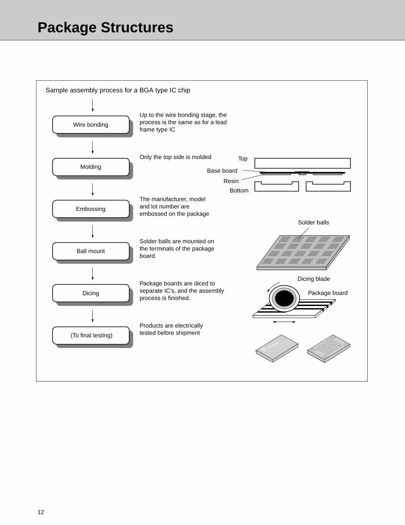
Sample assembly process for a BGA type IC chip
Up to the wire bonding stage, the process is the same as for a lead frame type IC
Only the top side is molded
The manufacturer, model and lot number are embossed on the package
Solder balls are mounted on the terminals of the package board
Package boards are diced to separate IC’s, and the assembly process is finished.
Products are electrically tested before shipment
Wire bonding
Molding
Embossing
Ball mount
Dicing
(To final testing)
Top
Bottom
Resin
Base board
Solder balls
Dicing blade
Package board
Package Structures
11
Intro
duct
ion
to P
acka
ges
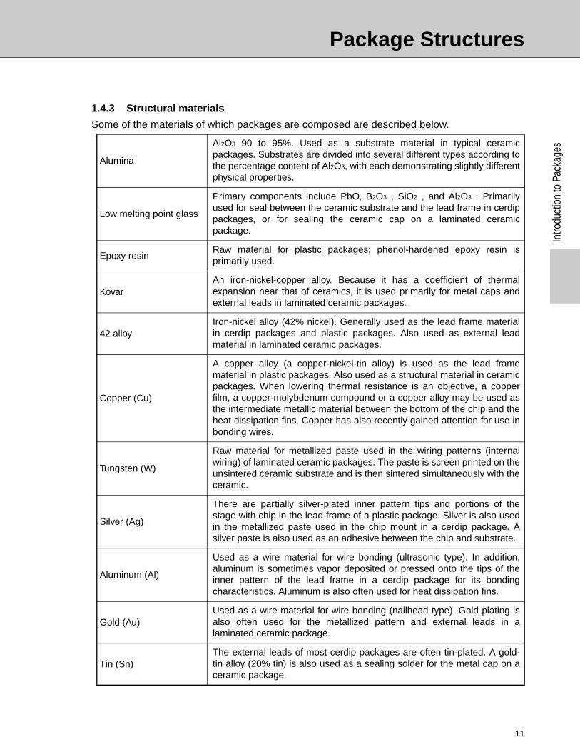
1.4.3 Structural materials
Some of the materials of which packages are composed are described below.
Alumina
Al2O3 90 to 95%. Used as a substrate material in typical ceramicpackages. Substrates are divided into several different types according tothe percentage content of Al2O3, with each demonstrating slightly differentphysical properties.
Low melting point glass
Primary components include PbO, B2O3 , SiO2 , and Al2O3 . Primarilyused for seal between the ceramic substrate and the lead frame in cerdippackages, or for sealing the ceramic cap on a laminated ceramicpackage.
Epoxy resinRaw material for plastic packages; phenol-hardened epoxy resin isprimarily used.
KovarAn iron-nickel-copper alloy. Because it has a coefficient of thermalexpansion near that of ceramics, it is used primarily for metal caps andexternal leads in laminated ceramic packages.
42 alloyIron-nickel alloy (42% nickel). Generally used as the lead frame materialin cerdip packages and plastic packages. Also used as external leadmaterial in laminated ceramic packages.
Copper (Cu)
A copper alloy (a copper-nickel-tin alloy) is used as the lead framematerial in plastic packages. Also used as a structural material in ceramicpackages. When lowering thermal resistance is an objective, a copperfilm, a copper-molybdenum compound or a copper alloy may be used asthe intermediate metallic material between the bottom of the chip and theheat dissipation fins. Copper has also recently gained attention for use inbonding wires.
Tungsten (W)
Raw material for metallized paste used in the wiring patterns (internalwiring) of laminated ceramic packages. The paste is screen printed on theunsintered ceramic substrate and is then sintered simultaneously with theceramic.
Silver (Ag)
There are partially silver-plated inner pattern tips and portions of thestage with chip in the lead frame of a plastic package. Silver is also usedin the metallized paste used in the chip mount in a cerdip package. Asilver paste is also used as an adhesive between the chip and substrate.
Aluminum (Al)
Used as a wire material for wire bonding (ultrasonic type). In addition,aluminum is sometimes vapor deposited or pressed onto the tips of theinner pattern of the lead frame in a cerdip package for its bondingcharacteristics. Aluminum is also often used for heat dissipation fins.
Gold (Au)Used as a wire material for wire bonding (nailhead type). Gold plating isalso often used for the metallized pattern and external leads in alaminated ceramic package.
Tin (Sn)The external leads of most cerdip packages are often tin-plated. A gold-tin alloy (20% tin) is also used as a sealing solder for the metal cap on aceramic package.
Package Structures
12
Lead-tin (solder)
A variety of solders with differing characteristics can be obtained bychanging the ratio of lead-tin composition. At present, lead-tin amalgamsolders (normally called solder plating) are used for external leadprocessing of plastic packages. Also used for sealing metal caps onceramic packages. In addition, used for solder dip processes for externalleads.
Tin-bismuth (solder) A lead-free solder, used for external lead processing of plastic packagesin lead-free mounting operation.
Tin-silver-copper (solder) A lead-free solder, used for solder balls on BGA packages.
Polyimide tape
This is the primary material in the tape used for TCP. This tape isgenerally made from pyromellitic dianhydride and aromatic diamine. Inaddition to the ability to withstand high temperatures, this tape alsopossesses excellent mechanical, electrical, and chemical characteristics.
Package Structures
11
Intro
duct
ion
to P
acka
ges
1.4.4 Lead-Free Packages
The use of lead-free electronic components is mentioned as a significant issue in global
environment assessments.
Lead is a harmful heavy metal, which if absorbed and accumulated in the body is reported to
cause damage including inhibited growth in children and psychological damage in adults.
In particular, lead can leach from electronic products that have been disposed of in land fills,
from contact with acid rainwater. This can lead to contamination of rivers and ground water,
and can thereby enter the body through drinking water.
At Fujitsu, we have actively addressed this problem by starting the production of lead-free
products with semiconductor packages completely free of lead as of October, 2000.
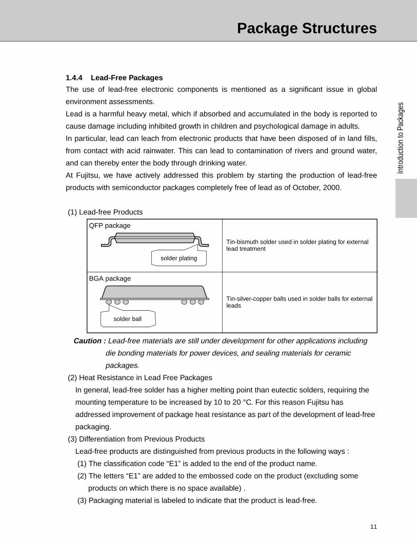
(1) Lead-free Products
Caution : Lead-free materials are still under development for other applications including
die bonding materials for power devices, and sealing materials for ceramic
packages.
(2) Heat Resistance in Lead Free Packages
In general, lead-free solder has a higher melting point than eutectic solders, requiring the
mounting temperature to be increased by 10 to 20 °C. For this reason Fujitsu has
addressed improvement of package heat resistance as part of the development of lead-free
packaging.
(3) Differentiation from Previous Products
Lead-free products are distinguished from previous products in the following ways :
(1) The classification code “E1” is added to the end of the product name.
(2) The letters “E1” are added to the embossed code on the product (excluding some
products on which there is no space available) .
(3) Packaging material is labeled to indicate that the product is lead-free.
QFP package
Tin-bismuth solder used in solder plating for external lead treatment
BGA package
Tin-silver-copper balls used in solder balls for external leads
solder plating
solder ball
Package Structures
12
1.5 How Package Dimensions Are Indicated
This section will use representative SOP package to explain the manner in which dimensions areindicated in the package outline dimension diagrams in this data book.
1.5.1 SOP dimensions
Dimension name Symbol Explanation
Mounting height A Height from the mounting surface to the top of the package
Standoff height A1 Distance between the mounting surface and the bottom of the package
Height of body A2 Thickness of the package (height of the body)
Pin width b Width of the pin (width between 0.1 and 0.25 mm from the tip)
Pin thickness c Thickness of the pin
Package length DThe longest dimension of the body of the package parallel to themounting surface and excluding the pins; also include resin burrs
Package width E The width of the body of the package, excluding the pins
Pin linear spacingLinear spacing between the centers of the pins; also called the "leadpitch"
Call dimension
Distance between the centers of the pads where the package ismounted; in the case of flat packages, there are generally four standardvalues:TYPE I : 5.72mm ( 225mil) TYPE II : 7.62mm ( 300mil) TYPE III : 9.53mm ( 375mil) TYPE IV : 11.43mm (450mil) TYPE V : 13.34mm (525mil) TYPE VI : 15.24mm (600mil)
Overall width HEDistance from the tip of one pin to the tip of the pin on the opposite sideof the package
Length of flat portion ofpin
LLength of the flat portion of the pin that comes into contact with themounting pad
Angle of flat portion of pin θ Angle formed by the mounting surface and the flat portion of the pin
Overhang ZDistance from the center position of an end pin to the end of the body ofthe package
X
q
Z e e
n n-1
E
A1 CZe e
y
e1L L
A2 A
1 2
D
Mφ
HE
bMounting plane
e
e1
e1
Package Structures
11
Intro
duct
ion
to P
acka
ges
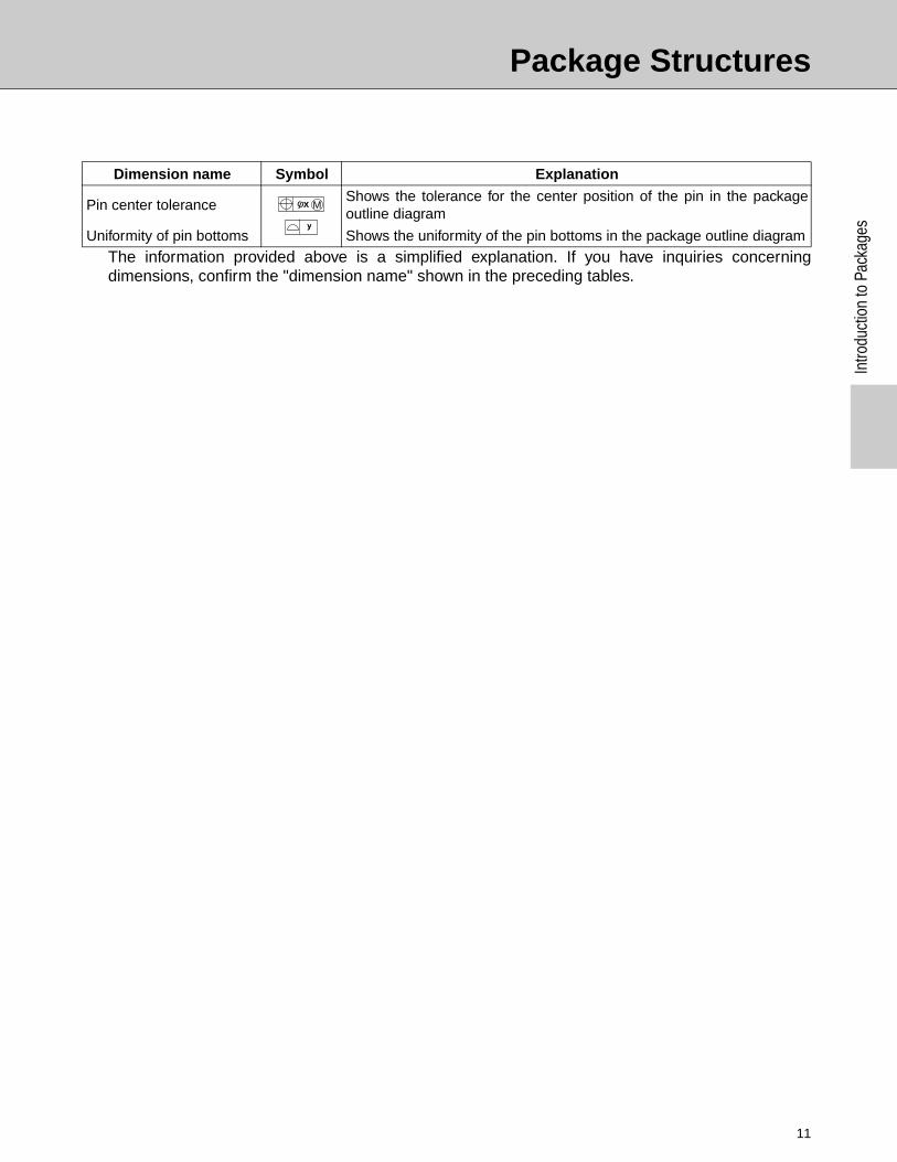
The information provided above is a simplified explanation. If you have inquiries concerningdimensions, confirm the "dimension name" shown in the preceding tables.
Pin center toleranceShows the tolerance for the center position of the pin in the packageoutline diagram
Uniformity of pin bottoms Shows the uniformity of the pin bottoms in the package outline diagram
Dimension name Symbol Explanation
X
y
Mφ
Package Structures
12
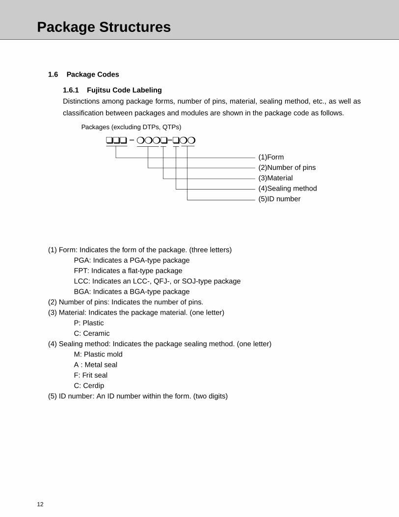
1.6 Package Codes
1.6.1 Fujitsu Code Labeling
Distinctions among package forms, number of pins, material, sealing method, etc., as well as
classification between packages and modules are shown in the package code as follows.
(1) Form: Indicates the form of the package. (three letters)
PGA: Indicates a PGA-type package
FPT: Indicates a flat-type package
LCC: Indicates an LCC-, QFJ-, or SOJ-type package
BGA: Indicates a BGA-type package
(2) Number of pins: Indicates the number of pins.
(3) Material: Indicates the package material. (one letter)
P: Plastic
C: Ceramic
(4) Sealing method: Indicates the package sealing method. (one letter)
M: Plastic mold
A : Metal seal
F: Frit seal
C: Cerdip
(5) ID number: An ID number within the form. (two digits)
Packages (excluding DTPs, QTPs)
❑❑❑ − ❍❍❍❑−❑❍❍
(1)Form
(2)Number of pins
(3)Material
(4)Sealing method
(5)ID number
Package Structures
11
Intro
duct
ion
to P
acka
ges
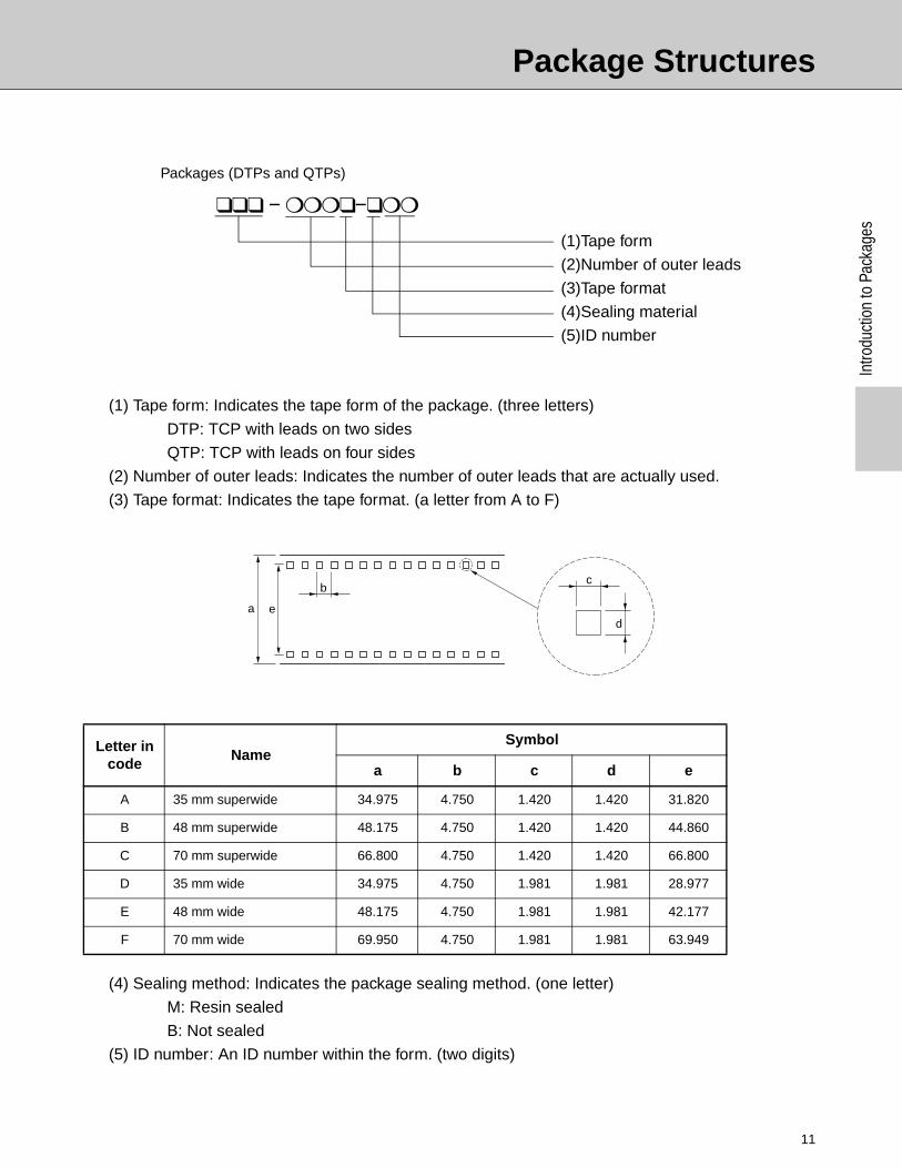
(1) Tape form: Indicates the tape form of the package. (three letters)
DTP: TCP with leads on two sides
QTP: TCP with leads on four sides
(2) Number of outer leads: Indicates the number of outer leads that are actually used.
(3) Tape format: Indicates the tape format. (a letter from A to F)
(4) Sealing method: Indicates the package sealing method. (one letter)
M: Resin sealed
B: Not sealed
(5) ID number: An ID number within the form. (two digits)
Letter in code
NameSymbol
a b c d e
A 35 mm superwide 34.975 4.750 1.420 1.420 31.820
B 48 mm superwide 48.175 4.750 1.420 1.420 44.860
C 70 mm superwide 66.800 4.750 1.420 1.420 66.800
D 35 mm wide 34.975 4.750 1.981 1.981 28.977
E 48 mm wide 48.175 4.750 1.981 1.981 42.177
F 70 mm wide 69.950 4.750 1.981 1.981 63.949
Packages (DTPs and QTPs)
❑❑❑ − ❍❍❍❑−❑❍❍
(1)Tape form
(2)Number of outer leads
(3)Tape format
(4)Sealing material
(5)ID number
a e
bc
d
Package Structures
12
1.7 Marking
Marking includes Fujitsu’s standard marking and customer-specified marking. Section 1.7.1 showsthe format for standard marking; if customer-specified marking is desired, the customer shouldestablish the marking specifications while observing the restrictions shown in section 1.7.2 Notethat in the case of customer-specified marking, the Engineering Samples (ES) will bear thestandard marking, and the Commercial Samples (CS) will bear the customer-specified marking.
If a format other than those shown in this data book is desired, consult with the Fujitsu sales officebeforehand.
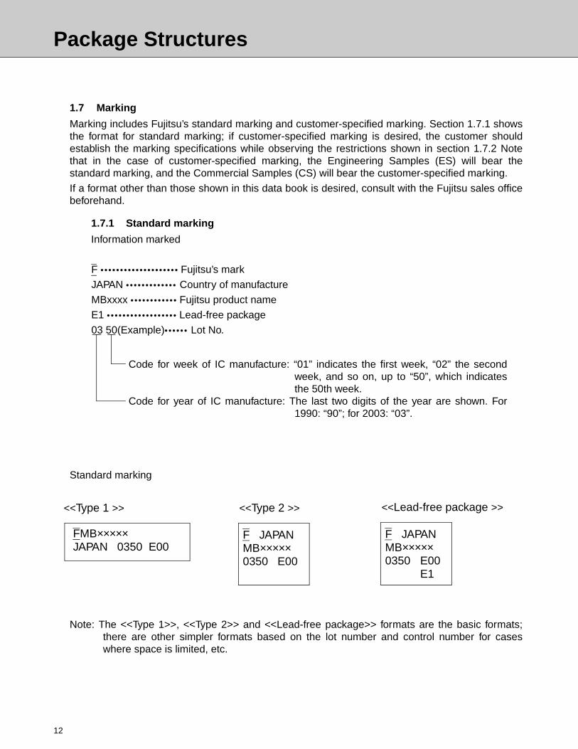
1.7.1 Standard marking
Information marked
Standard marking
Note: The <<Type 1>>, <<Type 2>> and <<Lead-free package>> formats are the basic formats;there are other simpler formats based on the lot number and control number for caseswhere space is limited, etc.
F •••••••••••••••••••• Fujitsu’s mark
JAPAN ••••••••••••• Country of manufacture
MBxxxx •••••••••••• Fujitsu product name
E1 •••••••••••••••••• Lead-free package
03 50(Example)•••••• Lot No.
Code for week of IC manufacture: “01” indicates the first week, “02” the secondweek, and so on, up to “50”, which indicatesthe 50th week.
Code for year of IC manufacture: The last two digits of the year are shown. For1990: “90”; for 2003: “03”.
<<Type 1 >> <<Type 2 >>
FMB×××××JAPAN 0350 E00
F JAPANMB×××××0350 E00
<<Lead-free package >>
F JAPANMB×××××0350 E00
E1
Package Structures
11
Intro
duct
ion
to P
acka
ges
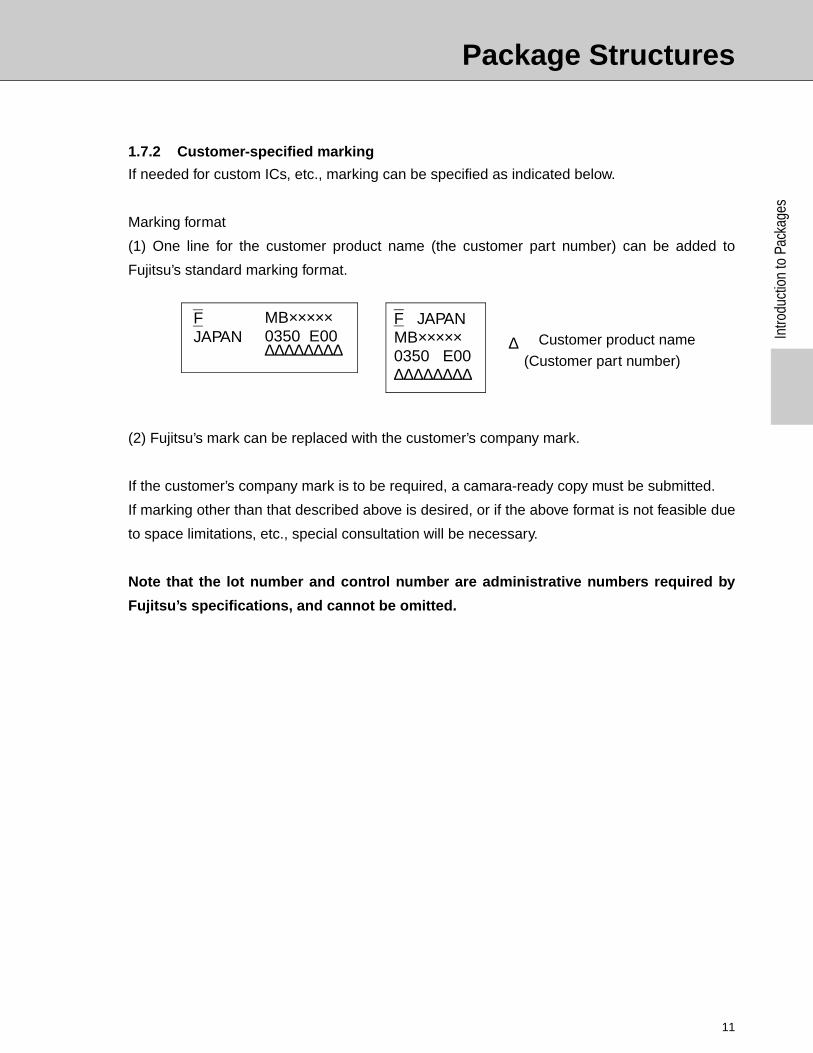
1.7.2 Customer-specified marking
If needed for custom ICs, etc., marking can be specified as indicated below.
Marking format
(1) One line for the customer product name (the customer part number) can be added to
Fujitsu’s standard marking format.
(2) Fujitsu’s mark can be replaced with the customer’s company mark.
If the customer’s company mark is to be required, a camara-ready copy must be submitted.
If marking other than that described above is desired, or if the above format is not feasible due
to space limitations, etc., special consultation will be necessary.
Note that the lot number and control number are administrative numbers required by
Fujitsu’s specifications, and cannot be omitted.
FJAPAN
F JAPANMB×××××0350 E00∆∆∆∆∆∆∆∆
Customer product name
(Customer part number)
MB×××××0350 E00∆∆∆∆∆∆∆∆ ∆
Package Structures
12
1.8 Future Trends in Packages
1.8.1 Diversification
Semiconductor packages can be broadly classified into two types: pin inserted types andsurface mounted types. The main package format has changed from DIP to types such asSOP, QFP, and PGA. In addition, a package is now expected to provide the following features:
• High-density mounting in order to permit lighter and smaller designs as more equipmentbecomes portable
• Multiple I/O pins, required as devices are integrated on larger scales and more functionsare offered
• Faster speed
• Lower cost
Given the balance between mounting technology and the design standards for the referenceprinted circuit board that serves as the mounting platform, progress in the area of surfacemounting and leadless packages (except for vertical packages) should be attainable.
Development is already progressing on representative types such as BGAs and CSPs. Thefeatures of each of these types and their future direction of development are described below:
• SOPs are mainly suited for packages with up to 100 pins. There are versions in whichthe pitch is even smaller or the package profile is even lower, such as TSOPs andUTSOPs, and the trend is towards CSPs. One variation is the SVP, as progress inutilizing all three dimensions is made in order to permit high-density mounting ofmemory.
• QFP normally have from 50 to 300 pins.Packages for an even smaller pitch are inprogress and being deployed into QTPs and TPQFPs using tape carriers.
• PGAs are a package type suited for ICs with a large number of pins (200 to 500 pins).SPGAs offer an even narrow pitch, and BGAs are being developed for the future.
1.8.2 Future formats
In the future, due to the demand for high-density mounting, surface mounted packages willgrow in number, while the demand for higher speeds will drive the growth of leadlesspackages.
Cost requirements will cause growth in plastic packages, while the characteristics of ceramicpackages will make them required for applications that demand high reliability, for devices thatoperate at high speeds and consume a lot of power, and for large chips.
With these trends in mind, Fujitsu’s own package development efforts will continue toemphasize mounting efficiency while paying attention to the need for compatibility with theJEDEC*1 standards, the JEITA*2 standards, and packages from other manufacturers.
*1:Joint Electron Device Engineering Council
*2:Japan Electronics & Information Technology Industries Association
Package Structures
11
Intro
duct
ion
to P
acka
ges
1.8.3 Custom packages
In addition to the increasingly important diversity of product types, there is also a growing trendtowards diversity among semiconductor types and mounting methods. As a manufacturer ofASICs, it is important for Fujitsu to be able to quickly grasp market trends and make strategiccontributions to customer product differentiation efforts.
At Fujitsu, in addition to promoting new standard packages in order to meet market demand forsmaller and thinner packages, through joint development of CSPs and BGAs, we are alsostriving to supply "user-friendly" custom packages that satisfy the needs of a single customer.We make every effort to meet with customers and discuss in detail their desires concerning theform of the package, the dimensions, the number of leads, the exterior processing, etc., andthen we strive to meet those needs quickly and flexibly.
1.8.4 System-In-Package
Recently, with the evolution of the digital consumer application, added value of the packageshas had the tendency to put emphasis on high quality compared to compact and lightweight.As mobile phones increase functional circuit points and necessary memory capacity, theydevelop from a simple tool for talking into mobile multimedia applications.
Also development is rapidly progressing on network associate devices including communica-tion applications and server. Quicker bus and interface technologies are attracting attention.Furthermore, it will be necessary to advance the development of multiple embedded chips andSiP which control the speed.
The problem in the future will be to find a way to divide the whole system into SoC and SiP atthe designing stage to offer the best quality, cost and mounting area. In short, SiP is requirednot only to be a low cost method using SoC but also to have the same quality as SoC. There-fore, we pay attention to the following technical factors:
(1)Unity of SoC/SiP design environment
(2)Fine pitch COC technology
(3)Rewiring technology
(4)DFT technology of Sip
And we aim to offer SiP which has a higher level.

MEMO
2.1 Overview ................................................................................................... 27
2.2 Mounting Methods
2.2.1 Lead inserted type .......................................................................... 28
2.2.2 Surface mounted type ..................................................................... 29
2.2.3 Precautions on mounting................................................................. 32
2.3 Surface Mounted Plastic Package Reliability
2.3.1 Features of surface mounted packages .......................................... 38
2.3.2 Mechanism behind degradation of humidity resistance
characteristics due to thermal stress during mounting .................... 39
2.3.3 Measures to improve humidity resistance characteristics ............... 41
2.3.4 Mounting Rank and Recommended Mounting Conditions .............. 41
2.3.5 Storage and drying processing........................................................ 48
2.3.6 Reliability data ................................................................................. 48
2.4 Storage ...................................................................................................... 59
Package Mounting Methods2

Overview
27
Pack
age
Mou
ntin
g M
etho
ds
2.1 Overview
There are two basic methods for mounting packages. One is the flow soldering method, and theother is the reflow soldering method.
The flow soldering method, which is widely used for lead inserted type packages, uses a jet-typesolder bath to mount packages on printed circuit boards.
As electronic devices become smaller and lighter, IC packages are also expected to becomesmaller and thinner. As a result, in recent years there has been rapid growth in surface mountedpackages, and surface mounting technology based on the reflow soldering method has garneredmuch attention.
One point that is important is that the flow soldering method used with lead insertion packagesdoes not subject the package to much thermal stress, while in the reflow soldering method usedwith surface mounted packages, the package as a whole is heated, so that there is a great deal ofthermal stress placed on the package, which must be noted during mounting.
This chapter will provide an overview of the mounting methods, the level of package moistureabsorption, and the proper handling of packages, all in order to permit surface mounted packagesto be mounted in a proper manner that preserves their reliability.
Mounting Methods
28
2.2 Mounting Methods
2.2.1 Lead inserted type
There are two methods for mounting lead inserted type packages on a printed circuit board:one method where the solder is applied directly to the printed circuit board, and anothermethod where the package is mounted in a socket on the board.
When applying solder directly to the board, the leads are inserted into the mounting holes inthe printed circuit board first, and the flow soldering method (wave soldering method) is usedwith jet solder. This is the most popular and widely used method for mounting packages on aprinted circuit board.
However, during the soldering process, heat in excess of the normal maximum rating for thestorage temperature is applied to the leads. As a result, quality assurance concerning heatresistance during soldering limits the soldering process to the levels shown below; do notexceed these levels during soldering work.
1) Solder temperature and immersion time
260 °C (500 °F), 10 seconds or less
2) Lead immersion position
Up to a distance of at least 1 to 1.5 mm from the main body of the package
3) When mounting an element using the solder flow method, ensure that the elementitself is not immersed in the solder.
4) When using flux, avoid chlorine based fluxes; instead, use a resin-based flux.
Note, however, that if the module leads are exposed to the solder for a long period of time, sol-der on the module board may melt and previously mounted ICs may become detached.
Also be careful to prevent any solder from coming into direct contact with the packagesmounted on the module.
When using socket mounting, in some cases when the surface treatment of the socket pins isdifferent from the surface metal of the IC leads, problems due to poor contact may arise.
Therefore, a check of the surface treatment of the socket contacts and of the surface treatmentof the IC leads is recommended.
Mounting Methods
29
Pack
age
Mou
ntin
g M
etho
ds
2.2.2 Surface mounted type
Compared to the lead inserted type, surface mounted packages have finer, thinner leads,which means that the leads are more easily bent. In addition, as packages come to have moreand more pins, the lead pitch is becoming narrower, making handling more difficult.
When the pitch of an IC is narrow, problems such as open pins caused by bent leads or shortcircuits caused by solder bridges occur easily; therefore, suitable mounting technologybecomes a necessity.
Surface mounted packages include flat packages with gull-wing leads or straight leads, pack-ages with J-leaded, and ball-grid array packages(BGA); the packages can be either plastic orceramic. In the case of surface mounted packages, the solder reflow method is recommendedas the mounting method for either type of package.
Fig. 1 illustrates the basic process for mounting.
Fig. 1 Flow Chart of Basic Mounting Process
There are a variety of methods for soldering surface mounted packages onto a printed circuitboard. Some of these methods are described below.
The mounting methods can be broadly classified into two types: partial heating methods andthe total heating methods. The partial heating methods are desirable from a reliability stand-point since the thermal stress is small, but from the standpoint of mass production such meth-ods are somewhat more difficult to implement.
Boards(1) Solder paste application
Component(2) Component preprocessing (baking,preliminary soldering)
(3) Component placement
(4) Solder reflow
(5) Cleaning/drying
Visual check/testing
Mounting Methods
30
(1)Partial heating methods
Soldering method Advantages Disadvantages
Manual method • Less stress placed on IC package
• Bent leads can be repaired
• Low equipment/ facility cost
• Limited suitability for mass production
• Danger of electrostatic damage
Block heater method • Less stress placed on IC package
• Bent leads can be repaired
• No problem if the leads are raised a little
• Faster than the manual method
• Limited suitability for mass production
• Danger of electrostatic damage
Laser method • Less stress placed on IC package
• Limited suitability for mass production
• Problems arise if leads are raised slightly
Hot air method • Less stress placed on IC package
• Low operating costs
• Very low suitability for mass production
Soldering iron
Pulse current
Heater
Laser
Hot air
Mounting Methods
31
Pack
age
Mou
ntin
g M
etho
ds
(2)Total heating methods
Soldering method Advantages Disadvantages
Full dip method• Highly suited
for mass pro-duction
• Existing tech-niques and facilities can be used
• Low operating costs
• Places the most stress on package
Infrared reflow method • Highly suited for mass pro-duction
• Low operating costs
• Places comparatively large amount of stress on package
Vapor phase reflow method
• Highly suited for mass pro-duction
• Places compar-atively little stress on pack-age
• Uniformity of temperature distribution is excellent
• Operating costs are high
Hot air heating method (used with far infrared heat) • Places compar-atively little stress on pack-age
• Highly suited for mass pro-duction
• Oxidation due to sur-rounding air may occur
Underside heating method • High tempera-tures are not applied directly to the package
• Cannot be used with double-sided boards
Melted solder
Infrared heater
Saturated steam
Inert liquid(florinate)
Heater
Far infrared heater
Forced convection
Conveyor belt
Heater
Mounting Methods
32
2.2.3 Precautions on mounting
Points of consideration concerning mounting work are explained below.
(1) Boards
Packages can be mounted on a variety of boards, including resin boards made of materialssuch as paper phenol or glass epoxy, ceramic boards, and flexible printed circuit boards, andwhen selecting the board material it is essential to give due consideration to factors such asmatching the thermal expansion coefficients of the components to be mounted, electrical andmechanical characteristics, heat dissipation characteristics, the total reliability level, and cost.In addition, the reliability and production yield in terms of the wiring pattern on the componentmounting surface also become important factors.
Figs. 2 and 3 show examples of design for surface patterns. In the design stage, considerationshould be given to ease of mounting, reliability of the connections, pattern spacing, and thepossibility of solder bridge formation.
Fig. 2 Example of Surface Pattern Design Criteria for SOPs and QFPs
P
L
W
QFP
w
L
0.40mm 0.20mm
20.25mm
(Typ value) + 0.60mm Also applicable to SOP.
For package with a pitch of 0.5 mm or less;w (Typ value) + 0.03 mm ≤ W ≤ P × 0.6 mm
For others;w (Typ value) ≤ W ≤ P − 0.30 mm
Mounting Methods
33
Pack
age
Mou
ntin
g M
etho
ds
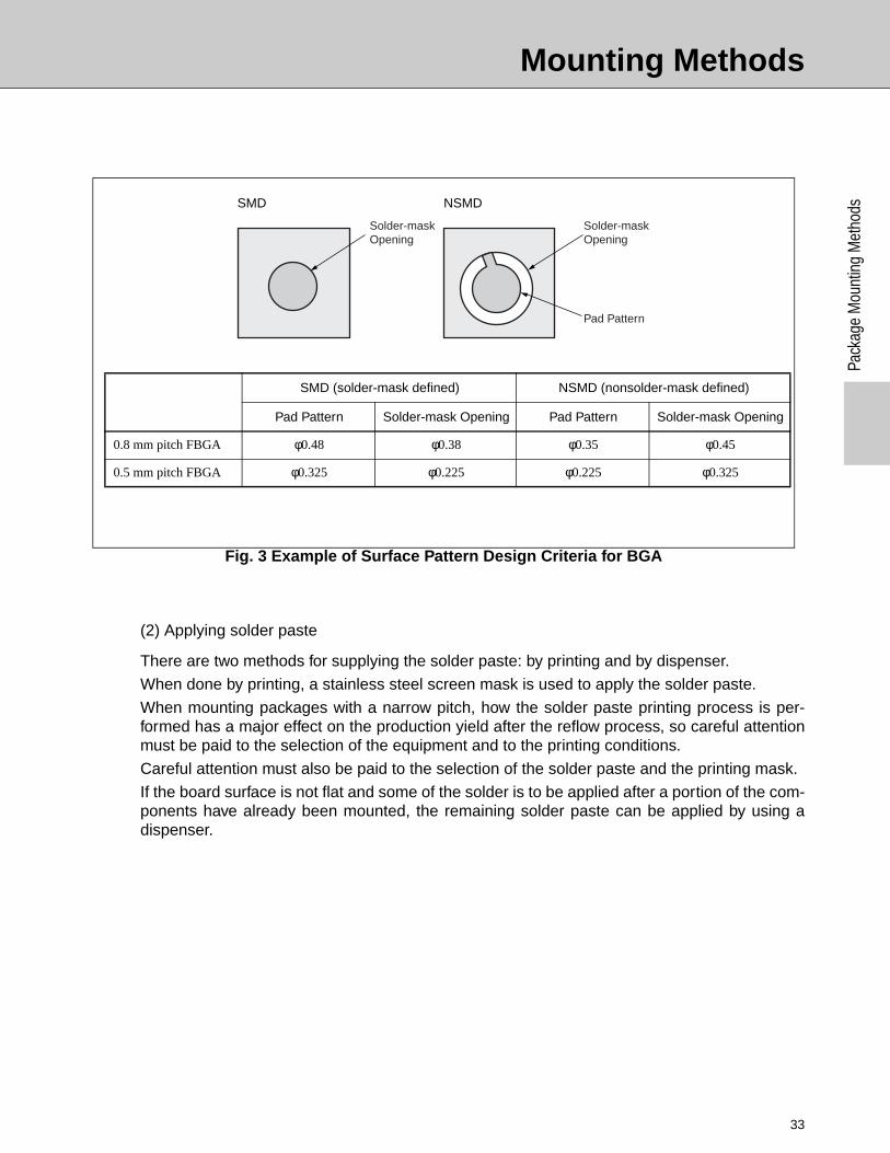
Fig. 3 Example of Surface Pattern Design Criteria for BGA
(2) Applying solder paste
There are two methods for supplying the solder paste: by printing and by dispenser.
When done by printing, a stainless steel screen mask is used to apply the solder paste.
When mounting packages with a narrow pitch, how the solder paste printing process is per-formed has a major effect on the production yield after the reflow process, so careful attentionmust be paid to the selection of the equipment and to the printing conditions.
Careful attention must also be paid to the selection of the solder paste and the printing mask.
If the board surface is not flat and some of the solder is to be applied after a portion of the com-ponents have already been mounted, the remaining solder paste can be applied by using adispenser.
Solder-maskOpening
Solder-maskOpening
Pad Pattern
SMD NSMD
SMD (solder-mask defined) NSMD (nonsolder-mask defined)
Pad Pattern Solder-mask Opening Pad Pattern Solder-mask Opening
0.8 mm pitch FBGA φ0.48 φ0.38 φ0.35 φ0.45
0.5 mm pitch FBGA φ0.325 φ0.225 φ0.225 φ0.325
Mounting Methods
34
(3) Solder paste
The solder paste is a mixture of solder powder (normally #250 to 325) mixed with flux.
The merits of using solder paste include:• It is easy to control the amount of solder used.
• It is possible to use the viscosity of the paste to temporarily hold components in place.
• There are no impurities from a solder bath, etc.
• It is well suited for automation and mass production.
The most common type of solder is lead-tin eutectic type, but when soldering boards or com-ponents that use silver-lead for conductors, a eutectic type solder with a silver content of about2% or 3% is used.
The fluxes used in the paste include fluxes that require cleaning and fluxes that do not requirecleaning. If using a cleaning-type flux, you need to determine the correct cleaning procedure.
Key points to consider in the selection of flux include:
a)Selection based on catalog values• Size and shape of the solder powder
• Solder composition
• Amount of flux and chlorine included
b)Evaluation criteria for actual trials• Good patterning characteristics (deposits well)
• No change in the viscosity and uniformity of the mixture of solder powder and flux over
time
• Continuous printing possible
• Very little dripping or formation of solder balls when melted
• Easy to clean, with little flux residue, no-discoloration or staining
Although the cost of the solder paste is also important, the total manufacturing cost in terms ofproduction yield, etc., must be taken into consideration when selecting a paste, not just thecost of the paste itself.
Before beginning mass production, a thorough study should be conducted and then thosematerials that best fit the conditions under which they will be used should be selected.
Solder paste is normally applied through a printing process, using a screen mask about 150µm thick.
Mounting Methods
35
Pack
age
Mou
ntin
g M
etho
ds
(4) Component preprocessing (Baking surface mounted plastic packages)
Unlike ceramic packages, plastic packages absorb moisture when exposed to atmosphere.Although this does not present a reliability problem during storage, if a plastic package that hasabsorbed moisture is soldered by the reflow method, the package may crack. Although itdepends on the package type and the reflow method, it is important to note that some pack-ages must undergo a baking process before the reflow process. (For details, refer to section2.3, “Surface Mounted Plastic Package Reliability.”)
(5) Component placement
Equipment that positions surface mounted package components is available from a variety ofmanufacturers in worldwide. When selecting such equipment, it is necessary to consider thenumber of components it will handle and the manner in which the components are packaged(in containers, trays, or on tape).
Because the leads on flat packages extend outwards, they are easily bent. Because repair isdifficult once the leads are bent, great care must be taken when handling the packages.
As the electrode part of BGA package pins is made from soft metal such as solder, care isrequired to ensure that the pin electrodes are not contaminated by scratches or dirt that canaffect mounting.
(6) Full solder dip (wave soldering method)
When using the full solder dip method for mounting, observe the following conditions.
(Contact a Fujitsu sales representative for details on those packages and products for whichfull solder dipping is available.)
Solder bath temperature: 260°C max. (500°F max.)
Time: Less than 5 seconds
(7) Solder reflow
The typical reflow methods are: a) hot air reflow; b) infrared reflow; and c) vapor phase reflow.General descriptions of each of these methods are provided below. Note that the use of fullsolder dipping should be avoided.
a)Hot air reflow
This reflow method uses convective thermal propagation with heat-saturated air.
There are two different types of methods: the far infrared combination type and the hotair circulation type.
Advantages • Temperature profile can be controlled comparatively well.
• Temperature distribution can be made relatively uniform.
• Operating cost is low.
Disadvantages • Reflow in a normal oxidizing atmosphere.
• Processing capability decreases somewhat.
Mounting Methods
36
b) Infrared reflow
This reflow method uses radiant heat from an infrared heater.
Advantages • Processing capability is high.
• Temperature profile can be controlled comparatively well.
• Operating cost is low.
Disadvantages • Temperature differences can arise due to differences in radiationabsorption rates on the board.
• Caution is required, since the flux is easily blackened.
• Reflow in a normal oxidizing atmosphere.
c) Vapor phase reflow
This reflow method uses the latent heat of vaporization of an inert liquid.
Advantages • Uniform temperature distribution.
• Reflow in an inert atmosphere.
• No fear of overheating. (Heat is not applied above the boiling point ofthe inert liquid.)
Disadvantages • Temperature profile is limited.
• Operating cost is high.
• Processing capability decreases somewhat.
• Attention must be paid to ventilation.
• Equipment is expensive.
(8) Manual soldering (partial heating method)
This method uses a soldering iron; soldering is done with the IC fixed in place by flux or adhe-sive.
Conditions: Temperature: 350 °C MAX (662°F max.)Time: 3 seconds max./pin
(9) Cleaning
After soldering, clean away any flux residue.
If any flux left on the printed circuit board begins to absorb moisture, it can have a negativeimpact on reliability due to degradation of the insulation resistance or corrosion of the leadsdue to the chlorine component of the flux; therefore, cleaning is recommended. Refer to Table2 for details on the cleaning requirements.
The following cautions should be observed during cleaning:
a) Do not touch printed surfaces until the cleaning fluid dries.
b) When solder paste was used for mounting, solder balls may have formed, depending onthe paste type, paste quality, mounting conditions, etc.; therefore, pay attention to theneed to clean away any solder ball residue as well.
Mounting Methods
37
Pack
age
Mou
ntin
g M
etho
ds
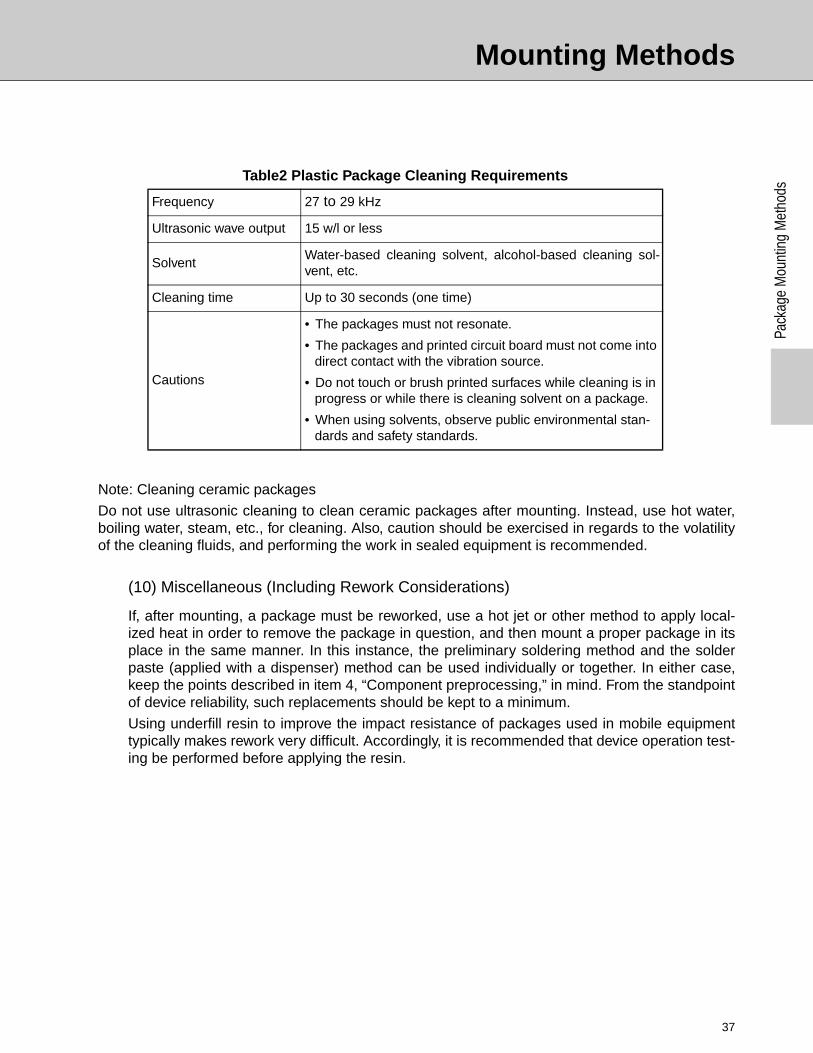
Table2 Plastic Package Cleaning Requirements
Note: Cleaning ceramic packages
Do not use ultrasonic cleaning to clean ceramic packages after mounting. Instead, use hot water,boiling water, steam, etc., for cleaning. Also, caution should be exercised in regards to the volatilityof the cleaning fluids, and performing the work in sealed equipment is recommended.
(10) Miscellaneous (Including Rework Considerations)
If, after mounting, a package must be reworked, use a hot jet or other method to apply local-ized heat in order to remove the package in question, and then mount a proper package in itsplace in the same manner. In this instance, the preliminary soldering method and the solderpaste (applied with a dispenser) method can be used individually or together. In either case,keep the points described in item 4, “Component preprocessing,” in mind. From the standpointof device reliability, such replacements should be kept to a minimum.
Using underfill resin to improve the impact resistance of packages used in mobile equipmenttypically makes rework very difficult. Accordingly, it is recommended that device operation test-ing be performed before applying the resin.
Frequency 27 to 29 kHz
Ultrasonic wave output 15 w/l or less
SolventWater-based cleaning solvent, alcohol-based cleaning sol-vent, etc.
Cleaning time Up to 30 seconds (one time)
Cautions
• The packages must not resonate.
• The packages and printed circuit board must not come into direct contact with the vibration source.
• Do not touch or brush printed surfaces while cleaning is in progress or while there is cleaning solvent on a package.
• When using solvents, observe public environmental stan-dards and safety standards.
Surface Mounted Plastic Package Reliability
38
2.3 Surface Mounted Plastic Package Reliability
The heat stress that surface mounted plastic packages are subjected to when they are mountedadversely affects their humidity resistance characteristics. This section describes the humidityresistance characteristics of surface mounted plastic packages.
2.3.1 Features of surface mounted packages
Compared with lead inserted types, surface mounted packages offer the following advantagesand disadvantages.(1) Advantages
• Higher mounting densities are possible, making thinner and lighter devices possible.
• Packages can have more pins.
• Surface mounted packages offer benefits from the standpoint of electrical characteris-
tics.
• Because through holes are not needed, costs are lower.
• Surface mounted packages are suited for automated assembly lines.
(2) Disadvantages
• Surface mounted packages are vulnerable to thermal stress during mounting, which can
result in cracked packages or poor humidity resistance characteristics.
• Because the external leads are thin, they are easily bent.
• Because the pitch is very small, solder bridges form easily.
Surface Mounted Plastic Package Reliability
39
Pack
age
Mou
ntin
g M
etho
ds
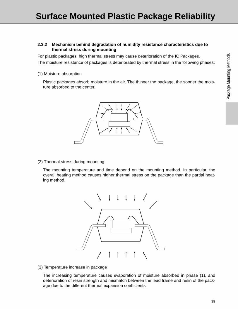
2.3.2 Mechanism behind degradation of humidity resistance characteristics due to thermal stress during mounting
For plastic packages, high thermal stress may cause deterioration of the IC Packages.
The moisture resistance of packages is deteriorated by thermal stress in the following phases:
(1) Moisture absorption
Plastic packages absorb moisture in the air. The thinner the package, the sooner the mois-ture absorbed to the center.
(2) Thermal stress during mounting
The mounting temperature and time depend on the mounting method. In particular, theoverall heating method causes higher thermal stress on the package than the partial heat-ing method.
(3) Temperature increase in package
The increasing temperature causes evaporation of moisture absorbed in phase (1), anddeterioration of resin strength and mismatch between the lead frame and resin of the pack-age due to the different thermal expansion coefficients.
Surface Mounted Plastic Package Reliability
40
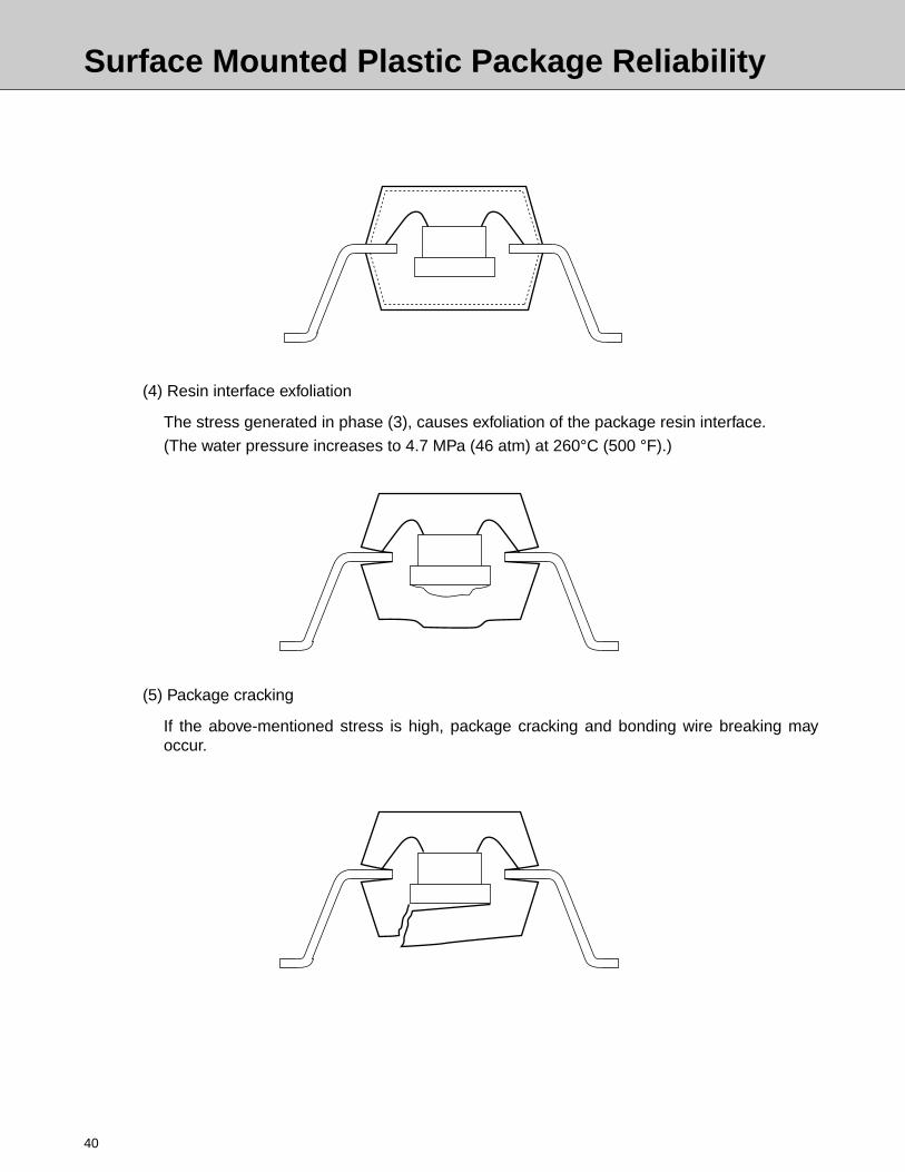
(4) Resin interface exfoliation
The stress generated in phase (3), causes exfoliation of the package resin interface.
(The water pressure increases to 4.7 MPa (46 atm) at 260°C (500 °F).)
(5) Package cracking
If the above-mentioned stress is high, package cracking and bonding wire breaking mayoccur.
Surface Mounted Plastic Package Reliability
41
Pack
age
Mou
ntin
g M
etho
ds
2.3.3 Measures to improve humidity resistance characteristics
In response to the mechanisms described above that contribute to the degradation of a pack-age’s humidity resistance characteristics, Fujitsu is taking the following measures in order toimprove reliability.
(1) Improvement of mold resins
Fujitsu is striving to improve the sealing power of resins, reduce the stress that they aresubjected to, and to increase their purity.
(2) Improvement of the lead frame
It is essential to eliminate the boundary surface separations that form due to thermal expan-sion of the lead frame and the resin when thermal stress is applied during the mounting pro-cess.
(3) Improvement of packaging materials for shipment
Since one of the mechanisms described was the absorption of moisture by plastic ICswhich in turn lead to a degradation of humidity resistance characteristics, Fujitsu packagesICs in an aluminum-laminate pouch that is highly impermeable to moisture, and with silicagel placed inside the pouch.
2.3.4 Mounting Rank and Recommended Mounting Conditions
Surface mounted plastic packages occur in many package sizes and thicknesses, and a vari-ety of resistances to thermal stress during mounting. For this reason Fujitsu establishes anallowable number of days from unpackaging to mounting for each product. This is called theproduct’s mounting rank, and it differs according to package type and mounting conditions.Table 3 shows the types of mounting ranks and corresponding recommended mounting condi-tions.
Even within the same package, the mounting rank may vary between products so that usersare advised to specifically confirm mounting ranks by contacting a Fujitsu marketing represen-tative.
Surface Mounted Plastic Package Reliability
42
Table3. Mounting Rank Types and Recommended Mounting Conditions
Fujitsu mounting ranks are indicated in the format: Rnn Smm Jkk Hxx, or Rnn Smm Jkk Mxx.
These formats have the following meaning:
Rnn: Acceptable reflow mounting conditions in terms of the mounting method and temperatureprofile shown in Fig.4-1.
Smm: Acceptable mounting conditions for wave soldering (260 °C max, 5 seconds or less)
Symbol Acceptable mounting conditions
RZ02 × reflow, no control required for moistureabsorption
RY0 2 × reflow, within 1 year
R28 2 × reflow, within 28 days
R14 2 × reflow, within 14 days
R08 2 × reflow, within 8 days
R04 2 × reflow, within 4 days
R02 2 × reflow, within 2 days
R00 Not acceptable for 2 × reflow
Xnn Limited to 1 × reflow, within nn days
Symbol Acceptable mounting conditions
SZ01 × solder dip, no control required for moisture absorption
SY0 1 × solder dip, within 1 year
S28 1 × solder dip, within 28 days
S14 1 × solder dip, within 14 days
S08 1 × solder dip, within 8 days
S04 1 × solder dip, within 4 days
S02 1 × solder dip, within 2 days
S00 Not acceptable for 1 × solder dip
SPn 1 × solder dip, bake after unpackaging, within n days
Surface Mounted Plastic Package Reliability
43
Pack
age
Mou
ntin
g M
etho
ds
Jnn: JEDEC moisture sensitivity level, according to IPC/JEDEC J-STD-020A.
Hnn: Acceptable reflow mounting conditions in terms of the mounting method and temperatureprofile shown in Fig.4-2.
Symbol JEDEC moisture sensitivity level
J01 1
J02 2
J2a 2a
J03 3
J04 4
J05 5
J5a 5a
J06 6
J00Not applicable to JEDECstandard
Symbol Acceptable mounting conditions
HZ02 × reflow, no control required for moisture absorption
HY0 2 × reflow, within 1 year
H28 2 × reflow, within 28 days
H14 2 × reflow, within 14 days
H08 2 × reflow, within 8 days
H04 2 × reflow, within 4 days
H02 2 × reflow, within 2 days
Surface Mounted Plastic Package Reliability
44
Mnn: Acceptable reflow mounting conditions in terms of the mounting method and temperature
profile shown in Fig.4-3.
• Mounting by partial heating methods:
Partial heating methods may be used with any mounting rank.
Symbol Acceptable mounting conditions
MZ02 × reflow, no control required for moisture absorption
MY0 2 × reflow, within 1 year
M28 2 × reflow, within 28 days
M14 2 × reflow, within 14 days
M08 2 × reflow, within 8 days
M04 2 × reflow, within 4 days
M02 2 × reflow, within 2 days
Surface Mounted Plastic Package Reliability
45
Pack
age
Mou
ntin
g M
etho
ds
Fig.4-1 Temperature profile for hot air reflow/infrared reflow scheme 1
(a)Temperature increase gradient Average: 1 °C/s to 4 °C/s (33.8°F/s to 39.2°F /s)
(b)Preliminary heating Temperature: 150 °C to 190 °C (302°F to 374°F), 60 s to 120 s
(c)Temperature increase gradient Average: 1 °C/s to 4 °C/s (33.8°F/s to 39.2°F /s)
(d)Actual heating Temperature: 240 °C(464°F) MAX.,235 °C (455°F) or more, 10 s or less(Temperature of the top of the package body)
(d’) Temperature: 210 °C(410°F) or more, 40 s or less
(e)Natural cooling or forced cooling
240 °C
210 °C
150 °C
RT
(a)
(c)(b) (e)
(d)
(d ’)
235 °C
Surface Mounted Plastic Package Reliability
46
Fig.4-2 Temperature profile for hot air reflow/infrared reflow scheme 2
(a)Temperature increase gradient Average: 1 °C/s to 4 °C/s (33.8°F/s to 39.2°F /s)
(b)Preliminary heating Temperature: 150 °C to 190 °C (302°F to 374°F), 60 s to 120 s
(c)Temperature increase gradient Average: 1 °C/s to 4 °C/s (33.8°F/s to 39.2°F /s)
(d)Actual heating Temperature: 260 °C(500°F) MAX.,255 °C (491°F) or more, 10 s or less(Temperature of the top of the package body)
(d’) Temperature: 220 °C(428°F) or more, 40 s or less
(e)Natural cooling or forced cooling
260 °C
210 °C
150 °C
RT
(a)
(c)(b) (e)
(d)
(d ’)
255 °C
Surface Mounted Plastic Package Reliability
47
Pack
age
Mou
ntin
g M
etho
ds
Fig.4-3 Temperature profile for hot air reflow/infrared reflow scheme 3
(a)Temperature increase gradient Average: 1 °C/s to 4 °C/s (33.8°F/s to 39.2°F /s)
(b)Preliminary heating Temperature: 150 to 190 °C (302°F to 374°F), 60 s to 120 s
(c)Temperature increase gradient Average: 1 °C/s to 4 °C/s (33.8°F/s to 39.2°F /s)
(d)Actual heating Temperature: 250 °C(482°F) MAX.,245 °C (473°F) or more, 10 s or less(Temperature of the top of the package body)
(d’) Temperature: 220 °C(428°F) or more, 40 s or less
(e)Natural cooling or forced cooling
Fig.4-4 Temperature profile for vapor phase reflow scheme (Reference)
(a)Temperature increase gradient 1 °C/s to 8 °C/s (33.8°F/s to 46.4°F/s)(b)Temperature 200 °C(392°F) or more [Typ: 215 °C(419°F)] Time: 30 s to 60 s
The temperature profiles in Fig.4-2 and Fig.4-3 are subject to change without priornotification. Users are advised to contact the Fujitsu Marketing Department for confirmation.
250 °C
210 °C
150 °C
RT
(a)
(c)(b) (e)
(d)
(d ’)
245 °C
215 °C200 °C
RT
(a) (b)
Surface Mounted Plastic Package Reliability
48
2.3.5 Storage and drying processing
Surface mounted plastic packages should be stored while still packed in the materials that theywere shipped in from Fujitsu. If you have any questions, contact Fujitsu.
2.3.6 Reliability data
Because surface mounted plastic packages are mounted by total heating methods, they areeasily affected by thermal stress during the mounting process, with the result that packagessometimes crack or their humidity resistance characteristics are adversely affected.
In addition to normal reliability evaluations, Fujitsu subjects surface mounted plastic packagesto Temperature Cycling tests and PCT tests after preprocessing the packages for solder heatresistance, all in order to evaluate reliability versus the stresses encountered during the mount-ing process.
Tables 3 to 16 show examples of the results of these evaluations.
Table3 Reliability Testing Results (Plastic BCC-48 MB15G202) 1. Life tests
2. Environmental tests
*1: Pre-condition: Baking 125 °C(257°F), 24 h + Moisture Absorption 85 °C/85%RH(185°F/85%RH), 48 h + IR 245 °C(473°F) Max.
*2: AC operating conditions: Power supply voltage; 3.6 V, Operating frequency; 1MHz / 2MHz*3: PCT-Bias operating conditions: Power supply voltage; 3.6 V
Test item Test conditions Number of TestsTest duration
(h)Number of
Failure
High Temperature Storage 150 °C (302 °F) 25 1000 0
High Temperature Operation Life (AC operation) ∗2 100 °C (212 °F) 55∗1 1000 0
Temperature Humidity Bias(AC operation) ∗2
85 °C/85%RH(185 °F/85%RH)
25∗1 1000 0
Test item Test conditions Number of Tests Number of Failure
Temperature Cycling−65 °C to 150 °C(−85 °F to 302°F)(200 cycles)
55∗1 0
Thermal Shock0 °C to 100 °C(32 °F to 212 °F)(200 cycles)
25 0
PCT 121 °C(249.8°F), 2.03E5 Pa,168 h 55∗1 0
PCT-Bias ∗3 121 °C(249.8°F), 2.03E5 Pa, 96 h 25 0
Surface Mounted Plastic Package Reliability
49
Pack
age
Mou
ntin
g M
etho
ds
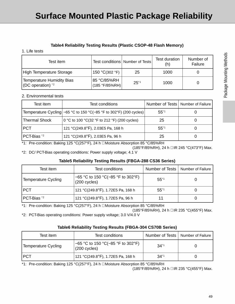
Table4 Reliability Testing Results (Plastic CSOP-48 Flash Memory) 1. Life tests
2. Environmental tests
*1: Pre-condition: Baking 125 °C(257°F), 24 h + Moisture Absorption 85 °C/85%RH(185°F/85%RH), 24 h + IR 245 °C(473°F) Max.
*2: DC/ PCT-Bias operating conditions: Power supply voltage; 4.1 V
Table5 Reliability Testing Results (FBGA-288 CS36 Series)
*1: Pre-condition: Baking 125 °C(257°F), 24 h + Moisture Absorption 85 °C/85%RH(185°F/85%RH), 24 h + IR 235 °C(455°F) Max.
*2: PCT-Bias operating conditions: Power supply voltage; 3.0 V/4.0 V
Table6 Reliability Testing Results (FBGA-304 CS70B Series)
*1: Pre-condition: Baking 125 °C(257°F), 24 h + Moisture Absorption 85 °C/85%RH(185°F/85%RH), 24 h + IR 235 °C(455°F) Max.
Test item Test conditions Number of TestsTest duration
(h)Number of
Failure
High Temperature Storage 150 °C(302 °F) 25 1000 0
Temperature Humidity Bias(DC operation) ∗2
85 °C/85%RH(185 °F/85%RH)
25∗1 1000 0
Test item Test conditions Number of Tests Number of Failure
Temperature Cycling −65 °C to 150 °C(−85 °F to 302°F) (200 cycles) 55∗1 0
Thermal Shock 0 °C to 100 °C(32 °F to 212 °F) (200 cycles) 25 0
PCT 121 °C(249.8°F), 2.03E5 Pa, 168 h 55∗1 0
PCT-Bias ∗2 121 °C(249.8°F), 2.03E5 Pa, 96 h 25 0
Test item Test conditions Number of Tests Number of Failure
Temperature Cycling−65 °C to 150 °C(−85 °F to 302°F)(200 cycles)
55∗1 0
PCT 121 °C(249.8°F), 1.72E5 Pa, 168 h 55∗1 0
PCT-Bias ∗2 121 °C(249.8°F), 1.72E5 Pa, 96 h 11 0
Test item Test conditions Number of Tests Number of Failure
Temperature Cycling−65 °C to 150 °C(−85 °F to 302°F)(200 cycles)
34∗1 0
PCT 121 °C(249.8°F), 1.72E5 Pa, 168 h 34∗1 0
Surface Mounted Plastic Package Reliability
50
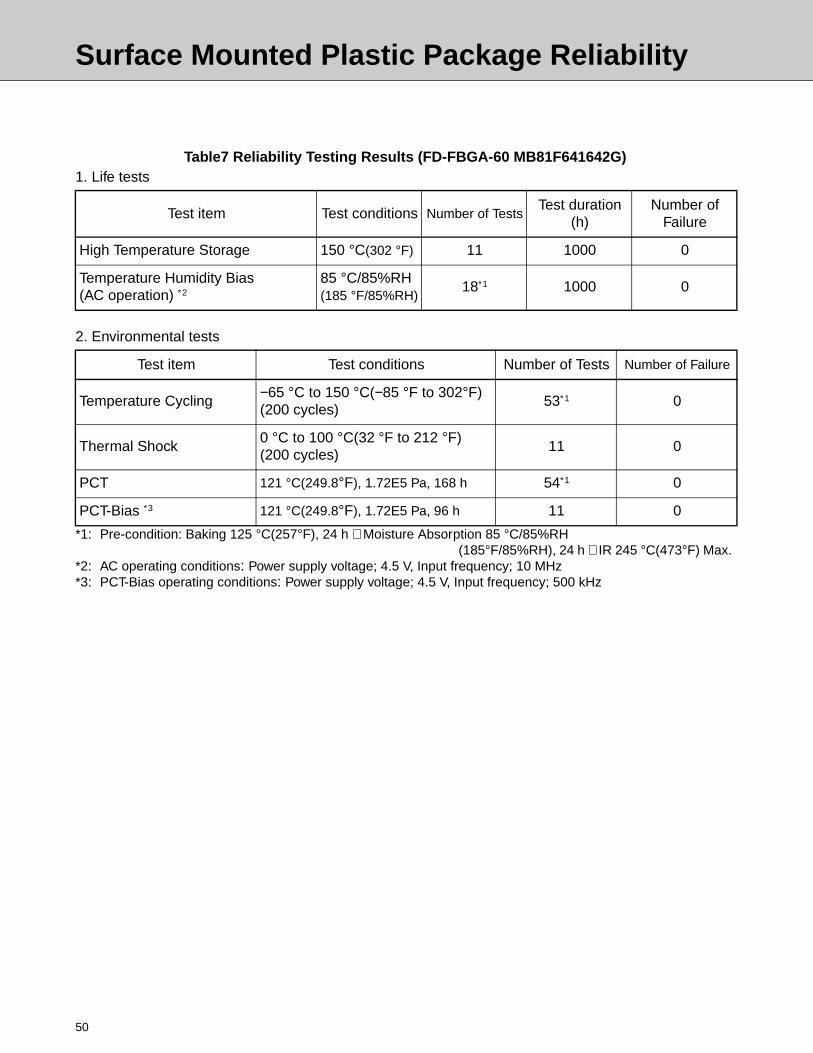
Table7 Reliability Testing Results (FD-FBGA-60 MB81F641642G) 1. Life tests
2. Environmental tests
*1: Pre-condition: Baking 125 °C(257°F), 24 h + Moisture Absorption 85 °C/85%RH(185°F/85%RH), 24 h + IR 245 °C(473°F) Max.
*2: AC operating conditions: Power supply voltage; 4.5 V, Input frequency; 10 MHz*3: PCT-Bias operating conditions: Power supply voltage; 4.5 V, Input frequency; 500 kHz
Test item Test conditions Number of TestsTest duration
(h)Number of
Failure
High Temperature Storage 150 °C(302 °F) 11 1000 0
Temperature Humidity Bias(AC operation) ∗2
85 °C/85%RH(185 °F/85%RH)
18∗1 1000 0
Test item Test conditions Number of Tests Number of Failure
Temperature Cycling−65 °C to 150 °C(−85 °F to 302°F)(200 cycles)
53∗1 0
Thermal Shock0 °C to 100 °C(32 °F to 212 °F)(200 cycles)
11 0
PCT 121 °C(249.8°F), 1.72E5 Pa, 168 h 54∗1 0
PCT-Bias ∗3 121 °C(249.8°F), 1.72E5 Pa, 96 h 11 0
Surface Mounted Plastic Package Reliability
51
Pack
age
Mou
ntin
g M
etho
ds
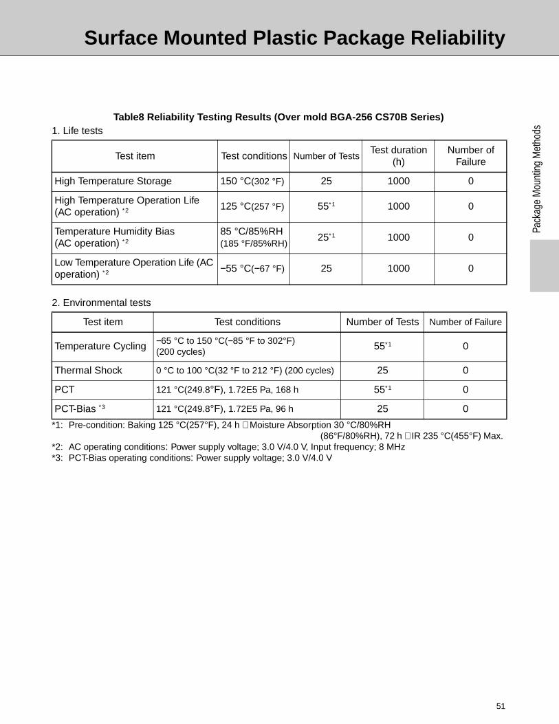
Table8 Reliability Testing Results (Over mold BGA-256 CS70B Series) 1. Life tests
2. Environmental tests
*1: Pre-condition: Baking 125 °C(257°F), 24 h + Moisture Absorption 30 °C/80%RH(86°F/80%RH), 72 h + IR 235 °C(455°F) Max.
*2: AC operating conditions: Power supply voltage; 3.0 V/4.0 V, Input frequency; 8 MHz*3: PCT-Bias operating conditions: Power supply voltage; 3.0 V/4.0 V
Test item Test conditions Number of TestsTest duration
(h)Number of
Failure
High Temperature Storage 150 °C(302 °F) 25 1000 0
High Temperature Operation Life (AC operation) ∗2 125 °C(257 °F) 55∗1 1000 0
Temperature Humidity Bias(AC operation) ∗2
85 °C/85%RH(185 °F/85%RH)
25∗1 1000 0
Low Temperature Operation Life (AC operation) ∗2 −55 °C(−67 °F) 25 1000 0
Test item Test conditions Number of Tests Number of Failure
Temperature Cycling −65 °C to 150 °C(−85 °F to 302°F)(200 cycles)
55∗1 0
Thermal Shock 0 °C to 100 °C(32 °F to 212 °F) (200 cycles) 25 0
PCT 121 °C(249.8°F), 1.72E5 Pa, 168 h 55∗1 0
PCT-Bias ∗3 121 °C(249.8°F), 1.72E5 Pa, 96 h 25 0
Surface Mounted Plastic Package Reliability
52
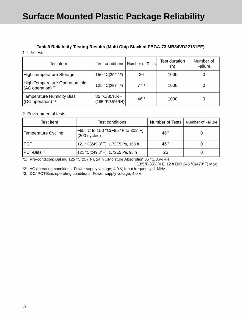
Table9 Reliability Testing Results (Multi Chip Stacked FBGA-73 MB84VD22181EE) 1. Life tests
2. Environmental tests
*1: Pre-condition: Baking 125 °C(257°F), 24 h + Moisture Absorption 85 °C/85%RH(185°F/85%RH), 12 h + IR 245 °C(473°F) Max.
*2: AC operating conditions: Power supply voltage; 4.0 V, Input frequency; 1 MHz*3: DC/ PCT-Bias operating conditions: Power supply voltage; 4.0 V
Test item Test conditions Number of TestsTest duration
(h)Number of
Failure
High Temperature Storage 150 °C(302 °F) 26 1000 0
High Temperature Operation Life (AC operation) ∗2 125 °C(257 °F) 77∗1 1000 0
Temperature Humidity Bias(DC operation) ∗3
85 °C/85%RH(185 °F/85%RH)
46∗1 1000 0
Test item Test conditions Number of Tests Number of Failure
Temperature Cycling−65 °C to 150 °C(−85 °F to 302°F)(200 cycles)
46∗1 0
PCT 121 °C(249.8°F), 1.72E5 Pa, 168 h 46∗1 0
PCT-Bias ∗3 121 °C(249.8°F), 1.72E5 Pa, 96 h 26 0
Surface Mounted Plastic Package Reliability
53
Pack
age
Mou
ntin
g M
etho
ds
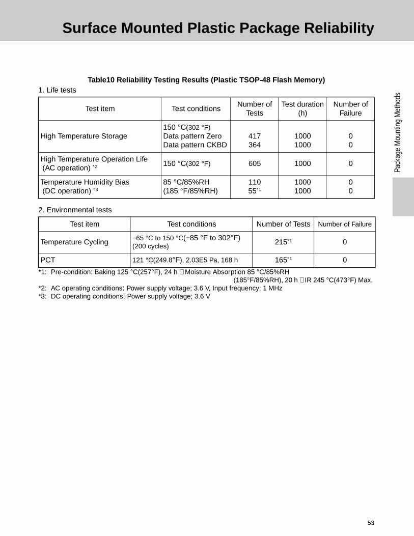
Table10 Reliability Testing Results (Plastic TSOP-48 Flash Memory) 1. Life tests
2. Environmental tests
*1: Pre-condition: Baking 125 °C(257°F), 24 h + Moisture Absorption 85 °C/85%RH(185°F/85%RH), 20 h + IR 245 °C(473°F) Max.
*2: AC operating conditions: Power supply voltage; 3.6 V, Input frequency; 1 MHz*3: DC operating conditions: Power supply voltage; 3.6 V
Test item Test conditionsNumber of
TestsTest duration
(h)Number of
Failure
High Temperature Storage150 °C(302 °F)Data pattern ZeroData pattern CKBD
417364
10001000
00
High Temperature Operation Life (AC operation) ∗2 150 °C(302 °F) 605 1000 0
Temperature Humidity Bias (DC operation) ∗3
85 °C/85%RH(185 °F/85%RH)
11055∗1
10001000
00
Test item Test conditions Number of Tests Number of Failure
Temperature Cycling −65 °C to 150 °C(−85 °F to 302°F)(200 cycles)
215∗1 0
PCT 121 °C(249.8°F), 2.03E5 Pa, 168 h 165∗1 0
Surface Mounted Plastic Package Reliability
54
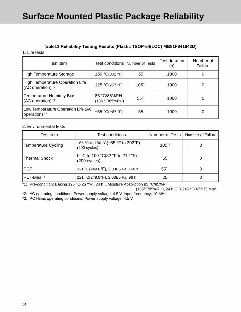
Table11 Reliability Testing Results (Plastic TSOP-54(LOC) MB81F641642D) 1. Life tests
2. Environmental tests
*1: Pre-condition: Baking 125 °C(257°F), 24 h + Moisture Absorption 85 °C/85%RH(185°F/85%RH), 24 h + IR 245 °C(473°F) Max.
*2: AC operating conditions: Power supply voltage; 4.5 V, Input frequency; 10 MHz*3: PCT-Bias operating conditions: Power supply voltage; 4.5 V
Test item Test conditions Number of TestsTest duration
(h)Number of
Failure
High Temperature Storage 150 °C(302 °F) 55 1000 0
High Temperature Operation Life (AC operation) ∗2 125 °C(257 °F) 105∗1 1000 0
Temperature Humidity Bias(AC operation) ∗2
85 °C/85%RH(185 °F/85%RH)
55∗1 1000 0
Low Temperature Operation Life (AC operation) ∗2 −55 °C(−67 °F) 55 1000 0
Test item Test conditions Number of Tests Number of Failure
Temperature Cycling −65 °C to 150 °C(−85 °F to 302°F)(200 cycles)
105∗1 0
Thermal Shock0 °C to 100 °C(32 °F to 212 °F)(200 cycles)
55 0
PCT 121 °C(249.8°F), 2.03E5 Pa, 168 h 55∗1 0
PCT-Bias ∗3 121 °C(249.8°F), 2.03E5 Pa, 96 h 25 0
Surface Mounted Plastic Package Reliability
55
Pack
age
Mou
ntin
g M
etho
ds
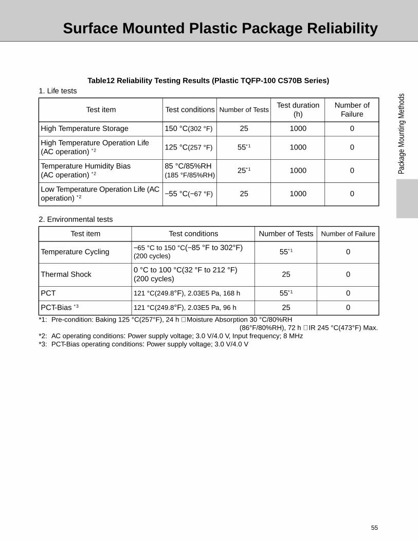
Table12 Reliability Testing Results (Plastic TQFP-100 CS70B Series) 1. Life tests
2. Environmental tests
*1: Pre-condition: Baking 125 °C(257°F), 24 h + Moisture Absorption 30 °C/80%RH(86°F/80%RH), 72 h + IR 245 °C(473°F) Max.
*2: AC operating conditions: Power supply voltage; 3.0 V/4.0 V, Input frequency; 8 MHz*3: PCT-Bias operating conditions: Power supply voltage; 3.0 V/4.0 V
Test item Test conditions Number of TestsTest duration
(h)Number of
Failure
High Temperature Storage 150 °C(302 °F) 25 1000 0
High Temperature Operation Life (AC operation) ∗2 125 °C(257 °F) 55∗1 1000 0
Temperature Humidity Bias(AC operation) ∗2
85 °C/85%RH(185 °F/85%RH)
25∗1 1000 0
Low Temperature Operation Life (AC operation) ∗2 −55 °C(−67 °F) 25 1000 0
Test item Test conditions Number of Tests Number of Failure
Temperature Cycling −65 °C to 150 °C(−85 °F to 302°F)(200 cycles)
55∗1 0
Thermal Shock0 °C to 100 °C(32 °F to 212 °F)(200 cycles)
25 0
PCT 121 °C(249.8°F), 2.03E5 Pa, 168 h 55∗1 0
PCT-Bias ∗3 121 °C(249.8°F), 2.03E5 Pa, 96 h 25 0
Surface Mounted Plastic Package Reliability
56
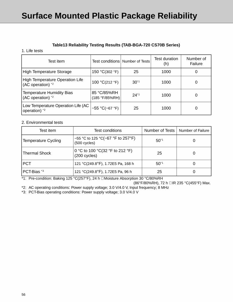
Table13 Reliability Testing Results (TAB-BGA-720 CS70B Series) 1. Life tests
2. Environmental tests
*1: Pre-condition: Baking 125 °C(257°F), 24 h + Moisture Absorption 30 °C/80%RH(86°F/80%RH), 72 h + IR 235 °C(455°F) Max.
*2: AC operating conditions: Power supply voltage; 3.0 V/4.0 V, Input frequency; 8 MHz*3: PCT-Bias operating conditions: Power supply voltage; 3.0 V/4.0 V
Test item Test conditions Number of TestsTest duration
(h)Number of
Failure
High Temperature Storage 150 °C(302 °F) 25 1000 0
High Temperature Operation Life (AC operation) ∗2 100 °C(212 °F) 30∗1 1000 0
Temperature Humidity Bias(AC operation) ∗2
85 °C/85%RH(185 °F/85%RH)
24∗1 1000 0
Low Temperature Operation Life (AC operation) ∗2 −55 °C(−67 °F) 25 1000 0
Test item Test conditions Number of Tests Number of Failure
Temperature Cycling −55 °C to 125 °C(−67 °F to 257°F)(500 cycles)
50∗1 0
Thermal Shock0 °C to 100 °C(32 °F to 212 °F)(200 cycles)
25 0
PCT 121 °C(249.8°F), 1.72E5 Pa, 168 h 50∗1 0
PCT-Bias ∗3 121 °C(249.8°F), 1.72E5 Pa, 96 h 25 0
Surface Mounted Plastic Package Reliability
57
Pack
age
Mou
ntin
g M
etho
ds
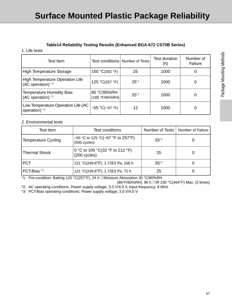
Table14 Reliability Testing Results (Enhanced BGA-672 CS70B Series) 1. Life tests
2. Environmental tests
*1: Pre-condition: Baking 125 °C(257°F), 24 h + Moisture Absorption 30 °C/80%RH(86°F/80%RH), 96 h + IR 230 °C(464°F) Max. (3 times)
*2: AC operating conditions: Power supply voltage; 3.0 V/4.0 V, Input frequency; 8 MHz*3: PCT-Bias operating conditions: Power supply voltage; 3.0 V/4.0 V
Test item Test conditions Number of TestsTest duration
(h)Number of
Failure
High Temperature Storage 150 °C(302 °F) 25 1000 0
High Temperature Operation Life (AC operation) ∗2 125 °C(257 °F) 25∗1 1000 0
Temperature Humidity Bias(AC operation) ∗2
85 °C/85%RH(185 °F/85%RH)
25∗1 1000 0
Low Temperature Operation Life (AC operation) ∗2 −55 °C(−67 °F) 12 1000 0
Test item Test conditions Number of Tests Number of Failure
Temperature Cycling −55 °C to 125 °C(−67 °F to 257°F)(500 cycles)
55∗1 0
Thermal Shock0 °C to 100 °C(32 °F to 212 °F)(200 cycles)
25 0
PCT 121 °C(249.8°F), 1.72E5 Pa, 168 h 55∗1 0
PCT-Bias ∗3 121 °C(249.8°F), 1.72E5 Pa, 72 h 25 0
Surface Mounted Plastic Package Reliability
58
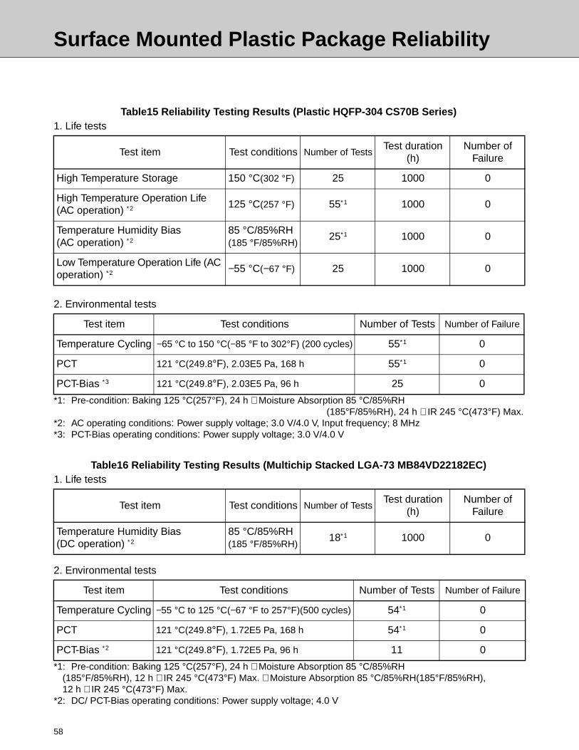
Table15 Reliability Testing Results (Plastic HQFP-304 CS70B Series) 1. Life tests
2. Environmental tests
*1: Pre-condition: Baking 125 °C(257°F), 24 h + Moisture Absorption 85 °C/85%RH(185°F/85%RH), 24 h + IR 245 °C(473°F) Max.
*2: AC operating conditions: Power supply voltage; 3.0 V/4.0 V, Input frequency; 8 MHz*3: PCT-Bias operating conditions: Power supply voltage; 3.0 V/4.0 V
Table16 Reliability Testing Results (Multichip Stacked LGA-73 MB84VD22182EC) 1. Life tests
2. Environmental tests
*1: Pre-condition: Baking 125 °C(257°F), 24 h + Moisture Absorption 85 °C/85%RH(185°F/85%RH), 12 h + IR 245 °C(473°F) Max. + Moisture Absorption 85 °C/85%RH(185°F/85%RH), 12 h + IR 245 °C(473°F) Max.
*2: DC/ PCT-Bias operating conditions: Power supply voltage; 4.0 V
Test item Test conditions Number of TestsTest duration
(h)Number of
Failure
High Temperature Storage 150 °C(302 °F) 25 1000 0
High Temperature Operation Life (AC operation) ∗2 125 °C(257 °F) 55∗1 1000 0
Temperature Humidity Bias(AC operation) ∗2
85 °C/85%RH(185 °F/85%RH)
25∗1 1000 0
Low Temperature Operation Life (AC operation) ∗2 −55 °C(−67 °F) 25 1000 0
Test item Test conditions Number of Tests Number of Failure
Temperature Cycling −65 °C to 150 °C(−85 °F to 302°F) (200 cycles) 55∗1 0
PCT 121 °C(249.8°F), 2.03E5 Pa, 168 h 55∗1 0
PCT-Bias ∗3 121 °C(249.8°F), 2.03E5 Pa, 96 h 25 0
Test item Test conditions Number of TestsTest duration
(h)Number of
Failure
Temperature Humidity Bias(DC operation) ∗2
85 °C/85%RH(185 °F/85%RH)
18∗1 1000 0
Test item Test conditions Number of Tests Number of Failure
Temperature Cycling −55 °C to 125 °C(−67 °F to 257°F)(500 cycles) 54∗1 0
PCT 121 °C(249.8°F), 1.72E5 Pa, 168 h 54∗1 0
PCT-Bias ∗2 121 °C(249.8°F), 1.72E5 Pa, 96 h 11 0
Storage
59
Pack
age
Mou
ntin
g M
etho
ds
2.4 Storage
Products should be stored while still packed in the materials that they were shipped in from Fujitsu.
• Befor open Dry Package, the recommended condition for the storage area is as below;Room Temperature; 5 to 30°C (41 to 86°F)Room Humidity; 70%RH or less
After open Dry Package, the recommended condition for the storage area is as below;Room Temperature; 5 to 30°C (41 to 86°F)Room Humidity; 40%RH to 70%RH
• Do not store the products where they will be exposed to corrosive gases or in dusty locations.
• Because sudden temperature changes can cause moisture to condense on the products,store the products in an area where the temperature remains fairly constant.
• Note that if products are stored for an extended period of time, the solderability of the leadpins may decline, rust may form, or the electrical characteristics may deteriorate.

MEMO