Embed Size (px)
Citation preview
DB81-10002-2E 1
Package Lineup/ Forms/ Structures
1. Package Lineup
2. Package Forms
3. Package Structures
2 DB81-10002-2E
Package Lineup/ Forms/ Structures1. Package Lineup PACKAGE
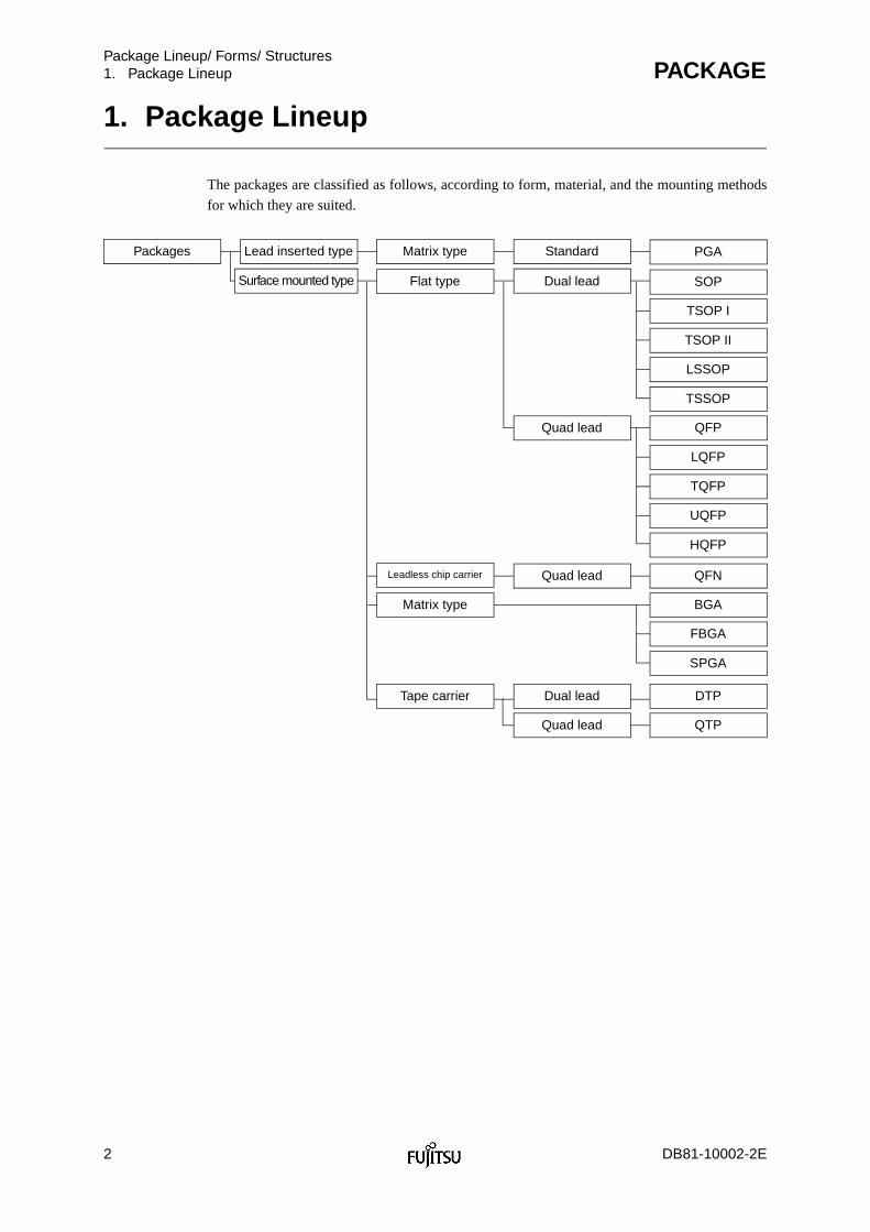
1. Package Lineup
The packages are classified as follows, according to form, material, and the mounting methods
for which they are suited.
Packages Lead inserted type PGA
SOP
TSOP I
TSOP II
LSSOP
TSSOP
QFP
LQFP
TQFP
UQFP
HQFP
QFN
BGA
SPGA
DTP
QTP
Standard
Dual lead
Quad lead
Quad lead
Dual lead
Quad lead
Matrix type
Flat typeSurface mounted type
Leadless chip carrier
Matrix type
Tape carrier
FBGA
DB81-10002-2E 3
Package Lineup/ Forms/ StructuresPACKAGE 1. Package Lineup
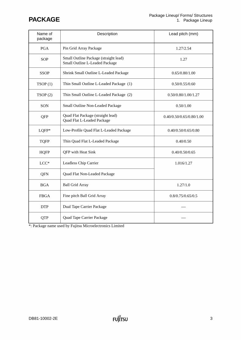
*: Package name used by Fujitsu Microelectronics Limited
Name of package
Description Lead pitch (mm)
PGA Pin Grid Array Package 1.27/2.54
SOP Small Outline Package (straight lead)Small Outline L-Leaded Package
1.27
SSOP Shrink Small Outline L-Leaded Package 0.65/0.80/1.00
TSOP (1) Thin Small Outline L-Leaded Package (1) 0.50/0.55/0.60
TSOP (2) Thin Small Outline L-Leaded Package (2) 0.50/0.80/1.00/1.27
SON Small Outline Non-Leaded Package 0.50/1.00
QFP Quad Flat Package (straight lead)Quad Flat L-Leaded Package
0.40/0.50/0.65/0.80/1.00
LQFP* Low-Profile Quad Flat L-Leaded Package 0.40/0.50/0.65/0.80
TQFP Thin Quad Flat L-Leaded Package 0.40/0.50
HQFP QFP with Heat Sink 0.40/0.50/0.65
LCC* Leadless Chip Carrier 1.016/1.27
QFN Quad Flat Non-Leaded Package
BGA Ball Grid Array 1.27/1.0
FBGA Fine pitch Ball Grid Array 0.8/0.75/0.65/0.5
DTP Dual Tape Carrier Package ⎯
QTP Quad Tape Carrier Package ⎯
4 DB81-10002-2E
Package Lineup/ Forms/ Structures2. Package Forms PACKAGE
2. Package Forms
Packages can be broadly classified into two types according to the mounting method used:
Lead inserted type: The leads on the package are inserted into through holes in a printed
circuit board, etc., and then soldered in place.
Surface mounted type: The device lays flat on surface of the circuit board and the leads are
soldered directly to the wires.
In addition, each of the various package forms has its own unique features.
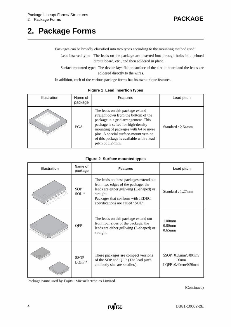
Figure 1 Lead insertion types
Figure 2 Surface mounted types
Package name used by Fujitsu Microelectronics Limited.
(Continued)
Illustration Name of package
Features Lead pitch
PGA
The leads on this package extend straight down from the bottom of the package in a grid arrangement. This package is suited for high-density mounting of packages with 64 or more pins. A special surface-mount version of this package is available with a lead pitch of 1.27mm.
Standard : 2.54mm
IllustrationName of package
Features Lead pitch
SOPSOL *
The leads on these packages extend out from two edges of the package; the leads are either gullwing (L-shaped) or straight.Packages that conform with JEDEC specifications are called "SOL".
Standard : 1.27mm
QFP
The leads on this package extend out from four sides of the package; the leads are either gullwing (L-shaped) or straight.
1.00mm0.80mm0.65mm
SSOPLQFP *
These packages are compact versions of the SOP and QFP. (The lead pitch and body size are smaller.)
SSOP : 0.65mm/0.80mm/1.00mm
LQFP : 0.40mm/0.50mm
DB81-10002-2E 5
Package Lineup/ Forms/ StructuresPACKAGE 2. Package Forms
(continued)
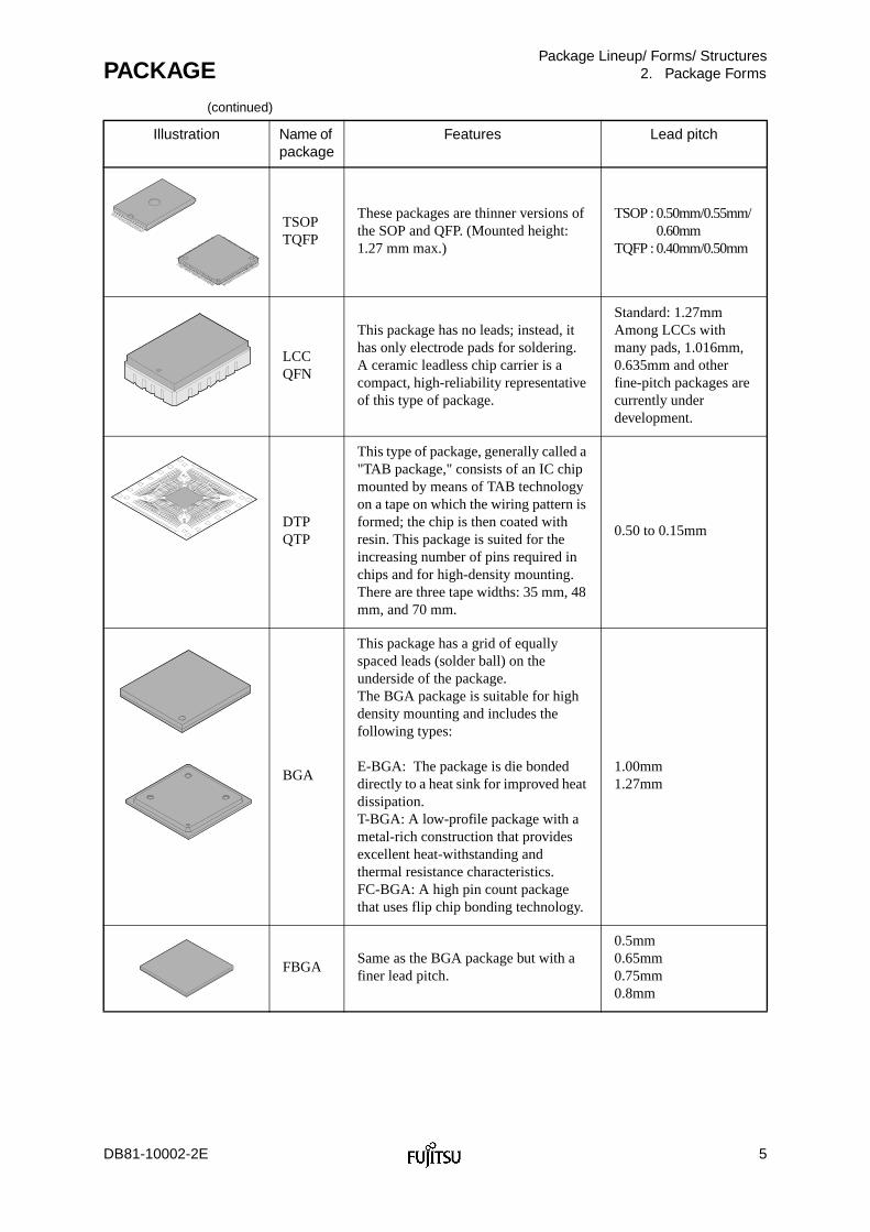
Illustration Name of package
Features Lead pitch
TSOPTQFP
These packages are thinner versions of the SOP and QFP. (Mounted height: 1.27 mm max.)
TSOP : 0.50mm/0.55mm/0.60mm
TQFP : 0.40mm/0.50mm
LCCQFN
This package has no leads; instead, it has only electrode pads for soldering. A ceramic leadless chip carrier is a compact, high-reliability representative of this type of package.
Standard: 1.27mmAmong LCCs with many pads, 1.016mm, 0.635mm and other fine-pitch packages are currently under development.
DTPQTP
This type of package, generally called a "TAB package," consists of an IC chip mounted by means of TAB technology on a tape on which the wiring pattern is formed; the chip is then coated with resin. This package is suited for the increasing number of pins required in chips and for high-density mounting. There are three tape widths: 35 mm, 48 mm, and 70 mm.
0.50 to 0.15mm
BGA
This package has a grid of equally spaced leads (solder ball) on the underside of the package.The BGA package is suitable for high density mounting and includes the following types:
E-BGA: The package is die bonded directly to a heat sink for improved heat dissipation.T-BGA: A low-profile package with a metal-rich construction that provides excellent heat-withstanding and thermal resistance characteristics.FC-BGA: A high pin count package that uses flip chip bonding technology.
1.00mm1.27mm
FBGASame as the BGA package but with a finer lead pitch.
0.5mm0.65mm0.75mm0.8mm
JAPAN
160-01
6 DB81-10002-2E
Package Lineup/ Forms/ Structures3. Package Structures PACKAGE
3. Package Structures
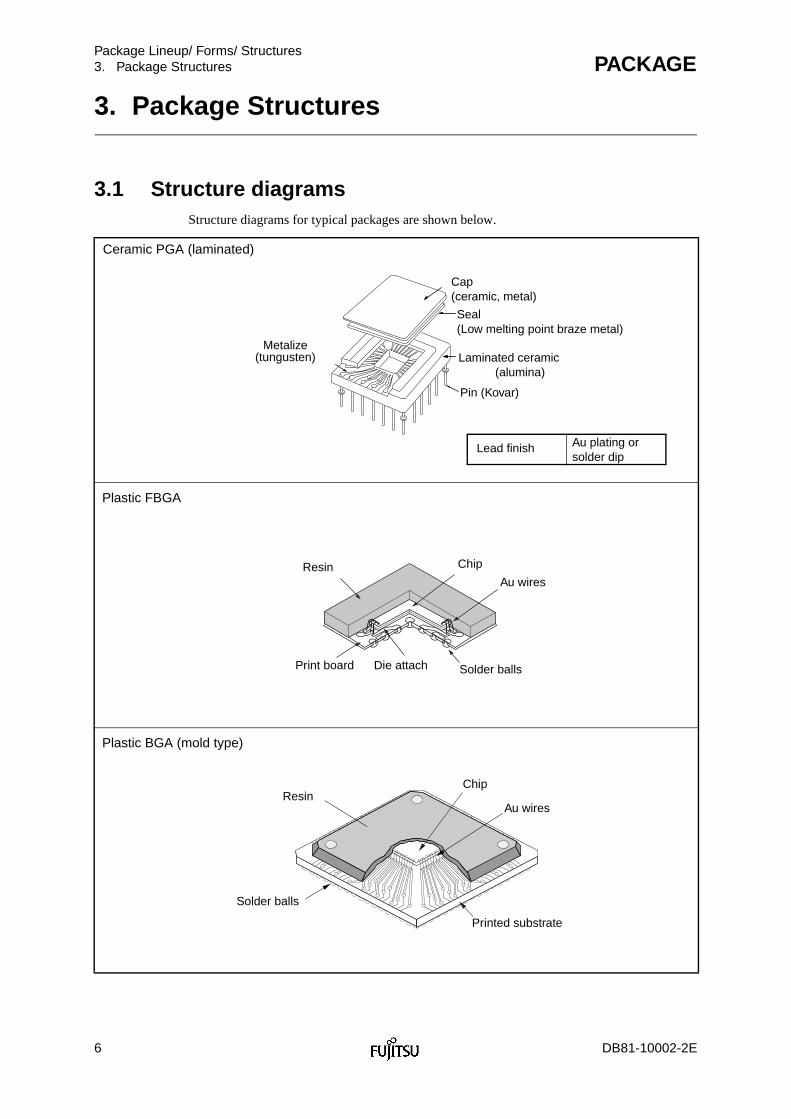
3.1 Structure diagramsStructure diagrams for typical packages are shown below.
Ceramic PGA (laminated)
Pin (Kovar)
Laminated ceramic(alumina)
Metalize(tungusten)
Cap(ceramic, metal)
Seal(Low melting point braze metal)
Lead finish Au plating or solder dip
Plastic FBGA
Print board Solder ballsDie attach
Resin Chip
Au wires
Plastic BGA (mold type)
Resin
Solder balls
Chip
Au wires
Printed substrate
DB81-10002-2E 7
Package Lineup/ Forms/ StructuresPACKAGE 3. Package Structures
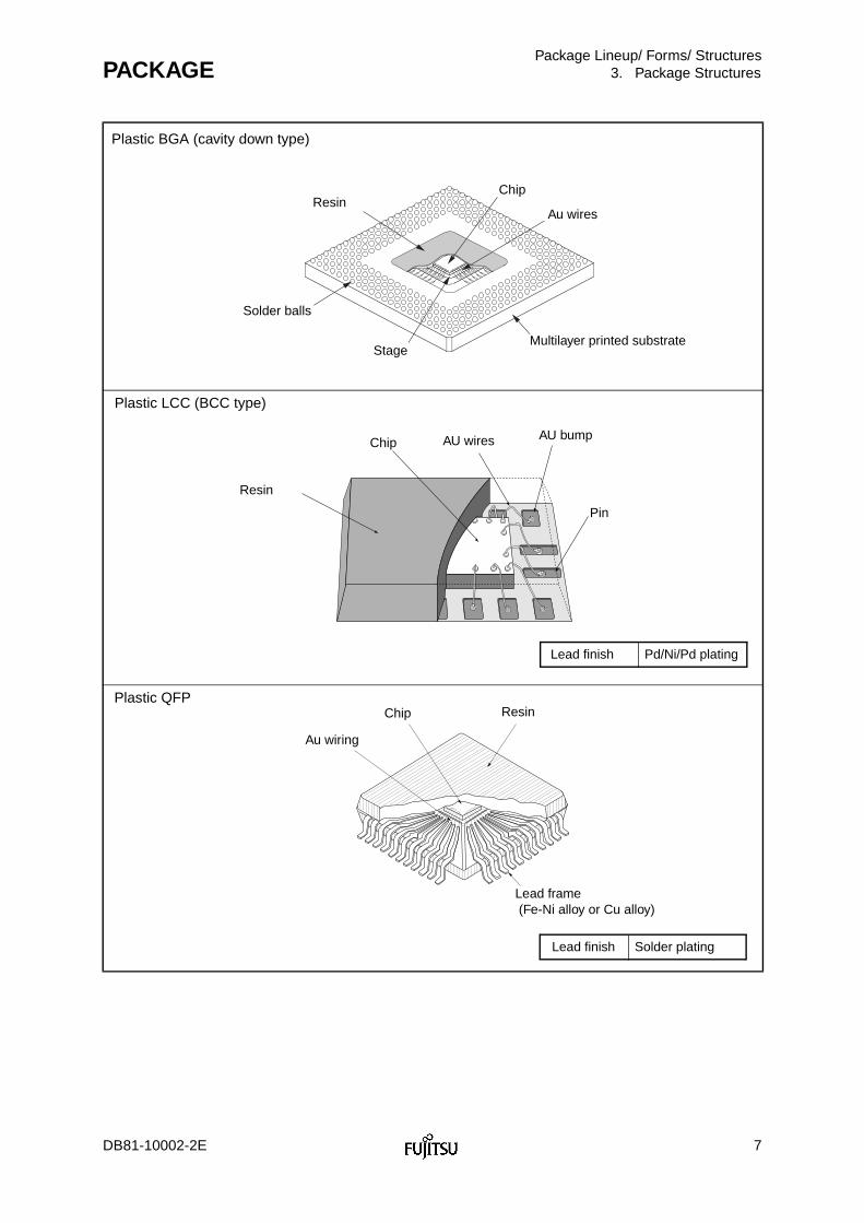
Plastic BGA (cavity down type)
ResinChip
Au wires
Solder balls
StageMultilayer printed substrate
Plastic LCC (BCC type)
Resin
Chip AU wires AU bump
Pin
Lead finish Pd/Ni/Pd plating
Plastic QFP
Au wiring
ResinChip
Lead frame (Fe-Ni alloy or Cu alloy)
Lead finish Solder plating
8 DB81-10002-2E
Package Lineup/ Forms/ Structures3. Package Structures PACKAGE
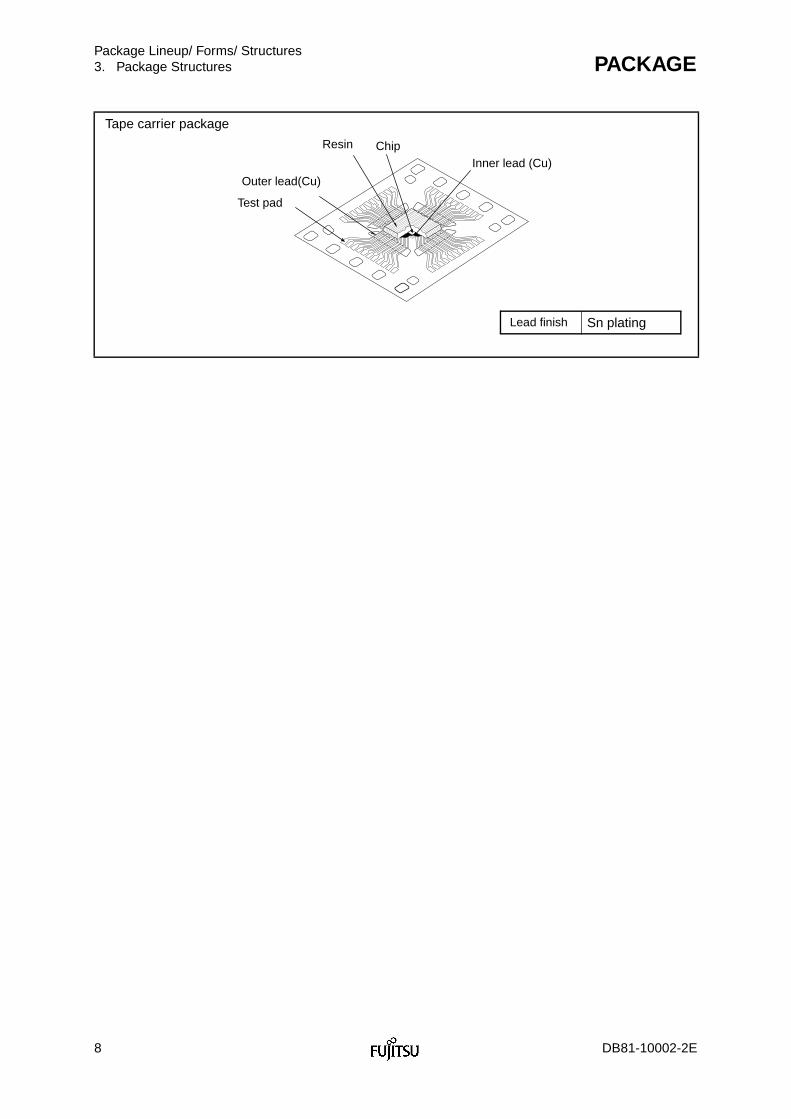
Tape carrier package
ChipResin
Outer lead(Cu)
Test pad
Inner lead (Cu)
Lead finish Sn plating
DB81-10002-2E 9
Package Lineup/ Forms/ StructuresPACKAGE 3. Package Structures
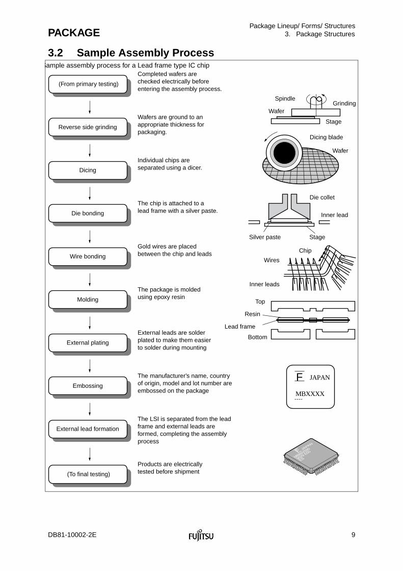
3.2 Sample Assembly Process
F JAPAN
MBXXXX
Sample assembly process for a Lead frame type IC chipCompleted wafers are checked electrically before entering the assembly process.
Wafers are ground to an appropriate thickness for packaging.
Individual chips are separated using a dicer.
The chip is attached to a lead frame with a silver paste.
Gold wires are placed between the chip and leads
The package is molded using epoxy resin
External leads are solder plated to make them easier to solder during mounting
The manufacturer’s name, country of origin, model and lot number are embossed on the package
The LSI is separated from the lead frame and external leads are formed, completing the assembly process
Products are electrically tested before shipment
(From primary testing)
Reverse side grinding
Dicing
Die bonding
Wire bonding
Molding
External plating
Embossing
External lead formation
(To final testing)
Spindle
WaferGrinding
Stage
Dicing blade
Wafer
Die collet
Inner lead
StageSilver paste
Chip
Wires
Inner leads
Resin
Lead frame
Top
Bottom
10 DB81-10002-2E
Package Lineup/ Forms/ Structures3. Package Structures PACKAGE
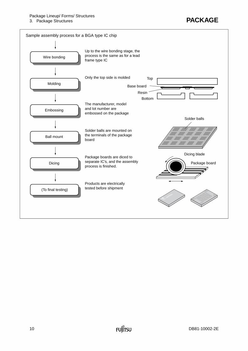
Sample assembly process for a BGA type IC chip
Up to the wire bonding stage, the process is the same as for a lead frame type IC
Only the top side is molded
The manufacturer, model and lot number are embossed on the package
Solder balls are mounted on the terminals of the package board
Package boards are diced to separate IC’s, and the assembly process is finished.
Products are electrically tested before shipment
Wire bonding
Molding
Embossing
Ball mount
Dicing
(To final testing)
Top
Bottom
Resin
Base board
Solder balls
Dicing blade
Package board
DB81-10002-2E 11
Package Lineup/ Forms/ StructuresPACKAGE 3. Package Structures
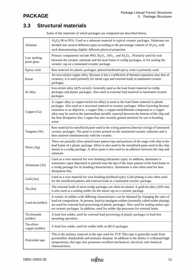
3.3 Structural materialsSome of the materials of which packages are composed are described below.
AluminaAl2O3 90 to 95%. Used as a substrate material in typical ceramic packages. Substrates are divided into several different types according to the percentage content of Al2O3, with each demonstrating slightly different physical properties.
Low melting point glass
Primary components include PbO, B2O3 , SiO2 , and Al2O3 . Primarily used for seal between the ceramic substrate and the lead frame in cerdip packages, or for sealing the ceramic cap on a laminated ceramic package.
Epoxy resin Raw material for plastic packages; phenol-hardened epoxy resin is primarily used.
KovarAn iron-nickel-copper alloy. Because it has a coefficient of thermal expansion near that of ceramics, it is used primarily for metal caps and external leads in laminated ceramic packages.
42 alloyIron-nickel alloy (42% nickel). Generally used as the lead frame material in cerdip packages and plastic packages. Also used as external lead material in laminated ceramic packages.
Copper (Cu)
A copper alloy (a copper-nickel-tin alloy) is used as the lead frame material in plastic packages. Also used as a structural material in ceramic packages. When lowering thermal resistance is an objective, a copper film, a copper-molybdenum compound or a copper alloy may be used as the intermediate metallic material between the bottom of the chip and the heat dissipation fins. Copper has also recently gained attention for use in bonding wires.
Tungsten (W)Raw material for metallized paste used in the wiring patterns (internal wiring) of laminated ceramic packages. The paste is screen printed on the unsintered ceramic substrate and is then sintered simultaneously with the ceramic.
Silver (Ag)
There are partially silver-plated inner pattern tips and portions of the stage with chip in the lead frame of a plastic package. Silver is also used in the metallized paste used in the chip mount in a cerdip package. A silver paste is also used as an adhesive between the chip and substrate.
Aluminum (Al)
Used as a wire material for wire bonding (ultrasonic type). In addition, aluminum is sometimes vapor deposited or pressed onto the tips of the inner pattern of the lead frame in a cerdip package for its bonding characteristics. Aluminum is also often used for heat dissipation fins.
Gold (Au)Used as a wire material for wire bonding (nailhead type). Gold plating is also often used for the metallized pattern and external leads in a laminated ceramic package.
Tin (Sn)The external leads of most cerdip packages are often tin-plated. A gold-tin alloy (20% tin) is also used as a sealing solder for the metal cap on a ceramic package.
Lead-tin (solder)
A variety of solders with differing characteristics can be obtained by changing the ratio of lead-tin composition. At present, lead-tin amalgam solders (normally called solder plating) are used for external lead processing of plastic packages. Also used for sealing metal caps on ceramic packages. In addition, used for solder dip processes for external leads.
Tin-bismuth (solder)
A lead-free solder, used for external lead processing of plastic packages in lead-free mounting operation.
Tin-silver-copper (solder)
A lead-free solder, used for solder balls on BGA packages.
Polyimide tape
This is the primary material in the tape used for TCP. This tape is generally made from pyromellitic dianhydride and aromatic diamine. In addition to the ability to withstand high temperatures, this tape also possesses excellent mechanical, electrical, and chemical characteristics.
12 DB81-10002-2E
Package Lineup/ Forms/ Structures3. Package Structures PACKAGE
■ Lead-Free PackagesThe use of lead-free electronic components is mentioned as a significant issue in global
environment assessments.
Lead is a harmful heavy metal, which if absorbed and accumulated in the body is reported to
cause damage including inhibited growth in children and psychological damage in adults.
In particular, lead can leach from electronic products that have been disposed of in land fills,
from contact with acid rainwater. This can lead to contamination of rivers and ground water,
and can thereby enter the body through drinking water.
At Fujitsu, we have actively addressed this problem by starting the production of lead-free
products with semiconductor packages completely free of lead as of October, 2000.
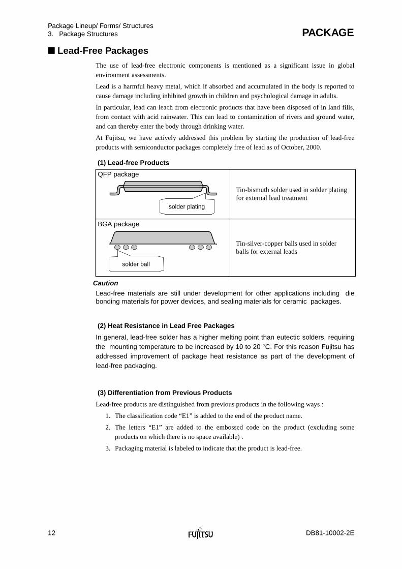
(1) Lead-free Products
Caution
Lead-free materials are still under development for other applications including diebonding materials for power devices, and sealing materials for ceramic packages.
(2) Heat Resistance in Lead Free Packages
In general, lead-free solder has a higher melting point than eutectic solders, requiringthe mounting temperature to be increased by 10 to 20 °C. For this reason Fujitsu hasaddressed improvement of package heat resistance as part of the development oflead-free packaging.
(3) Differentiation from Previous Products
Lead-free products are distinguished from previous products in the following ways :
1. The classification code “E1” is added to the end of the product name.
2. The letters “E1” are added to the embossed code on the product (excluding some
products on which there is no space available) .
3. Packaging material is labeled to indicate that the product is lead-free.
QFP package
Tin-bismuth solder used in solder plating for external lead treatment
BGA package
Tin-silver-copper balls used in solder balls for external leads
solder plating
solder ball