Embed Size (px)
Citation preview
1 Publication Order Number:P6SMB6.8AT3/D
P6SMB6.8AT3G Series,SZP6SMB6.8AT3G Series
600 Watt Peak Power ZenerTransient VoltageSuppressors
Unidirectional*
The SMB series is designed to protect voltage sensitivecomponents from high voltage, high energy transients. They haveexcellent clamping capability, high surge capability, low zenerimpedance and fast response time. The SMB series is supplied inthe Littelfuse exclusive, cost-effective, highly reliable package and is ideal ly sui ted for use in communication systems, automotive, numerical controls, process controls, medical equipment, business machines, power supplies and many other industrial/consumer applications.
Specification Features:• Working Peak Reverse Voltage Range − 5.8 to 171 V
• Standard Zener Breakdown Voltage Range − 6.8 to 200 V
• Peak Power − 600 W @ 1 ms
• ESD Rating of Class 3 (> 16 kV) per Human Body Model
• Maximum Clamp Voltage @ Peak Pulse Current
• Low Leakage < 5 �A Above 10 V
• UL 497B for Isolated Loop Circuit Protection
• Response Time is Typically < 1 ns
• SZ Prefix for Automotive and Other Applications Requiring UniqueSite and Control Change Requirements; AEC−Q101 Qualified andPPAP Capable
• These Devices are Pb−Free and are RoHS Compliant
Mechanical Characteristics:CASE: Void-free, transfer-molded, thermosetting plasticFINISH: All external surfaces are corrosion resistant and leads are
readily solderableMAXIMUM CASE TEMPERATURE FOR SOLDERING PURPOSES:
260°C for 10 SecondsLEADS: Modified L−Bend providing more contact area to bond padsPOLARITY: Cathode indicated by polarity bandMOUNTING POSITION: Any
*Please see P6SMB11CAT3 to P6SMB91CAT3 for Bidirectional devices.
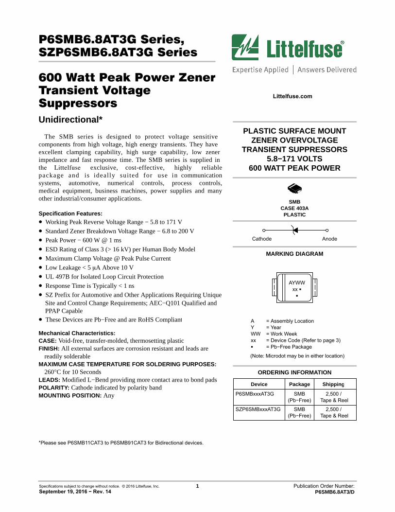
PLASTIC SURFACE MOUNTZENER OVERVOLTAGE
TRANSIENT SUPPRESSORS5.8−171 VOLTS
600 WATT PEAK POWER
Cathode Anode
Device Package Shipping
ORDERING INFORMATION
SMBCASE 403A
PLASTIC
P6SMBxxxAT3G SMB(Pb−Free)
2,500 / Tape & Reel
A = Assembly LocationY = YearWW = Work Weekxx = Device Code (Refer to page 3)� = Pb−Free Package
MARKING DIAGRAM
(Note: Microdot may be in either location)
AYWWxx ��
SZP6SMBxxxAT3G SMB(Pb−Free)
2,500 / Tape & Reel
Littelfuse.com
Specifications subject to change without notice. © 2016 Littelfuse, Inc.September 19, 2016 − Rev. 14
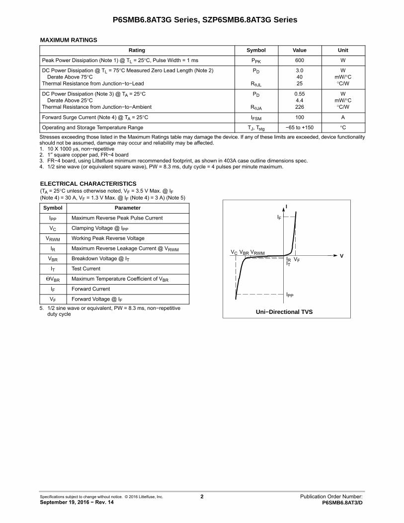
Uni−Directional TVS
IPP
IF
V
I
IRIT
VRWMVC VBRVF
P6SMB6.8AT3G Series, SZP6SMB6.8AT3G Series
MAXIMUM RATINGS
Rating Symbol Value Unit
Peak Power Dissipation (Note 1) @ TL = 25°C, Pulse Width = 1 ms PPK 600 W
DC Power Dissipation @ TL = 75°C Measured Zero Lead Length (Note 2)Derate Above 75°C
Thermal Resistance from Junction−to−Lead
PD
R�JL
3.04025
WmW/°C°C/W
DC Power Dissipation (Note 3) @ TA = 25°CDerate Above 25°C
Thermal Resistance from Junction−to−Ambient
PD
R�JA
0.554.4226
WmW/°C°C/W
Forward Surge Current (Note 4) @ TA = 25°C IFSM 100 A
Operating and Storage Temperature Range TJ, Tstg −65 to +150 °C
Stresses exceeding those listed in the Maximum Ratings table may damage the device. If any of these limits are exceeded, device functionalityshould not be assumed, damage may occur and reliability may be affected.1. 10 X 1000 �s, non−repetitive2. 1″ square copper pad, FR−4 board3. FR−4 board, using Littelfuse minimum recommended footprint, as shown in 403A case outline dimensions spec.4. 1/2 sine wave (or equivalent square wave), PW = 8.3 ms, duty cycle = 4 pulses per minute maximum.
ELECTRICAL CHARACTERISTICS(TA = 25°C unless otherwise noted, VF = 3.5 V Max. @ IF(Note 4) = 30 A, VF = 1.3 V Max. @ IF (Note 4) = 3 A) (Note 5)
Symbol Parameter
IPP Maximum Reverse Peak Pulse Current
VC Clamping Voltage @ IPP
VRWM Working Peak Reverse Voltage
IR Maximum Reverse Leakage Current @ VRWM
VBR Breakdown Voltage @ IT
IT Test Current
�VBR Maximum Temperature Coefficient of VBR
IF Forward Current
VF Forward Voltage @ IF5. 1/2 sine wave or equivalent, PW = 8.3 ms, non−repetitive
duty cycle
2 Publication Order Number:P6SMB6.8AT3/D
Specifications subject to change without notice. © 2016 Littelfuse, Inc.September 19, 2016 − Rev. 14
P6SMB6.8AT3G Series, SZP6SMB6.8AT3G Series
ELECTRICAL CHARACTERISTICS
Device*Device
Marking
VRWM(Note 6)
IR @VRWM
Breakdown Voltage VC @ IPP (Note 8)
�VBR
Ctyp(Note 9)VBR V (Note 7) @ IT VC IPP
V �A Min Nom Max mA V A %/°C pF
P6SMB6.8AT3GP6SMB7.5AT3GP6SMB8.2AT3GP6SMB9.1AT3G
6V8A7V5A8V2A9V1A
5.86.47.027.78
100050020050
6.457.137.798.65
6.87.518.29.1
7.147.888.619.55
1010101
10.511.312.113.4
57535045
0.0570.0610.0650.068
2380218020151835
P6SMB10AT3GP6SMB12AT3GP6SMB13AT3G
10A12A13A
8.5510.211.1
1055
9.511.412.4
1012
13.05
10.512.613.7
111
14.516.718.2
413633
0.0730.0780.081
169014351335
P6SMB15AT3GP6SMB16AT3GP6SMB18AT3GP6SMB20AT3G
15A16A18A20A
12.813.615.317.1
5555
14.315.217.119
15.05161820
15.816.818.921
1111
21.222.525.227.7
28272422
0.0840.0860.0880.09
117511101000910
P6SMB22AT3GP6SMB24AT3GP6SMB27AT3GP6SMB30AT3G
22A24A27A30A
18.820.523.125.6
5555
20.922.825.728.5
2224
27.0530
23.125.228.431.5
1111
30.633.237.541.4
201816
14.4
0.0920.0940.0960.097
835775700635
P6SMB33AT3GP6SMB36AT3GP6SMB39AT3GP6SMB43AT3G
33A36A39A43A
28.230.833.336.8
5555
31.434.237.140.9
33.0536
39.0543.05
34.737.841
45.2
1111
45.749.953.959.3
13.212
11.210.1
0.0980.0990.1
0.101
585540500460
P6SMB47AT3GP6SMB51AT3GP6SMB56AT3GP6SMB62AT3G
47A51A56A62A
40.243.647.853
5555
44.748.553.258.9
47.0551.05
5662
49.453.658.865.1
1111
64.870.17785
9.38.67.87.1
0.1010.1020.1030.104
425395365335
P6SMB68AT3GP6SMB75AT3GP6SMB91AT3G
68A75A91A
58.164.177.8
555
64.671.386.5
6875.05
91
71.478.895.5
111
92103125
6.55.84.8
0.1040.1050.106
305280235
P6SMB100AT3GP6SMB120AT3GP6SMB130AT3G
100A120A130A
85.5102111
555
95114124
100120
130.5
105126137
111
137165179
4.43.63.3
0.1060.1070.107
215185170
P6SMB150AT3GP6SMB160AT3GP6SMB180AT3G
150A160A180A
128136154
555
143152171
150.5160180
158168189
111
207219246
2.92.72.4
0.1080.1080.108
150140130
P6SMB200AT3G 200A 171 5 190 200 210 1 274 2.2 0.108 1156. A transient suppressor is normally selected according to the working peak reverse voltage (VRWM), which should be equal to or greater than
the DC or continuous peak operating voltage level.7. VBR measured at pulse test current IT at an ambient temperature of 25°C.8. Surge current waveform per Figure 2 and derate per Figure 3.9. Bias Voltage = 0 V, F = 1 MHz, TJ = 25°C* Include SZ-prefix devices where applicable.
3 Publication Order Number:P6SMB6.8AT3/D
Specifications subject to change without notice. © 2016 Littelfuse, Inc.September 19, 2016 − Rev. 14
P6SMB6.8AT3G Series, SZP6SMB6.8AT3G Series
P ,
PEAK
PO
WER
(kW
)P
NONREPETITIVEPULSE WAVEFORMSHOWN IN FIGURE 2
tP, PULSE WIDTH
1
10
100
0.1 �s 1 �s 10 �s 100 �s 1 ms 10 ms0.1
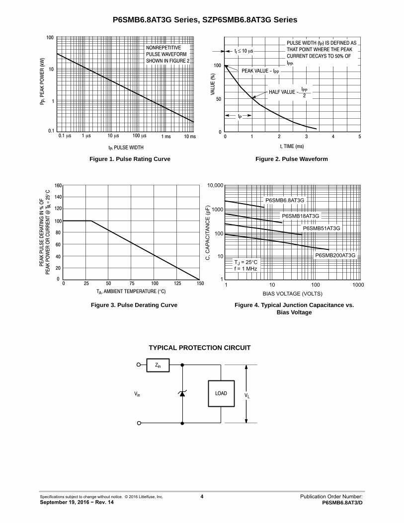
Figure 1. Pulse Rating Curve
0 1 2 3 40
50
100
t, TIME (ms)
VALU
E (%
)
HALF VALUE - IPP2
PEAK VALUE - IPP
tr�≤ 10 �s
Figure 2. Pulse Waveform
TYPICAL PROTECTION CIRCUIT
Vin VL
Zin
LOAD
Figure 3. Pulse Derating Curve
PEAK
PU
LSE
DER
ATIN
G IN
% O
FPE
AK P
OW
ER O
R C
UR
REN
T @
T A=
25C°
100
80
60
40
20
00 25 50 75 100 125 150
TA, AMBIENT TEMPERATURE (°C)
120
140
160
tP
PULSE WIDTH (tP) IS DEFINED ASTHAT POINT WHERE THE PEAKCURRENT DECAYS TO 50% OFIPP.
Figure 4. Typical Junction Capacitance vs.Bias Voltage
P6SMB6.8AT3G
P6SMB18AT3G
P6SMB51AT3G
P6SMB200AT3G
BIAS VOLTAGE (VOLTS)
1 10 100 1000
10
100
1000
10,000
C, C
APA
CIT
AN
CE
(pF)
1
5
TJ = 25°Cf = 1 MHz
4 Publication Order Number:P6SMB6.8AT3/D
Specifications subject to change without notice. © 2016 Littelfuse, Inc.September 19, 2016 − Rev. 14
P6SMB6.8AT3G Series, SZP6SMB6.8AT3G Series
APPLICATION NOTES
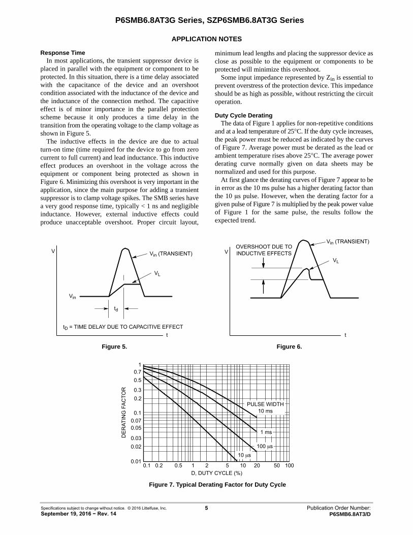
Response TimeIn most applications, the transient suppressor device is
placed in parallel with the equipment or component to beprotected. In this situation, there is a time delay associatedwith the capacitance of the device and an overshootcondition associated with the inductance of the device andthe inductance of the connection method. The capacitiveeffect is of minor importance in the parallel protectionscheme because it only produces a time delay in thetransition from the operating voltage to the clamp voltage asshown in Figure 5.
The inductive effects in the device are due to actualturn-on time (time required for the device to go from zerocurrent to full current) and lead inductance. This inductiveeffect produces an overshoot in the voltage across theequipment or component being protected as shown inFigure 6. Minimizing this overshoot is very important in theapplication, since the main purpose for adding a transientsuppressor is to clamp voltage spikes. The SMB series havea very good response time, typically < 1 ns and negligibleinductance. However, external inductive effects couldproduce unacceptable overshoot. Proper circuit layout,
minimum lead lengths and placing the suppressor device asclose as possible to the equipment or components to beprotected will minimize this overshoot.
Some input impedance represented by Zin is essential toprevent overstress of the protection device. This impedanceshould be as high as possible, without restricting the circuitoperation.
Duty Cycle DeratingThe data of Figure 1 applies for non-repetitive conditions
and at a lead temperature of 25°C. If the duty cycle increases,the peak power must be reduced as indicated by the curvesof Figure 7. Average power must be derated as the lead orambient temperature rises above 25°C. The average powerderating curve normally given on data sheets may benormalized and used for this purpose.
At first glance the derating curves of Figure 7 appear to bein error as the 10 ms pulse has a higher derating factor thanthe 10 �s pulse. However, when the derating factor for agiven pulse of Figure 7 is multiplied by the peak power valueof Figure 1 for the same pulse, the results follow theexpected trend.
VL
V
Vin
Vin (TRANSIENT)VL
td
V
Vin (TRANSIENT)OVERSHOOT DUE TOINDUCTIVE EFFECTS
tD = TIME DELAY DUE TO CAPACITIVE EFFECTt t
Figure 5. Figure 6.
Figure 7. Typical Derating Factor for Duty Cycle
DE
RAT
ING
FA
CTO
R
1 ms
10 �s
10.70.5
0.3
0.05
0.1
0.2
0.01
0.020.03
0.07
100 �s
0.1 0.2 0.5 2 5 10 501 20 100D, DUTY CYCLE (%)
PULSE WIDTH10 ms
5 Publication Order Number:P6SMB6.8AT3/D
Specifications subject to change without notice. © 2016 Littelfuse, Inc.September 19, 2016 − Rev. 14
P6SMB6.8AT3G Series, SZP6SMB6.8AT3G Series
UL RECOGNITION
The entire series has Underwriters LaboratoryRecognition for the classification of protectors (QVGQ2)under the UL standard for safety 497B and File .Many competitors only have one or two devices recognizedor have recognition in a non-protective category. Somecompetitors have no recognition at all. With the UL497Brecognition, our parts successfully passed several tests
including Strike Voltage Breakdown test, EnduranceConditioning, Temperature test, DielectricVoltage-Withstand test, Discharge test and several more.
Whereas, some competitors have only passed aflammability test for the package material, we have beenrecognized for much more to be included in their Protectorcategory.
6 Publication Order Number:P6SMB6.8AT3/D
Specifications subject to change without notice. © 2016 Littelfuse, Inc.September 19, 2016 − Rev. 14
#E128662
P6SMB6.8AT3G Series, SZP6SMB6.8AT3G Series
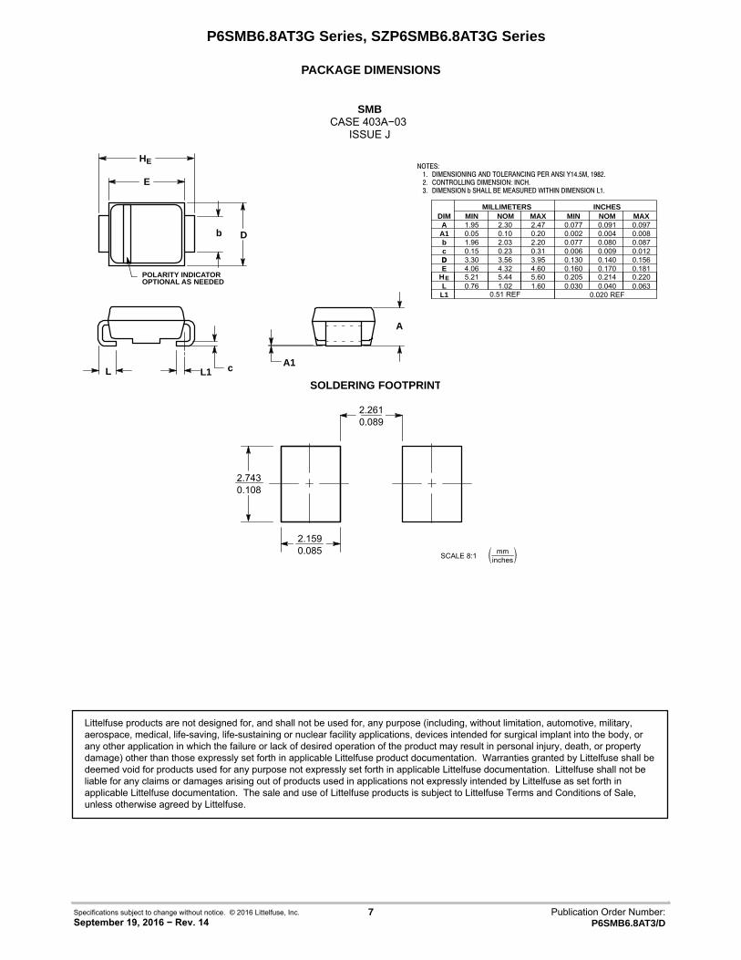
PACKAGE DIMENSIONS
SMBCASE 403A−03
ISSUE J
E
b D
cL1L
A
A1
NOTES:1. DIMENSIONING AND TOLERANCING PER ANSI Y14.5M, 1982.2. CONTROLLING DIMENSION: INCH.3. DIMENSION b SHALL BE MEASURED WITHIN DIMENSION L1.
2.2610.089
2.7430.108
2.1590.085 � mm
inches�SCALE 8:1
SOLDERING FOOTPRINT
DIMA
MIN NOM MAX MINMILLIMETERS
1.95 2.30 2.47 0.077
INCHES
A1 0.05 0.10 0.20 0.002b 1.96 2.03 2.20 0.077c 0.15 0.23 0.31 0.006D 3.30 3.56 3.95 0.130E 4.06 4.32 4.60 0.160
L 0.76 1.02 1.60 0.030
0.091 0.0970.004 0.0080.080 0.0870.009 0.0120.140 0.1560.170 0.181
0.040 0.063
NOM MAX
5.21 5.44 5.60 0.205 0.214 0.220HE
0.51 REF 0.020 REF
D
L1
HE
POLARITY INDICATOROPTIONAL AS NEEDED
7 Publication Order Number:P6SMB6.8AT3/D
Specifications subject to change without notice. © 2016 Littelfuse, Inc.September 19, 2016 − Rev. 14
Littelfuse products are not designed for, and shall not be used for, any purpose (including, without limitation, automotive, military, aerospace, medical, life-saving, life-sustaining or nuclear facility applications, devices intended for surgical implant into the body, or any other application in which the failure or lack of desired operation of the product may result in personal injury, death, or property damage) other than those expressly set forth in applicable Littelfuse product documentation. Warranties granted by Littelfuse shall be deemed void for products used for any purpose not expressly set forth in applicable Littelfuse documentation. Littelfuse shall not be liable for any claims or damages arising out of products used in applications not expressly intended by Littelfuse as set forth in applicable Littelfuse documentation. The sale and use of Littelfuse products is subject to Littelfuse Terms and Conditions of Sale, unless otherwise agreed by Littelfuse.