Embed Size (px)
Citation preview
© 2020 Littelfuse, Inc.Specifications are subject to change without notice.
Revised: BA.11/05/20
TVS DiodesSurface Mount – 400W > P4SMA series
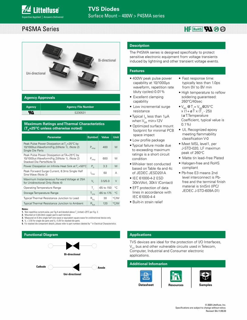
Description
Agency Approvals
Features
• 400W peak pulse power capability at 10/1000µs waveform, repetition rate (duty cycles):0.01%
• Excellent clamping capability
• Low incremental surge resistance
• Typical IR less than 1μA when VBR min>12V
• Optimized surface mount footprint for minimal PCB space impact
• Low profile package• Typical failure mode due
to exceeding maximum ratings is a short circuit condition
• Whisker test conducted based on Table 4a and 4c of JEDEC JESD201A
• IEC 61000-4-2 ESD 30kV(Air), 30kV (Contact)
• EFT protection of data lines in accordance with IEC 61000-4-4
• Built-in strain relief
• Fast response time: typically less than 1.0ps from 0V to BV min
• High temperature to reflow soldering guaranteed: 260°C/40sec
• VBR @ TJ= VBR@25°C x (1+αT x (TJ - 25))(αT:Temperature Coefficient, typical value is 0.1%)
• UL Recognized epoxy meeting flammability classification V-0
• Meet MSL level1, per J-STD-020, LF maximun peak of 260°C
• Matte tin lead–free Plated• Halogen-free and RoHS
compliant• Pb-free E3 means 2nd
level interconnect is Pb-free and the terminal finish material is tin(Sn) (IPC/JEDEC J-STD-609A.01)
Applications
TVS devices are ideal for the protection of I/O Interfaces, VCC bus and other vulnerable circuits used in Telecom, Computer, Industrial and Consumer electronic applications.
The P4SMA series is designed specifically to protect sensitive electronic equipment from voltage transients induced by lightning and other transient voltage events.
Maximum Ratings and Thermal Characteristics (TA=25OC unless otherwise noted)
Parameter Symbol Value Unit
Peak Pulse Power Dissipation at TA=25°C by 10/1000us Waveform(Fig.2)(Note 1), (Note 2)Single Die Parts
PPPM 400 W
Peak Pulse Power Dissipation at TA=25°C by 10/1000us Waveform(Fig.2)(Note 1), (Note 2) Stacked Die Parts(Note 5)
PPPM 600 W
Power Dissipation on Infinite Heat Sink at TL=50OC PD 3.3 W
Peak Forward Surge Current, 8.3ms Single Half Sine Wave (Note 3) IFSM 60 A
Maximum Instantaneous Forward Voltage at 25A for Unidirectional Only (Note 4) VF 3.5/5.0 V
Operating Temperature Range TJ -65 to 150 °C
Storage Temperature Range TSTG -65 to 175 °C
Typical Thermal Resistance Junction to Lead RθJL 30 °C/W
Typical Thermal Resistance Junction to Ambient RθJA 120 °C/W
Agency Agency File Number
E230531
P4SMA Series
Functional Diagram
Bi-directional
Uni-directional
Cathode Anode
Uni-directional
Bi-directional
RoHS Pb e3
Datasheet
Additional Infomarion
Resources Samples
Notes:1. Non-repetitive current pulse, per Fig.4 and derated above TJ (initial) =25ºC per Fig. 3.2. Mounted on 5.0x5.0mm copper pad to each terminal.3. Measured on 8.3ms single half sine wave or equivalent square wave for unidirectional device only.4. VF < 3.5V for single die parts and VF< 5.0V for stacked-die parts.5. For stacked die component details, please refer to part numbers labeled by * in Electrical Characteristics.

© 2020 Littelfuse, Inc.Specifications are subject to change without notice.
Revised: BA.11/05/20
TVS DiodesSurface Mount – 400W > P4SMA series
Electrical Characteristics (TA=25°C unless otherwise noted)
Part Number
(Uni)
Part Number
(Bi)
MarkingReverse
Stand offVoltage VR
(Volts)
Breakdown Voltage VBR
(Volts) @ IT
Test CurrentIT (mA)
Maximum Clamping Voltage VC @ Ipp (V)
Maximum Peak Pulse Current Ipp
(A)
Maximum Reverse
Leakage IR @ VR (µA)
Maximum Temperature Coefficient of
VBR (%/C)
Agency Approval
Uni Bi Min Max
P4SMA6.8A P4SMA6.8CA 6V8A 6V8C 5.80 6.45 7.14 10 10.5 39.0 1000 0.041 X
P4SMA7.5A P4SMA7.5CA 7V5A 7V5C 6.40 7.13 7.88 10 11.3 36.3 500 0.052 X
P4SMA8.2A P4SMA8.2CA 8V2A 8V2C 7.02 7.79 8.61 10 12.1 33.9 200 0.058 X
P4SMA9.1A P4SMA9.1CA 9V1A 9V1C 7.78 8.65 9.55 1 13.4 30.6 50 0.063 X
P4SMA10A P4SMA10CA 10A 10C 8.55 9.50 10.50 1 14.5 28.3 10 0.066 X
P4SMA11A P4SMA11CA 11A 11C 9.40 10.50 11.60 1 15.6 26.3 5 0.069 X
P4SMA12A P4SMA12CA 12A 12C 10.20 11.40 12.60 1 16.7 24.6 5 0.071 X
P4SMA13A P4SMA13CA 13A 13C 11.10 12.40 13.70 1 18.2 22.5 1 0.074 X
P4SMA15A P4SMA15CA 15A 15C 12.80 14.30 15.80 1 21.2 19.3 1 0.076 X
P4SMA16A P4SMA16CA 16A 16C 13.60 15.20 16.80 1 22.5 18.2 1 0.080 X
P4SMA18A P4SMA18CA 18A 18C 15.30 17.10 18.90 1 25.5 16.1 1 0.083 X
P4SMA20A P4SMA20CA 20A 20C 17.10 19.00 21.00 1 27.7 14.8 1 0.085 X
P4SMA22A P4SMA22CA 22A 22C 18.80 20.90 23.10 1 30.6 13.4 1 0.088 X
P4SMA24A P4SMA24CA 24A 24C 20.50 22.80 25.20 1 33.2 12.3 1 0.091 X
P4SMA27A P4SMA27CA 27A 27C 23.10 25.70 28.40 1 37.5 10.9 1 0.092 X
P4SMA30A P4SMA30CA 30A 30C 25.60 28.50 31.50 1 41.4 9.9 1 0.093 X
P4SMA33A P4SMA33CA 33A 33C 28.20 31.40 34.70 1 45.7 9.0 1 0.094 X
P4SMA36A P4SMA36CA 36A 36C 30.80 34.20 37.80 1 49.9 8.2 1 0.096 X
P4SMA39A P4SMA39CA 39A 39C 33.30 37.10 41.00 1 53.9 7.6 1 0.097 X
P4SMA43A P4SMA43CA 43A 43C 36.80 40.90 45.20 1 59.3 6.9 1 0.098 X
P4SMA47A P4SMA47CA 47A 47C 40.20 44.70 49.40 1 64.8 6.3 1 0.099 X
P4SMA51A P4SMA51CA 51A 51C 43.60 48.50 53.60 1 70.1 5.8 1 0.100 X
P4SMA56A P4SMA56CA 56A 56C 47.80 53.20 58.80 1 77.0 5.3 1 0.101 X
P4SMA62A P4SMA62CA 62A 62C 53.00 58.90 65.10 1 85.0 4.8 1 0.102 X
P4SMA68A P4SMA68CA 68A 68C 58.10 64.60 71.40 1 92.0 4.5 1 0.103 X
P4SMA75A P4SMA75CA 75A 75C 64.10 71.30 78.80 1 103.0 4.0 1 0.104 X
P4SMA82A P4SMA82CA 82A 82C 70.10 77.90 86.10 1 113.0 3.6 1 0.105 X
P4SMA91A P4SMA91CA 91A 91C 77.80 86.50 95.50 1 125.0 3.3 1 0.106 X
P4SMA100A P4SMA100CA 100A 100C 85.50 95.00 105.00 1 137.0 3.0 1 0.106 X
P4SMA110A P4SMA110CA 110A 110C 94.00 105.00 116.00 1 152.0 2.7 1 0.107 X
P4SMA120A P4SMA120CA 120A 120C 102.00 114.00 126.00 1 165.0 2.5 1 0.107 X
P4SMA130A P4SMA130CA 130A 130C 111.00 124.00 137.00 1 179.0 2.3 1 0.107 X
P4SMA150A P4SMA150CA 150A 150C 128.00 143.00 158.00 1 207.0 2.0 1 0.108 X
P4SMA160A P4SMA160CA 160A 160C 136.00 152.00 168.00 1 219.0 1.9 1 0.108 X
P4SMA170A P4SMA170CA 170A 170C 145.00 162.00 179.00 1 234.0 1.8 1 0.108 X
P4SMA180A P4SMA180CA 180A 180C 154.00 171.00 189.00 1 246.0 1.7 1 0.108 X
P4SMA200A P4SMA200CA 200A 200C 171.00 190.00 210.00 1 274.0 1.5 1 0.108 X
P4SMA220A P4SMA220CA 220A 220C 185.00 209.00 231.00 1 328.0 1.3 1 0.110 -
P4SMA250A - 250A - 214.00 237.00 263.00 1 344.0 1.2 1 0.110 -
- P4SMA250CA* - 250C 214.00 237.00 263.00 1 344.0 1.8 1 0.110 -
P4SMA300A - 300A - 256.00 285.00 315.00 1 414.0 1.0 1 0.110 -
- P4SMA300CA* - 300C 256.00 285.00 315.00 1 414.0 1.5 1 0.110 -
P4SMA350A* P4SMA350CA* 350A 350C 300.00 332.00 368.00 1 482.0 1.3 1 0.112 -
P4SMA400A* P4SMA400CA* 400A 400C 342.00 380.00 420.00 1 548.0 1.1 1 0.112 -
P4SMA440A* P4SMA440CA* 440A 440C 376.00 418.00 462.00 1 602.0 1.0 1 0.112 -
P4SMA480A* P4SMA480CA* 480A 480C 408.00 456.00 504.00 1 658.0 1.0 1 0.112 -
P4SMA510A* P4SMA510CA* 510A 510C 434.00 485.00 535.00 1 698.0 0.9 1 0.112 -
P4SMA530A* P4SMA530CA* 530A 530C 451.00 503.50 556.50 1 725.0 0.9 1 0.112 -
P4SMA540A* P4SMA540CA* 540A 540C 460.00 513.00 567.00 1 740.0 0.9 1 0.112 -
P4SMA550A* P4SMA550CA* 550A 550C 468.00 522.50 577.50 1 760.0 0.8 1 0.112 -
For bidirectional type having VR of 10 volts and less, the IR limit is double.VBR @ TJ= VBR@25°C x (1+aT x (TJ - 25)) (aT:Temperature Coefficient)For stack-die parts, use * to label the part number.

© 2020 Littelfuse, Inc.Specifications are subject to change without notice.
Revised: BA.11/05/20
TVS DiodesSurface Mount – 400W > P4SMA series
I-V Curve Characteristics
Ratings and Characteristic Curves (TA=25°C unless otherwise noted)
Voltage Transients
Time
Voltage Across TVS
Current Through TVS
Volta
ge o
r Cur
rent
Figure 1 - TVS Transients Clamping Waveform
Vc VBR VRIRIT
Ipp
V
Uni-directional
VF
Vc VBR VRIRIT
Ipp
VVcVBRVR
Ipp
IRIT
Bi-directional
PPPM Peak Pulse Power Dissipation -- Max power dissipation VR Stand-off Voltage -- Maximum voltage that can be applied to the TVS without operationVBR Breakdown Voltage -- Maximum voltage that flows though the TVS at a specified test current (IT)VC Clamping Voltage -- Peak voltage measured across the TVS at a specified Ippm (peak impulse current)IR Reverse Leakage Current -- Current measured at VRVF Forward Voltage Drop for Uni-directional
Figure 2 - Peak Pulse Power Rating Curve
td-Pulse Width (ms)
P PPM-P
eak
Puls
e Po
wer
(kW
)
0.1
1
10
100
0.001 0.01 0.1 1 10
Single die,400W at 10/1000µs, 25°C
stacked-die, 600W at 10/1000µs, 25°C
TJ initial = Tamb

© 2020 Littelfuse, Inc.Specifications are subject to change without notice.
Revised: BA.11/05/20
TVS DiodesSurface Mount – 400W > P4SMA series
Ratings and Characteristic Curves (TA=25°C unless otherwise noted) (Continued)
0%
20%
40%
60%
80%
100%
0 25 50 75 100 125 150 175
Peak
Plu
se P
ower
(PPP
) or C
urre
nt(I PP
)D
erat
ing
in P
erce
ntag
e %
TJ Initial Junction Temperature(˚C)
Figure 3 - Peak Pulse Power Derating Curve
I PPM- P
eak
Puls
e C
urre
nt, %
I RS
M
00
50
100
150
1.0 2.0 3.0 4.0
tr=10µsec
Peak ValueIPPM
IPPM2
TJ=25°CPulse Width(td) is definedas the point where the peak current decays to 50% of IPPM
10/1000µsec. Waveformas defined by R.E.A
td
t-Time (ms)
Half ValueIPPM ( )
Figure 4 - Pulse Waveform
Figure 5 - Typical Junction Capacitance
0.1
1
10
100
1000
0.001 0.01 0.1 1 10 100 1000
Tran
sien
t The
rmal
Im
peda
nce
(°C
/W)
T - Pulse Duration (s)P
Figure 6 - Typical Transient Thermal Impedance
0
10
20
30
40
50
60
70
1 10 100
I FSM
-Pea
k Fo
rwar
d S
urve
Cur
rent
(A)
Number of Cycles at 60 Hz
Figure 7 - Maximum Non-Repetitive Forward Surge Current Uni-Directional Only
Cj (
pF)
VBR - Reverse Breakdown Voltage (V)
Uni/Bi-direc�onalV=VR
Uni-direc�onal V=0V
Bi-direc�onal V=0V
1
10
100
1000
10000
1 10 100 1000
0.1
1.0
10.0
100.0
0.0 1.0 2.0 3.0 4.0 5.0 6.0 7.0 8.0 9.0
I F-P
eak
Forw
ard
Cur
rent
(A)
VF - Peak Forward Voltage(V)
Single die
Stacked-die
Figure 8 - Peak Forward Voltage Drop vs Peak Forward Current (Typical Values)

© 2020 Littelfuse, Inc.Specifications are subject to change without notice.
Revised: BA.11/05/20
TVS DiodesSurface Mount – 400W > P4SMA series
Physical Specifications
Weight 0.002 ounce, 0.061 gram
CaseJEDEC DO-214AC. Molded plastic body over glass passivated junction
Polarity Color band denotes positive end (cathode) except bidirectional
Terminal Matte Tin-plated leads, Solderable per JESD22-B102
Dimensions
Soldering Parameters
Tem
pera
ture
(T)
Time (t)
Ts(min)
Ts(max)
TL
TP
tsPreheat
tL
tp
Ramp-up Critical ZoneTL to TP
Ramp-down
t 25˚C to Peak25˚C
Reflow Condition Lead–free assembly
Pre Heat
- Temperature Min (Ts(min)) 150°C
- Temperature Max (Ts(max)) 200°C
- Time (min to max) (ts) 60 – 120 secs
Average ramp up rate (Liquidus Temp (TL) to peak 3°C/second max
TS(max) to TL - Ramp-up Rate 3°C/second max
Reflow- Temperature (TL) (Liquidus) 217°C
- Time (min to max) (tL) 60 – 150 seconds
Peak Temperature (TP) 260+0/-5 °C
Time within 5°C of actual peak Temperature (tp) 30 seconds max
Ramp-down Rate 6°C/second max
Time 25°C to peak Temperature (TP) 8 minutes Max.
Do not exceed 260°C
DO-214AC (SMA)Cathode Band
A
D
E GF
H
C
B
(for uni-directional products only)
(all dimensions in mm)
I
LKJ
Solder Pads
Environmental Specifications
High Temp. Storage JESD22-A103
HTRB JESD22-A108
Temperature Cycling JESD22-A104
MSL JEDEC-J-STD-020, Level 1
H3TRB JESD22-A101
RSH JESD22-A111
DimensionsInches Millimeters
Min Max Min Max
A 0.049 0.065 1.250 1.650
B 0.157 0.181 3.990 4.600
C 0.095 0.110 2.400 2.790
D 0.075 0.090 1.900 2.290
E 0.030 0.060 0.780 1.520
F - 0.008 - 0.203
G 0.189 0.208 4.800 5.280
H 0.006 0.012 0.152 0.305
I 0.070 - 1.800 -
J 0.082 - 2.100 -
K - 0.090 - 2.300
L 0.082 - 2.100 -

© 2020 Littelfuse, Inc.Specifications are subject to change without notice.
Revised: BA.11/05/20
TVS DiodesSurface Mount – 400W > P4SMA series
Part Numbering System
VBR Voltage
Bi-Directional
5% VBR Voltage Tolerance
Series
P4SMA XXX C A
Packaging
Part number Component Package Quantity Packaging Option Packaging Specification
P4SMAxxxXX DO-214AC 5000 Tape & Reel - 12mm tape/13” reel EIA STD RS-481
Part Marking System
Tape and Reel Specification
0.47(12.0)
0.157(4.0)
0.157(4.0)
0.49(12.5)
0.80 (20.2) Arbor Hole Dia.
13.0 (330)
Dimensions are in inches(and millimeters).
Direction of Feed
0.059 DIA(1.5)Cover tape
Cathode
F
XXYMXXX
Marking Code
Trace Code Marking Y:Year Code M: Month Code XXX: Lot Code
Littelfuse Logo
Cathode Band(for uni-directional products only)
Disclaimer Notice - Information furnished is believed to be accurate and reliable. However, users should independently evaluate the suitability of and test each product selected for their own applications. Littelfuse products are not designed for, and may not be used in, all applications. Read complete Disclaimer Notice at www.littelfuse.com/disclaimer-electronics.