Embed Size (px)
Citation preview

p1a
p1b
p1c

Electronic fundamentals
3
Page 2
Copyright 2010 Matrix Technology Solutions Ltd
Contents
Worksheet 1 - Operational amplifier principles 3
Worksheet 2 - Comparator vs Schmitt trigger 5
Worksheet 3 - Non-inverting amplifier 7
Worksheet 4 - Voltage follower 9
Worksheet 5 - Inverting amplifier 11
Worksheet 6 - Summing amplifier 13
Worksheet 7 - Differential amplifier 15
Worksheet 8 - Differentiator 17
Worksheet 9 - Integrator 19
Worksheet 10- Logic gates 21
Worksheet 11 - AND and OR logic 23
Revision Questions 25
Tutor’s notes 27
Answers 36
Developed by Mike Tooley in conjunction with Matrix Technology Solutions Ltd

Electronic fundamentals
3
Page 3
Copyright 2010 Matrix Technology Solutions Ltd
Worksheet 1 Operational amplifier principles
Operational amplifiers (op-amps) are used in a wide range of
avionic applications. In fact, they are the most commonly used
analogue IC, used in audio systems and instrumentation sys-
tems, used to perform mathematical operations, (hence their
name) such as addition, subtraction, and integral and differen-
tial calculus. They were at the heart of analogue computing
long before digital computers took over.
Over to you:
This first investigation explores the circuit
shown in the diagram opposite. Build this.
Rotate the knob on the ’pot’ from one
extreme to the other, and notice what
happens to the voltmeter reading as you do
so.
Use a digital multimeter (DMM) set on the 20V DC range to
measure the voltage V2.
Record the value in the table. Its value will be the same on
all rows of the table.
Use the DMM to monitor the voltage V1 from the ‘pot’, and
set it to the first value, +4.0V, shown in the table.
Measure the output voltage VOUT. Record its value in the first
row of the table.
Repeat this process for all other values of V1 given in the table.
Now swap over the inputs so that the ‘pot’, output X, provides input V2, and the output Y of
the voltage divider made from the two 1k resistors, pro-
vides input V1.
Repeat the process outlined above, and compare the
performance of the op-amp in the two situations.
w1a
w1b
V1 V2 VOUT
+4.0V
+3.6V
+3.2V
+2.8V
+2.4V
+2.0V
V1 V2 VOUT
+4.0V
+3.6V
+3.2V
+2.8V
+2.4V
+2.0V

Electronic fundamentals
3
Page 4
Copyright 2010 Matrix Technology Solutions Ltd
Worksheet 1 Operational amplifier principles
So what?
The op-amp has two inputs, A and B, with a ‘+’ and a ‘-’ sign, and one output terminal C.
The circuit symbol is shown opposite.
(The ’+’ and ’-’ have nothing to do with the power supply!)
Input A, with the ‘-’ sign, is called the inverting input.
Input B, with the ‘+’ sign, is called the non-inverting input.
Op-amps are high gain differential voltage amplifiers.
Voltage gain shows how many times the output voltage VOUT is bigger than the input VIN.
In general: Voltage gain A = VOUT / VIN
A differential voltage amplifier amplifies the difference in the input voltages.
For example, when a voltage,V2, of 10V is applied to input B and a voltage, V1, of 7V to
input A, then the amplifier would amplify the difference, 3V.
The basic equation for the op-amp is:
VOUT = A0 x (V2 - V1)
A0 is called the open-loop voltage gain, as there is no ‘loop’ between output and input.
Op-amps have a high gain, with A0 typically ~ 100,000, so that the output voltage is typically
100,000 times bigger than the input voltage difference. When the difference is 3V, the out-
put voltage is 300,000V (= 0.3V.)
Op-amps can’t solve the energy crisis. We can’t apply a voltage difference of 1V at the
inputs and hope to get 100,000V at the output! The equation is true only when the output
voltage is between the power supply voltages - in this case +6V and -6V. When VOUT reaches
these limits, we say that it is saturated. In worksheet 1, the output is always saturated.
When V2 is bigger than V1, the output is as close as it can get to the positive supply voltage, a
value known as the positive saturation voltage. When V1 is bigger than V2, the output is close
to the negative supply voltage, and is known as the negative saturation voltage.
This circuit is called a comparator. It compares the input voltages and shows which is bigger.
When V2 is bigger than V1, (i.e. the ‘+’ input voltage is bigger,) VOUT is in positive saturation.
When V1 is bigger than V2, (i.e. the ‘-’ input voltage is bigger,) VOUT is in negative saturation.
w1c
For your records:
Explain what is meant by:
high gain differential voltage amplifier
saturation
comparator.
Electronic fundamentals
3
Page 5
Copyright 2010 Matrix Technology Solutions Ltd
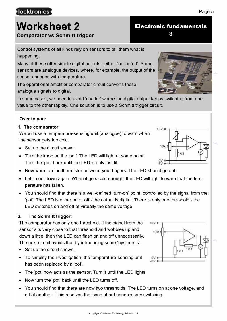
Worksheet 2 Comparator vs Schmitt trigger
Over to you:
1. The comparator:
We will use a temperature-sensing unit (analogue) to warn when
the sensor gets too cold.
Set up the circuit shown.
Turn the knob on the ‘pot’. The LED will light at some point.
Turn the ’pot’ back until the LED is only just lit.
Now warm up the thermistor between your fingers. The LED should go out.
Let it cool down again. When it gets cold enough, the LED will light to warn that the tem-
perature has fallen.
You should find that there is a well-defined ‘turn-on’ point, controlled by the signal from the
‘pot’. The LED is either on or off - the output is digital. There is only one threshold - the
LED switches on and off at virtually the same voltage.
2. The Schmitt trigger:
The comparator has only one threshold. If the signal from the
sensor sits very close to that threshold and wobbles up and
down a little, then the LED can flash on and off unnecessarily.
The next circuit avoids that by introducing some ‘hysteresis’.
Set up the circuit shown.
To simplify the investigation, the temperature-sensing unit
has been replaced by a ‘pot’.
The ‘pot’ now acts as the sensor. Turn it until the LED lights.
Now turn the ‘pot’ back until the LED turns off.
You should find that there are now two thresholds. The LED turns on at one voltage, and
off at another. This resolves the issue about unnecessary switching.
Control systems of all kinds rely on sensors to tell them what is
happening.
Many of these offer simple digital outputs - either ‘on’ or ‘off’. Some
sensors are analogue devices, where, for example, the output of the
sensor changes with temperature.
The operational amplifier comparator circuit converts these
analogue signals to digital.
In some cases, we need to avoid ‘chatter’ where the digital output keeps switching from one
value to the other rapidly. One solution is to use a Schmitt trigger circuit.
w2b
w2c
w2a

Electronic fundamentals
3
Page 6
Copyright 2010 Matrix Technology Solutions Ltd
Worksheet 2 Comparator vs Schmitt trigger
So what?
The comparator is the easier circuit to design and use.
The LED switches on and off at the same threshold
voltage, V2, set by the ‘pot’.
The temperature-sensing unit (TSU) consists of a
thermistor and a fixed resistor.
As the temperature falls, the thermistor resistance
rises, and so the TSU output voltage, V1, falls.
When V1 falls below the value of V2, the LED switches on.
(This result was obtained in worksheet 1.)
Near the switching threshold, any electrical noise could push the
signal over the threshold, and cause the output to switch rapidly on and off, from
the noise alone. Then, it may be better to use a Schmitt trigger circuit.
The behaviour of the op-amp is unchanged:
When V2 is bigger than V1, the LED is on.
When V1 is bigger than V2, the LED is off.
The output of the op-amp sits at either +Vsat, (positive
saturation ,) or -Vsat (negative saturation.)
The two equal (1k) resistors are connected in
series between the output and 0V and so each has a
voltage drop of ½Vsat across it. Hence V2 = ½Vsat .
For example, ideally the output of the op-amp should saturate at +6V and -6V. This means
that V2 is either +3V or -3V.
When the LED is off, the op-amp output is -6V, and V2 = -3V. The input signal, V1 must
fall below -3V to switch the LED on.
When the LED is on, the output of the op-amp is +6V, and V2 = +3V. The input signal,
V1 must rise above +3V to switch the LED off.
There are now two switching thresholds.
For your records:
Draw the circuit diagram to show a temperature-sensing unit connected to :
a comparator circuit;
a Schmitt trigger circuit. (You will have to modify the one given above!)
Write a clear explanation in no more than 50 words on the difference between comparators
and Schmitt triggers.
Design a Schmitt trigger circuit like the one above but which has switching thresholds of
+2V and -2V. Assume that the saturation voltages are +6V and -6V.
w2e
Temperature sensing
unit
w2d
Lights when V2 > V1
Sets the threshold
Lights when V2 > V1

Electronic fundamentals
3
Page 7
Copyright 2010 Matrix Technology Solutions Ltd
Worksheet 3 Non-inverting amplifier
Over to you:
This investigation uses the circuit shown opposite.
Build this, using a value of 1k for RF and 1k for R1.
Use a 10k ‘pot’ as the input device, as before.
Be careful to connect up the power supply correctly.
The +6V power rail is connected to the ‘pot’, and also
provides power to the op-amp, though this is not shown
in the circuit diagram. Similarly the -6V power rail is
connected to the ‘pot’, and also provides power to the op-amp.
Use a digital multimeter (DMM) set on the 20V DC range to
monitor the voltage VIN. Turn the ‘pot’ to set this voltage to
+2.5V.
Measure the output voltage VOUT and record its value in the
first row of the table.
Repeat this process for all the other values of VIN.
Calculate the gain using the formula:
Voltage gain = VOUT / VIN
Use your results to complete the third column.
Now swap the 1k feedback resistor for a 10k resistor.
Repeat the process outlined above, using the new values of
VIN given in the second table.
Complete the second table in the same way as before.
Avionic systems need careful design. It’s not enough to
design each stage as a separate system. Each stage must
‘talk’ effectively to the next, i.e. must transfer its signal
without loss or distortion.
The operational amplifier has a number of roles in this.
Designed properly, the non-inverting amplifier draws very
little current from the input subsystem that supplies it with a
signal, an important element of the design.
In this worksheet you investigate the gain of a non-inverting amplifier stage.
w3b
RF = 1k, R1 = 1k
VIN VOUT Gain
+2.5V
+1.5V
+0.5V
-0.5V
-1.5V
-2.5V
RF = 10k, R1 = 1k
VIN VOUT Gain
+0.5V
+0.3V
+0.1V
-0.1V
-0.3V
-0.5V
w3a
Electronic fundamentals
3
Page 8
Copyright 2010 Matrix Technology Solutions Ltd
Worksheet 3 Non-inverting amplifier
So what?
The industry standard op-amp is the ‘741’, produced by Fairchild Semiconductors in 1968.
Since then, many improvements have been made to the performance.
The ideal characteristics of an op-amp are:
infinite open-loop voltage gain;
infinite bandwidth, (the range of frequencies amplified successfully;)
infinite input impedance, (draws no current from the device creating its input signal;)
infinite slew-rate, (the output voltage can leap instantly to any value;)
zero output impedance, (delivers the full output voltage to any subsystem that follows;)
infinite common-mode rejection ratio (CMRR) (amplifies only the difference in voltage
between the inputs and ignores any voltage common to both, such as interference.)
Often, subsystems delivering a signal to an amplifier, such as a microphone, cannot provide
much current. If the amplifier draws significant current from it, then the signal voltage falls,
defeating the point of using an amplifier. The non-inverting amplifier, however, offers a very
high input impedance, typically 1M, so that it draws very little current from its signal source.
The theoretical value for the voltage gain is given by the formula:
Voltage gain = 1 + RF / R1
For the first part of the investigation, where RF = 1k and R1 = 1k, this gives a value:
Voltage gain = 1 + 1 / 1 = 2
(Using any two equal valued resistors would give the same voltage gain. Using high values
reduces battery drain and power dissipation.)
For the second part, where RF = 10k and R1 = 1k, this gives a value:
Voltage gain = 1 + 10 / 1 = 11.
Look at your measurements. Do they support these values of voltage gain?
Replace the ’pot’ with a signal generator, set to output sine waves with an amplitude of
100mV at a frequency of 1kHz. Use an oscilloscope to measure the amplitude of the input
and output signals, and hence measure the AC voltage gain.
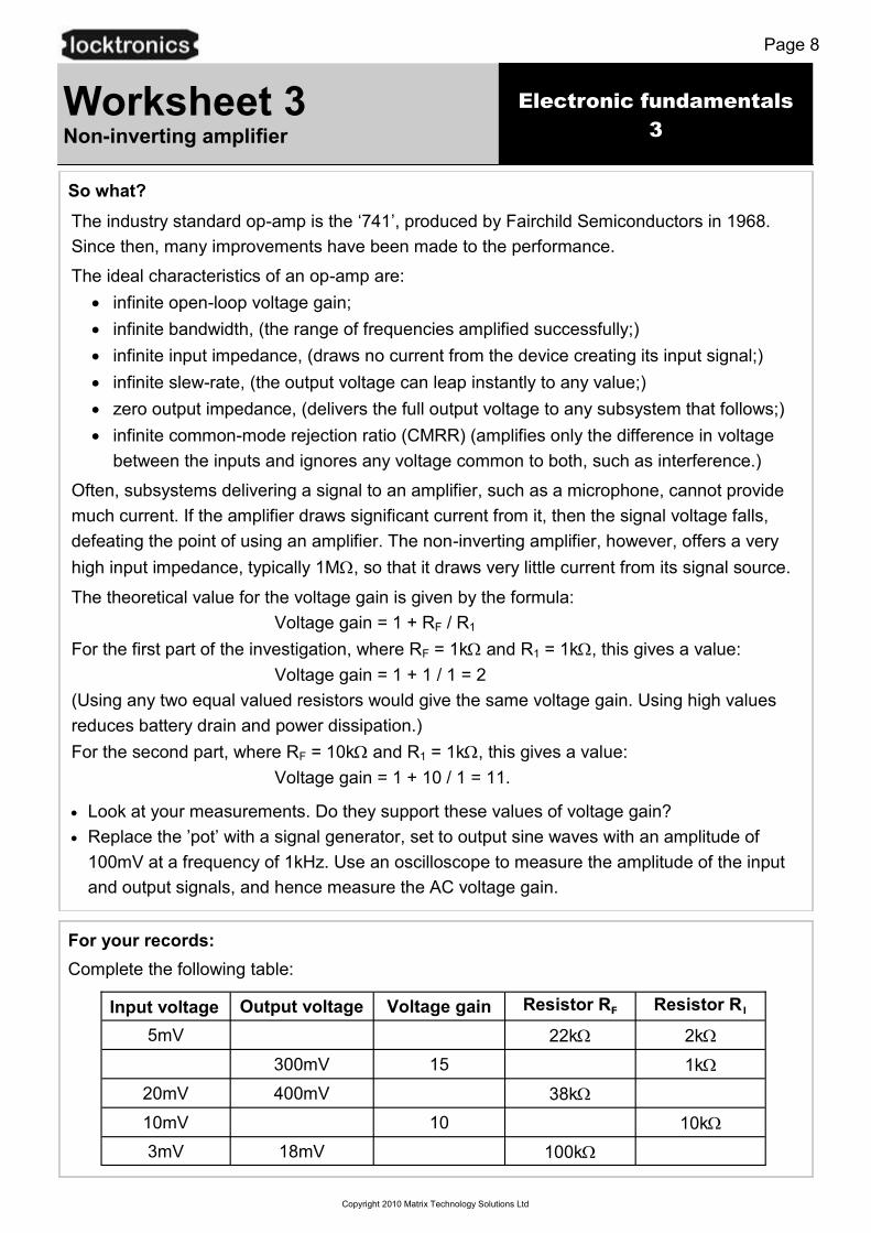
For your records:
Complete the following table:
Input voltage Output voltage Voltage gain Resistor RF Resistor R1
5mV 22k 2k
300mV 15 1k
20mV 400mV 38k
10mV 10 10k
3mV 18mV 100k
Electronic fundamentals
3
Page 9
Copyright 2010 Matrix Technology Solutions Ltd
Worksheet 4 Voltage follower
Over to you:
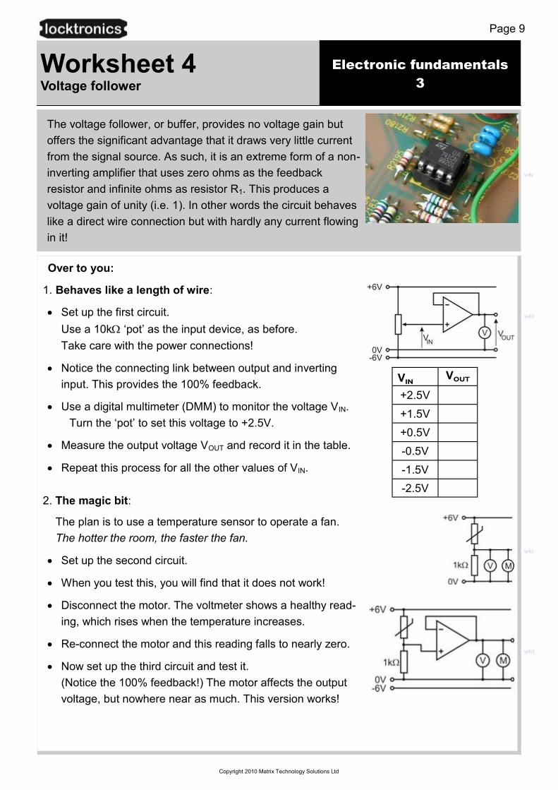
1. Behaves like a length of wire:
Set up the first circuit.
Use a 10k ‘pot’ as the input device, as before.
Take care with the power connections!
Notice the connecting link between output and inverting
input. This provides the 100% feedback.
Use a digital multimeter (DMM) to monitor the voltage VIN.
Turn the ‘pot’ to set this voltage to +2.5V.
Measure the output voltage VOUT and record it in the table.
Repeat this process for all the other values of VIN.
2. The magic bit:
The plan is to use a temperature sensor to operate a fan.
The hotter the room, the faster the fan.
Set up the second circuit.
When you test this, you will find that it does not work!
Disconnect the motor. The voltmeter shows a healthy read-
ing, which rises when the temperature increases.
Re-connect the motor and this reading falls to nearly zero.
Now set up the third circuit and test it.
(Notice the 100% feedback!) The motor affects the output
voltage, but nowhere near as much. This version works!
The voltage follower, or buffer, provides no voltage gain but
offers the significant advantage that it draws very little current
from the signal source. As such, it is an extreme form of a non-
inverting amplifier that uses zero ohms as the feedback
resistor and infinite ohms as resistor R1. This produces a
voltage gain of unity (i.e. 1). In other words the circuit behaves
like a direct wire connection but with hardly any current flowing
in it!
w4c
w4d
w4b
w4a
VIN VOUT
+2.5V
+1.5V
+0.5V
-0.5V
-1.5V
-2.5V
Electronic fundamentals
3
Page 10
Copyright 2010 Matrix Technology Solutions Ltd
Worksheet 4 Voltage follower
So what?
Matching for voltage transfer:
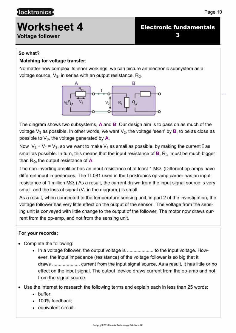
No matter how complex its inner workings, we can picture an electronic subsystem as a
voltage source, VS, in series with an output resistance, RO.
The diagram shows two subsystems, A and B. Our design aim is to pass on as much of the
voltage VS as possible. In other words, we want V2, the voltage ‘seen’ by B, to be as close as
possible to VS, the voltage generated by A.
Now V2 + V1 = VS, so we want to make V1 as small as possible, by making the current I as
small as possible. In turn, this means that the input resistance of B, RI, must be much bigger
than RO, the output resistance of A.
The non-inverting amplifier has an input resistance of at least 1 M. (Different op-amps have
different input impedances. The TL081 used in the Locktronics op-amp carrier has an input
resistance of 1 million M.) As a result, the current drawn from the input signal source is very
small, and the loss of signal (V1 in the diagram,) is small.
As a result, when connected to the temperature sensing unit, in part 2 of the investigation, the
voltage follower has very little effect on the output of the sensor. The voltage from the sens-
ing unit is conveyed with little change to the output of the follower. The motor now draws cur-
rent from the op-amp, and not from the sensing unit.
w4e
For your records:
Complete the following:
In a voltage follower, the output voltage is .................... to the input voltage. How-
ever, the input impedance (resistance) of the voltage follower is so big that it
draws ..................... current from the input signal source. As a result, it has little or no
effect on the input signal. The output device draws current from the op-amp and not
from the signal source.
Use the internet to research the following terms and explain each in less than 25 words:
buffer;
100% feedback;
equivalent circuit.

Electronic fundamentals
3
Page 11
Copyright 2010 Matrix Technology Solutions Ltd
Worksheet 5 Inverting amplifier
The inverting amplifier is somewhat inferior as a voltage
amplifier, but leads to a number of exciting applications
based on this circuit.
The fact that it inverts the signal is rarely significant - an
audio signal sounds just the same whether or not it is
inverted!
More importantly, the inverting amplifier usually draws
more current from its signal source, than does the non-
inverting amplifier, and so needs careful design.
Over to you:
The next investigation uses the circuit shown opposite.
Build this, using a value of 10k for RF and 10k for
RIN. Use a 10k ‘pot’ as the input device, as before.
Be careful to connect up the power supply correctly!
The +6V power rail is connected to the ‘pot’, and also
provides power to the op-amp. Similarly the -6V power
rail is connected to the ‘pot’, and to the op-amp.
Use a digital multimeter (DMM) to monitor the input voltage VIN.
Turn the ‘pot’ to set this to +2.5V.
Measure the output voltage VOUT and record it in the
first row of the table.
Repeat this process for all the other values of VIN.
Calculate the voltage gain using the formula:
Voltage gain = VOUT / VIN
and hence complete the third column.
Now swap the 10k input resistor for a 1k resistor.
Repeat the same process, using the values of VIN given in the
second table.
Complete the second table in the same way as before.
The formula for the voltage gain is simpler than for the non-
inverting amplifier. How could you use a 10k resistor and two
1k resistors to give you a voltage gain of 5?
Test your idea by modifying the circuit you used above.
w5a
w5b
RF = 10k, RIN = 10k
VIN VOUT Gain
+2.5V
+1.5V
+0.5V
-0.5V
-1.5V
-2.5V
RF = 10k, RIN = 1k
VIN VOUT Gain
+0.5V
+0.3V
+0.1V
-0.1V
-0.3V
-0.5V

Electronic fundamentals
3
Page 12
Copyright 2010 Matrix Technology Solutions Ltd
Worksheet 5 Inverting amplifier
So what?
A significant result :
V2 = V1
in any op-amp circuit where the output is not saturated.
The reason:
The output voltage is never very large, say 10V maximum.
Provided that the output is not saturated, VOUT = A0 x (V2 - V1).
Open loop gain, A0, is around 100,000.
Hence, 10 = 100,000 x (V2 - V1), so (V2 - V1) ~ 0.0001V, or, to a good approximation:
V2 = V1
In the case of the inverting amplifier, V2 = 0V, because it is connected directly to it.
As long as the output is not saturated, V1 = 0V also. This can be a good experimental check
that the op-amp is working correctly.
For the inverting amplifier:
Voltage gain = - RF / RIN
As a result:
when RF = RIN, the voltage gain = -1;
when RF = 10 x RIN, the voltage gain = -10, and so on.
However, because V1 = 0V when the output is not saturated, (and amplifi-
ers should never be driven into saturation,) the input source sees the am-
plifier as the input resistor connected to 0V, as the diagram shows.
The value of RIN should be kept large in order to limit the current that the amplifier draws from
the input source. It should be at least 1k, and preferably bigger than 10k.
Replace the ’pot’ with a signal generator, set to output sine waves with an amplitude of
100mV at a frequency of 1kHz. Use an oscilloscope to measure the amplitude of the input
and output signals, and hence measure the AC voltage gain.
For your records:
Complete following table :
w5c
w5d
Input voltage Output voltage Voltage gain Resistor RF Resistor RIN
5mV 20k 2k
-300mV 12 10k
20mV 100mV 100k
-10mV 3 10k
3mV -24mV 240k
Electronic fundamentals
3
Page 13
Copyright 2010 Matrix Technology Solutions Ltd
Worksheet 6 Summing amplifier
The inverting amplifier has only one input. However,
we can add other inputs in such a way that each op-
erates independently, with the result that the
output voltage is the sum of the individual inputs.
This allows us to combine signals from a number of
different transducers or signal sources.
In this worksheet you investigate a simple summing
amplifier with only two inputs.
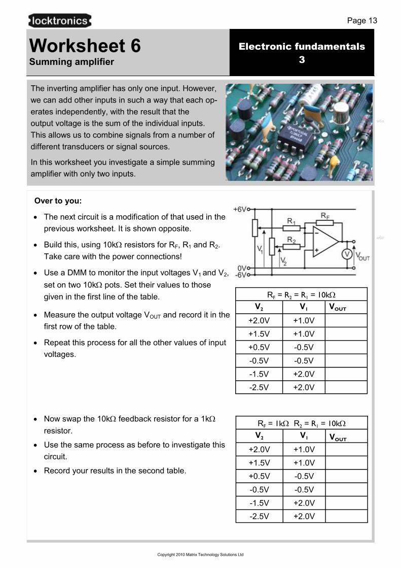
Over to you:
The next circuit is a modification of that used in the
previous worksheet. It is shown opposite.
Build this, using 10k resistors for RF, R1 and R2.
Take care with the power connections!
Use a DMM to monitor the input voltages V1 and V2,
set on two 10k pots. Set their values to those
given in the first line of the table.
Measure the output voltage VOUT and record it in the
first row of the table.
Repeat this process for all the other values of input
voltages.
Now swap the 10k feedback resistor for a 1k
resistor.
Use the same process as before to investigate this
circuit.
Record your results in the second table.
w6a
w6b
RF = R2 = R1 = 10k
V2 V1 VOUT
+2.0V +1.0V
+1.5V +1.0V
+0.5V -0.5V
-0.5V -0.5V
-1.5V +2.0V
-2.5V +2.0V
RF = 1k R2 = R1 = 10k
V2 V1 VOUT
+2.0V +1.0V
+1.5V +1.0V
+0.5V -0.5V
-0.5V -0.5V
-1.5V +2.0V
-2.5V +2.0V

Electronic fundamentals
3
Page 14
Copyright 2010 Matrix Technology Solutions Ltd
Worksheet 6 Summing amplifier
w5x
w5y
So what?
A significant result :
and when RF = R1 = R2 we have:
The minus sign results from the inverting amplifier.
Recall that for a simple inverting amplifier with only one input:
Voltage gain = - RF / RIN
F FOUT 1 2
1 2
R RV V V
R R
OUT 1 2V V V
For your records:
Complete the following table:
Input voltage
V1
Resistor R1
Input voltage V2
Resistor R2
Resistor RF
Output voltage VOUT
150 mV 2 k 350 mV 2k 10 k
100 k 1 V 50 k 100 k -1 V
200 mV 50 k 500 mV 100 k 100 k
-10 mV 2.5 k 2.5 k 10 k 0 V
300 mV 1 k -90 mV 1.2 k 150 mV

Electronic fundamentals
3
Page 15
Copyright 2010 Matrix Technology Solutions Ltd
Worksheet 7 Differential amplifiers
Most avionic op-amp applications are found in control and
instrumentation systems of one kind or another.
The differential amplifier has application to many of these
systems and its name gives a clue as to what it does.
Its importance lies in the ability to distinguish between
background components to a signal, such as temperature
and power supply voltage, and the true signal.
It is often used in conjunction with bridge circuits, to
monitor, for example, strain in aircraft structures, such as fuselages and wings.
Over to you:
The next circuit is another modification of the inverting
amplifier used earlier. It is shown opposite.
Build this, using two 10k resistors and two 1k resistors.
Use two 10k ‘pots’ to provide the input signals, VA and VB.
Notice the symmetry of the arrangement. The two input
resistors are equal. The inverting input is connected through
a 10k resistor to the output. The non-inverting input is
connected through a 10k resistor to 0V.
Use a DMM to monitor the input voltages VA and VB.
Set their values to those given in the first line of the table.
Measure the output voltage VOUT and record it in the
first row of the table.
Repeat this process for all the other values of input voltages.
As with all amplifier circuits, it is important to avoid output
saturation. Watch out for this in your results!
Analyse your results.
Can you see the pattern that links VOUT to VA and VB?
Test your theories by trying other combinations of input voltages, and predicting the result.
w7a
w7b
VB VA VOUT
+2.0V +1.8V
+1.5V +1.2V
+0.4V 0V
0V -0.2V
-1.5V -1.3V
-2.2V -2.6V

Electronic fundamentals
3
Page 16
Copyright 2010 Matrix Technology Solutions Ltd
Worksheet 7 Differential amplifiers
For your records:
Calculate the output voltage if all four resistors in the circuit have a resistance of 10kΩ and the
input voltages are:
VA = +6V VB = +4V
Show how you obtain your answer.
So what?
Here is an analysis of the performance of the differential amplifier.
(The values of the resistors have been changed to make the arithmetic easier.)
Earlier we pointed out that the ideal op-amp has infinite input impedance, and so draws no
current from its input source. We will assume that the op-amp used here is ideal!
Look at point X, the non-inverting input of the op-amp. It is at the centre of a voltage divider.
We can draw it as shown opposite:
There is a 3V drop across two resistors, one of which is twice as big as the other.
As a result, the 2k resistor takes twice as much of the voltage as does the 1k re-
sistor, giving 2V across the 2k resistor and 1V across the 1k resistor.
In other words, point X sits at 2V.
Assuming that the output of the op-amp is not saturated, the two inputs must sit at
the same voltage (as we pointed out earlier.) In other words, point Y sits at 2V too.
The output of the op-amp can be viewed as part of a voltage divider. The 1k input
resistor has a 2V drop across it (from 4V at the input to 2V at point Y.) The 2k
resistor in series with it must have twice as big a voltage drop, i.e. 4V.
Looking at the blue current arrows on the diagram, current flows from point Y to the
output. That means that the output is at a lower voltage than point Y, in this case 4V
lower. As Y is at 2V, the output must be at (2 - 4) = -2V.
w7c
w7d
w7e
Electronic fundamentals
3
Page 17
Copyright 2010 Matrix Technology Solutions Ltd
A differentiator produces an output voltage that represents
the rate of change of its input. This simply means that, if
the input voltage remains constant (i.e. isn’t changing,) the
output voltage also remains constant.
If the input voltage changes, the output voltage takes a
value that is proportional to the rate at which the input is
changing. The faster the input voltage changes, the greater
will be the output ,
In mathematics this is equivalent to the differential function.
In this worksheet, you investigate the an operational
amplifier differentiator, supplied with a square wave input. This waveform is used because the
steeply rising and falling edges exhibit a very rapid rate of change whilst the mark and space,
(top and bottom) are ‘flat’ and so have zero rate of change.
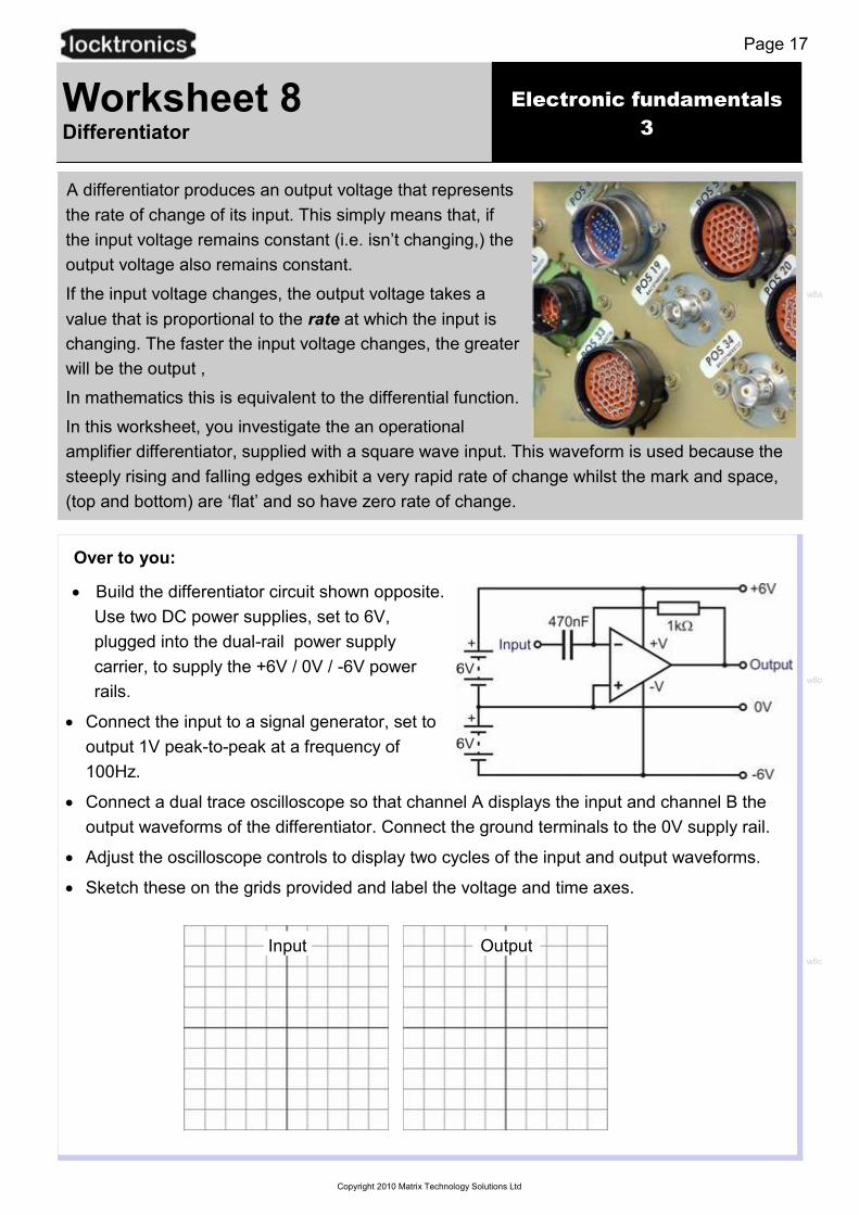
Worksheet 8 Differentiator
Over to you:
Build the differentiator circuit shown opposite.
Use two DC power supplies, set to 6V,
plugged into the dual-rail power supply
carrier, to supply the +6V / 0V / -6V power
rails.
Connect the input to a signal generator, set to
output 1V peak-to-peak at a frequency of
100Hz.
Connect a dual trace oscilloscope so that channel A displays the input and channel B the
output waveforms of the differentiator. Connect the ground terminals to the 0V supply rail.
Adjust the oscilloscope controls to display two cycles of the input and output waveforms.
Sketch these on the grids provided and label the voltage and time axes.
w8a
w8b
w8c
Input Output

Electronic fundamentals
3
Page 18
Copyright 2010 Matrix Technology Solutions Ltd
So what?
A typical set of waveforms is shown in the picture.
A significant point!
Notice that the negative going ‘spikes’ on the output waveform occur on the fast rising edge
of the square waveform whereas the positive going ‘spikes’ occur on the fast falling edge of
the square waveform.
The output of the differentiator is thus the inverse of the differential of its input function.
Expressed in mathematical terms the output voltage is given by:
In other words the output is the derivative function of the input.
The performance of the differentiator (and its ability to produce an accurate differential
function) is determined primarily by the ratio of the time constant of the RC network to the
periodic time of the input function.
For accurate differentiation the periodic time, t, needs to be very much larger than the time
constant, RC (typically at least ten times larger).
Calculate the ratio of t to RC used in this circuit:
Worksheet 8 Differentiators
INOUT
d(V )V
dt
tRatio,
CR
w8d
For your records:
Investigate what happens when you change the type of input signal. For example, input a
100Hz sine wave, and, if your signal generator provides it, a 100Hz triangular wave.
Electronic fundamentals
3
Page 19
Copyright 2010 Matrix Technology Solutions Ltd
An integrator provides the opposite function to that of
a differentiator.
Its output is equivalent to the area under the graph of
the input function rather than its rate of change.
If the input remains constant (and is other than 0V,)
the output voltage will ramp up or down according to
the polarity of the input.
The longer the input voltage remains at a particular
value, the larger the output voltage.
In this worksheet, you investigate the an operational
amplifier integrator, supplied with a square wave input.
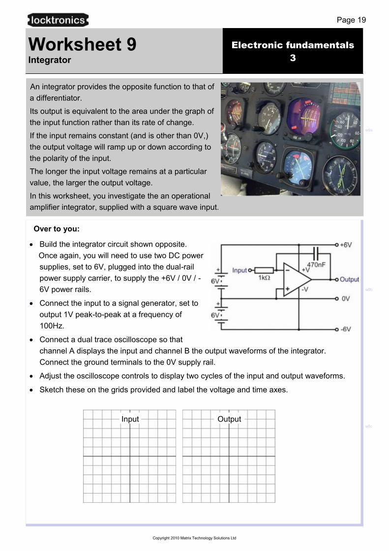
Worksheet 9 Integrator
Over to you:
Build the integrator circuit shown opposite.
Once again, you will need to use two DC power
supplies, set to 6V, plugged into the dual-rail
power supply carrier, to supply the +6V / 0V / -
6V power rails.
Connect the input to a signal generator, set to
output 1V peak-to-peak at a frequency of
100Hz.
Connect a dual trace oscilloscope so that
channel A displays the input and channel B the output waveforms of the integrator.
Connect the ground terminals to the 0V supply rail.
Adjust the oscilloscope controls to display two cycles of the input and output waveforms.
Sketch these on the grids provided and label the voltage and time axes.
w9a
w9b
w8c
Input Output
Electronic fundamentals
3
Page 20
Copyright 2010 Matrix Technology Solutions Ltd
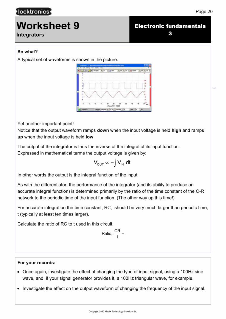
So what?
A typical set of waveforms is shown in the picture.
Yet another important point!
Notice that the output waveform ramps down when the input voltage is held high and ramps
up when the input voltage is held low.
The output of the integrator is thus the inverse of the integral of its input function.
Expressed in mathematical terms the output voltage is given by:
In other words the output is the integral function of the input.
As with the differentiator, the performance of the integrator (and its ability to produce an
accurate integral function) is determined primarily by the ratio of the time constant of the C-R
network to the periodic time of the input function. (The other way up this time!)
For accurate integration the time constant, RC, should be very much larger than periodic time,
t (typically at least ten times larger).
Calculate the ratio of RC to t used in this circuit.
Worksheet 9 Integrators
w9c
OUT INV V dt
CRRatio,
t
For your records:
Once again, investigate the effect of changing the type of input signal, using a 100Hz sine
wave, and, if your signal generator provides it, a 100Hz triangular wave, for example.
Investigate the effect on the output waveform of changing the frequency of the input signal.

Electronic fundamentals
3
Page 21
Copyright 2010 Matrix Technology Solutions Ltd
Worksheet 10 Logic gates
Logic gates are one of the commonest digital integrated circuits. They perform logic functions,
such as NOT, AND and OR. This worksheet looks at the simplest of these, the NOT function.
This could be used to warn when an undercarriage door is NOT closed, for example.
Logic gates can be built in a variety of ways, resulting in a number of logic ‘families,’ each with
its own capabilities and limitations. One of these is called CMOS.
The photograph shows a CMOS NOT gate, identified by ‘4049’. It is
known as a ‘hex inverting buffer.’ (Hex = 6, inverting =
NOT, buffer = able to deliver a ~ milliamps of current)
meaning that the IC has six NOT gates, each with some
current capability.
Like all electronic devices, logic gates are represented by circuit
symbols, but there several versions of them. The common ones are
‘ANSI’ (American National Standards Institute) and ‘BS’ (British
Standard) also called ‘SB’ (System Block) symbols. Both are given in
the diagram opposite but aircraft schematics invariably use the ANSI
symbols.
w10b
Over to you:
Build the circuit shown opposite. Notice the LED connected
between the output of the NOT gate and 0V. This is in addition to
the LED built into the NOT gate carrier itself.
Set the DC power supply to 6V.
With the multimeter on the 20V DC range, measure the voltages at
the input and then output of the NOT gate when the switch is
turned off (open.)
Record both readings in the first table.
Note whether the external LED is on or off.
Now close the switch, and repeat the
measurements. Record them in the first table.
Invert the switch unit, by swapping over the
switch and 10k resistor. Repeat the
measurements and record them in the
second table.
w10c
w10a
Switch unit
Input voltage
Output voltage
State of LED
Open (off)
Closed (on)
Switch unit inverted
Input voltage
Output voltage
State of LED
Open (off)
Closed (on)

Electronic fundamentals
3
Page 22
Copyright 2010 Matrix Technology Solutions Ltd
Worksheet 10 Logic gates
So what?
First, a word about logic levels. The voltages you measured are either pretty close to +6V or
0V. For CMOS logic gates, logic 1 is any voltage greater than 70% of the supply voltage, and
logic 0 anything less than 30% of supply voltage. In this case, with a 6V power supply, logic 1
is bigger than 4.2V and logic 0 is less than 1.8V.
Use this information to convert your input and output voltage
readings into logic levels. Complete the table, known as the truth-
table, for the NOT gate, which describes the behaviour of the gate.
The NOT gate produced the same effect, whether the switch unit was
inverted or not. It turned a logic 0 input into a logic 1 output, and vice-versa. The behaviour of
the switch unit changed. To begin with, it produced a logic 0 signal when the switch was open,
and a logic 1 signal when closed. When inverted, the behaviour inverted so that with the
switch open, it generated a logic 1 signal and, with it closed logic 0.
A challenge - Why do we need a resistor in the switch unit? Why not just have the switch?
See what happens when you remove the resistor from the switch unit.
With the switch between the +6V supply and the input, things seem to behave as before,
when the resistor was in place. However, with the switch connected between the input and the
0V connection, nothing happens. The output of the NOT gate always sits at logic 1,
regardless of the state of the switch.
CMOS circuitry is wonderful, but it has a weakness - the inputs must not ‘float’ (be left
unconnected). If they are, the outcome is unpredictable. The output can even oscillate so
rapidly between logic 0 and logic 1, that the circuit can overheat and be destroyed. Always
use a resistor either to ‘pull’ the input up to logic 1, by connecting it between the positive
supply and the input, or ‘pull’ it down to logic 0, by connecting it between the input and 0V.
The ‘Locktronics’ NOT gate carrier is wired up so that the input sits at logic 0, when
nothing is connected to it.
NOT gate
Input Output
(Logic) 0
(Logic) 1
For your records:
A surprise - we said that a CMOS NOT gate carries the serial number ‘4049’. Remove the
NOT gate carrier, turn it upside down and look at the integrated circuit used in it. The serial
number on it is ‘4011’. Find out what the ‘4011’ chip is.
Another challenge - What happens if you connect the output of one NOT gate to the input
of another NOT gate? How does the output of the second NOT gate relate to the input of
the first NOT gate? Is this what you would expect?
Electronic fundamentals
3
Page 23
Copyright 2010 Matrix Technology Solutions Ltd
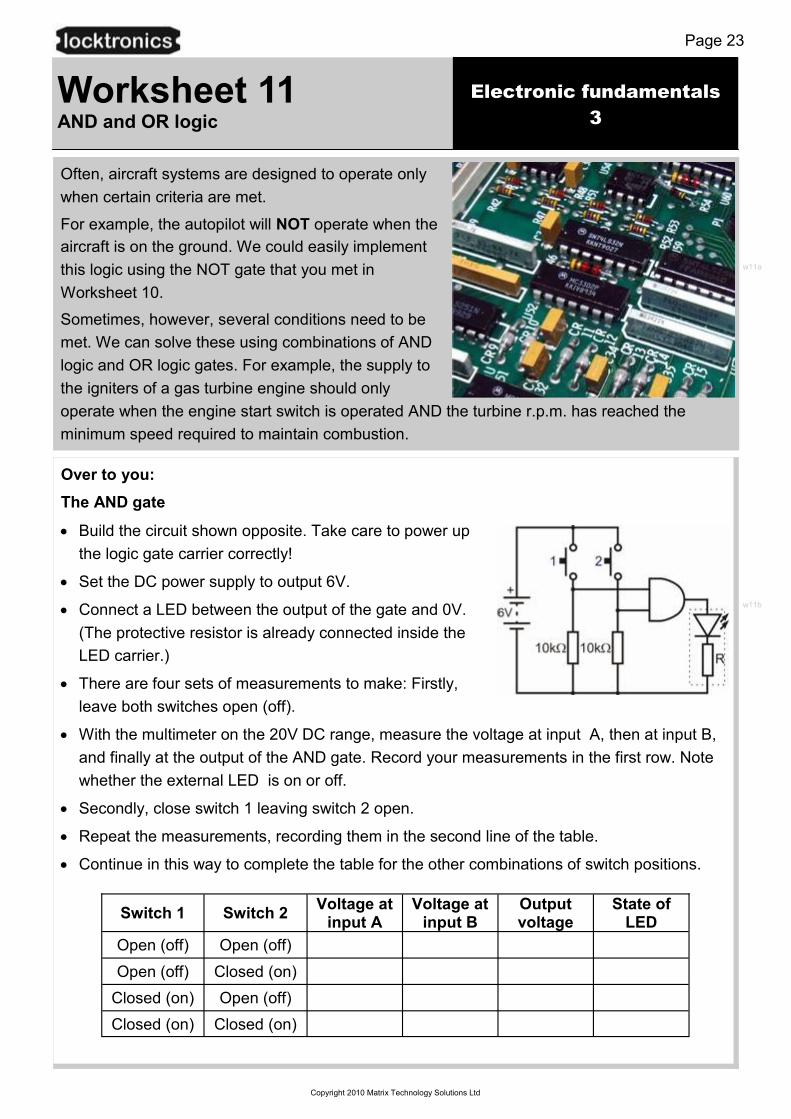
Worksheet 11 AND and OR logic
Over to you:
The AND gate
Build the circuit shown opposite. Take care to power up
the logic gate carrier correctly!
Set the DC power supply to output 6V.
Connect a LED between the output of the gate and 0V.
(The protective resistor is already connected inside the
LED carrier.)
There are four sets of measurements to make: Firstly,
leave both switches open (off).
With the multimeter on the 20V DC range, measure the voltage at input A, then at input B,
and finally at the output of the AND gate. Record your measurements in the first row. Note
whether the external LED is on or off.
Secondly, close switch 1 leaving switch 2 open.
Repeat the measurements, recording them in the second line of the table.
Continue in this way to complete the table for the other combinations of switch positions.
Often, aircraft systems are designed to operate only
when certain criteria are met.
For example, the autopilot will NOT operate when the
aircraft is on the ground. We could easily implement
this logic using the NOT gate that you met in
Worksheet 10.
Sometimes, however, several conditions need to be
met. We can solve these using combinations of AND
logic and OR logic gates. For example, the supply to
the igniters of a gas turbine engine should only
operate when the engine start switch is operated AND the turbine r.p.m. has reached the
minimum speed required to maintain combustion.
w11a
w11b
Switch 1 Switch 2 Voltage at
input A Voltage at
input B Output voltage
State of LED
Open (off) Open (off)
Open (off) Closed (on)
Closed (on) Open (off)
Closed (on) Closed (on)

Electronic fundamentals
3
Page 24
Copyright 2010 Matrix Technology Solutions Ltd
Worksheet 11 AND and OR logic
Over to you:
The OR gate
Build the circuit shown opposite, with the DC power
supply set to output 6V.
Connect the LED carrier between the output of the OR
gate and 0V.
Follow the same steps as for the AND gate, recording
your results in the table.
Switch 1 Switch 2
Voltage at input A
Voltage at input B
Output voltage
State of LED
Open (off) Open (off)
Open (off) Closed (on)
Closed (on) Open (off)
Closed (on) Closed (on)
w11c
So what?
As before, you used a 6V power supply and so logic 1 is any voltage greater than 4.2V and
logic 0 is any voltage less than 1.8V. Use this and your measurements to complete the truth-
table for the two types of gate.
The AND and OR logic functions are easy to understand. The output of the AND gate will be
logic 1 only when input A AND input B (AND input C etc. if there are more inputs), are all logic
1. The output of the OR gate will be logic 1 when either input A OR input B (or both!) inputs are
at logic 1. Your results should confirm this behaviour.
Input A Input B AND
0 0
0 1
1 0
1 1
Input A Input B OR
0 0
0 1
1 0
1 1
For your records:
Work out what happens in the following circuit, and fill in the
truth table:
Confirm your ideas by building and testing the logic system.
w11d
A B C D Q
0 0
0 1
1 0
1 1

Electronic fundamentals
3
Page 25
Copyright 2010 Matrix Technology Solutions Ltd
Questions
About these questions
These questions are typical of those that you will be required to answer in the EASA Part-66
examination.
You should allow 15 minutes to answer these questions and then check your answers with
those given on page 36.
Please remember that ALL these questions must be attempted without the use of a calculator
and that the pass mark for all Part-66 multiple-choice examinations is 75%!
1. The connection marked ‘X’ in the diagram is the:
(a) inverting input
(b) non-inverting input
(c) positive supply input.
2. The typical value of open-loop voltage gain for an operational amplifier is:
(a) between 10 and 100
(b) between 100 and 1000
(c) more than 100,000.
3. In normal operation, the output voltage of a comparator will be at a voltage which is:
(a) close to zero
(b) close to either the positive or negative supply voltage
(c) the same as the input voltage.
4. Operational amplifiers have:
(a) very high input resistance and very high open-loop voltage gain
(b) very high input resistance and very low open-loop voltage gain
(c) very low input resistance and very high open-loop voltage gain.
5. The input resistance of an operational amplifier is typically:
(a) less than 100 Ω
(b) between 1 kΩ and 10 kΩ
(c) more than 1 MΩ.
6. Which of the logic gates shown have inverted outputs?
(a) A and B
(b) B and D
(c) C and D
7. The output resistance of an operational amplifier is typically:
(a) less than 100 Ω
(b) between 1 kΩ and 10 kΩ
(c) more than 1 MΩ.
rq1
rq2
Electronic fundamentals
3
Page 26
Copyright 2010 Matrix Technology Solutions Ltd
Questions
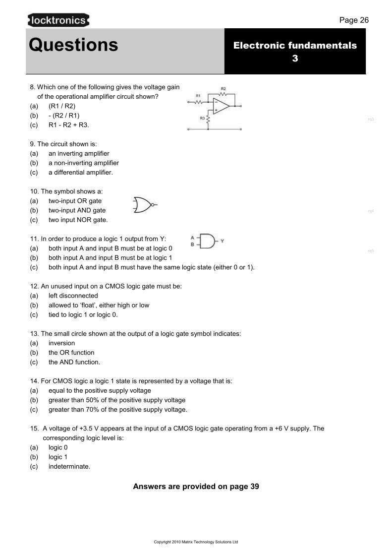
8. Which one of the following gives the voltage gain
of the operational amplifier circuit shown?
(a) (R1 / R2)
(b) - (R2 / R1)
(c) R1 - R2 + R3.
9. The circuit shown is:
(a) an inverting amplifier
(b) a non-inverting amplifier
(c) a differential amplifier.
10. The symbol shows a:
(a) two-input OR gate
(b) two-input AND gate
(c) two input NOR gate.
11. In order to produce a logic 1 output from Y:
(a) both input A and input B must be at logic 0
(b) both input A and input B must be at logic 1
(c) both input A and input B must have the same logic state (either 0 or 1).
12. An unused input on a CMOS logic gate must be:
(a) left disconnected
(b) allowed to ‘float’, either high or low
(c) tied to logic 1 or logic 0.
13. The small circle shown at the output of a logic gate symbol indicates:
(a) inversion
(b) the OR function
(c) the AND function.
14. For CMOS logic a logic 1 state is represented by a voltage that is:
(a) equal to the positive supply voltage
(b) greater than 50% of the positive supply voltage
(c) greater than 70% of the positive supply voltage.
15. A voltage of +3.5 V appears at the input of a CMOS logic gate operating from a +6 V supply. The
corresponding logic level is:
(a) logic 0
(b) logic 1
(c) indeterminate.
Answers are provided on page 39
rq3
rq4
rq5

Electronic fundamentals
3
Page 27
Copyright 2010 Matrix Technology Solutions Ltd
Learning Objectives
On successful completion of this course the student will have learned to:
recall the basic properties and characteristics of operational amplifiers;
describe the meaning and significance of output saturation;
explain the significance of the term ‘high gain differential voltage amplifier’;
distinguish between the performance of a comparator and a Schmitt trigger circuit;
draw the circuit diagram for a sensing unit connected to a comparator;
draw the circuit diagram for a sensing unit connected to a Schmitt trigger;
analyse the behaviour of an inverting Schmitt trigger;
identify the op-amp non-inverting amplifier circuit;
recall and use the formula for the voltage gain of an op-amp non-inverting amplifier;
measure the voltage gain of op-amp voltage amplifiers;
describe and explain the use of op-amp voltage followers;
identify the op-amp summing amplifier circuit;
recall and use the formula for the voltage gain of an op-amp summing amplifier;
identify the op-amp diffference amplifier circuit;
calculate the output voltage of a given op-amp difference amplifier;
identify the op-amp differentiator circuit;
recall the significance of time constant to the performance of the differentiator circuit;
sketch of output waveform expected from the differentiator for a given input waveform;
identify the op-amp integrator circuit;
sketch of output waveform expected from the integrator for a given input waveform;
recall the basic properties and characteristics of AND, OR and NOT logic gates;
identify logic levels in relation to the supply voltages for CMOS logic circuits;
explain the logical operation of NOT, AND, and OR logic gates.
Tutor’s notes
About this course
Introduction
This workbook is intended to reinforce the learning that takes place in the classroom or lecture room. It
provides a series of practical activities and investigations that complement syllabus section 4.1.3 of
EASA Part-66 Module 4, Electronic Fundamentals.
Locktronics equipment makes it simple and quick to construct and investigate electrical circuits. The
end result can look exactly like the circuit diagram, thanks to the symbols printed on each component
carrier.
Aim
The workbook aims to introduce students to the basic underpinning principles and concepts of aircraft
electrical and electronic equipment. It also provides a useful introduction to electrical measurements
and the use of ammeters, voltmeters and oscilloscopes.
Prior Knowledge
Students should have previously studied (or should be concurrently studying) EASA Module 3
(Electrical Fundamentals) or should have equivalent knowledge at Level 3.

Electronic fundamentals
3
Page 28
Copyright 2010 Matrix Technology Solutions Ltd
Power sources:
Students will need to make use of an adjustable low-voltage DC supply.
The output voltage from the supplied DC power unit can be adjusted to
provide outputs of either 3 V, 4.5 V, 6 V, 7.5 V, 9 V or 13.5 V, with
currents typically up to 1 A. The voltage is changed by turning the
selector dial just above the earth pin until the arrow points to the
required voltage.
Tutors may decide to make any adjustment necessary to the power
supply voltage, or may allow students to make those changes.
Each exercise includes a recommended voltage for that particular
circuit.
In the example opposite, the DC power supply has been adjusted to provide
an output of 13.5 V DC.
Tutor’s notes
p28a
p28b
What students will need:
This pack is designed to work with the Locktronics Aircraft Maintenance Kit. The electrical / electronic parts required for this workbook are listed on the next page.
Students will also need:
either two multimeters, such as the LK1110, capable of measuring currents in the range 0 to 200mA,
and voltages in the range 0 to 200V;
or equivalent ammeters and voltmeters.
For other modules in the series, they will need:
a function generator, such as the LK8990, or equivalent;
and an oscilloscope capable of monitoring the signals it produces, such as the LK6730 Pico 4000
virtual oscilloscope.
If you are missing any components, or need additional items, please contact Matrix or your local dealer.
Electronic fundamentals
3
Page 29
Copyright 2010 Matrix Technology Solutions Ltd
Tutor’s notes
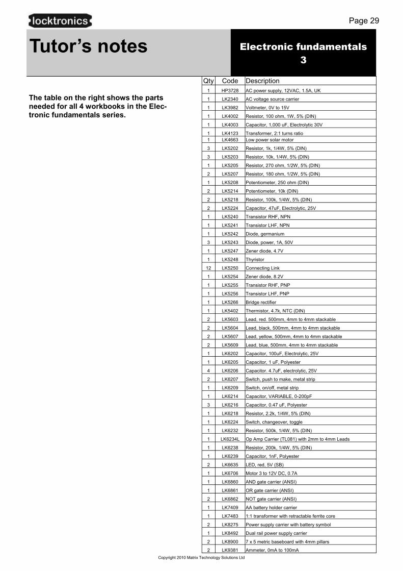
The table on the right shows the parts needed for all 4 workbooks in the Elec-tronic fundamentals series.
Qty Code Description
1 HP3728 AC power supply, 12VAC, 1.5A, UK
1 LK2340 AC voltage source carrier
1 LK3982 Voltmeter, 0V to 15V
1 LK4002 Resistor, 100 ohm, 1W, 5% (DIN)
1 LK4003 Capacitor, 1,000 uF, Electrolytic 30V
1 LK4123 Transformer, 2:1 turns ratio
1 LK4663 Low power solar motor
3 LK5202 Resistor, 1k, 1/4W, 5% (DIN)
3 LK5203 Resistor, 10k, 1/4W, 5% (DIN)
1 LK5205 Resistor, 270 ohm, 1/2W, 5% (DIN)
2 LK5207 Resistor, 180 ohm, 1/2W, 5% (DIN)
1 LK5208 Potentiometer, 250 ohm (DIN)
2 LK5214 Potentiometer, 10k (DIN)
2 LK5218 Resistor, 100k, 1/4W, 5% (DIN)
2 LK5224 Capacitor, 47uF, Electrolytic, 25V
1 LK5240 Transistor RHF, NPN
1 LK5241 Transistor LHF, NPN
1 LK5242 Diode, germanium
3 LK5243 Diode, power, 1A, 50V
1 LK5247 Zener diode, 4.7V
1 LK5248 Thyristor
12 LK5250 Connecting Link
1 LK5254 Zener diode, 8.2V
1 LK5255 Transistor RHF, PNP
1 LK5256 Transistor LHF, PNP
1 LK5266 Bridge rectifier
1 LK5402 Thermistor, 4.7k, NTC (DIN)
2 LK5603 Lead, red. 500mm, 4mm to 4mm stackable
2 LK5604 Lead, black, 500mm, 4mm to 4mm stackable
2 LK5607 Lead, yellow, 500mm, 4mm to 4mm stackable
2 LK5609 Lead, blue, 500mm, 4mm to 4mm stackable
1 LK6202 Capacitor, 100uF, Electrolytic, 25V
1 LK6205 Capacitor, 1 uF, Polyester
4 LK6206 Capacitor. 4.7uF, electrolytic, 25V
2 LK6207 Switch, push to make, metal strip
1 LK6209 Switch, on/off, metal strip
1 LK6214 Capacitor, VARIABLE, 0-200pF
3 LK6216 Capacitor, 0.47 uF, Polyester
1 LK6218 Resistor, 2.2k, 1/4W, 5% (DIN)
1 LK6224 Switch, changeover, toggle
1 LK6232 Resistor, 500k, 1/4W, 5% (DIN)
1 LK6234L Op Amp Carrier (TL081) with 2mm to 4mm Leads
1 LK6238 Resistor, 200k, 1/4W, 5% (DIN)
1 LK6239 Capacitor, 1nF, Polyester
2 LK6635 LED, red, 5V (SB)
1 LK6706 Motor 3 to 12V DC, 0.7A
1 LK6860 AND gate carrier (ANSI)
1 LK6861 OR gate carrier (ANSI)
2 LK6862 NOT gate carrier (ANSI)
1 LK7409 AA battery holder carrier
1 LK7483 1:1 transformer with retractable ferrite core
2 LK8275 Power supply carrier with battery symbol
1 LK8492 Dual rail power supply carrier
2 LK8900 7 x 5 metric baseboard with 4mm pillars
2 LK9381 Ammeter, 0mA to 100mA

Electronic fundamentals
3
Page 30
Copyright 2010 Matrix Technology Solutions Ltd
Tutor’s notes
Using this course:
It is expected that the worksheets are printed / photocopied, preferably in colour, for the
students’ use. Students should retain their own copy of the entire workbook.
Worksheets usually contain:
an introduction to the topic under investigation and its aircraft application;
step-by-step instructions for the practical investigation that follows;
a section headed ‘So What?’ which aims both to challenge learners by questioning their
understanding of a topic and also provides a useful summary of what has been learned.
It can be used to develop ideas and as a trigger for class discussion.
a section headed ‘Questions’ which provides further work for students to carry out.
Answers to these questions are provided at the end of this workbook.
This format encourages self-study, with students working at a rate that suits their ability. It is
for the tutor to monitor that students’ understanding is keeping pace with their progress
through the worksheets and to provide additional work that will challenge brighter learners.
One way to do this is to ‘sign off’ each worksheet, as a student completes it, and in the
process have a brief chat with each learner to assess their grasp of the ideas involved in the
exercises that it contains.
Finally, a set of examination ’Revision Questions’ has been provided to conclude the work on
each topic. These questions are of mixed difficulty and are typical of those that students will
face when they sit their Module 4 CAA examinations. It is recommended that students should
attempt these questions under examination conditions and without the use of notes or
calculators.
Time:
It will take most students between eight and ten hours to complete the full set of worksheets. It
is expected that a similar length of time will be needed to support the learning in a class,
tutorial or self-study environment.
Electronic fundamentals
3
Page 31
Copyright 2010 Matrix Technology Solutions Ltd
Tutor’s notes
Worksheet Notes for the Tutor Timing
1
The first issue is to familiarise students with the pinout of the op-amp, and to explain the significance of the ‘inverting’ and ‘non-inverting inputs. At this stage, no attempt is made to introduce the offset null connections.
The op-amp carrier uses a LM10 op-amp, which is based on the industry-standard ‘741’ but with vastly improved characteristics, especially input impedance. The students will meet this concept later in the course. For now, they may need to have the idea of a dual-rail power supply explained to them. The physical reality is that there is no such thing as 0V in this circuit. Although the power rails are labelled +6V / 0V / -6V, that is simply to conform to convention. They could equally well be labelled 12V / 6V / 0V. However, the convention is that voltages are measured from the centre voltage, and this is called 0V.
The aim of the first part of the investigation is merely to show that the output switches rapidly from one extreme (saturation voltage) to the other as the input voltage changes relative to the reference voltage set by the two equal resistors. The second stage measures the input voltages to investigate more closely this changeover. Students should be able to use a digital multimeter to measure voltage, though the instructor may have to remind them how to do this. Finally, the student swaps over the inputs to see the effect.
The ‘So what?’ section explains the significance of the description ‘high gain differential voltage amplifier’ and gives the formulae for voltage gain and for the basic behaviour of the op-amp. At this stage, there is no mention of feedback. The role of this circuit as a voltage comparator is described, but this may need to be driven home through a number of examples.
30 - 45 minutes
2
In Worksheet 1, students met the comparator. In this worksheet, they attach a temperature-sensing unit to one of the inputs, and a variable reference voltage, provided by a ‘pot’, to the other.
Although students should know the difference between a variable resistor and a potentiometer, they may need the instructor’s help to set up the
‘pot’. In particular, the instructor should check that the 10k resistor, and not the ’shorted’ output, is connected between the power supply rails. A simple rule is that resistors have two ‘legs’ and so do variable resistors. The ’pot’ uses all three legs. The secret of success is to adjust the ‘pot’ so that the LED is about to turn off. The slightest change to the temperature of the thermistor should then make that change happen.
The investigation then turns to the Schmitt trigger circuit. The aim is that students realise that the single switching threshold of the comparator can cause problems when the output of the sensor is subject to high levels of electrical noise, or any other factor that causes the output voltage to ‘wobble’. When near the switching threshold, this variation may be enough to make the output switch rapidly from one saturation value to the other. This ‘hunting’ can have serious consequences for the device attached to the output of the comparator, or to the comparator itself, as current demand rises sharply when switching takes place.
30 - 45 minutes
Electronic fundamentals
3
Page 32
Copyright 2010 Matrix Technology Solutions Ltd
Tutor’s notes
Worksheet Notes for the Tutor Timing
2
continued...
The Schmitt trigger overcomes this problem by having two switching thresholds. The output switches from negative to positive saturation at a low voltage, but stays there even if the voltage rises slightly (i.e. no hunting.) The output changes back only if the input rises to a relatively high voltage, (but then stays there even if the input fluctuates.) The circuit studied is known as an inverting Schmitt trigger. There is a non-inverting Schmitt trigger, but its analysis is a bit more complicated. Able students could be given the task of researching that circuit.
3
Now the students meet feedback. The instructor might wish to expand on the ideas of positive and negative feedback, as both are used in this module. Negative feedback always produces a calming effect on the circuit. It makes the output less likely to saturate. It reduces the huge open-loop voltage gain of the op-amp to a more manageable level. The idea of an amplifier is that the output follows the input, but is a larger version of it. If the output saturates, it can no longer follow changes in the input. Amplifiers use negative feedback, as their outputs should never saturate. Positive feedback, on the other hand, drives the output into saturation more readily, making it unlikely that the output is ever out of saturation. It is used in oscillators and Schmitt triggers, where the output is required to be in one value of saturation all the time.
While amplifiers are usually associated with audio systems, it makes sense to begin the investigation by using DC signals. These are easier to visualise and, probably, to measure. As students will discover in worksheet 5, these amplifiers have the same behaviour for DC and for low frequency AC signals.
The voltage gain of the amplifier is determined solely by the value of the two resistors, RF and R1, provided extreme values of gain or bandwidth are avoided. This investigation looks at two pairs of resistor values, to give gains of 2x and 11x. The instructor may wish to add other values, or vary the values between different groups and then later collate results.
Students often confuse the voltage gain formula (= VOUT / VIN) and the voltage gain formula showing the dependence on resistor values (= 1 + RF/R1.) Instructors should provide a range of examples to reinforce the significance of these formulae.
The analysis in ‘So what?’ introduces the ideal characteristics of op-amps. These will need a deal of reinforcement by the instructor, as some are fairly esoteric concepts. The important idea in there is the input impedance. As we are dealing with DC signals, this can be called input resistance here. The significance is that many signal sources can generate a reasonable voltage, but are unable to deliver appreciable current. If the amplifier draws much current from these sources, the voltage transferred to the amplifier will be very small. Most of the signal voltage will be dropped across the output (but internal) resistance of the signal source. The big advantage of the non-inverting amplifier over the inverting amplifier is that the former has a much higher input impedance, and so draws a much smaller current from the signal source.
30 - 40 minutes
Electronic fundamentals
3
Page 33
Copyright 2010 Matrix Technology Solutions Ltd
Tutor’s notes
Worksheet Notes for the Tutor Timing
4
The first part of the investigation demonstrates the piece of wire effect - VOUT = VIN. The second part shows the more subtle effect. This can be done in other ways, depending on the equipment available to the students. Here it is shown that when the temperature-sensing unit is connected directly to the fan motor, the latter has such a low impedance (resistance) that the voltage signal from the sensing unit collapses, and the motor does not turn. Using the voltage follower to interface the motor and sensing unit rectifies this. The current delivered to the motor is drawn from the power supply to the op-amp. This current is controlled by the signal from the temperature-sensing unit. Students may need to dwell for a while on this concept, and the instructor should be ready to explain what is going on.
The ‘So what? section’ goes into detail about voltage transfer between subsystems, but students may need help in understanding this idea. Instructors should point out that when the signal is passed to the output transducer, loudspeaker for example, then power transfer is probably more important, i.e. the requirement is to transfer not only a high voltage but also a large current. That changes the rules radically!
Another area where reinforcement may be needed is that of 100% negative feedback. The initial reaction of the student may be that if the full output signal is subtracted from the input signal, then nothing is left!
45 - 60 minutes
5
This investigation mirrors that in Worksheet 3, but uses an inverting amplifier. The formula for voltage gain is applied to the results. The formula linking voltage gain to resistor values is given without proof, but will need additional examples to cement it into the students’ minds.
The ‘So what?’ section includes an important practical detail, that for any op-amp circuit where the output is not saturated, the two inputs sit at virtually the same input. Some students might puzzle at the role of the op-amp in the two voltage amplifier circuits. The voltage gain formulae make no mention of it! The answer is that the op-amp is trying its hardest to keep the two inputs at the same voltage. If the output saturates, then it has failed.
Here is a very practical means of checking that the op-amp is functioning properly. Provided the output is not saturated, a DMM connected to first one and then the other input should give the same reading.
The point is also made that the input resistor, RIN, should be as large as is practicable in order to keep a high input resistance for the amplifier (which really is equal to the value of the input resistor.)
35 - 45 minutes

Electronic fundamentals
3
Page 34
Copyright 2010 Matrix Technology Solutions Ltd
Tutor’s notes
Worksheet Notes for the Tutor Timing
6
Once again, the title describes what this subsystem does. However, it does so only if equal-sized resistors are used throughout! Students should find that the early part of Part 1, the summing amplifier, works as expected, but that the second part, where the value of the feedback resistor is reduced to 1kΩ, produces a more thought-provoking outcome. In practice, this is an amplifier, and so we need to avoid output saturation. The output sums the input signals, and may add a weighting factor. As a result, it is easy to cause saturation. To avoid it, keep the voltage gain to a small value by reducing the size of the feedback resistor.
Students are asked to deduce a relationship between output and input voltages and then to test their ideas by predicting the output for a new set of conditions. Equally, the instructor could give them the input voltages and ask them to determine the resulting output.
The ‘So what?’ section introduces a significant result for this circuit in the form of the relationship for the output voltage in terms of the two input voltages and the resistance values used. Instructors may wish to consider the effect on the output voltage of each input independently and then combine the results in order to derive a single equation for the output voltage. Instructors may also wish to show how further inputs can easily be added to the circuit.
45 - 60 minutes
7
The difference amplifier is similar to the summing amplifier, but different! The function is suggested by the name. However, its major application is as an instrumentation amplifier. These have to amplify the significant section of the signal presented to them by sensors, while rejecting unwanted components caused by electrical noise, or temperature variations etc.
Students are asked to notice the symmetry of the circuit diagram. This may help them to remember how to draw it. The instructor may wish to emphasise this feature to the students. The instructions suggest suitable values for the input voltages, but the instructor may wish to vary these, or allocate different values to different groups. As usual, the danger is that the output saturates, and the instructor should take care to avoid this when selecting voltage or resistor values.
Students are once again asked to deduce a relationship between output and input voltages and then to test their ideas by predicting the output for a new set of conditions. Equally, the instructor could give them the input voltages and ask them to determine the resulting output.
The ‘So what?’ section analyses the behaviour of the circuit, assuming that no current flows into the op-amp inputs i.e. assuming that the op-amp is ideal and so has infinite input impedance. This analysis is not easy, and the instructor should spend time going through it with the students, and getting them to work on similar arrangements that use different voltages and/or resistor values.
45 - 60 minutes
Electronic fundamentals
3
Page 35
Copyright 2010 Matrix Technology Solutions Ltd
Tutor’s notes
Worksheet Notes for the Tutor Timing
8
In this worksheet students will investigate a differentiator based on an
operational amplifier. They will do this by applying a square wave to the input of the differentiator circuit and observing the resulting output waveform. Since students may not have met differentiating circuits before, they will benefit from an explanation of why a square wave makes an appropriate waveform for testing this circuit. It should be explained that the steep rising and falling edges of a square wave exhibit a very rapid rate of change whilst the ‘flat’ positive and negative edges exhibit zero rate of change of voltage with time. You should also point out that the operational amplifier is used in an inverting configuration—hence they should expect the output to be inverted and have negative polarity for a positive going input, and vice versa. The aim of this explanation should be to provide students with sufficient information to be able to justify the shape of the output waveform when they compare it with the input.
Students should set up the differentiator circuit, making use of two DC power supplies to produce the symmetrical +/-6V power supply rails. The input of the differentiator should be connected to a function generator (ideally with an output impedance of 50 Ω, or less) adjusted to produce a square wave output of 1V pk-pk at a frequency of 100 Hz.
Students will once again need a dual-channel oscilloscope (or equivalent virtual instrument, such as Picoscope) with which to display the input and output waveforms. Where necessary, Instruction on using this test instrument should be given before students begin their own measurements. It is also important to remind students that the common ground connection to the oscilloscope should be taken to the 0V rail.
Students should make the necessary adjustments to display at least two cycles of the input and output waveforms using a common time scale. They should then sketch the waveforms that they have observed, making sure to include labelled axes of voltage and time. Alternatively, where a virtual instrument is used, it should be possible to capture the screen data and transfer this as an image file to hard copy.
With students that have a grounding in calculus, it might be useful to introduce and explain the significance of the expression for the output voltage of the differentiator. More able students should be encouraged to understand the operation of the circuit in relation to the time constant, CR, of the circuit (470 µs) and the periodic time of the input square wave (10 ms).
45 - 60 minutes
Electronic fundamentals
3
Page 36
Copyright 2010 Matrix Technology Solutions Ltd
Tutor’s notes
Worksheet Notes for the Tutor Timing
9
This worksheet is similar to the last worksheet but this time students will investigate an integrator based on an operational amplifier. Once again, they will do this by applying a square wave to the input of the differentiator circuit and observing the resulting output waveform. Since students may not have met integrating circuits before, they will benefit from an explanation of why a square wave makes an appropriate waveform for testing this circuit. It should be explained that the area enclosed by the positive and negative half-cycles increases in a linear fashion with time. Once again, you should also point out that the operational amplifier is used in an inverting configuration—hence students should expect the output to be inverted and have negative polarity for a positive going input, and vice versa. The aim of this explanation should be to provide students with sufficient information to be able to justify the shape of the output waveform when they compare it with the input.
As before, students should set up the integrator, making use of two DC power supplies to produce the symmetrical +/-6V power supply rails. The input of the differentiator should be connected to a function generator (ideally with an output impedance of 50 Ω, or less) adjusted to produce a square wave output of 1V pk-pk at a frequency of 100 Hz.
Students will again need a dual-channel oscilloscope (or equivalent virtual instrument, such as Picoscope) with which to display the input and output waveforms. Where necessary, Instruction on using this test instrument should be given before students begin their own measurements. It is also important to remind students that the common ground connection to the oscilloscope should be taken to the 0V rail.
Students should make the necessary adjustments to display at least two cycles of the input and output waveforms using a common time scale. They should then sketch the waveforms that they have observed, making sure to include labelled axes of voltage and time. Alternatively, where a virtual instrument is used, it should be possible to capture the screen data and transfer this as an image file to hard copy.
With students that have a grounding in calculus, it might be useful to introduce and explain the significance of the expression for the output voltage of the integrator. Once again, more able students should be encouraged to understand the operation of the circuit in relation to the time constant, CR, of the circuit (470 µs) and the periodic time of the input square wave (10 ms).
45 - 60 minutes
Electronic fundamentals
3
Page 37
Copyright 2010 Matrix Technology Solutions Ltd
Tutor’s notes
Worksheet Notes for the Tutor Timing
10
This worksheet introduces the first, and simplest, logic gate, the NOT gate. Before that, the introduction makes the necessary distinction between logic gates and logic functions. The more important is the logic function. There are a number of ways to implement a logic function. In digital electronics, you can use a dedicated, discrete logic gate, you could use a series of NAND gates, or NOR gates, or use a programmable system. On a wider front, optical logic gates produce the same logic functions, but using laser light, to speed up the switching process. The technology may differ, but all produce the same out- comes in terms of logic functions. The introduction also contains an important table of logic symbols, both in the ANSI format, and the BS (sometimes called SB) format. The students may encounter further formats, such as the IEC (International Electrotechnical Commission) system. The investigation involves setting up a switch unit and using it to generate a digital input signal for a NOT gate. The students use this to construct a voltage truth-table for the NOT gate. They then invert the switch unit, but observe that this has no effect on the NOT function itself. The ‘So What’ section details the voltage bands used by CMOS gates (like that used on the Locktronics NOT gate carrier), and the students use this information to turn their voltage measurements into logic levels, and re-build the truth-table. The students then investigate what happens when the resistor is removed from the switch unit. In general, this is an unwise move for CMOS gates. The inputs operate on minute currents and so can be affected by stray electromagnetic fields, such as radio, radar and navigation aids. As a result, the inputs can switch rapidly between logic 0 and 1. As they do so, they draw enough current to cause local overheating, which can damage the IC. The rule, then, is that CMOS inputs should not be allowed to ’float’, but instead must be either ’pulled down’ to the 0V rail, or ’pulled-up’ to the positive power rail, by a resistor. The Locktronics NOT carrier has unconnected inputs connected internally to 0V by a large value resistor. Finally, as a foretaste of what is to come, the students check the serial number of the chip used in the NOT carrier. CMOS NOT gates carry the serial number 4049. However, the one used on the carrier is a 4011— a NAND gate. This highlights the fact that that it is often more appropriate to generate logic functions using other logic gates, especially NAND gates.
45 - 60 minutes

Electronic fundamentals
3
Page 38
Copyright 2010 Matrix Technology Solutions Ltd
Tutor’s notes
Worksheet Notes for the Tutor Timing
11
This worksheet investigates the behaviour of an AND gate. It introduces a situation in which the AND function would be encountered in an aircraft. Instructors may wish to use further examples to illustrate the importance of logic in an aircraft.
The diagram on page 23 includes a pull-down resistor, to ensure that output sits at logic 0 when either switch is open. Again, the significance of this needs to be emphasised. The students set up two switch units and use them to input four combinations of logic signals. Measuring input and output voltages, they complete a table of results, which they then turn into logic levels, and generate the AND gate truth-table. They are encouraged to view the AND function as one which generates a logic 1 output only when both inputs are at logic 1.
A similar approach is now used to investigate the OR gate. The introduction points out a way to view the OR function as two switches in parallel. Again, the diagram includes a pull-down resistor, to ensure that output sits at logic 0 when both switches are open. The significance of both points needs to be emphasised by the instructor.
As before, the discussion in the ‘So What’ section leads to the building of the truth- table for the OR gate.
The ‘So What’ section also shows the pin connecting diagrams for CMOS 4081 (quad two-input AND) and 4071 (quad two-input OR) integrated circuits. Part of the importance is to highlight again the need to avoid floating inputs. Zealous students often take this message too far, and connect unused outputs to the nearest power rail. This is unfortunate, because the nature of the logic function applied by the gate may try to drive the output to logic 1, while the student has connected it to the 0V rail, or vice-versa. The message then is that the outputs take care of themselves. It is only unused inputs that require our attention.
Finally, students should be reminded that they will study a large number of other digital logic devices and combinational logic systems (e.g. coders and decoders) when they progress to Module 5.
45 - 60 minutes

Electronic fundamentals
3
Page 39
Copyright 2010 Matrix Technology Solutions Ltd
Answers
Revision question paper
1. (b)
2. (c)
3 (b)
4 (a)
5. (c)
6. (b)
7. (a)
8. (b)
9. (a)
10. (c)
11. (a)
12. (c)
13. (a)
14. (c)
15. (c)
![Proceedings - GBV · Luis B. Almeida [P1A-07] Bounded Approximation for Score Function Selection 119 Vincent Vigneron, Christian Jutten ... Carlos Puntonet [P1A-14] Geometric ICA](https://img.pdfslide.us/doc/110x75/5c06083209d3f2c40e8bc405/proceedings-luis-b-almeida-p1a-07-bounded-approximation-for-score-function.jpg)