Embed Size (px)
DESCRIPTION
THis report is about a transistor hfe testor assignment developed in the proteus software
Citation preview

SUBMITTED BY
SHUBHAM ARORA (2012B3A7522P)
PRANJAL GUPTA (2012B3A3437P)
ASHLESH KHARBADE (2012B5A7447P)
RAJEEV DUTT MISRA (2012B4A3622P)
TRANSISTOR Hfe TESTOR Submitted in partial fulfillment of the course CS/EEE/INSTRU F241
Microprocessor, Programming and Interfacing
PROBLEM STATEMENT
Design a microprocessor transistor tester. The system has to display the
value of NPN transistors. The transistor under test (TUT) is to be inserted in
the socket, and its base is energized with a current from a device DI. The current I produced by the device DI, can be controlled by supplying it with a DC voltage V. The relationship is as follows.
I =V * 10-4 A
The emitter of the transistor is grounded, and the collector is connected to a 1K resistor, whose other end is connected to the +5V supply. The Voltage drop across a 1K resistor is measured and this is related to the by the following
relation:
* I * 1000 = Voltage drop
The value should be displayed on a seven segment display. If the value
is less than 20, an alarm should be sounded.
DESIGN SPECIFICATIONS
The 8086 processor is given RD’ WR’ Clock and other necessary inputs. The
multiplexed Address Data lines (AD0 to AD20 for 1MB memory) are
demultiplexed using 3 Latches (74LS373) to extract A0 to A20 address lines
and 2 buffers (74LS245) to generate D0 to D15 data lines. These address and
data lines are further used to drive the PIC’s (8255).
The transistor under test (TUT) is to be inserted in the socket, and its base is energized with a current from a device DI. The current I produced by the device DI, can be controlled by supplying it with a DC voltage V. The relationship is as follows -
I =V * 10-4 A
The emitter of the transistor is grounded, and the collector is connected to a
1K resistor, whose other end is connected to the +5V supply. Depending upon the input current and the value of the transistor, the
collector current and hence the voltage drop across the resistor varies. The
analog input voltage varies for levels i.ee from 0 to 255.
This analog voltage drop is fed to ADC 0808 which converts it to its digital
equivalent and is calculated using the relation:
*I*1000=Voltage Drop
The value is then displayed on the seven segment display. If it is less than
20, the alarm is activated.
ASSUMPTIONS
Voltages do not exceed ADC’s configuration.
The values lie only between 1 and 200 and so 2 seven segment displays
are sufficient.
A voltage of 0.08V does not drive the transistor into saturation.
Proof: A transistor is driven into saturation if
* IB > IC, max
Where IC, max =Maximum collector current=(5-0.2) / 1 K =4.8 mA
IB =base current = I
For V=0.08v
I=V*10-4 = 0.008 mA
o When hfe =1, hfe*I=0.008mA
o When hfe=200, hfe*I=1.6mA
In both cases hfe*I <IC, max. So, there is no saturation.
Negligible error in voltage dependent current source.
Impedances added by connecting wires do not affect the value
of hfe.
Since floating point calculations cannot be done directly on the 8086
microprocessor, the calculations are done indirectly.
VR : voltage drop across the 1KΩ resistor connected to the collector of
the TUT.
V=0.08v
I =V*10-4
hfe*I*1000=VR
hfe*V*10-4 *1000= VR
hfe*V = VR*10
hfe =(VR*10)/V
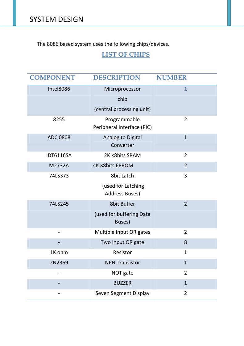
SYSTEM DESIGN
The 8086 based system uses the following chips/devices.
LIST OF CHIPS
COMPONENT DESCRIPTION NUMBER
Intel8086 Microprocessor
chip
(central processing unit)
1
8255 Programmable
Peripheral Interface (PIC) 2
ADC 0808 Analog to Digital
Converter
1
IDT6116SA 2K ×8bits SRAM 2
M2732A 4K ×8bits EPROM 2
74LS373 8bit Latch
(used for Latching
Address Buses)
3
74LS245 8bit Buffer
(used for buffering Data
Buses)
2
- Multiple Input OR gates 2
- Two Input OR gate 8
1K ohm Resistor 1
2N2369 NPN Transistor 1
- NOT gate 2
- BUZZER 1
- Seven Segment Display 2
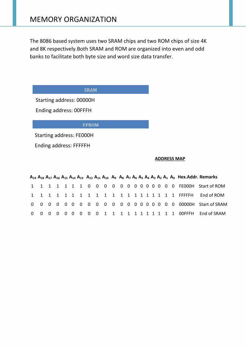
MEMORY ORGANIZATION
The 8086 based system uses two SRAM chips and two ROM chips of size 4K
and 8K respectively.Both SRAM and ROM are organized into even and odd
banks to facilitate both byte size and word size data transfer.
ADDRESS MAP
A19 A18 A17 A16 A15 A14 A13 A12 A11 A10 A9 A8 A7 A6 A5 A4 A3 A2 A1 A0 Hex.Addr. Remarks
1 1 1 1 1 1 1 0 0 0 0 0 0 0 0 0 0 0 0 0 FE000H Start of ROM
1 1 1 1 1 1 1 1 1 1 1 1 1 1 1 1 1 1 1 1 FFFFFH End of ROM
0 0 0 0 0 0 0 0 0 0 0 0 0 0 0 0 0 0 0 0 00000H Start of SRAM
0 0 0 0 0 0 0 0 0 1 1 1 1 1 1 1 1 1 1 1 00FFFH End of SRAM
SRAM
Starting address: 00000H
Ending address: 00FFFH
EPROM
Starting address: FE000H
Ending address: FFFFFH
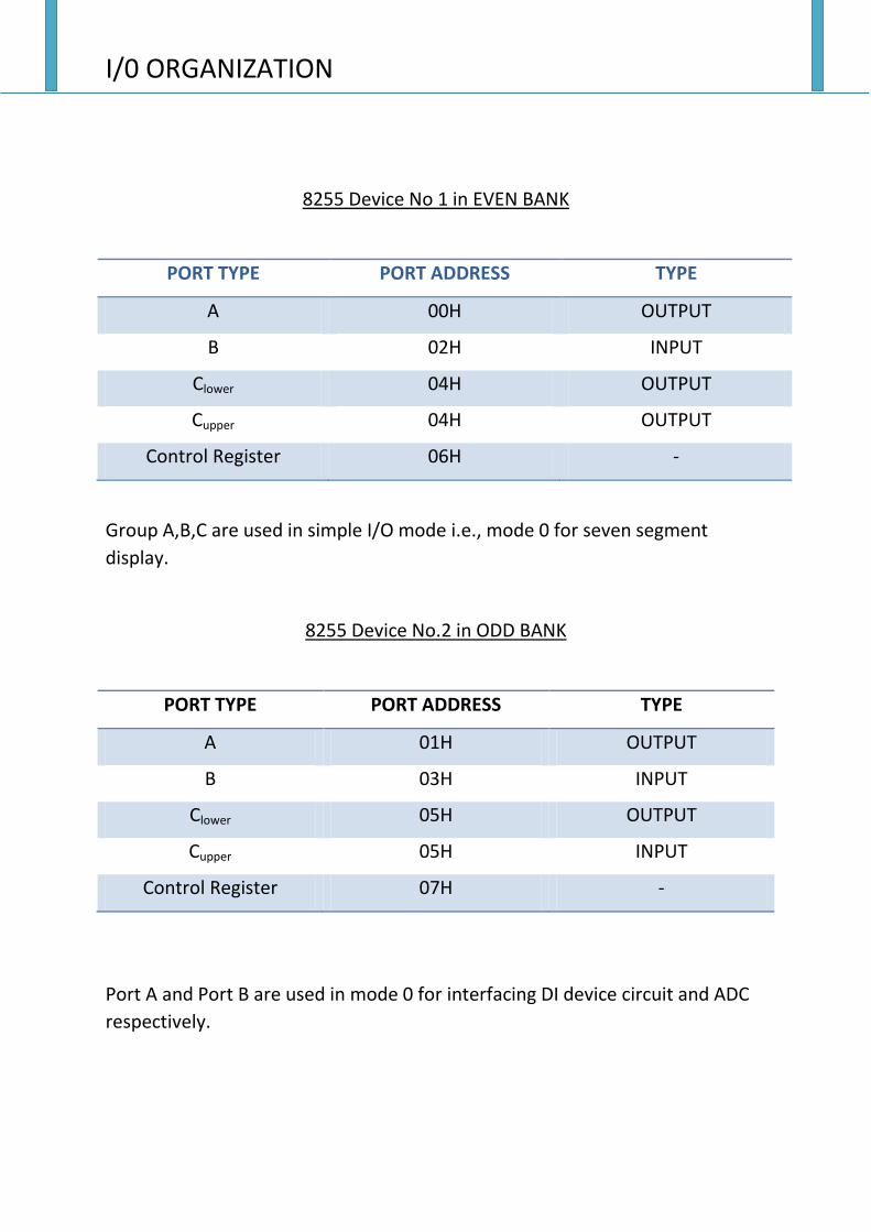
I/0 ORGANIZATION
8255 Device No 1 in EVEN BANK
PORT TYPE PORT ADDRESS TYPE
A 00H OUTPUT
B 02H INPUT
Clower 04H OUTPUT
Cupper 04H OUTPUT
Control Register 06H -
Group A,B,C are used in simple I/O mode i.e., mode 0 for seven segment
display.
8255 Device No.2 in ODD BANK
PORT TYPE PORT ADDRESS TYPE
A 01H OUTPUT
B 03H INPUT
Clower 05H OUTPUT
Cupper 05H INPUT
Control Register 07H -
Port A and Port B are used in mode 0 for interfacing DI device circuit and ADC
respectively.
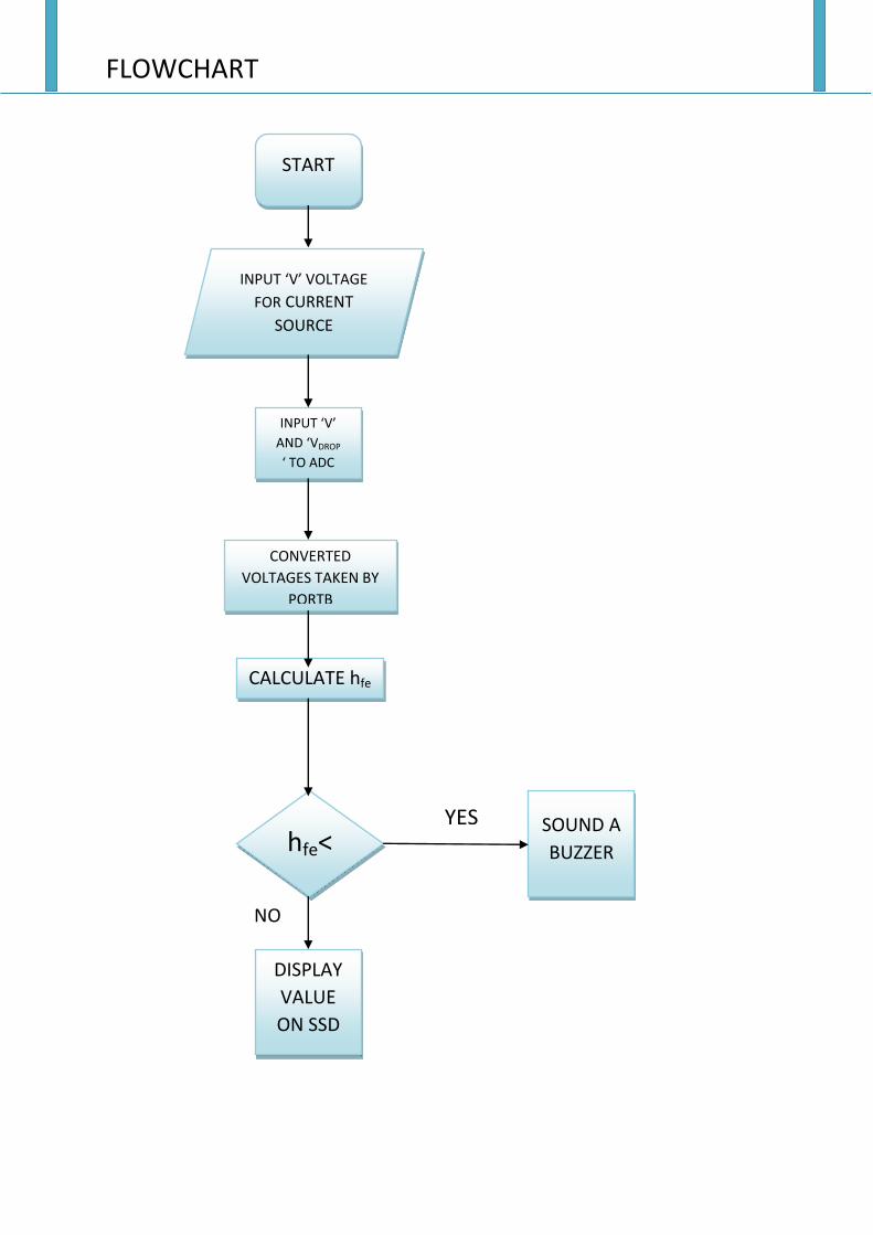
FLOWCHART
START
INPUT ‘V’ VOLTAGE
FOR CURRENT
SOURCE
INPUT ‘V’
AND ‘VDROP
‘ TO ADC
CONVERTED
VOLTAGES TAKEN BY
PORTB
CALCULATE hfe
hfe<
20 ?
SOUND A
BUZZER
DISPLAY
VALUE
ON SSD
YES
NO

ASSEMBLY LANGUAGE PROGRAM
.MODEL TINY
.DATA
.CODE
.STARTUP
MOV AL,10000010b ;initialise CReg1
OUT 06H,AL
MOV AL,10001010b ;initialise CReg2
OUT 07H,AL
CALL HFE ;Call function to calculate Hfe
CALL BUZZER ;Call funtion to ring buzzer
.exit
HFE PROC NEAR
MOV AL,01000000b
OUT 01H,AL ;AL selects measuring V FROM ADC
MOV CX,10
x2:
SUB CX,1
JNZ x2 ;TO CREATE DELAY
IN AL,02H
MOV DL,AL ;DL contains v
MOV AL,00000000b
OUT 01H,AL ;AL selects measuring Vdrop FROM ADC
MOV CX,10
x3:
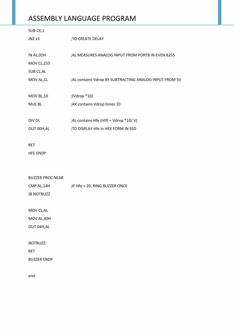
ASSEMBLY LANGUAGE PROGRAM
SUB CX,1
JNZ x3 ;TO CREATE DELAY
IN AL,02H ;AL MEASURES ANALOG INPUT FROM PORTB IN EVEN 8255
MOV CL,255
SUB CL,AL
MOV AL,CL ;AL contains Vdrop BY SUBTRACTING ANALOG INPUT FROM 5V
MOV BL,10 ;(Vdrop *10)
MUL BL ;AX contains Vdrop times 10
DIV DL ;AL contains Hfe (HFE = Vdrop *10/ V)
OUT 00H,AL ;TO DISPLAY Hfe in HEX FORM IN SSD
RET
HFE ENDP
BUZZER PROC NEAR
CMP AL,14H ;IF Hfe < 20, RING BUZZER ONCE
JB NOTBUZZ
MOV CL,AL
MOV AL,40H
OUT 04H,AL
NOTBUZZ:
RET
BUZZER ENDP
end

LIMITATIONS
• The system has not been designed for transistors with >255.
However, normal hfe range lies well below 200. • Values are displayed in hexadecimal.
• System has been designed for only one value of ‘V’ (voltage across current source). In order to get hfe for different ‘V’, we need to change value in the design.

CONCLUSIONS
• The transistor tester has been implemented as an 8086 based
system. • An alarm is sounded whenever value is less than 20.
• The seven segment displays the values of NPN transistor.
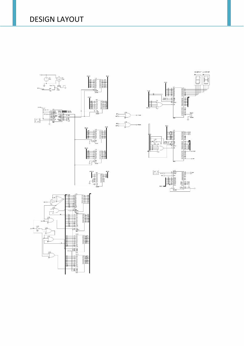
DESIGN LAYOUT


