Embed Size (px)
Citation preview
p-Type PbSe and PbS Quantum DotSolids Prepared with Short-Chain Acidsand DiacidsMohammad H. Zarghami, Yao Liu, Markelle Gibbs, Eminet Gebremichael, Christopher Webster, andMatt Law*
Department of Chemistry, Department of Chemical Engineering and Materials Science, University of California, Irvine, Irvine, California 92697
Solar cells with active layers consistingof pure films of colloidal semiconduc-tor quantum dots (QDs) are objects of
growing scientific and technologicalinterest.1�3 Thin film QD photovoltaics canbe made using large-area, low-cost solutionmethods such as roll-to-roll coating, andmay provide a pathway to ultrahigh conver-sion efficiencies via multiple exciton gen-eration (MEG).4,5 Films of electronicallycoupled QDs (often called QD solids) alsorepresent a versatile new class of granularconductors with which to investigate elec-tronic confinement, multicarrier physics,6,7
doping, and junction formation in nano-scale systems. These materials retain the op-toelectronic properties of their constitutiveQDs if gentle techniques are used to couplethe QDs together without destroying them.Thin film QD solar cells are thus distinctfrom solar cells made from sintered (bulk-like) layers of solution-deposited nanocryst-als, an approach now demonstrated withcolloidal CdTe/CdSe,8 CuInSe2 and relatedcompounds,9�11 and Cu2ZnSnS4.12�14 Costreduction, rather than efficiency enhance-ment, is the main motivation for fabricatingsintered polycrystalline active layers fromnanocrystal inks or paints.
QD photovoltaic devices based on thinfilms of PbS,15�17 PbSe,18�21 PbSexS1-x,22 andCu2S23 colloids have been demonstrated.These devices are typically prepared by dipcoating or spin coating a layer of QDs on asubstrate and then replacing the originallong-chain, insulating organic ligands witha short-chain molecule to decrease theinter-QD spacing and create a conductiveQD film.24�26 Lead salt QDs are the primaryfocus of research because they combine theprincipal features needed for facile chargetransport in QD assemblies (i.e., high densi-
ties of states, large exciton radii and dielec-tric constants, and excellent size monodis-persity) with strong light absorption andoptimal bandgap ranges for MEG27 (0.5�1.1eV). The first thin film QD solar cells utilizedan ITO/QD/metal Schottky geometry.15,18 Al-though Schottky-type cells suffer from lowvoltages, this device structure remains animportant platform for studying MEG be-cause large QDs with MEG-relevant band-gaps can be employed in the active layer.More recently, superstrate heterojunctionQD cells utilizing ZnO window layers21 orunderlayers20 have been reported. The win-dow layer design offers important effi-ciency advantages, including a shallowcharge-separating junction (which allowsfor a thicker active layer without quantumefficiency falloff at the blue end of the spec-trum) and a larger built-in voltage. State-of-the-art QD cells now achieve
*Address correspondence [email protected].
Received for review February 18, 2010and accepted March 19, 2010.
Published online April 1, 2010.10.1021/nn100339b
© 2010 American Chemical Society
ABSTRACT We show that ligand exchange with short-chain carboxylic acids (formic, acetic, and oxalic acid)
can quantitatively remove oleic acid from the surface of PbSe and PbS quantum dot (QD) films to yield p-type,
carboxylate-capped QD solids with field-effect hole mobilities in the range of 10�4�10�1 cm2 V�1 s�1. For a given
chemical treatment, PbSe devices have 10-fold higher mobilities than PbS devices because of stronger electronic
coupling among the PbSe QDs and possibly a lower density of surface traps. Long-term optical and electrical
measurements (i) show that carboxylate-capped PbSe QD films oxidize much more gradually in air than do thiol-
capped PbSe films and (ii) quantify the slower and less extensive oxidation of PbS relative to PbSe QDs. We find
that whereas the hole mobility of thiol-capped samples decreases continuously with time in air, the mobility of
carboxylate-capped films first increases by an order of magnitude over several days before slowly decreasing over
weeks. This behavior is a consequence of the more robust binding of carboxylate ligands to the QD surface, such
that adsorbed oxygen and water initially boost the hole mobility by passivating surface states and only slowly
degrade the ligand passivation to establish an oxide shell around each QD in the film. The superior hole mobilities
and oxidation resistance of formic- and acetic-treated QD solids may prove useful in constructing efficient, stable
QD photovoltaic devices.
KEYWORDS: quantum dots · PbSe · PbS · field-effect transistors · solar cells
ARTIC
LE
www.acsnano.org VOL. 4 ▪ NO. 4 ▪ 2475–2485 ▪ 2010 2475
(uncertified) power conversion efficiencies of 3�4%.20
Most of the lead salt QD cells reported to date use ei-ther 1,2-ethanedithiol (EDT) or 1,4-benzenedithiol (BDT)for ligand exchange, but these two molecules are notparticularly well suited to making efficient, stable solarcells. First, adsorbed EDT and BDT are susceptible to oxi-dation by molecular oxygen, and the resulting loss ofligand passivation triggers film oxidation and devicedegradation.25 EDT is known to quench MEG in PbSeQD films,7 while BDT-treated PbSe films have low car-rier mobilities (typically 10�4�10�3 cm2 V�1 s�1),19 per-haps in part because BDT is a relatively long ligand (S�Sdistance of �6.4 Å). Furthermore, thiol-treated Pb-chalcogenide QD films suffer from short carrier diffu-sion lengths (typically �100 nm)15,18,28 that limit the ex-ternal quantum efficiency at longer wavelengths andthus the overall device efficiency. A larger toolbox ofshort-chain ligands capable of producing robust, MEG-active QD films with long carrier diffusion lengthswould help to accelerate the development of high-performance QD photovoltaics.
Here we investigate the impact of short-chain car-boxylic acids (formic, acetic, and oxalic acid) on thestructural and electronic properties of PbSe and PbSQD solids. We show that these treatments quickly andquantitatively remove oleic acid from films of 6-nm di-ameter PbSe QDs to yield p-type, carboxylate-cappedQD solids with hole mobilities as high as 4 � 10�2 cm2
V�1 s�1 (before air exposure) when measured in a field-effect transistor (FET) geometry. Acid-treated PbSe QDfilms are much more resistant to oxidation than thiol-treated films. In particular, whereas EDT-treated FETs(initially ambipolar) become highly hole doped and un-gateable after seconds in air, acid-treated films behaveas p-FETs with hole mobilities that increase graduallyover several days in air before slowly decreasing overthe course of weeks.
Formic, acetic, and oxalic acid treatments are alsoused to prepare carboxylate-capped films of 8.8-nm di-ameter PbS QDs. Longer treatment times are requiredto remove oleate from PbS QDs, and the hole mobilitiesof the resulting FETs are 10 times lower than for theequivalent PbSe QD devices (maximum of 2 � 10�3 cm2
V�1 s�1 before air exposure). Upon air exposure, EDT-treated PbS films rapidly convert from ambipolar top-type conduction, but the subsequent decline in holemobility with storage in air is much slower than for EDT-treated PbSe FETs. In air, the hole mobilities of the acid-treated PbS FETs increase by an order of magnitude(to as high as 2 � 10�2 cm2 V�1 s�1
, 10�30 times largerthan the mobility of EDT-treated films) before peakingand slowly decreasing in a manner similar to the air-exposed PbSe FETs. Our data support a two-stage oxi-dation process in which adsorption of oxygen and wa-ter first increases the hole mobility by passivatingsurface states and subsequently decreases the mobilityby establishing an oxide shell around each QD in the
film. By combining respectable hole mobilities with im-proved surface passivation and oxidation resistance,these acid treatments may prove useful in enhancingthe performance of Schottky and heterojunction QD so-lar cells.
RESULTS AND DISCUSSIONAcid-Treated PbSe QD Films. To elucidate the impact of
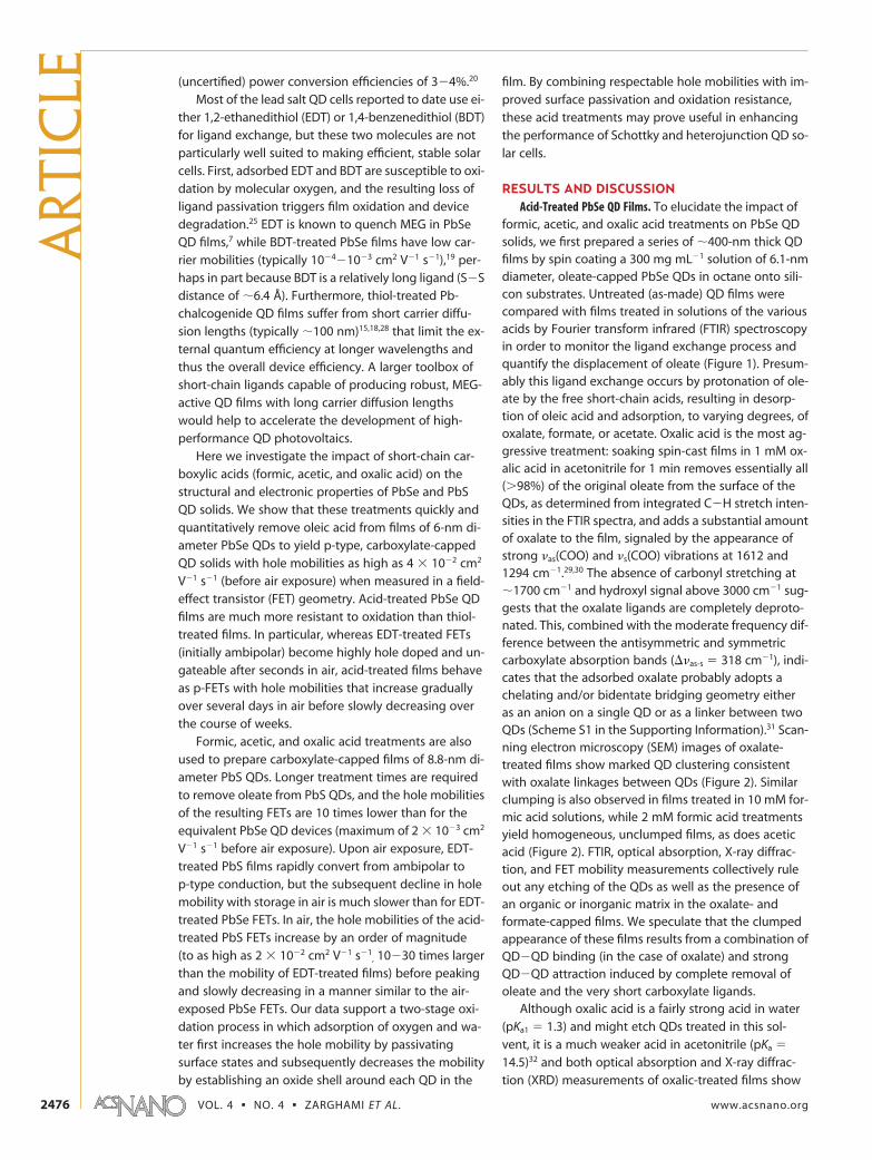
formic, acetic, and oxalic acid treatments on PbSe QDsolids, we first prepared a series of �400-nm thick QDfilms by spin coating a 300 mg mL�1 solution of 6.1-nmdiameter, oleate-capped PbSe QDs in octane onto sili-con substrates. Untreated (as-made) QD films werecompared with films treated in solutions of the variousacids by Fourier transform infrared (FTIR) spectroscopyin order to monitor the ligand exchange process andquantify the displacement of oleate (Figure 1). Presum-ably this ligand exchange occurs by protonation of ole-ate by the free short-chain acids, resulting in desorp-tion of oleic acid and adsorption, to varying degrees, ofoxalate, formate, or acetate. Oxalic acid is the most ag-gressive treatment: soaking spin-cast films in 1 mM ox-alic acid in acetonitrile for 1 min removes essentially all(�98%) of the original oleate from the surface of theQDs, as determined from integrated C�H stretch inten-sities in the FTIR spectra, and adds a substantial amountof oxalate to the film, signaled by the appearance ofstrong �as(COO) and �s(COO) vibrations at 1612 and1294 cm�1.29,30 The absence of carbonyl stretching at�1700 cm�1 and hydroxyl signal above 3000 cm�1 sug-gests that the oxalate ligands are completely deproto-nated. This, combined with the moderate frequency dif-ference between the antisymmetric and symmetriccarboxylate absorption bands (��as-s � 318 cm�1), indi-cates that the adsorbed oxalate probably adopts achelating and/or bidentate bridging geometry eitheras an anion on a single QD or as a linker between twoQDs (Scheme S1 in the Supporting Information).31 Scan-ning electron microscopy (SEM) images of oxalate-treated films show marked QD clustering consistentwith oxalate linkages between QDs (Figure 2). Similarclumping is also observed in films treated in 10 mM for-mic acid solutions, while 2 mM formic acid treatmentsyield homogeneous, unclumped films, as does aceticacid (Figure 2). FTIR, optical absorption, X-ray diffrac-tion, and FET mobility measurements collectively ruleout any etching of the QDs as well as the presence ofan organic or inorganic matrix in the oxalate- andformate-capped films. We speculate that the clumpedappearance of these films results from a combination ofQD�QD binding (in the case of oxalate) and strongQD�QD attraction induced by complete removal ofoleate and the very short carboxylate ligands.
Although oxalic acid is a fairly strong acid in water(pKa1 � 1.3) and might etch QDs treated in this sol-vent, it is a much weaker acid in acetonitrile (pKa �
14.5)32 and both optical absorption and X-ray diffrac-tion (XRD) measurements of oxalic-treated films show
ART
ICLE
VOL. 4 ▪ NO. 4 ▪ ZARGHAMI ET AL. www.acsnano.org2476
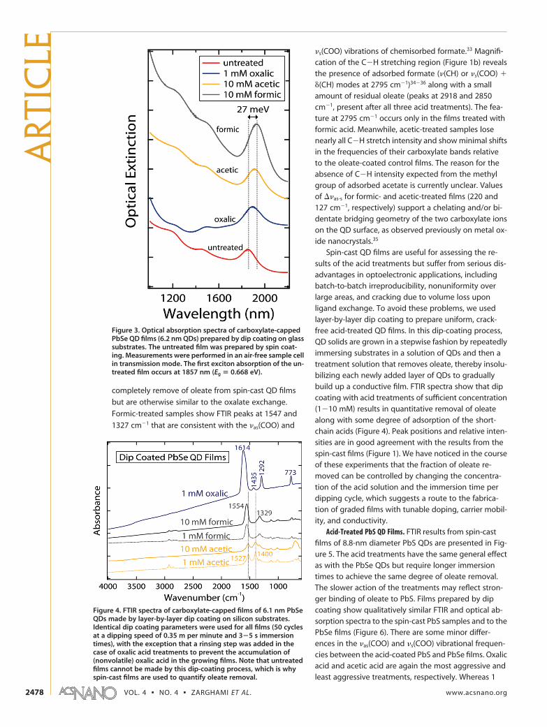
that no QD etching occurs. Absorption spectra of
oxalate-coated films on glass substrates show a 14
meV redshift of the first excitonic peak upon exchange
of oleate with oxalate (Figure 3); etching would result in
a blueshift of �75 meV for even a 5 Å decrease in QD di-
ameter. This redshift, which is similar in magnitude to
redshifts observed after treating PbSe QD solids in for-
mic or acetic acid (Figure 3), hydrazine,26 or dithiols,25
arises from a combination of increased average dielec-
tric constant and enhanced inter-QD electronic cou-
pling when oleate is removed and the QDs pack closer
together within a film.25 Any redshift of the excitonic
energy due to decreased electronic confinement from
the ligand exchange itselfOoften observed when ole-
ate is replaced with amines or thiolsOis probably insig-
nificant here because oleate is replaced by other car-
boxylates, leaving the molecular environment at the QD
surface largely unaltered. XRD measurements confirm
that the QD size is unchanged (to within �1 Å) by ex-
posure to 1 mM oxalic acid, even for soaking times as
long as 20 min (the longest studied) (Supporting Infor-
mation, Figure S4). On the basis of such optical and XRD
data, we conclude that each of the three acid treat-
ments replaces oleate without etching the QDs, unsur-
prising given the small dissociation constants of these
carboxylic acids in acetonitrile.
Formic acid and acetic acid treatments require
higher concentrations and longer immersion times to
Figure 1. FTIR spectra of films of 6.1 nm PbSe QDs made by spin-casting onto silicon substrates and treated in 1 mM oxalic,10 mM acetic, or 10 mM formic acid solutions in acetonitrile: (a) survey scans for three films and an untreated oleate-cappedcontrol film; (b) magnification of the C�H stretching region of the treated films. All films were 400 nm-thick before treat-ment. The sloping backgrounds are caused by optical interference effects (see Figures S1�S3 in the Supporting Informa-tion for additional spectra).
Figure 2. SEM images of �100-nm thick films of 6.1 nm carboxylate-capped PbSe QDs prepared by dip coating on siliconsubstrates (see Supporting Information Figure S5 for an image of an untreated film prepared by spin coating).
ARTIC
LE
www.acsnano.org VOL. 4 ▪ NO. 4 ▪ 2475–2485 ▪ 2010 2477
completely remove of oleate from spin-cast QD films
but are otherwise similar to the oxalate exchange.
Formic-treated samples show FTIR peaks at 1547 and
1327 cm�1 that are consistent with the �as(COO) and
�s(COO) vibrations of chemisorbed formate.33 Magnifi-cation of the C�H stretching region (Figure 1b) revealsthe presence of adsorbed formate (�(CH) or �s(COO)
(CH) modes at 2795 cm�1)34�36 along with a smallamount of residual oleate (peaks at 2918 and 2850cm�1, present after all three acid treatments). The fea-ture at 2795 cm�1 occurs only in the films treated withformic acid. Meanwhile, acetic-treated samples losenearly all C�H stretch intensity and show minimal shiftsin the frequencies of their carboxylate bands relativeto the oleate-coated control films. The reason for theabsence of C�H intensity expected from the methylgroup of adsorbed acetate is currently unclear. Valuesof ��as-s for formic- and acetic-treated films (220 and127 cm�1, respectively) support a chelating and/or bi-dentate bridging geometry of the two carboxylate ionson the QD surface, as observed previously on metal ox-ide nanocrystals.35
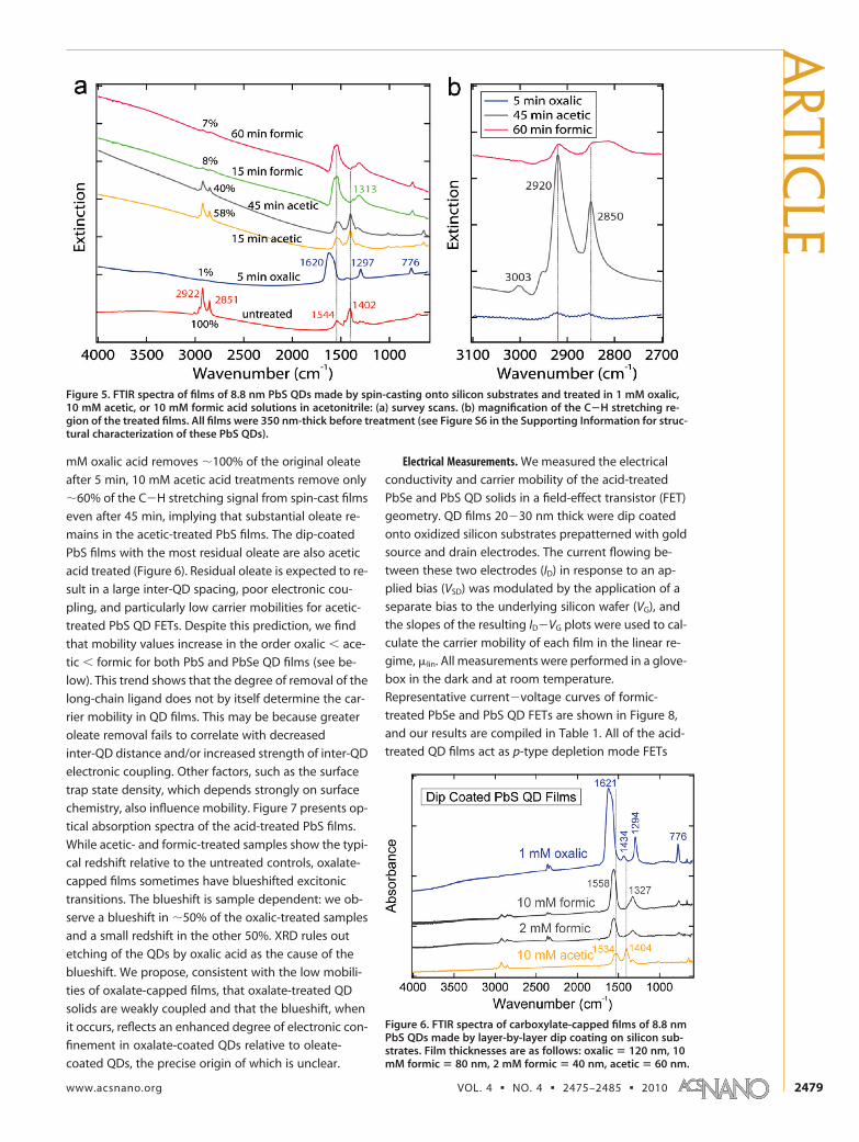
Spin-cast QD films are useful for assessing the re-sults of the acid treatments but suffer from serious dis-advantages in optoelectronic applications, includingbatch-to-batch irreproducibility, nonuniformity overlarge areas, and cracking due to volume loss uponligand exchange. To avoid these problems, we usedlayer-by-layer dip coating to prepare uniform, crack-free acid-treated QD films. In this dip-coating process,QD solids are grown in a stepwise fashion by repeatedlyimmersing substrates in a solution of QDs and then atreatment solution that removes oleate, thereby insolu-bilizing each newly added layer of QDs to graduallybuild up a conductive film. FTIR spectra show that dipcoating with acid treatments of sufficient concentration(1�10 mM) results in quantitative removal of oleatealong with some degree of adsorption of the short-chain acids (Figure 4). Peak positions and relative inten-sities are in good agreement with the results from thespin-cast films (Figure 1). We have noticed in the courseof these experiments that the fraction of oleate re-moved can be controlled by changing the concentra-tion of the acid solution and the immersion time perdipping cycle, which suggests a route to the fabrica-tion of graded films with tunable doping, carrier mobil-ity, and conductivity.
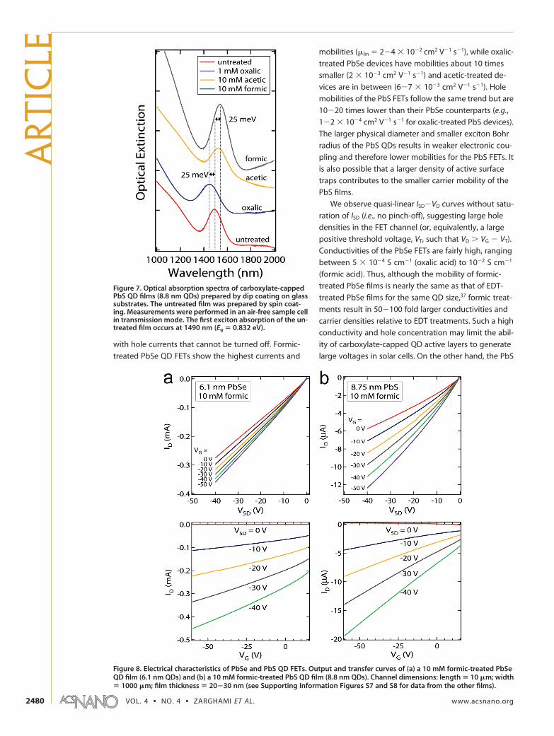
Acid-Treated PbS QD Films. FTIR results from spin-castfilms of 8.8-nm diameter PbS QDs are presented in Fig-ure 5. The acid treatments have the same general effectas with the PbSe QDs but require longer immersiontimes to achieve the same degree of oleate removal.The slower action of the treatments may reflect stron-ger binding of oleate to PbS. Films prepared by dipcoating show qualitatively similar FTIR and optical ab-sorption spectra to the spin-cast PbS samples and to thePbSe films (Figure 6). There are some minor differ-ences in the �as(COO) and �s(COO) vibrational frequen-cies between the acid-coated PbS and PbSe films. Oxalicacid and acetic acid are again the most aggressive andleast aggressive treatments, respectively. Whereas 1
Figure 3. Optical absorption spectra of carboxylate-cappedPbSe QD films (6.2 nm QDs) prepared by dip coating on glasssubstrates. The untreated film was prepared by spin coat-ing. Measurements were performed in an air-free sample cellin transmission mode. The first exciton absorption of the un-treated film occurs at 1857 nm (Eg � 0.668 eV).
Figure 4. FTIR spectra of carboxylate-capped films of 6.1 nm PbSeQDs made by layer-by-layer dip coating on silicon substrates.Identical dip coating parameters were used for all films (50 cyclesat a dipping speed of 0.35 m per minute and 3�5 s immersiontimes), with the exception that a rinsing step was added in thecase of oxalic acid treatments to prevent the accumulation of(nonvolatile) oxalic acid in the growing films. Note that untreatedfilms cannot be made by this dip-coating process, which is whyspin-cast films are used to quantify oleate removal.
ART
ICLE
VOL. 4 ▪ NO. 4 ▪ ZARGHAMI ET AL. www.acsnano.org2478
mM oxalic acid removes �100% of the original oleate
after 5 min, 10 mM acetic acid treatments remove only
�60% of the C�H stretching signal from spin-cast films
even after 45 min, implying that substantial oleate re-
mains in the acetic-treated PbS films. The dip-coated
PbS films with the most residual oleate are also acetic
acid treated (Figure 6). Residual oleate is expected to re-
sult in a large inter-QD spacing, poor electronic cou-
pling, and particularly low carrier mobilities for acetic-
treated PbS QD FETs. Despite this prediction, we find
that mobility values increase in the order oxalic � ace-
tic � formic for both PbS and PbSe QD films (see be-
low). This trend shows that the degree of removal of the
long-chain ligand does not by itself determine the car-
rier mobility in QD films. This may be because greater
oleate removal fails to correlate with decreased
inter-QD distance and/or increased strength of inter-QD
electronic coupling. Other factors, such as the surface
trap state density, which depends strongly on surface
chemistry, also influence mobility. Figure 7 presents op-
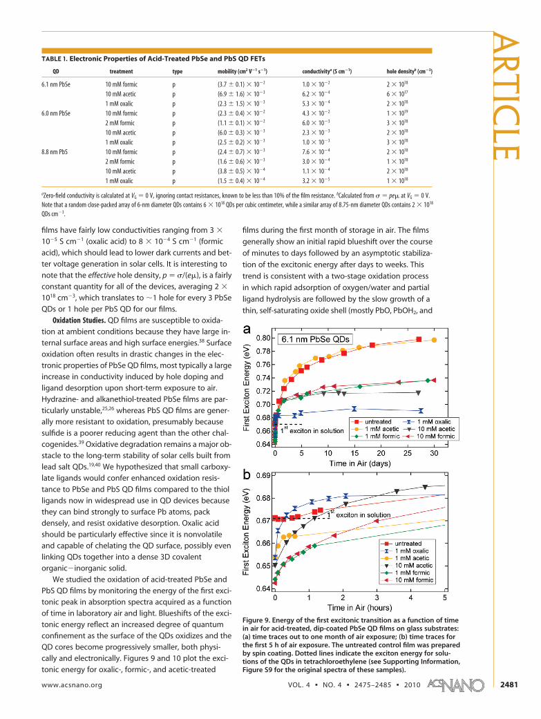
tical absorption spectra of the acid-treated PbS films.
While acetic- and formic-treated samples show the typi-
cal redshift relative to the untreated controls, oxalate-
capped films sometimes have blueshifted excitonic
transitions. The blueshift is sample dependent: we ob-
serve a blueshift in �50% of the oxalic-treated samples
and a small redshift in the other 50%. XRD rules out
etching of the QDs by oxalic acid as the cause of the
blueshift. We propose, consistent with the low mobili-
ties of oxalate-capped films, that oxalate-treated QD
solids are weakly coupled and that the blueshift, when
it occurs, reflects an enhanced degree of electronic con-
finement in oxalate-coated QDs relative to oleate-
coated QDs, the precise origin of which is unclear.
Electrical Measurements. We measured the electrical
conductivity and carrier mobility of the acid-treated
PbSe and PbS QD solids in a field-effect transistor (FET)
geometry. QD films 20�30 nm thick were dip coated
onto oxidized silicon substrates prepatterned with gold
source and drain electrodes. The current flowing be-
tween these two electrodes (ID) in response to an ap-
plied bias (VSD) was modulated by the application of a
separate bias to the underlying silicon wafer (VG), and
the slopes of the resulting ID�VG plots were used to cal-
culate the carrier mobility of each film in the linear re-
gime, �lin. All measurements were performed in a glove-
box in the dark and at room temperature.
Representative current�voltage curves of formic-
treated PbSe and PbS QD FETs are shown in Figure 8,
and our results are compiled in Table 1. All of the acid-
treated QD films act as p-type depletion mode FETs
Figure 6. FTIR spectra of carboxylate-capped films of 8.8 nmPbS QDs made by layer-by-layer dip coating on silicon sub-strates. Film thicknesses are as follows: oxalic � 120 nm, 10mM formic � 80 nm, 2 mM formic � 40 nm, acetic � 60 nm.
Figure 5. FTIR spectra of films of 8.8 nm PbS QDs made by spin-casting onto silicon substrates and treated in 1 mM oxalic,10 mM acetic, or 10 mM formic acid solutions in acetonitrile: (a) survey scans. (b) magnification of the C�H stretching re-gion of the treated films. All films were 350 nm-thick before treatment (see Figure S6 in the Supporting Information for struc-tural characterization of these PbS QDs).
ARTIC
LE
www.acsnano.org VOL. 4 ▪ NO. 4 ▪ 2475–2485 ▪ 2010 2479
with hole currents that cannot be turned off. Formic-
treated PbSe QD FETs show the highest currents and
mobilities (�lin � 2�4 � 10�2 cm2 V�1 s�1), while oxalic-
treated PbSe devices have mobilities about 10 times
smaller (2 � 10�3 cm2 V�1 s�1) and acetic-treated de-
vices are in between (6�7 � 10�3 cm2 V�1 s�1). Hole
mobilities of the PbS FETs follow the same trend but are
10�20 times lower than their PbSe counterparts (e.g.,
1�2 � 10�4 cm2 V�1 s�1 for oxalic-treated PbS devices).
The larger physical diameter and smaller exciton Bohr
radius of the PbS QDs results in weaker electronic cou-
pling and therefore lower mobilities for the PbS FETs. It
is also possible that a larger density of active surface
traps contributes to the smaller carrier mobility of the
PbS films.
We observe quasi-linear ISD�VD curves without satu-
ration of ISD (i.e., no pinch-off), suggesting large hole
densities in the FET channel (or, equivalently, a large
positive threshold voltage, VT, such that VD � VG � VT).
Conductivities of the PbSe FETs are fairly high, ranging
between 5 � 10�4 S cm�1 (oxalic acid) to 10�2 S cm�1
(formic acid). Thus, although the mobility of formic-
treated PbSe films is nearly the same as that of EDT-
treated PbSe films for the same QD size,37 formic treat-
ments result in 50�100 fold larger conductivities and
carrier densities relative to EDT treatments. Such a high
conductivity and hole concentration may limit the abil-
ity of carboxylate-capped QD active layers to generate
large voltages in solar cells. On the other hand, the PbS
Figure 7. Optical absorption spectra of carboxylate-cappedPbS QD films (8.8 nm QDs) prepared by dip coating on glasssubstrates. The untreated film was prepared by spin coat-ing. Measurements were performed in an air-free sample cellin transmission mode. The first exciton absorption of the un-treated film occurs at 1490 nm (Eg � 0.832 eV).
Figure 8. Electrical characteristics of PbSe and PbS QD FETs. Output and transfer curves of (a) a 10 mM formic-treated PbSeQD film (6.1 nm QDs) and (b) a 10 mM formic-treated PbS QD film (8.8 nm QDs). Channel dimensions: length � 10 �m; width� 1000 �m; film thickness � 20�30 nm (see Supporting Information Figures S7 and S8 for data from the other films).
ART
ICLE
VOL. 4 ▪ NO. 4 ▪ ZARGHAMI ET AL. www.acsnano.org2480
films have fairly low conductivities ranging from 3 �
10�5 S cm�1 (oxalic acid) to 8 � 10�4 S cm�1 (formic
acid), which should lead to lower dark currents and bet-
ter voltage generation in solar cells. It is interesting to
note that the effective hole density, p � /(e�), is a fairly
constant quantity for all of the devices, averaging 2 �
1018 cm�3, which translates to �1 hole for every 3 PbSe
QDs or 1 hole per PbS QD for our films.
Oxidation Studies. QD films are susceptible to oxida-
tion at ambient conditions because they have large in-
ternal surface areas and high surface energies.38 Surface
oxidation often results in drastic changes in the elec-
tronic properties of PbSe QD films, most typically a large
increase in conductivity induced by hole doping and
ligand desorption upon short-term exposure to air.
Hydrazine- and alkanethiol-treated PbSe films are par-
ticularly unstable,25,26 whereas PbS QD films are gener-
ally more resistant to oxidation, presumably because
sulfide is a poorer reducing agent than the other chal-
cogenides.39 Oxidative degradation remains a major ob-
stacle to the long-term stability of solar cells built from
lead salt QDs.19,40 We hypothesized that small carboxy-
late ligands would confer enhanced oxidation resis-
tance to PbSe and PbS QD films compared to the thiol
ligands now in widespread use in QD devices because
they can bind strongly to surface Pb atoms, pack
densely, and resist oxidative desorption. Oxalic acid
should be particularly effective since it is nonvolatile
and capable of chelating the QD surface, possibly even
linking QDs together into a dense 3D covalent
organic�inorganic solid.
We studied the oxidation of acid-treated PbSe and
PbS QD films by monitoring the energy of the first exci-
tonic peak in absorption spectra acquired as a function
of time in laboratory air and light. Blueshifts of the exci-
tonic energy reflect an increased degree of quantum
confinement as the surface of the QDs oxidizes and the
QD cores become progressively smaller, both physi-
cally and electronically. Figures 9 and 10 plot the exci-
tonic energy for oxalic-, formic-, and acetic-treated
films during the first month of storage in air. The films
generally show an initial rapid blueshift over the course
of minutes to days followed by an asymptotic stabiliza-
tion of the excitonic energy after days to weeks. This
trend is consistent with a two-stage oxidation process
in which rapid adsorption of oxygen/water and partial
ligand hydrolysis are followed by the slow growth of a
thin, self-saturating oxide shell (mostly PbO, PbOH2, and
Figure 9. Energy of the first excitonic transition as a function of timein air for acid-treated, dip-coated PbSe QD films on glass substrates:(a) time traces out to one month of air exposure; (b) time traces forthe first 5 h of air exposure. The untreated control film was preparedby spin coating. Dotted lines indicate the exciton energy for solu-tions of the QDs in tetrachloroethylene (see Supporting Information,Figure S9 for the original spectra of these samples).
TABLE 1. Electronic Properties of Acid-Treated PbSe and PbS QD FETs
QD treatment type mobility (cm2 V�1 s�1) conductivitya (S cm�1) hole densityb (cm�3)
6.1 nm PbSe 10 mM formic p (3.7 � 0.1) � 10�2 1.0 � 10�2 2 � 1018
10 mM acetic p (6.9 � 1.6) � 10�3 6.2 � 10�4 6 � 1017
1 mM oxalic p (2.3 � 1.5) � 10�3 5.3 � 10�4 2 � 1018
6.0 nm PbSe 10 mM formic p (2.3 � 0.4) � 10�2 4.3 � 10�2 1 � 1019
2 mM formic p (1.1 � 0.1) � 10�2 6.0 � 10�3 3 � 1018
10 mM acetic p (6.0 � 0.3) � 10�3 2.3 � 10�3 2 � 1018
1 mM oxalic p (2.5 � 0.2) � 10�3 1.0 � 10�3 3 � 1018
8.8 nm PbS 10 mM formic p (2.4 � 0.7) � 10�3 7.6 � 10�4 2 � 1018
2 mM formic p (1.6 � 0.6) � 10�3 3.0 � 10�4 1 � 1018
10 mM acetic p (3.8 � 0.5) � 10�4 1.1 � 10�4 2 � 1018
1 mM oxalic p (1.5 � 0.4) � 10�4 3.2 � 10�5 1 � 1018
aZero-field conductivity is calculated at VG � 0 V, ignoring contact resistances, known to be less than 10% of the film resistance. bCalculated from � pe� at VG � 0 V.Note that a random close-packed array of 6-nm diameter QDs contains 6 � 1018 QDs per cubic centimeter, while a similar array of 8.75-nm diameter QDs contains 2 � 1018
QDs cm�3.
ARTIC
LE
www.acsnano.org VOL. 4 ▪ NO. 4 ▪ 2475–2485 ▪ 2010 2481
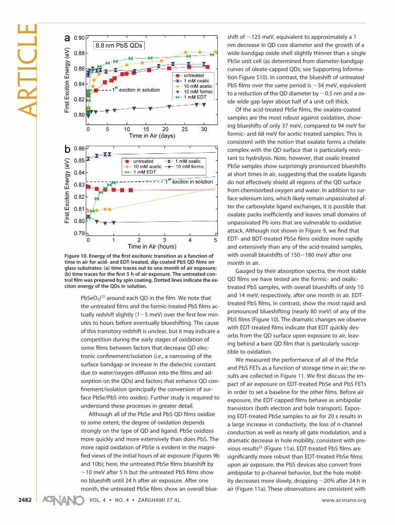
PbSeO3)25 around each QD in the film. We note that
the untreated films and the formic-treated PbS films ac-
tually redshift slightly (1�5 meV) over the first few min-
utes to hours before eventually blueshifting. The cause
of this transitory redshift is unclear, but it may indicate a
competition during the early stages of oxidation of
some films between factors that decrease QD elec-
tronic confinement/isolation (i.e., a narrowing of the
surface bandgap or increase in the dielectric constant
due to water/oxygen diffusion into the films and ad-
sorption on the QDs) and factors that enhance QD con-
finement/isolation (principally the conversion of sur-
face PbSe/PbS into oxides). Further study is required to
understand these processes in greater detail.
Although all of the PbSe and PbS QD films oxidize
to some extent, the degree of oxidation depends
strongly on the type of QD and ligand. PbSe oxidizes
more quickly and more extensively than does PbS. The
more rapid oxidation of PbSe is evident in the magni-
fied views of the initial hours of air exposure (Figures 9b
and 10b); here, the untreated PbSe films blueshift by
�10 meV after 5 h but the untreated PbS films show
no blueshift until 24 h after air exposure. After one
month, the untreated PbSe films show an overall blue-
shift of �125 meV, equivalent to approximately a 1nm decrease in QD core diameter and the growth of awide-bandgap oxide shell slightly thinner than a singlePbSe unit cell (as determined from diameter-bandgapcurves of oleate-capped QDs; see Supporting Informa-tion Figure S10). In contrast, the blueshift of untreatedPbS films over the same period is �34 meV, equivalentto a reduction of the QD diameter by �0.5 nm and a ox-ide wide gap layer about half of a unit cell thick.
Of the acid-treated PbSe films, the oxalate-coatedsamples are the most robust against oxidation, show-ing blueshifts of only 37 meV, compared to 94 meV forformic- and 68 meV for acetic-treated samples. This isconsistent with the notion that oxalate forms a chelatecomplex with the QD surface that is particularly resis-tant to hydrolysis. Note, however, that oxalic-treatedPbSe samples show surprisingly pronounced blueshiftsat short times in air, suggesting that the oxalate ligandsdo not effectively shield all regions of the QD surfacefrom chemisorbed oxygen and water. In addition to sur-face selenium ions, which likely remain unpassivated af-ter the carboxylate ligand exchanges, it is possible thatoxalate packs inefficiently and leaves small domains ofunpassivated Pb ions that are vulnerable to oxidativeattack. Although not shown in Figure 9, we find thatEDT- and BDT-treated PbSe films oxidize more rapidlyand extensively than any of the acid-treated samples,with overall blueshifts of 150�180 meV after onemonth in air.
Gauged by their absorption spectra, the most stableQD films we have tested are the formic- and oxalic-treated PbS samples, with overall blueshifts of only 10and 14 meV, respectively, after one month in air. EDT-treated PbS films, in contrast, show the most rapid andpronounced blueshifting (nearly 80 meV) of any of thePbS films (Figure 10). The dramatic changes we observewith EDT-treated films indicate that EDT quickly des-orbs from the QD surface upon exposure to air, leav-ing behind a bare QD film that is particularly suscep-tible to oxidation.
We measured the performance of all of the PbSeand PbS FETs as a function of storage time in air; the re-sults are collected in Figure 11. We first discuss the im-pact of air exposure on EDT-treated PbSe and PbS FETsin order to set a baseline for the other films. Before airexposure, the EDT-capped films behave as ambipolartransistors (both electron and hole transport). Expos-ing EDT-treated PbSe samples to air for 20 s results ina large increase in conductivity, the loss of n-channelconduction as well as nearly all gate modulation, and adramatic decrease in hole mobility, consistent with pre-vious results25 (Figure 11a). EDT-treated PbS films aresignificantly more robust than EDT-treated PbSe films:upon air exposure, the PbS devices also convert fromambipolar to p-channel behavior, but the hole mobil-ity decreases more slowly, dropping �20% after 24 h inair (Figure 11a). These observations are consistent with
Figure 10. Energy of the first excitonic transition as a function oftime in air for acid- and EDT-treated, dip-coated PbS QD films onglass substrates: (a) time traces out to one month of air exposure;(b) time traces for the first 5 h of air exposure. The untreated con-trol film was prepared by spin coating. Dotted lines indicate the ex-citon energy of the QDs in solution.
ART
ICLE
VOL. 4 ▪ NO. 4 ▪ ZARGHAMI ET AL. www.acsnano.org2482
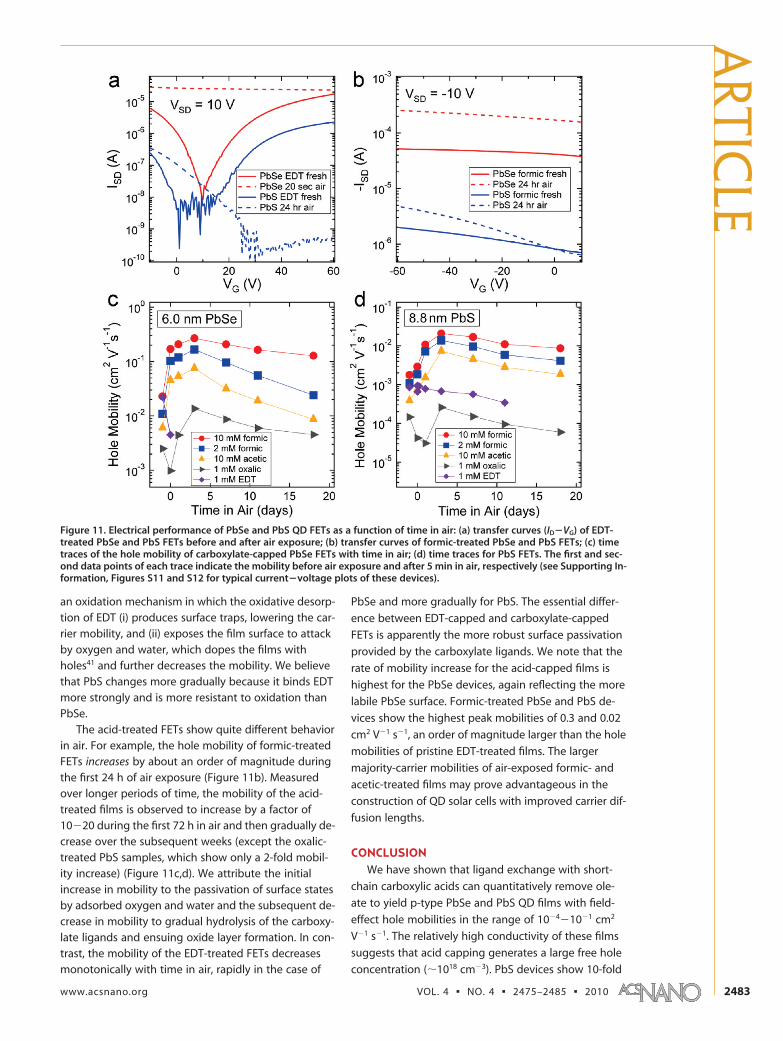
an oxidation mechanism in which the oxidative desorp-tion of EDT (i) produces surface traps, lowering the car-rier mobility, and (ii) exposes the film surface to attackby oxygen and water, which dopes the films withholes41 and further decreases the mobility. We believethat PbS changes more gradually because it binds EDTmore strongly and is more resistant to oxidation thanPbSe.
The acid-treated FETs show quite different behaviorin air. For example, the hole mobility of formic-treatedFETs increases by about an order of magnitude duringthe first 24 h of air exposure (Figure 11b). Measuredover longer periods of time, the mobility of the acid-treated films is observed to increase by a factor of10�20 during the first 72 h in air and then gradually de-crease over the subsequent weeks (except the oxalic-treated PbS samples, which show only a 2-fold mobil-ity increase) (Figure 11c,d). We attribute the initialincrease in mobility to the passivation of surface statesby adsorbed oxygen and water and the subsequent de-crease in mobility to gradual hydrolysis of the carboxy-late ligands and ensuing oxide layer formation. In con-trast, the mobility of the EDT-treated FETs decreasesmonotonically with time in air, rapidly in the case of
PbSe and more gradually for PbS. The essential differ-
ence between EDT-capped and carboxylate-capped
FETs is apparently the more robust surface passivation
provided by the carboxylate ligands. We note that the
rate of mobility increase for the acid-capped films is
highest for the PbSe devices, again reflecting the more
labile PbSe surface. Formic-treated PbSe and PbS de-
vices show the highest peak mobilities of 0.3 and 0.02
cm2 V�1 s�1, an order of magnitude larger than the hole
mobilities of pristine EDT-treated films. The larger
majority-carrier mobilities of air-exposed formic- and
acetic-treated films may prove advantageous in the
construction of QD solar cells with improved carrier dif-
fusion lengths.
CONCLUSIONWe have shown that ligand exchange with short-
chain carboxylic acids can quantitatively remove ole-
ate to yield p-type PbSe and PbS QD films with field-
effect hole mobilities in the range of 10�4�10�1 cm2
V�1 s�1. The relatively high conductivity of these films
suggests that acid capping generates a large free hole
concentration (�1018 cm�3). PbS devices show 10-fold
Figure 11. Electrical performance of PbSe and PbS QD FETs as a function of time in air: (a) transfer curves (ID�VG) of EDT-treated PbSe and PbS FETs before and after air exposure; (b) transfer curves of formic-treated PbSe and PbS FETs; (c) timetraces of the hole mobility of carboxylate-capped PbSe FETs with time in air; (d) time traces for PbS FETs. The first and sec-ond data points of each trace indicate the mobility before air exposure and after 5 min in air, respectively (see Supporting In-formation, Figures S11 and S12 for typical current�voltage plots of these devices).
ARTIC
LE
www.acsnano.org VOL. 4 ▪ NO. 4 ▪ 2475–2485 ▪ 2010 2483
lower mobilities than PbSe devices made using thesame film treatment. PbS field-effect transistors pre-pared with EDT are much more stable in air than EDT-treated PbSe QD films, but the n-channels of both filmsdisappear upon air exposure and the hole mobilities de-crease monotonically with time in air (at very differentrates). Long-term FET measurements demonstrate thatthe hole mobilities of acid-treated films exposed to airincrease by a factor of 10�20 before gradually decreas-ing. At the same time, optical absorption spectra ofthe acid-treated films show a monotonic, treatment-dependent increase in exciton energy and carrier con-
finement as oxidation unfolds. Our results thereforeshow that the mobility of QD films can increase de-spite a concurrent decrease in inter-QD coupling. Thiscan be understood in the case of acid-treated PbSe andPbS FETs if initial oxidation results in the passivation ofsurface traps and if oxidation of the film surface is rela-tively slow because the carboxylate ligands are stronglybound. More detailed future studies of the interplayamong surface chemistry, oxidation, and the mobilityand lifetime of charge carriers in QD films will providevaluable guidance for the fabrication of efficient andtruly stable QD photovoltaic devices.
METHODSMaterials. Lead oxide (PbO, 99.999%), selenium (99.99%), oleic
acid (OA, tech. grade, 90%), diphenylphosphine (DPP, 98%),1-octadecene (ODE, 90%), acetic acid (glacial, 99.99%), oxalicacid (anhydrous), and anhydrous solvents were purchased fromAldrich and used as received. Bis(trimethylsilyl) sulfide (TMS) wasacquired from Gelest, while trioctylphosphine (TOP, technicalgrade, � 90%) and 1,2-ethanedithiol (EDT, � 98%) were fromFluka and formic acid (99%) was from Acros.
QD Synthesis. PbSe QDs were synthesized and purified usingstandard air-free techniques. In a typical synthesis, 1.09 g PbO(4.9 mmol), 3.45 g OA (12.2 mmol), and 13.25 g ODE were de-gassed in a three-neck flask for 10 min at room temperature and10 min at 100 °C, then heated at 180 °C for at least 1 h underflowing nitrogen to dissolve the PbO and dry the solution. Next,15 mL of a 1 M TOP-Se solution (15 mmol) containing 0.13 mLDPP was rapidly injected into the hot lead oleate solution. PbSeQD nucleation was instantaneous. Once the desired growth timehad elapsed (1�20 min), the reaction was quenched with a wa-ter bath and the injection of 15 mL of dry hexane. The QDs werepurified by precipitation three times in hexane/ethanol andstored in a glovebox.
PbS QDs were prepared using a procedure adapted fromHines.42 Briefly, 0.65 g PbO (2.9 mmol) and 12.7 g OA (57 mmol)were mixed, degassed as described above, heated at 150 °C for atleast 1 h, and cooled to 100 °C before a solution of 0.3 mL TMS(1.4 mmol) in 5.6 g ODE was rapidly injected. The reaction wasimmediately quenched with a water bath and the QDs were pu-rified similarly to the PbSe QD samples.
Fabrication of QD Films. Both spin coating and dip coating wereused to make QD films. Films were spin coated inside of a glove-box from 300 mg mL�1 solutions of PbSe or PbS QDs in octane,then immersed in 5 mL of a 1, 2, or 10 mM solution of the appro-priate short-chain acid in dry acetonitrile for a given time.Samples treated in oxalic acid were rinsed with dry acetonitrileto remove any oxalic acid residue (oxalic acid is nonvolatile atroom temperature).
Films were dip coated using a layer-by-layer procedure de-scribed in detail elsewhere25,28 with a mechanical dip coatermounted inside of a glovebox (DC Multi-4, Nima Technology).The substrates (prepatterned FET substrates, glass slides, ordouble-side-polished i-Si(100) wafers, cleaned by sonication inacetone followed by rinses in acetone and hexane and dryingunder an N2 flow) were repetitively dipped into a 2 mg mL�1 so-lution of QDs in dry hexane and then a 1, 2, or 10 mM solutionof the appropriate short-chain acid in dry acetonitrile. In the caseof the oxalic acid treatments, a third beaker containing pure ac-etonitrile was used to rinse the films after each dip in the oxalicacid solution. We fabricated films with thicknesses in the range of20�450 nm (thin for FETs and thick for UV�vis and FTIR stud-ies).
Characterization. Transmission electron microscopy (TEM) char-acterization was performed on a Philips CM 20 operating at 200kV. A Zeiss Ultra 55 Plus field emission scanning electron micro-scope (SEM) was used to image the QD films. Optical absorption
data were acquired with a PerkinElmer Lambda 950 spectropho-tometer equipped with an integrating sphere. Fourier trans-form infrared (FTIR) data were taken with a Jasco 4100 FTIR spec-trometer. A Rigaku Ultima III diffractometer was used for X-raydiffraction measurements.
Field-Effect Transistor Measurements. QD films were dip cast ontodegenerately doped silicon substrates that were coated with a200-nm-thick thermal SiO2 gate oxide and patterned withsource/drain electrodes (5 nm Ti/35 nm Au; 5, 10, or 25 �m chan-nel length, 1000 �m width). Film thicknesses of 20�35 nm (3�6QD diameters) were used. Unwanted areas of each film were re-moved with a swab. FET measurements were performed in aglovebox with a homemade probe station using a Keithley2636A dual-channel SourceMeter driven by LabVIEW software.Consistent with previous results26,36 we found the source-draincurrents of these FETs to be time dependent (quasi-exponentialdecay) upon a change in gate voltage. ID�VSD and ID�VG curveswere therefore acquired as quickly as possible (0.4�0.8 s) tominimize the distorting effects of the slow transient process(es)on the output and transfer characteristics of the devices. Electronand hole mobilities �lin were calculated from transfer curves ac-quired at positive and negative VSD, respectively, according tothe gradual channel approximation equation in the linearregime,
where W is the channel width, L the channel length, and Cox isthe capacitance per unit area of the gate oxide. The carrier mo-bilities reported here are averages of 3�6 devices.
Acknowledgment. We thank Joseph Luther for helpful discus-sions, Robert Corn for use of the FTIR spectrometer, and the UCIPhysical Sciences Center for Solar Energy for supporting thiswork. The authors acknowledge the provision of the instrumen-tation in the Carl Zeiss Center of Excellence at UCI by Carl ZeissSMT. M.L. is supported by the Center for Advanced Solar Photo-physics, an Energy Frontier Research Center funded by the U.S.Department of Energy (DOE), Office of Science, Office of Basic En-ergy Sciences (BES).
Supporting Information Available: Additional figures andschemes. This material is available free of charge via the Inter-net at http://pubs.acs.org.
REFERENCES AND NOTES1. Nozik, A. J. Quantum Dot Solar Cells. Phys. E 2002, 14, 115–
120.2. Hillhouse, H. W.; Beard, M. C. Solar Cells from Colloidal
Nanocrystals: Fundamentals, Materials, Devices, andEconomics. Curr. Opin. Colloid Interface Sci. 2009, 14, 245–259.
3. Sargent, E. H. Infrared Photovoltaics Made by SolutionProcessing. Nat. Photonics 2009, 3, 325–331.
∂ID
∂VGVSD)constant )
WCoxVSD
Lµlin
ART
ICLE
VOL. 4 ▪ NO. 4 ▪ ZARGHAMI ET AL. www.acsnano.org2484
4. Schaller, R. D.; Klimov, V. I. High Efficiency CarrierMultiplication in PbSe Nanocrystals: Implications for SolarEnergy Conversion. Phys. Rev. Lett. 2004, 92, 186601.
5. Ellingson, R. J.; Beard, M. C.; Johnson, J. C.; Yu, P. R.; Micic,O. I.; Nozik, A. J.; Shabaev, A.; Efros, A. L. Highly EfficientMultiple Exciton Generation in Colloidal PbSe and PbSQuantum Dots. Nano Lett. 2005, 5, 865–871.
6. Luther, J. M.; Beard, M. C.; Song, Q.; Law, M.; Ellingson, R. J.;Nozik, A. J. Multiple Exciton Generation in Films ofElectronically Coupled PbSe Quantum Dots. Nano Lett.2007, 7, 1779–1784.
7. Beard, M. C.; Midgett, A. G.; Law, M.; Semonin, O. E.;Ellingson, R. J.; Nozik, A. J. Variations in the QuantumEfficiency of Multiple Exciton Generation for a Series ofChemically-Treated PbSe Nanocrystal Films. Nano Lett.2009, 9, 836–845.
8. Gur, I.; Fromer, N. A.; Geier, M. L.; Alivisatos, A. P. All-Inorganic Nanocrystal Solar Cells Processed from Solution.Science 2005, 310, 462–465.
9. Guo, Q.; Kim, S. J.; Kar, M.; Shafarman, W. N.; Birkmire,R. W.; Stach, E. A.; Agrawal, R.; Hillhouse, H. W.Development of CuInSe2 Nanocrystal and Nanoring Inksfor Low-Cost Solar Cells. Nano Lett. 2008, 8, 2982–2987.
10. Guo, Q.; Ford, G. M.; Hillhouse, H. W.; Agrawal, R. SulfideNanocrystal Inks for Dense Cu(In1-3xGa3x)(S1-3ySey)2
Absorber Films and Their Photovoltaic Performance. NanoLett. 2009, 9, 3060–3065.
11. Panthani, M. G.; Akhavan, V.; Goodfellow, B.; Schmidtke,J. P.; Dunn, L.; Dodabalapur, A.; Barbara, P. F.; Korgel, B. A.Synthesis of CuInS2, CuInSe2, and Cu(InxGa1-x)Se2 (CIGS)Nanocrystal “Inks” for Printable Photovoltaics. J. Am. Chem.Soc. 2008, 130, 16770–16771.
12. Guo, Q; Hillhouse, H. W.; Agrawal, R. Synthesis ofCu2ZnSnS4 Nanocrystal Ink and Its Use for Solar Cells.J. Am. Chem. Soc. 2009, 131, 11672–11673.
13. Steinhagen, C.; Panthani, M. G.; Akhavan, V.; Goodfellow,B.; Koo, B.; Korgel, B. A. Synthesis of Cu2ZnSnS4
Nanocrystals for Use in Low-Cost Photovoltaics. J. Am.Chem. Soc. 2009, 131, 12554–12555.
14. Riha, S. C.; Parkinson, B. A.; Prieto, A. L. Solution-BasedSynthesis and Characterization of Cu2ZnSnS4 Nanocrystals.J. Am. Chem. Soc. 2009, 131, 12054–12055.
15. Johnston, K. W.; Pattantyus-Abraham, A. G.; Clifford, J. P.;Myrskog, S. H.; MacNeil, D. D.; Levina, L.; Sargent, E. H.Schottky-Quantum Dot Photovoltaics for Efficient InfraredPower Conversion. Appl. Phys. Lett. 2008, 92, 151115.
16. Tsang, S. W.; Fu, H.; Wang, R.; Lu, J.; Yu, K.; Tao, Y. HighlyEfficient Cross-Linked PbS Nanocrystal/C60 HybridHeterojunction Photovoltaic Cells. Appl. Phys. Lett. 2009,95, 183505.
17. Sun, B.; Findikoglu, A. T.; Sykora, M.; Werder, D. J.; Klimov,V. I. Hybrid Photovoltaics Based on SemiconductorNanocrystals and Amorphous Silicon. Nano Lett. 2009, 9,1235–1241.
18. Luther, J. M.; Law, M.; Song, Q.; Reese, M. O.; Beard, M. C.;Ellingson, R. J.; Nozik, A. J. Schottky Solar Cells Based onColloidal Nanocrystal Films. Nano Lett. 2008, 8, 3488–3492.
19. Koleilat, G. I.; Levina, L.; Shukla, H.; Myrskog, S. H.; Hinds, S.;Pattantyus-Abraham, A.; Sargent, E. H. Efficient, StableInfrared Photovoltaics Based on Solution-Cast ColloidalQuantum Dots. ACS Nano 2008, 2, 833–840.
20. Choi, J. J.; Lim, Y.-F.; Santiago-Berrios, M. B.; Oh, M.; Hyun,B. R.; Sun, L.; Bartnik, A. C.; Goedhart, A.; Malliaras, G. G.;Abruna, H. D.; Wise, F. W.; Hanrath, T. PbSe NanocrystalExcitonic Solar Cells. Nano Lett. 2009, 9, 3749–3755.
21. Leschkies, K. S.; Beatty, T. J.; Kang, M. S.; Norris, D. J.; Aydil,E. S. Solar Cells Based on Junctions between ColloidalPbSe Nanocrystals and Thin ZnO Films. ACS Nano 2009, 3,3638–3648.
22. Ma, W.; Luther, J. M.; Zheng, H. M.; Wu, Y.; Alivisatos, A. P.Photovoltaic Devices Employing Ternary PbSxSe1-x
Nanocrystals. Nano Lett. 2009, 9, 1699–1703.23. Wu, Y.; Wadia, C.; Ma, W.; Sadtler, B.; Alivisatos, A. P.
Synthesis and Photovoltaic Application of Copper(I)Sulfide Nanocrystals. Nano Lett. 2008, 8, 2551–2555.
24. Talapin, D. V.; Murray, C. B. PbSe Nanocrystal Solids for n-and p-Channel Thin Film Field-Effect Transistors. Science2005, 310, 86–89.
25. Luther, J. M.; Law, M.; Song, Q.; Beard, M. C.; Nozik, A. J.Structural, Optical, and Electrical Properties of Self-Assembled Films of PbSe Nanocrystals Treated with 1,2-Ethanedithiol. ACS Nano 2008, 2, 271–280.
26. Law, M.; Luther, J. M.; Song, Q.; Hughes, B. K.; Perkins, C. L.;Nozik, A. J. Structural, Optical, and Electrical Properties ofPbSe Nanocrystal Solids Treated Thermally or with SimpleAmines. J. Am. Chem. Soc. 2008, 130, 5974–5985.
27. Hanna, M. C.; Nozik, A. J. Solar Conversion Efficiency ofPhotovoltaic and Photoelectrolysis Cells with CarrierMultiplication Absorbers. J. Appl. Phys. 2006, 100, 074510.
28. Law, M.; Beard, M. C.; Choi, S.; Luther, J. M.; Hanna, M. C.;Nozik, A. J. Determining the Internal Quantum Efficiencyof PbSe Nanocrystal Solar Cells with the Aid of an OpticalModel. Nano Lett. 2008, 8, 3904–3910.
29. Pettibone, J. M.; Cwiertny, D. M.; Scherer, M.; Grassian, V. H.Adsorption of Organic Acids on TiO2 Nanoparticles: Effectsof pH, Nanoparticle Size, and Nanoparticle Aggregation.Langmuir 2008, 24, 6659–6667.
30. Dobson, K. D.; McQuillan, A. J. In situ InfraredSpectroscopic Analysis of the Adsorption of AliphaticCarboxylic Acids to TiO2, ZrO2, Al2O3, and Ta2O5 fromaqueous solutions. Spectrochim. Acta, Part A 1999, 55,1395–1405.
31. Alcock, N. W.; Tracy, V. M.; Waddington, T. C. Acetates andAcetato-Complexes. Part 2. Spectroscopic Studies. J. Chem.Soc., Dalton 1976, 2243–2246.
32. Eckert, F.; Leito, I.; Kaljurand, I.; Kutt, A.; Klamt, A.;Diedenhofen, M. Prediction of acidity in acetonitrilesolution with COSMO-RS. J. Comput. Chem. 2009, 30, 799–810.
33. Rotzinger, F. P.; Kesselman-Truttmann, J. M.; Hug, S. J.;Shklover, V.; Gratzel, M. Structure and VibrationalSpectrum of Formate and Acetate Adsorbed fromAqueous Solution onto the TiO2 Rutile (110) Surface. J.Phys. Chem. B 2004, 108, 5004–5017.
34. Millar, G. J.; Rochester, C. H.; Waugh, K. C. An FTIR Study ofthe Adsorption of Formic Acid and Formaldehyde onPotassium-Promoted Cu/SiO2 Catalysts. J. Catal. 1995, 155,52–58.
35. Calatayud, M.; Collins, S. E.; Baltanas, M. A.; Bonivardi, A. L.Stability of Formate Species on �-Ga2O3. Phys. Chem.Chem. Phys. 2009, 9, 1397–1405.
36. Chen, M.-T.; Lin, Y.-S.; Lin, Y.-F.; Lin, H.-P.; Lin, J.-L.Dissociative Adsorption of HCOOH, CH3OH, and CH2O onMCM-41. J. Catal. 2004, 228, 259–263.
37. Liu, Y.; Gibbs, M.; Puthussery, J.; Ihly, R.; Law, M. Manuscriptin press.
38. van Huis, M. A.; Kunneman, L. T.; Overgaag, K.; Xu, Q.;Pandraud, G.; Zandbergen, H. W.; Vanmaekelbergh, D.Low-Temperature Nanocrystal Unification throughRotations and Relaxations Probed by in Situ TransmissionElectron Microscopy. Nano Lett. 2008, 8, 3959–3963.
39. Klem, E. J. D.; Shukla, H.; Hinds, S.; MacNeil, D. D.; Levina, L.;Sargent, E. H. Impact of Dithiol Treatment and AirAnnealing on the Conductivity, Mobility, and Hole Densityin PbS Colloidal Quantum Dot Solids. Appl. Phys. Lett.2008, 92, 212105.
40. Tang, J.; Wang, X.; Brzozowski, L.; Barkhouse, D. A. R.;Debnath, R.; Levina, L.; Sargent, E. H. Schottky QuantumDot Solar Cells Stable in Air under Solar Illumination. Adv.Mater. 2010, 22, 1–5.
41. Rogacheva, E. I.; Tavrina, T. V.; Nashchekina, O. N.;Grigorov, S. N.; Sipatov, A. Y.; Volobuev, V. V.; Dresselhaus,M. S.; Dresselhaus, G. Influence of Oxidation on theTransport Properties of IV�VI Thin Films. Phys. E 2003, 17,310–312.
42. Hines, M. A.; Scholes, G. D. Colloidal PbS Nanocrystals withSize-Tunable Near-Infrared Emission: Observation ofPost-Synthesis Self-Narrowing of the Particle SizeDistribution. Adv. Mater. 2003, 15, 1844–1849.
ARTIC
LE
www.acsnano.org VOL. 4 ▪ NO. 4 ▪ 2475–2485 ▪ 2010 2485