Embed Size (px)
Citation preview
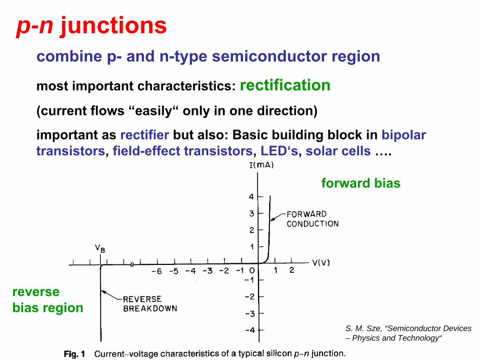
p-n junctionscombine p- and n-type semiconductor region
most important characteristics: rectification(current flows “easily“ only in one direction)
important as rectifier but also: Basic building block in bipolar transistors, field-effect transistors, LED‘s, solar cells ….
forward bias
reversebias region
S. M. Sze, “Semiconductor Devices– Physics and Technology“
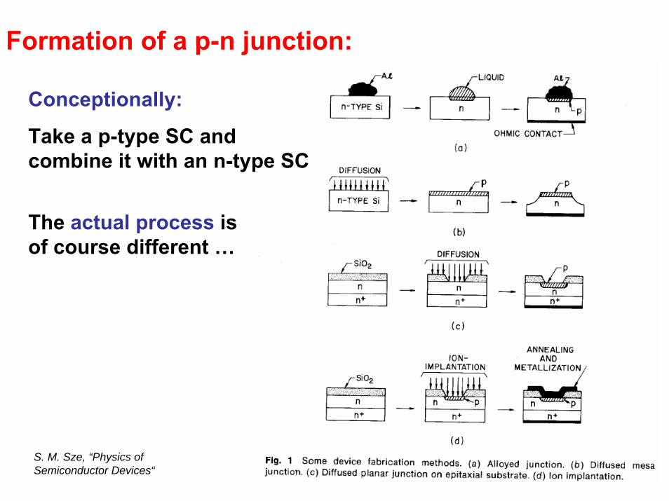
Formation of a p-n junction:
Conceptionally:
Take a p-type SC and combine it with an n-type SC
The actual process isof course different …
S. M. Sze, “Physics of Semiconductor Devices“
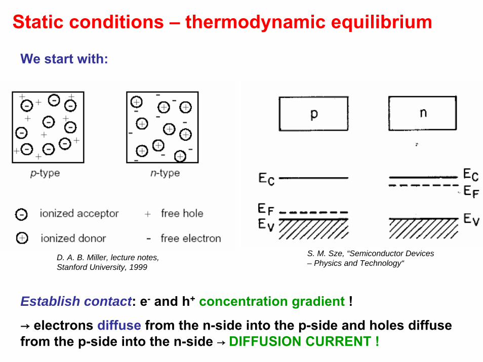
Static conditions – thermodynamic equilibrium
We start with:
S. M. Sze, “Semiconductor Devices– Physics and Technology“
D. A. B. Miller, lecture notes, Stanford University, 1999
Establish contact: e- and h+ concentration gradient !
→ electrons diffuse from the n-side into the p-side and holes diffuse from the p-side into the n-side → DIFFUSION CURRENT !
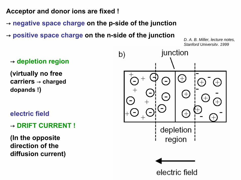
Acceptor and donor ions are fixed !
→ negative space charge on the p-side of the junction
→ positive space charge on the n-side of the junctionD. A. B. Miller, lecture notes, Stanford University, 1999
→ depletion region
(virtually no freecarriers → charged dopands !)
electric field
→ DRIFT CURRENT !
(In the oppositedirection of thediffusion current)
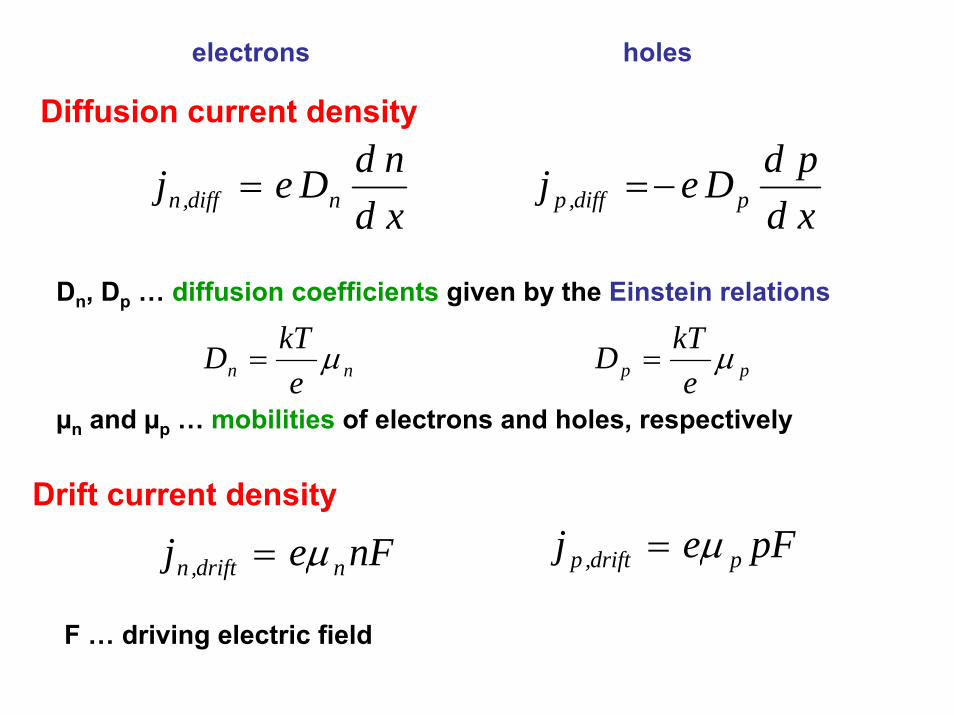
electrons holes
Diffusion current density
xdndDej ndiff,n =
xdpdDej pdiff,p −=
Dn, Dp … diffusion coefficients given by the Einstein relations
nn ekTD µ= pp e
kTD µ=
µn and µp … mobilities of electrons and holes, respectively
Drift current densitypFej pdrift,p µ=nFej ndrift,n µ=
F … driving electric field
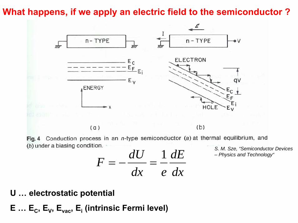
What happens, if we apply an electric field to the semiconductor ?
dxdE
edxdUF 1
=−=S. M. Sze, “Semiconductor Devices– Physics and Technology“
U … electrostatic potential
E … EC, EV, Evac, Ei (intrinsic Fermi level)
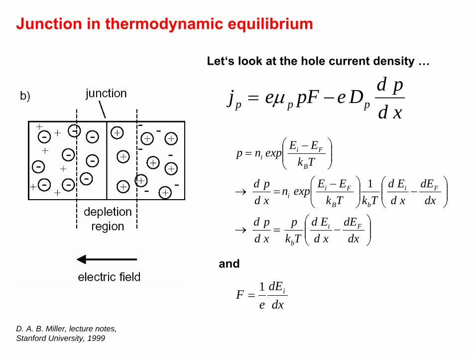
Junction in thermodynamic equilibrium
Let‘s look at the hole current density …
xdpdDepFej ppp −= µ
⎟⎟⎠
⎞⎜⎜⎝
⎛−=→
⎟⎟⎠
⎞⎜⎜⎝
⎛−⎟⎟
⎠
⎞⎜⎜⎝
⎛ −=→
⎟⎟⎠
⎞⎜⎜⎝
⎛ −=
dxdE
xdEd
Tkp
xdpd
dxdE
xdEd
TkTkEEexpn
xdpd
TkEEexpnp
Fi
b
Fi
bB
Fii
B
Fii
1
and
dxdE
eF i1=
D. A. B. Miller, lecture notes, Stanford University, 1999
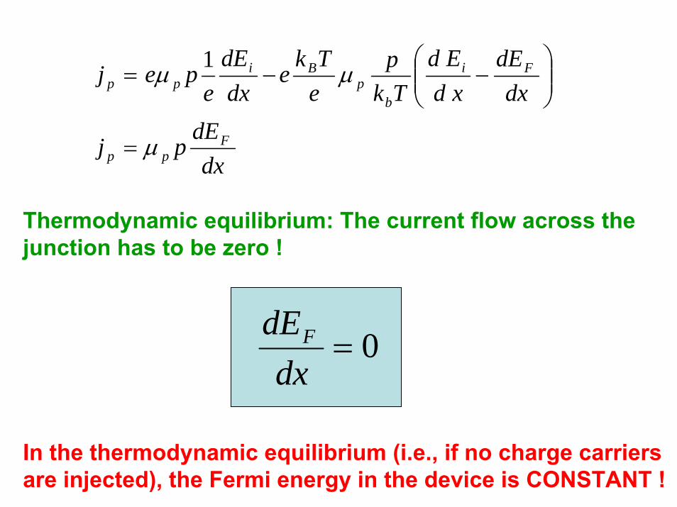
dxdEpj
dxdE
xdEd
Tkp
eTke
dxdE
epej
Fpp
Fi
bp
Bipp
µ
µµ
=
⎟⎟⎠
⎞⎜⎜⎝
⎛−−=
1
Thermodynamic equilibrium: The current flow across thejunction has to be zero !
0=dx
dEF
In the thermodynamic equilibrium (i.e., if no charge carriersare injected), the Fermi energy in the device is CONSTANT !
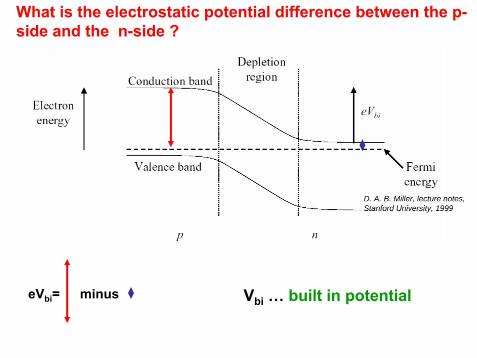
What is the electrostatic potential difference between the p-side and the n-side ?
D. A. B. Miller, lecture notes, Stanford University, 1999
Vbi … built in potentialeVbi= minus
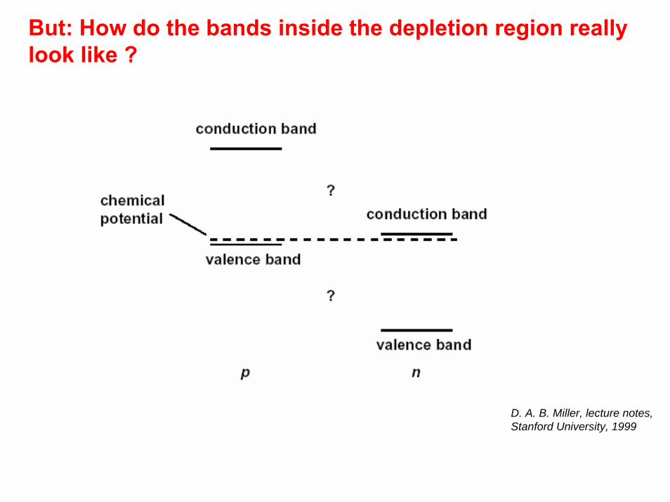
But: How do the bands inside the depletion region reallylook like ?
D. A. B. Miller, lecture notes, Stanford University, 1999
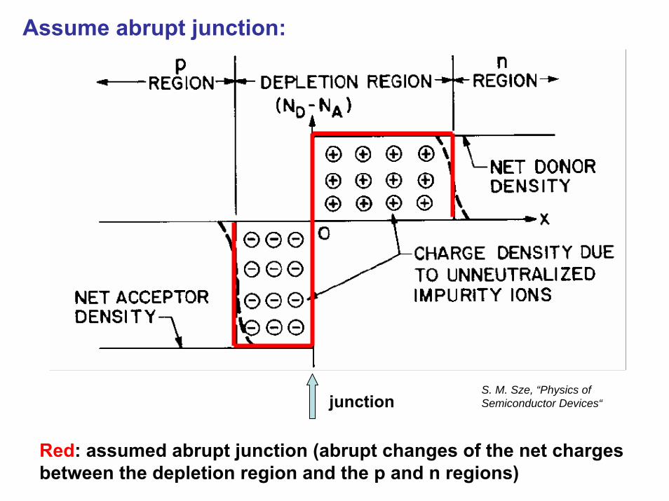
Assume abrupt junction:
S. M. Sze, “Physics of Semiconductor Devices“junction
Red: assumed abrupt junction (abrupt changes of the net chargesbetween the depletion region and the p and n regions)
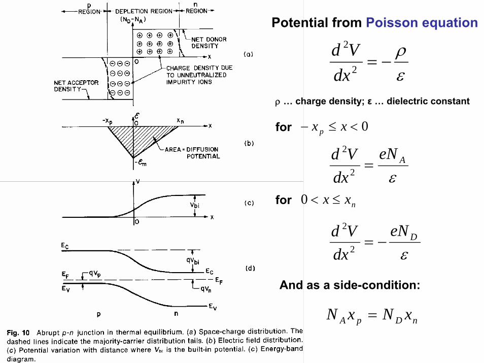
Potential from Poisson equation
ερ
−=2
2
dxVd
ρ … charge density; ε … dielectric constant
0<≤− xxpfor
nxx ≤<0for
εAeN
dxVd
=2
2
εDeN
dxVd
−=2
2
And as a side-condition:
nDpA xNxN =
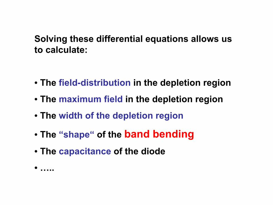
Solving these differential equations allows usto calculate:
• The field-distribution in the depletion region
• The maximum field in the depletion region
• The width of the depletion region
• The “shape“ of the band bending• The capacitance of the diode
• …..
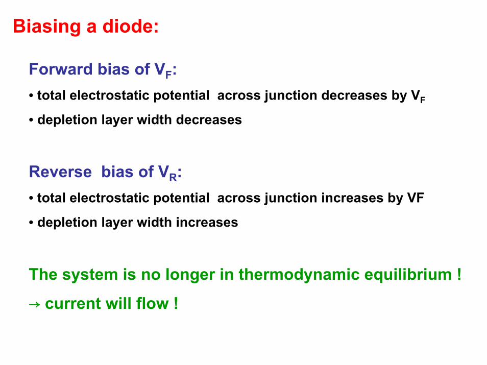
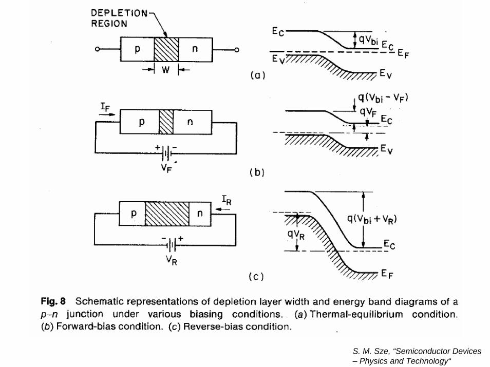
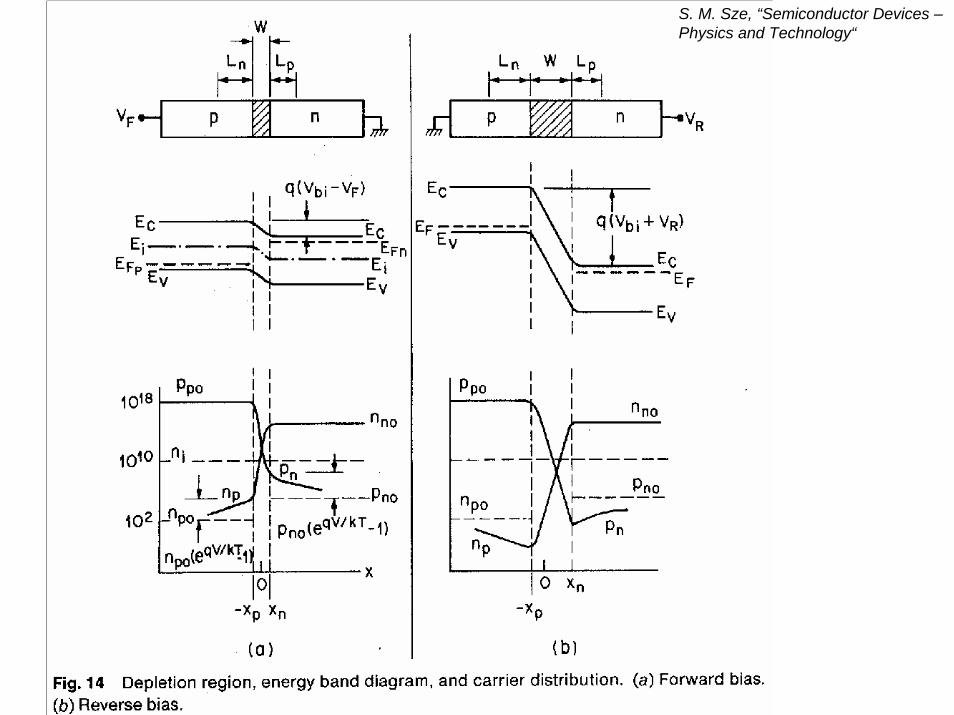
Biasing a diode:
Forward bias of VF:• total electrostatic potential across junction decreases by VF
• depletion layer width decreases
Reverse bias of VR:• total electrostatic potential across junction increases by VF
• depletion layer width increases
The system is no longer in thermodynamic equilibrium !
→ current will flow !
S. M. Sze, “Semiconductor Devices– Physics and Technology“
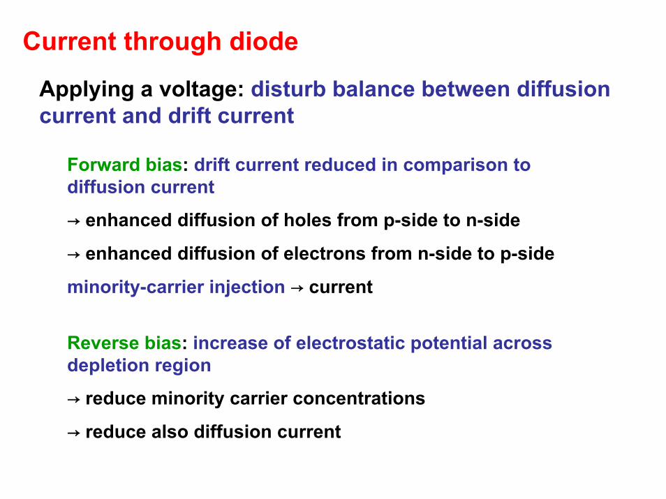
Current through diode
Applying a voltage: disturb balance between diffusioncurrent and drift current
Forward bias: drift current reduced in comparison to diffusion current
→ enhanced diffusion of holes from p-side to n-side
→ enhanced diffusion of electrons from n-side to p-side
minority-carrier injection → current
Reverse bias: increase of electrostatic potential acrossdepletion region
→ reduce minority carrier concentrations
→ reduce also diffusion current
S. M. Sze, “Semiconductor Devices –Physics and Technology“
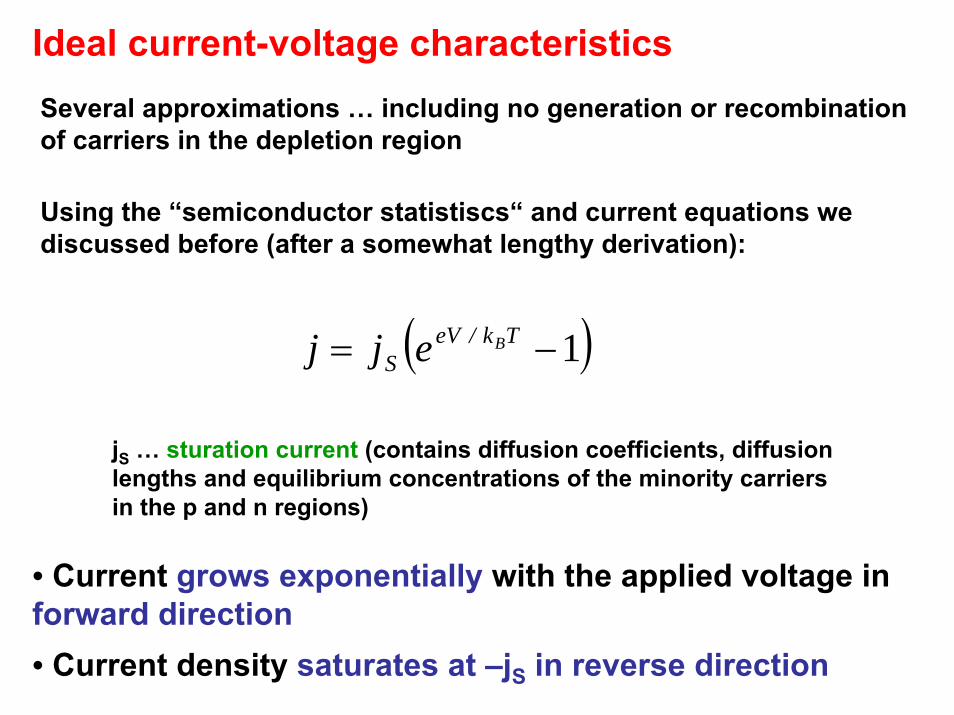
Ideal current-voltage characteristicsSeveral approximations … including no generation or recombinationof carriers in the depletion region
Using the “semiconductor statistiscs“ and current equations wediscussed before (after a somewhat lengthy derivation):
( )1−= Tk/eVS
Bejj
jS … sturation current (contains diffusion coefficients, diffusionlengths and equilibrium concentrations of the minority carriersin the p and n regions)
• Current grows exponentially with the applied voltage in forward direction• Current density saturates at –jS in reverse direction
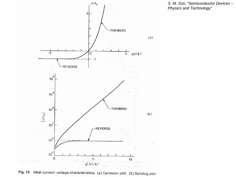
S. M. Sze, “Semiconductor Devices –Physics and Technology“
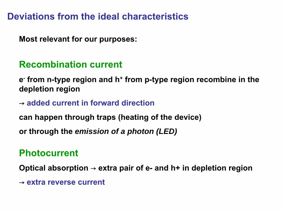
Deviations from the ideal characteristics
Most relevant for our purposes:
Recombination currente- from n-type region and h+ from p-type region recombine in thedepletion region
→ added current in forward direction
can happen through traps (heating of the device)
or through the emission of a photon (LED)
PhotocurrentOptical absorption → extra pair of e- and h+ in depletion region
→ extra reverse current
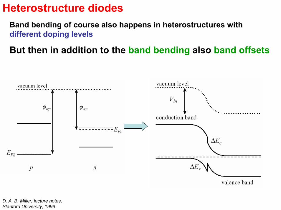
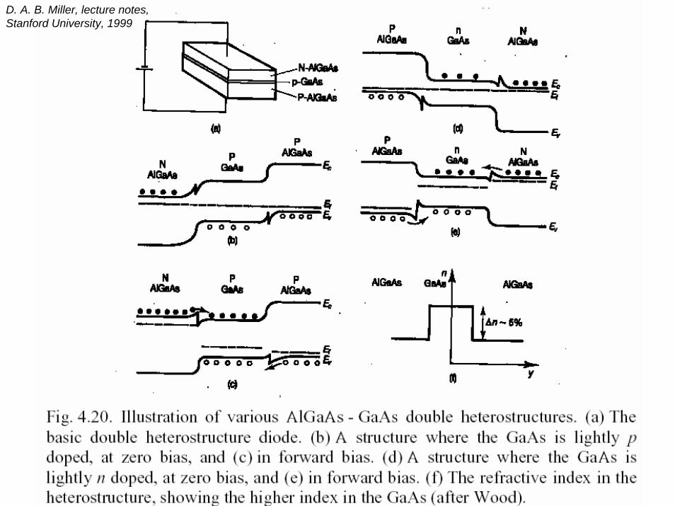
Heterostructure diodesBand bending of course also happens in heterostructures withdifferent doping levels
But then in addition to the band bending also band offsets
D. A. B. Miller, lecture notes, Stanford University, 1999
D. A. B. Miller, lecture notes, Stanford University, 1999
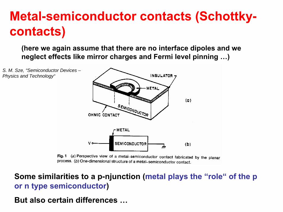
Metal-semiconductor contacts (Schottky-contacts)
(here we again assume that there are no interface dipoles and weneglect effects like mirror charges and Fermi level pinning …)
S. M. Sze, “Semiconductor Devices –Physics and Technology“
Some similarities to a p-njunction (metal plays the “role“ of the p or n type semiconductor)
But also certain differences …
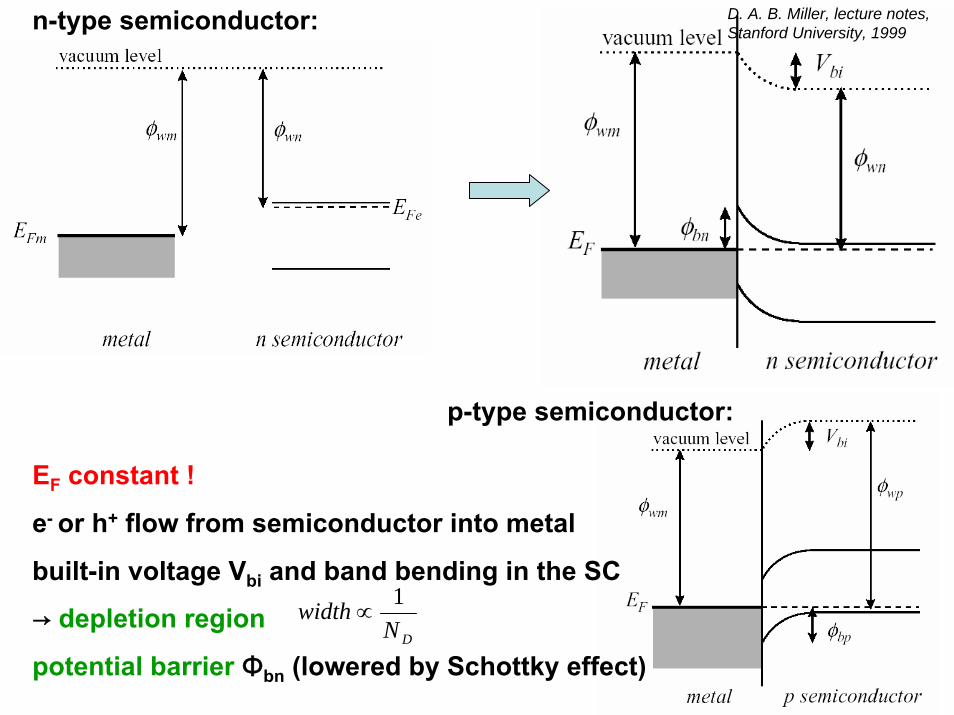
D. A. B. Miller, lecture notes, Stanford University, 1999n-type semiconductor:
p-type semiconductor:
EF constant !
e- or h+ flow from semiconductor into metal
built-in voltage Vbi and band bending in the SC
→ depletion region
potential barrier Φbn (lowered by Schottky effect)DN
width 1∝
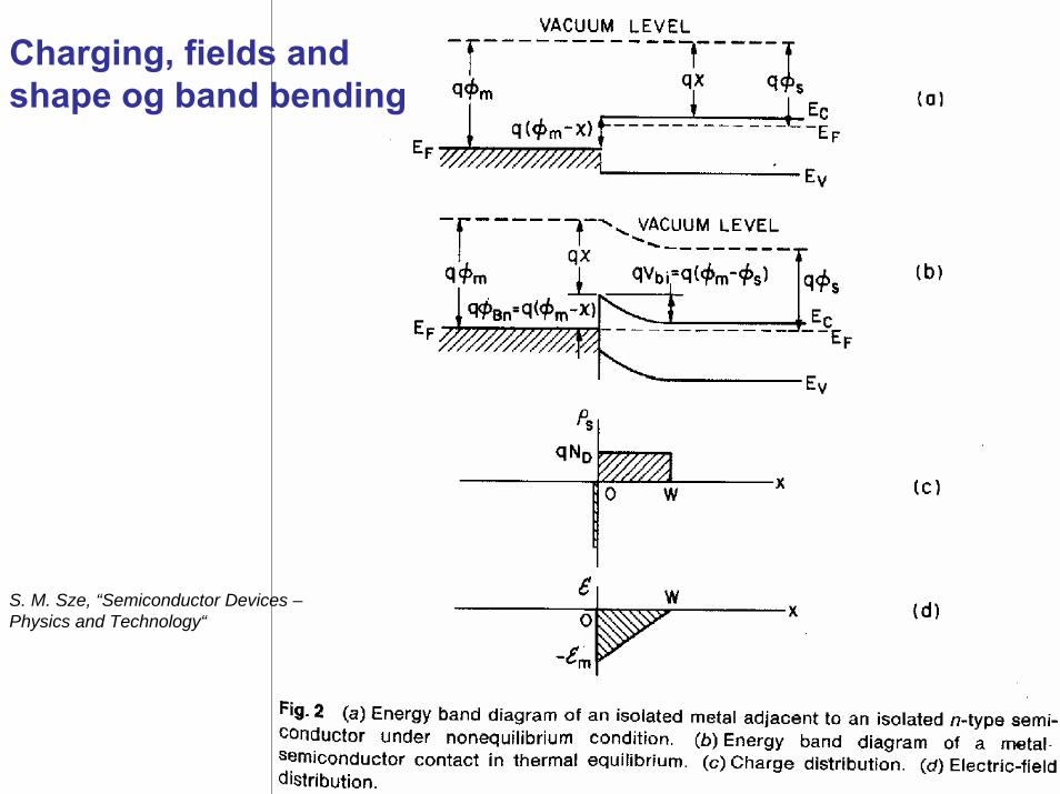
Charging, fields and shape og band bending
S. M. Sze, “Semiconductor Devices –Physics and Technology“
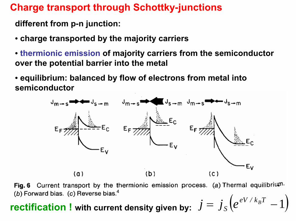
Charge transport through Schottky-junctionsdifferent from p-n junction:
• charge transported by the majority carriers
• thermionic emission of majority carriers from the semiconductorover the potential barrier into the metal
• equilibrium: balanced by flow of electrons from metal intosemiconductor
rectification ! with current density given by: ( )1−= Tk/eVS
Bejj
Ohmic contact:
Definition: metal-semiconductor contact with “negligible“contact resistance
How can this be realized ?
very high doping of the semiconductor
→ depletion region extremely short
→ e- and h+ can “easily” tunnel through resulting very thin barrier
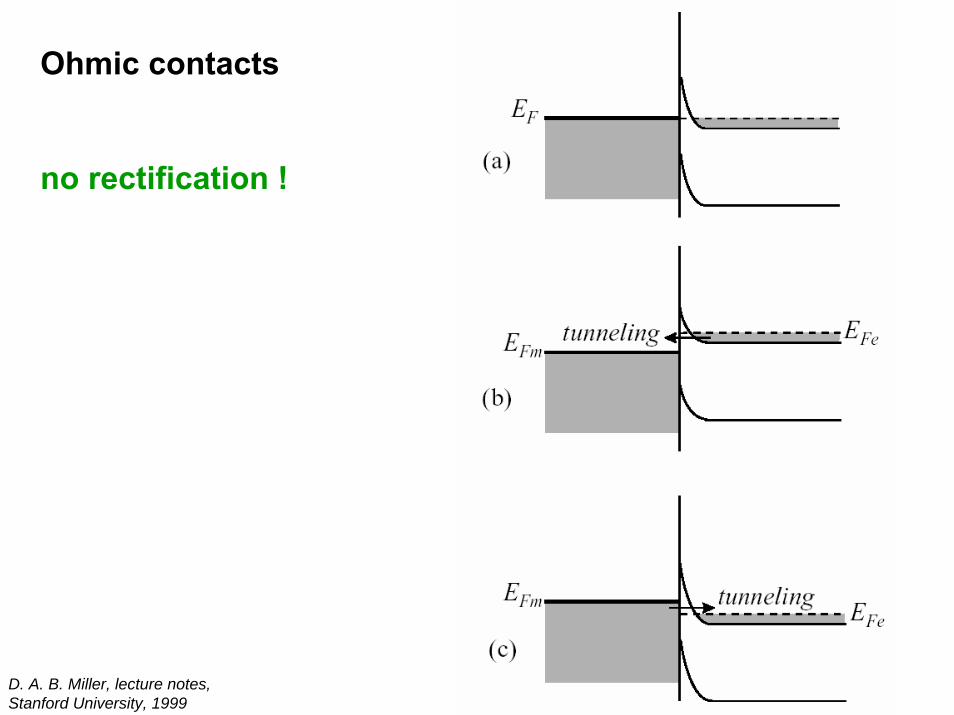
Ohmic contacts
no rectification !
D. A. B. Miller, lecture notes, Stanford University, 1999