Embed Size (px)
Citation preview
ANNO ACCADEMICO 2008 - 2009
UNIVERSITÀ DEGLI STUDI DI TRIESTE
SEDE AMMINISTRATIVA DEL DOTTORATO DI RICERCA
XXII CICLO
DEL DOTTORATO DI RICERCA IN
NANOTECNOLOGIE
Oxidation of supported PtRh particles:
size and morphology effects
(SSD FIS/03 – Fisica della Materia)
DOTTORANDO DIRETTORE DELLA SCUOLA
Matteo Maria Dalmiglio Chiar.mo Prof. Maurizio Fermeglia
(Università degli Studi di Trieste)
RELATORE Dr. Luca Gregoratti
(Sincrotrone Trieste S.C.p.A.)


Volentieri
Abstract
iii
Abstract
The chemical transformations of supported PtRh particles ranging in size from a few
micrometers to a few nanometres, and nanocrystalline films have been studied under
identical oxidizing conditions by means of different chemical and structural
characterization techniques; in particular the main technique used has been the scanning
photoemission spectromicroscopy (SPEM) available at the EscaMicroscopy beamline of
the Elettra Synchrotron Light Source. This novel experimental technique allows
sample’s chemical mapping with a spatial resolution of 100nm and the acquisition of
photoemission spectra on regions with the same dimension, and allow us to determine
the chemical state of single micro-particles. In particular we studied PtRh cluster
deposited by PLD (pulsed laser deposition) on a tungsten single crystal (W(110))
covered by a thin magnesium oxide film (MgO).
Significant variations of the Pt and Rh atoms reactivity have been revealed by
comparing the oxidation states of particles with different dimensions and, for the
micron-scale particles, also within the same island.
It was demonstrated that a selected oxidation occurs: rhodium atoms undergo stronger
and faster oxidation than platinum ones. Furthermore, the oxidation process is
composed by many intermediate steps, in which metastable oxides are formed. Very
small cluster’s oxidation (<10nm diameter) is significantly faster then the bigger one
(>100nm). Some morphological and structural clusters’ modifications after long
oxidation treatments were also investigated using a high resolution SEM (<2nm lateral
resolution).
Other measurements have been performed by using a Low Energy Electron Microscope
(LEEM) that combines a high spatial resolution (<5nm) to a high sensitivity to surface
structural modifications. In particular the behaviour of the clusters’ polycrystalline
structure has been studied during oxidation-reduction treatments. It has been shown that
the clusters’ surface is polycrystalline and that each nano crystals have different
crystallographic orientation. After oxidation each nano-crystal undergoes a different
oxidation rate. The diffraction pattern revealed that after a long oxidation the long range
order of the particles’ surface is completely lost.

Abstract
iv
A characterization of the reactivity of the PtRh particles towards oxidation after an
“ageing” process based on the repetition of many redox cycles has revealed a change in
the stability of the oxides.
Other experiments have been realized with SEM and EDX for studying the clusters’
morphology at different annealing temperatures. The results have shown structural,
chemical and morphology changes.

Abstract
v
Sommario
In questa tesi tramite diverse tecniche di caratterizzazione chimica e strutturale sono
state studiate le trasformazioni chimiche di particelle di platino-rodio (PtRh), di
dimensioni variabili tra pochi nanometri e pochi micron, e di film nano cristallini,
durante processi di ossidazione. In particolare la tecnica di analisi principale è stata
quella della spettroscopia a scansione in fotoemissione (SPEM) che è disponibile sulla
beamline EscaMicroscopy nel laboratorio di luce di sincrotrone Elettra. Questa tecnica
sperimentale permette di mappare la superficie di un campione con una risoluzione
spaziale di 100nm e di acquisire spettri di fotoemissione su regioni con le stesse
dimensioni, permettendo di determinare lo stato chimico di singole micro particelle.
In particolare abbiamo studiato le proprietà di ossidazione di cluster di PtRh depositati
mediante PLD (pulsed laser deposition) su un cristallo singolo di tungsteno (W(110))
ricoperto da un sottile film di ossido di magnesio (MgO).
Comparando gli stati di ossidazione di particelle con differenti dimensioni si sono
rilevate significative variazioni di reattività per gli atomi di Pt e di Rh e, per le particelle
di dimensioni micrometriche, si è visto che tali variazioni avvengono anche all’interno
della stessa particella.
Si è dimostrato che avviene un’ossidazione selettiva: gli atomi di rodio si ossidano
maggiormente e più velocemente di quelli di platino. Inoltre il processo di ossidazione è
composto da molti passaggi intermedi in cui si formano ossidi metastabili.
L’ossidazione di cluster più piccoli (con un diametro minore di 10nm) è
significativamente più veloce di quelli più grandi (>100nm).
Tramite l’uso di un microscopio elettronico a scansione (SEM) ad alta risoluzione
(risoluzione laterale inferiore ai 2 nm) sono state studiate alcune modifiche
morfologiche e strutturali dopo lunghi trattamenti di ossidazione.
Altre misure sono state effettuate sulla beamline Nanospectroscopy usando un Low
Energy Electron Microscope (LEEM) che unisce un’alta risoluzione spaziale (<5nm)
con un’alta sensibilità alle modifiche strutturali di superficie. Si è evidenziato come i
cluster presentino una superficie policristallina dove l’orientazione dei vari nanocristalli
è diversa da zona a zona e come i vari cristalli vadano incontro a diversi stati di

Abstract
vi
ossidazione. In particolare analizzando i pattern di diffrazione abbiamo osservato che
dopo una lunga ossidazione si perdono completamente le informazioni sulla struttura
atomica ordinata della superficie presente invece sulle particelle ridotte.
È stata effettuata una caratterizzazione della reattività di particelle di PtRh dopo un
processo di invecchiamento basato sulla ripetizione di diversi cicli di ossido-riduzione
che ha rivelato un cambiamento nella stabilità degli ossidi formati: a parità di
ossidazione le particelle “invecchiate” si riducono molto più facilmente.
Sono stati effettuati altri esperimenti atti a caratterizzare la morfologia e il
comportamento ad alte temperature dei cluster mediante l’ausilio di un microscopio
SEM e di un sistema EDX (Energy dispersive X-ray spectroscopy) ad esso
equipaggiato. Si è visto come prolungati trattamenti termici modificano la chimica, la
struttura e la morfologia superficiale delle diverse facce che costituiscono i cluster.

Contents
vii
Contents 1. Introduction 1
2. Experimental techniques used for the preparation and characterization of the
samples 8
2.1. Photoemission and Synchrotron radiation .......................................................... 8
2.1.1. Principles of Photoemission.................................................................. 8
2.1.2. Synchrotron radiation.......................................................................... 11
2.1.3. The Elettra Synchrotron Light Source ................................................ 13
2.2. The Scanning PhotoElectron Microscope (SPEM)........................................... 14
2.2.1. The SPEM Microscope at the ESCAmicroscopy Beamline at Elettra 16
2.2.2. Hemispherical Electron Analyzer and Detectors ................................ 17
2.2.3. Multichannel Detection: Spectra and Detectors.................................. 19
2.3. Low Energy Electron Diffraction (LEED) ....................................................... 21
2.4. Low Energy Electron Microscope (LEEM)...................................................... 23
2.4.1. LEEM setup ........................................................................................ 23
2.4.2. LEEM methods ................................................................................... 24
2.5. Pulsed Laser Deposition (PLD) technique........................................................ 26
2.6. Other Techniques of Surface Science used: AES, SEM and EDX................... 29
2.7. Micro Wave Plasma source .............................................................................. 32
3. Sample preparation and characterization 36
4. Oxidation states of single particles monitored by SPEM 44
4.1. Working conditions........................................................................................... 44
4.2. Results ............................................................................................................. 44
5. Structural changes evidenced by LEEM and µµµµ-LEED 56

Contents
viii
6. Other results 63
6.1. Bulk-surface stoichiometry............................................................................... 63
6.1.1. PE and EDX measurements ................................................................ 63
6.2. Morphological changes by annealing ............................................................... 65
6.2.1. Evolution of the morphology analyzed by SEM................................. 65
6.2.2. Stoichiometry after annealing ............................................................. 70
6.3. Photon Beam Induced Reduction...................................................................... 71
6.3.1. Ageing effects after redox cycles........................................................ 71
6.4. Partial coverage of a single multi-wall carbon nanotube.................................. 73
6.4.1. Carbon Nanotubes (CNTs).................................................................. 73
6.4.2. Experimental setups for the partial coverage of a single MWCN ...... 75
6.4.3. Deposition of PtRh clusters on MWCNTs.......................................... 77
7. Conclusions ............................................................................................................. 80

Chapter 1 - Introduction
1
Chapter 1
Introduction
A chemical reaction is a process in which one or more species, the reactants, undergo a
transformation to become new species called products. A special class of chemical
reactions is formed by the activated processes, for which the chemical transformation
requires a supplied energy to start.
This energy is supplied by catalysts: a catalyst is a substance that transforms reactants
into products, through an uninterrupted repeated cycle of elementary steps in which the
catalyst participates while being regenerated in its original form at the end of each
cycle. The catalyst’s activity represents the number of revolutions of the cycle per unit
time (turnover rate).
This is possible because a catalyst forms bonds with reactants, thus allowing these to
react and give rise to products while leaving the catalyst in its original form. In this way
it is possible to offer a more complex but at the same time energetically favourable and
more rapid path to final products, reducing the activation energy of the process, hence
resulting in an increased reaction rate. The catalyst does not modify the
thermodynamics of a system but acts on its kinetics.
Catalysis can be classified into three main classes. In bio-catalysis, reactions involve
biological species and enzymes play the role of catalysts. In homogeneous catalysis the
reactants and the catalyst are in the same physical state. In heterogeneous catalysis,
catalysts are in solid state and favour the reactions of species in liquid or gas phase. The
experiments reported in this thesis deal with the latter class.
The importance of heterogeneous catalysis in chemical and related industries is well
known. Approximately 90% of all chemical industry products are made using catalytic
processes [1, 2, 3]. Catalysts play also a crucial role in the abatement of environmental

Chapter 1 - Introduction
2
pollution in automotive and industrial exhausts. They are essential in the development
of efficient fuel cells, where hydrogen has become a potential idea fuel for the future.
Their importance therefore justifies the intense ongoing research efforts in this field and
in finding more stringent requirements for less expensive and more efficient catalysts.
Despite its importance in so many different and fundamental processes, explanations of
many of the phenomena involved in catalysis are still lacking, thus providing significant
motivation for fundamental research in this field. This is due to the considerable
chemical and structural complexity, mainly in the size and the structure, of real catalysts
which are usually powders, composed of transition metal (TM) nanoparticles supported
by oxide layers. These nanoparticles expose different facets, as well as defects like
steps, kinks or missing atoms, which are considered to be the most reactive sites.
On real catalysts there are different active sites and their properties arise from the
interplay of many different effects: the size of active particles, the interaction between
particles and support, the surface morphology of active materials Thus, understanding
the relation between surface heterogeneity, morphology, and chemical reactivity will
provide us with key insight into what researchers in catalysis call “selectivity”[4] i.e. the
amount of a desired product obtained per amount of consumed reactant.
When characterizing a particular measurable quantity (for example, the chemical
reactivity of the catalyst) it is not possible to disentangle the different contributions in a
direct way: in this correlation of causes lies the “complexity” of real catalysts. One
possible way to overcome some of this complexity is to study so-called model systems.
Model systems are physical systems that are simpler to understand than real catalysts,
but that can be manipulated by experimentalists in order to determine which of their
features is responsible for their chemical properties.
The fabrication of model catalysts in the context of this work requires the growth of flat,
thin, crystalline, metal oxide films on a metal single crystal surface. Metallic or oxidic
nanoparticles are deposited subsequently. A typical model is shown in Fig 1.1: a
metallic single crystal is used as a substrate for a thin oxide film, over which
nanoparticles are deposited as the active phase.
The presence of a metal oxide film is due to the fact that in a catalyst, a catalytically
active component, such as a transition metal, is dispersed over a suitable support
material —usually an oxide like alumina or silica. In the first place, this is done in order
to achieve the highest possible surface area of the active phase.

Chapter 1 - Introduction
3
Figure 1.1: Schematic of a typical surface science compatible model catalyst. Within this work, the supported particles are PtRh clusters produced by PLD
There is still only very limited fundamental knowledge about the relationship and the
interplay between structure, adsorption behaviour, and chemical or catalytic activity of
small deposited metal aggregates. It is a well known fact and the basis of many of
today’s technological applications that the catalytic properties of alloys are often
superior to those of pure metals and they have found broad applications in many
industrial processes of synthesis and exhaust gas converters [5]
When exploring the behavior of the alloys it has been shown that the individual metal
atoms generally maintain their properties, and the ligand effects due to alloying usually
result in modifications that should improve the catalyst efficiency [6, 7]. The ligand
effect represents the modification of the adsorptive properties of a given site via
electronic effects by the neighbours (ligands) of an atom that a given adsorbate binds to;
it is also related to the notion of chemical bonding and plays an important role in the
chemistry of molecules [7]. In order to identify the proper alloys that will show superior
catalytic behaviour for specific reactions it is necessary to understand the electronic
structure [8].
A textbook example in this respect is the PtRh alloy, one of the most efficient
automobile gas converter catalysts, and recently also considered as promising
electrocatalyst for use in fuel cells [9].

Chapter 1 - Introduction
4
Figure 1.2: Elements periodic table. Pt and Rh are highlighted.
In this alloy the individual Pt metal is the most active in CO oxidation, whereas Rh adds
the needed high activity for NO reduction to N2. Despite the well known efficiency of
this alloy at high temperature, e.g. steady-state automotive catalytic converters which
operate above 700°C, still its behaviour at lower temperatures, present for instance in
the cold-start emissions for automobiles or in fuel cells, has to be deeply delved [10].
Surface science compatible model catalysis suffers from two drawbacks: the pressure
gap, and the materials gap. The term “pressure gap” refers to the fact that the pressure
regime under which surface science experiments are carried out, differs from the
industrial application by several orders of magnitude. The issue that the models consist
of thin films, which are novel materials specifically created for these studies, and that
their structural and electronic properties might not be comparable to the corresponding
industrial catalyst, is summarized as the “material gap”.
The basic knowledge for the catalytic properties of the individual metals in the PtRh
alloy in oxidation/reduction reaction is provided by studies with model systems
following a bottom-up approach aimed at bridging this “material gap” between model
and real supported catalysts.
These systems are with increasing complexity and include Pt and Rh single crystal,
vicinal and highly defective surfaces, as well supported micro- and nano-particles. The
studies of single crystal and vicinal and defective surface have already provided a

Chapter 1 - Introduction
5
detailed picture of the oxygen-related adsorption, transient surface oxide and bulk oxide
structures, including the strong effects of the surface morphology, in particular the
presence of under-coordinated atoms at the vicinal and defective surfaces [11, 12].
Under oxidation conditions the structure of the initial metal plane can undergo drastic
changes, e.g. oxide formation on Pt(110) can result in a disordered phase [13]
Bimetallic systems have an increased complexity, since they have another variable, the
local organization of the two metals and the actual surface composition, which is
strongly dependent on the gas environment and temperature. In the recent report it has
been evidenced that due to the presence of different species there is a complex balance
between the energetic terms which determine the catalytically active surface
composition of PtRh bimetallic catalysts under oxidation-reduction reaction conditions
[12].
The effect of surface structure and composition becomes less predictable with
decreasing dimensionality, as evidenced by the studies of model supported metal
particles of different size and shape [14, 15]. Even in such model systems the particles
are not identical and due to geometric or electronic reasons they may behave as
individual micro-reactors, differing with respect to their catalytic activity and/or
selectivity. Recent in-situ X-ray photoelectron spectroscopy (XPS) studies comparing
the CO oxidation on Rh nano-particles of different sizes showed increased oxide
formation over smaller particles and correlated to that higher catalytic activity [16].
These findings, based on using a combination of microscopic and spectroscopic
methods for exploring the local surface composition and structure, are concomitant with
the size distribution in real catalyst particles, containing appreciable number of
coordinatively unsaturated surface atoms, which can promote surface stress and
elevated atomic mobility [17]. For the majority of catalyst particles, being in sub-10 nm
range, quantum size and support interfacial effects can play important role as well. For
the particular case of the PtRh bimetallic particles a large number of electron
microscopy and x-ray diffraction studies have been focused on looking for correlations
between their morphology, structure and catalytic activity in specific reactions,
considering only the particles bulk composition determined by the preparation
procedures [9, 18, 19]. Thermodynamic calculations and a limited number of XPS
studies have indicated similar temperature and gas adsorption effects on the surface
composition, as observed, for instance, with single crystal surfaces [19, 20]. Most of the
studies of alloy particles with different Pt and Rh weight have reached the consensus

Chapter 1 - Introduction
6
that before being exposed to reactive gases the outer shell is enriched with Pt [18], with
exception of one case reporting Rh enrichment of the surface after exposure to hydrogen
[21]. Similar dynamic response behaviour has recently been reported for bimetallic
RhPd and PtPd nanoparticle catalysts, which undergo structural and chemical changes
in response to reactive environments [8].
The present thesis work describes a synchrotron-radiation-based scanning photoelectron
microscopy (SPEM) study of a system of supported bimetallic PtRh particles. In order
to unravel the relative activity of the different PtRh particles under identical oxidizing-
reducing reaction conditions and to look for correlations with the local surface
composition evolved under the actual reaction conditions, a model system was prepared
using Pt50Rh50 target and the Pulsed Laser Deposition setup. Samples prepared with this
procedure contain a great variety of particles with different size and shape. In this way it
is possible to investigate the catalytic properties in function of the different size and of
their complex morphology and structure.
Carbon nanotubes (CNT) are a fascinating material due to their unique properties and
potential application as supporting material building block of modern nanodevices;
moreover the metal–CNT interaction is a key point of the modern research since it plays
a significant role in the integration of the next generation of nanodevices. [22]. For this
reason carbon nanotubes could be considered as a novel support also for catalytic metal
particles. In the last part of this thesis few preliminary results obtained from the
deposition of PtRh clusters on multiwalled-CNT will be presented.
This thesis is organized as follows:
Chapter 2 gives a brief overview on the experimental technique used, with a particular
attention to the Scanning PhotoElectron Microscopy (SPEM).
Chapter 3 is devoted to describe the sample preparation and characterization.
Chapter 4 deals with the oxidation of the PtRh particles monitored by SPEM, while
chapter 5 is focused on the results showing the structural changes of these particles
evidenced by LEEM and µ-LEED.
Chapter 6 concerns with other results: photoemission and fluorescence measurements
aimed at the definition of the particle bulk-surface stoichiometry, morphological
changes induced by annealing, beam induced reduction of the particles and the
deposition of PtRh clusters on multiwall carbon nanotubes.
Chapter 1 - Introduction
7
References
1 Chorkendorff, J.; Niemantsverdriet, J.W.; Concepts of Modern Catalysis and Kinetics
WILEY-VCH GmbH & Co. KgaA, 2003.
2 European White Book on Fundamental Research in Materials Science,
http://www.mpg.de/english/illustrationsDocumentation/documentation/europWhiteBoo
3 Bell, A.T. Science, 2003, 299, 1688.
4 Boudart, M. In Perspectives in Catalysis; Thomas, J.M.; Zamaraev, K.I.; Eds.;
Blackwell: Oxford, 1992, p. 183.
5 Sinfelt, J.H. “Bimetallic Catalysts: Discoveries, Concepts and Applications....”,
Wiley: New York, , 1983.
6 Somorjai, G. A. Surface Chemistry and Catalysis; Wiley: New York, 1994
7 Gauthier, Y. et al, Phys.Rev.Lett. 2001, 87, 36103
8 Jòhannesson, G.H.; Bligaard, T.; Ruban, A.V.; Skriver, H.L.; Jacobsen, K.W.;
Nørskov, J.K. Phys. Rev. Lett. 2002, 88, 255506
9 Park, K.-W.; Han, D.-S.; Sung, Y.-E. J. of Power Sources 2006, 163, 82-86
10 Lyman, C.E.; Lakis, R.E.; Stenger Jr., H.G. Ultramicroscopy 1995, 58, 25-34.
11 Wouda, P.T.; Schmid, M.; Hebenstreit, W.; Varga, P. Surf. Sci. 1997, 388, 63-70
12 Baraldi, A.; Giacomello, D.; Rumiz, L.; Moretuzzo, M.; Lizzit, S.; Buatier De
Mongeot, F.; Paolucci, G.; Kiskinova, M. J. Am. Chem. Soc. 2005, 127, 5671-5674
13 Hendriksen, B.L.M.; Frenken, J.W.M. Phys. Rev.Lett. 2002, 89, 046101
14 Dudin, P.; Barinov, A.; Gregoratti, L.; Scaini, D.; He, Y.B.; Over, H.; Kiskinova, M.
J. Phys. Chem. C 2008, 112, 9040–9044
15 Libuda, J.; Freund, H.-J. Surf. Sci. Rep. 2005, 57, 157
16 Grass, E.; Y. Zhang, Y.; Butcher, D.R.; Park, J.Y.; Li, Y.; Bluhm, H.; Bratlie, K.M.;
T. Zhang, T.; Somorjai, G.A. Angew. Chemie Intern. 2008, 47, 8893
17 Ajayan, P.M.; Marks, L.D. Phys. Rev. Lett., 1989, 63, 279; Lai, S.L. et al. Phys. Rev.
Lett. 1996, 77, 99
18 Paál, Z.; Gyorffy, N.; Wootsch, A.; Tóth, L.; Bakos, I.; Szabó, S.; Wild, U.; Schlögl,
R. Z. J. of Catalysis 2007, 250, 254-263.
19 Dhepe, P.L.; Fukuoka, A.; Ichikawa, M. Phys. Chem. Chem. Phys. 2003, 5, 5565.
20 Mezey, L.Z.; Hofer, W. Surf. Sci. 1998, 402-404, 845-850
21 L. Zhu et al. J. of Catalysis 1997 167, 408-411.
22 Bittencourt, C.; Feten, A.; Douhard, B.; Ghijsen, J.; Johnson, R.L.; Drue, W.; Pireaux, J.-J. Chem. Phys. 2006, 328, 385-391.

Chapter 2 - Experimental techniques
8
Chapter 2
Experimental Techniques used for the
preparation and characterization of
the samples
2.1. Photoemission and Synchrotron radiation
Electron storage rings are now in their third generation. The fields of application for the
radiation produced by synchrotrons are extremely wide and range from surface science
to medical research. In addition, many conventional techniques have improved their
performance and have expanded their field of application by using the synchrotron
radiation. Among these, photoemission must certainly be included.
2.1.1. Principles of Photoemission
The roots of X-ray Photoelectron Spectroscopy (XPS) can be traced back to the
discovery of the photoelectric effect by Hertz, the description of its energetics by
Einstein, and to the publication of XPS spectra from several metals by Robinson and
Rawlinson [1, 2]. Siegbahn et al. [3] managed to develop XPS into a sensitive, high-
resolution method for the determination of binding energies of electrons. Today, XPS is
applied to a wide range of materials and provides information about their composition
and, to a lesser extent, bonding and structure.

Chapter 2 - Experimental techniques
9
In an XPS experiment electrons are photoionized from the core levels by X-rays. The
X-rays can be produced by conventional sources (Al and Mg anodes are the most
common sources) or by synchrotron sources.
The cornerstone of XPS is the measurement of the kinetic energy Ekin of the outgoing
electron. This energy is related to the electron binding energy Eb in this way:
samplebkin h Φ−−= EE ν (2.1)
Here hν is photon energy of the incident X-rays and Φsample is the extra-energy needed
to reach the vacuum level far away the atom; hν and Φsample are known.
Core levels
Valence band
Fermi level
Vacuum level
Ekin
ΦΦΦΦAnalyzerΦΦΦΦSample
E'kin
Sample Analyzer
Figure 2.1: Graphical description of equation (2.1)
As shown in Fig.2.1 it must be noted that in order to be detected the photoelectron
emitted with Ekin has to overcome the work function of the electron analyzer, Φanalyzer
which is typically low, and then it will be detected with an energy E'kin. Usually the
position of the Fermi level is defined as the reference level (Eb=0).
Contemporary XPS provides information about the environment of surface atoms [4].
Though core electrons are very localized and their wavefunctions are hardly affected by
the surrounding, the binding energy of a core electron depends on the charge of the
atom as well as on the background electrostatic potential in the core region. The matter
is somewhat complicated by the dependence of the binding energy on the efficiency of
Sample Analyzer

Chapter 2 - Experimental techniques
10
dielectric screening. These factors (background potential, charge and screening) are
different on the surface than in the bulk. The differences are often called Surface Core
Level Shifts (SCLS). The sign and the magnitude of the shift, which may range from
few tenths of eV to a few eV, are signatures of the local environment of a surface atom.
Screening enters into the description of the core level shifts because the electrons
ejected from the solid leave a core hole [5, 6]. The energy of this hole depends on how
efficiently its charge is screened by the electrons of the crystal, and reflects the energy
of the core electron before it is ejected (initial state approximation) or rather the energy
of the core hole (final state approximation). The answer depends on how efficiently the
other electrons can screen the hole within the time needed for the photoemission
process. If the surrounding electrons react extremely slowly, the ejected electron
escapes as in the initial state picture. If the surrounding electrons react extremely fast,
the ejected electron takes with it the whole screening energy and the final state picture
with static screening of the hole is valid. Generally the photoelectron can take only a
part of the screening energy. One should thus consider dynamical screening effects; the
energy of the photoelectron is expected to be somewhere between the limits set by the
initial state and final state approximations. In any case screening of the hole causes the
photoelectron to appear at a higher kinetic energy, reducing its measured binding
energy.
In the soft X-ray regime radiation can penetrate a few microns into condensed matter
but because of the limited escape depth of the photoelectrons (a few nanometers at such
energies), the intensity of the emitted photoelectrons is proportional to the number of
illuminated atoms typically within one escape depth of the surface. This is the basis of a
quantitative XPS analysis [7].
2.1.2. Synchrotron Radiation
The line sources of X-rays used in conventional XPS are of course discrete, and for
some type of experiments that represents a severe limitation. What is needed is a source
of adequate intensity capable of being tuned continuously over the required energy
range, and for this, a synchrotron radiation source is particularly suitable.
A synchrotron source exploits the fact that, when a charged body is accelerated it emits
radiation, a process that is particularly efficient for an electron because of its small
mass. Electrons are accelerated to relativistic velocities around an approximately
Chapter 2 - Experimental techniques
11
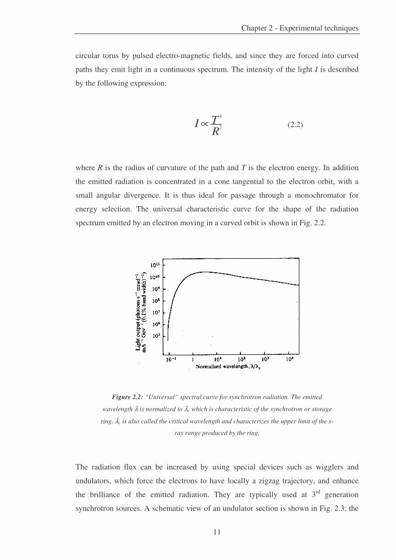
circular torus by pulsed electro-magnetic fields, and since they are forced into curved
paths they emit light in a continuous spectrum. The intensity of the light I is described
by the following expression:
I ∝4T2R
(2.2)
where R is the radius of curvature of the path and T is the electron energy. In addition
the emitted radiation is concentrated in a cone tangential to the electron orbit, with a
small angular divergence. It is thus ideal for passage through a monochromator for
energy selection. The universal characteristic curve for the shape of the radiation
spectrum emitted by an electron moving in a curved orbit is shown in Fig. 2.2.
Figure 2.2: “Universal” spectral curve for synchrotron radiation. The emitted
wavelength λ is normalized to λc which is characteristic of the synchrotron or storage
ring. λc is also called the critical wavelength and characterizes the upper limit of the x-
ray range produced by the ring.
The radiation flux can be increased by using special devices such as wigglers and
undulators, which force the electrons to have locally a zigzag trajectory, and enhance
the brilliance of the emitted radiation. They are typically used at 3rd generation
synchrotron sources. A schematic view of an undulator section is shown in Fig. 2.3; the

Chapter 2 - Experimental techniques
12
letters N and S identify the poles of the magnetic field used to deviate the trajectory of
the electrons.
Monochromator design and radiation and undulators physics are complex and
specialized and this is not the appropriate place to discuss them in detail (a complete
description of these devices can be found in Refs. 8 and 9).
Figure 2.3: Schematic picture of an undulator (or wiggler). It consists of a periodic
series of magnets, placed in a ring section where the electron path would otherwise be
straight; because of its action, the electrons are forced to wiggle around the straight
path. The result is a very high flux of X-rays along the wiggler beamline. An undulator
is similar to a wiggler except for one point: it forces the electrons into a much weaker
zigzag, so that during the entire zigzag motion synchrotron light continues to illuminate
the undulator beamline. The result is a longer pulse of light rather than a series of short
bursts. Without short pulses, there is no wide band of wavelengths, thus the undulator
emission is not spread in a wide band but concentrated, producing high levels of flux
and brightness. The picture is taken from the Elettra web site pages
(http://www.elettra.trieste.it/).
Summarizing, some advantages of synchrotron radiation are: a wide spectra range, high
photon flux, high collimation of the synchrotron light beam, spatial coherence and a
possibility to choose the degree of polarization of the light.
Chapter 2 - Experimental techniques
13
2.1.3. The Elettra Synchrotron Light Source
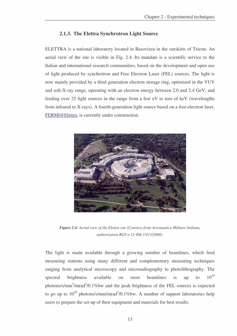
ELETTRA is a national laboratory located in Basovizza in the outskirts of Trieste. An
aerial view of the site is visible in Fig. 2.4. Its mandate is a scientific service to the
Italian and international research communities, based on the development and open use
of light produced by synchrotron and Free Electron Laser (FEL) sources. The light is
now mainly provided by a third generation electron storage ring, optimized in the VUV
and soft-X-ray range, operating with an electron energy between 2.0 and 2.4 GeV, and
feeding over 25 light sources in the range from a few eV to tens of keV (wavelengths
from infrared to X-rays). A fourth-generation light source based on a free-electron laser,
FERMI@Elettra, is currently under construction.
Figure 2.4: Aerial view of the Elettra site (Courtesy from Aeronautica Militare Italiana,
authorization RGS n.12-466 15/11/2000).
The light is made available through a growing number of beamlines, which feed
measuring stations using many different and complementary measuring techniques
ranging from analytical microscopy and microradiography to photolithography. The
spectral brightness available on most beamlines is up to 1019
photons/s/mm2/mrad2/0.1%bw and the peak brightness of the FEL sources is expected
to go up to 1030 photons/s/mm/mrad2/0.1%bw. A number of support laboratories help
users to prepare the set-up of their equipment and materials for best results.

Chapter 2 - Experimental techniques
14
Figure 2.5: Displacement of the beamlines at Elettra. The picture is taken from the
Elettra web site pages (http://www.elettra.trieste.it/).
A as we can see from Fig. 2.5 the ESCAmicroscopy beamline, as many others, shares
an insertion device, reducing the time available for measurement on each experimental
station, but on the other hand it increases the possibility to connect more beamlines to
the ring.
2.2. The Scanning PhotoElectron Microscope (SPEM)
In this part, the main features of the SPEM on the ESCAmicroscopy beamline are
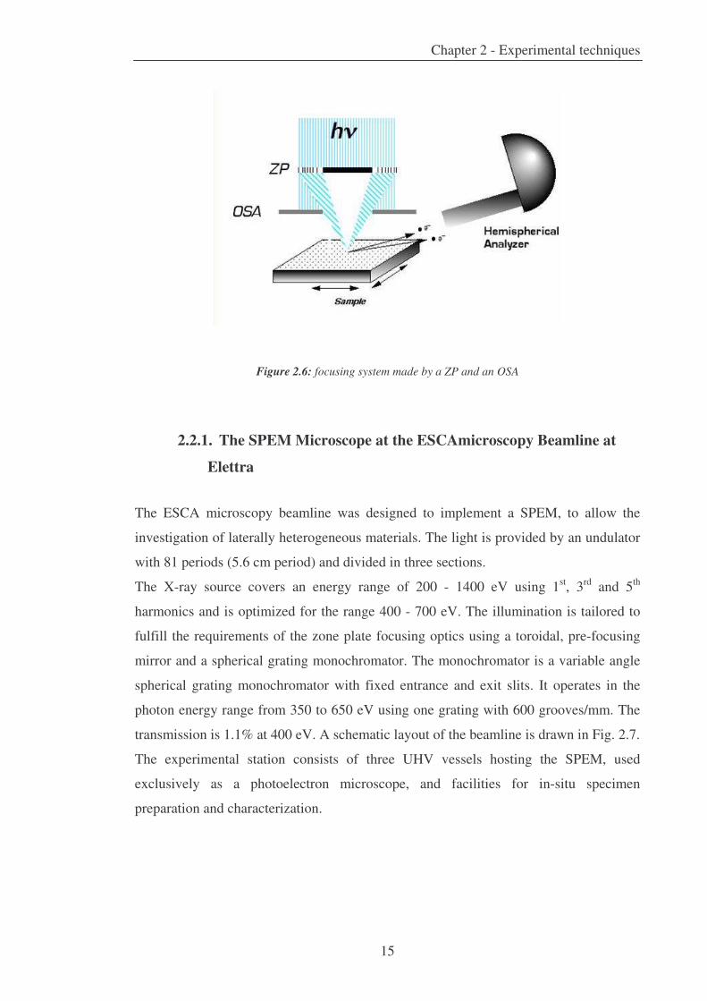
considered. The focused x-ray probe is formed using a Fresnel zone plate (Fig. 2.6), and
it is this device that crucially influences the spatial resolution that can be achieved, so it
is important to be aware of the main parameters that characterize these optical elements.
The SPEM is itself just one part of the whole experimental station: the SPEM vacuum
chamber is attached to additional vacuum chambers that provide facilities for in situ
sample preparation, and other apparatus for surface characterization, such as LEED
(Low Energy Electron Diffraction) and AES (Auger Electron Spectroscopy) detectors
(see after for a detailed description of this techniques).
Chapter 2 - Experimental techniques
15
Figure 2.6: focusing system made by a ZP and an OSA
2.2.1. The SPEM Microscope at the ESCAmicroscopy Beamline at
Elettra
The ESCA microscopy beamline was designed to implement a SPEM, to allow the
investigation of laterally heterogeneous materials. The light is provided by an undulator
with 81 periods (5.6 cm period) and divided in three sections.
The X-ray source covers an energy range of 200 - 1400 eV using 1st, 3rd and 5th
harmonics and is optimized for the range 400 - 700 eV. The illumination is tailored to
fulfill the requirements of the zone plate focusing optics using a toroidal, pre-focusing
mirror and a spherical grating monochromator. The monochromator is a variable angle
spherical grating monochromator with fixed entrance and exit slits. It operates in the
photon energy range from 350 to 650 eV using one grating with 600 grooves/mm. The
transmission is 1.1% at 400 eV. A schematic layout of the beamline is drawn in Fig. 2.7.
The experimental station consists of three UHV vessels hosting the SPEM, used
exclusively as a photoelectron microscope, and facilities for in-situ specimen
preparation and characterization.

Chapter 2 - Experimental techniques
16
Figure 2.7: Scheme of the ESCA microscopy beamline. The picture is taken from the
ESCAmicroscopy web pages inside the Elettra web site
(http://www.elettra.trieste.it/escamicroscopy).
The experimental apparatus allows the user to carry out many different experiments,
aiming at quantitative and qualitative chemical characterization of the surface of
morphologically complex natural and fabricated materials (electronic devices,
superconductors, catalysts, thin films, materials with corrosion damage, etc.), including
chemical reactions and mass transport processes leading to lateral changes in the
composition, morphology and electronic properties of materials.
The specimen is introduced through a fast entry air-lock and transported using magnetic
arms and wobble sticks. The preparation chamber includes detectors for Low Energy
Electron Diffraction (LEED), Auger Electron Spectroscopy (AES), a sputter gun, a gas
inlet system, evaporation sources and facilities for sample heating.
The SPEM microscope at Elettra allows the scanning of the sample using either stepper
or piezoelectric motors. The smallest step achievable with the stepper motors is 1
micron. The images acquired with these motors cover typically large areas (2x10⁴-
1x105 µm2) and are used for the identification of the best regions that have to be
measured. The time needed to complete one movement of one stepper motor (dead
time) is at least 150 ms, much higher than that of the piezoelectric motor which is
limited to few ms. This is the reason why most of the images during a typical
spectromicroscopy experiment at the SPEM at Elettra are acquired using the

Chapter 2 - Experimental techniques
17
piezoelectric motors. The maximum range covered by the piezoelectric motors is 64x64
µm2.
The smallest step that these motor can make is 5 nm, much smaller than the photon
beam size. A typical image has 100x100 or 200x200 pixels with counting times ranging
from 20 to 200 ms per pixel. It implies that the time spent for the acquisition of one
image ranges from a few minutes up to one hour. The piezo motors do not suffer of the
problem of backlash and then the positioning of the beam over small areas can be made
easily and precisely using them.
The SPEM has two operation modes, microspot XPS spectroscopy and spectro-imaging,
executed by monitoring the photoelectrons emitted within a selected energy window
while rastering the sample. The spectro-imaging mode allows the reconstruction of the
spectrum contained in the energy window, from micro-areas selected from the two-
dimensional maps.
The core of the detection system of any SPEM is the electron analyzer. For the
acquisition of the data presented in this thesis, the experimental station was equipped
with an Hemispherical Electron Analyzer (HEA) from SPECS (model PHOIBOS 100)
equipped with a wide angle set of electrostatic lenses and placed at 30° respect to the
sample surface. This particular geometrical configuration enhances the characteristic
surface sensitivity of the SPEM technique.
2.2.2. Hemispherical Electron Analyzer and Detectors
The HEA is the type of analyzer chosen in the earliest days of XPS as most suitable for
that technique, and it has remained so ever since. The basic form of a HEA is shown
diagrammatically in Fig. 2.8. Two hemispheres of radii R1 (inner) and R2 (outer) are
positioned concentrically. Potentials –V1 and –V2 are applied to the inner and outer
hemispheres respectively, with V2 greater than V1. The median equipotential surface
between the hemispheres has radius R0 and the source S and focus F are co-linear with
the centre of curvature.

Chapter 2 - Experimental techniques
18
Figure 2.8: Schematic cross-section of a hemispherical electron analyser. Two
hemispheres of radii R1 (inner) and R2 (outer) are positioned concentrically. R0 is the
radius of the median equipotential surface. Potentials –V1 and –V2 are applied to the
inner and outer spheres respectively, with V2 greater than V1. The source S is located in
the entrance slit of width W1 and the focus F in the exit slit of width W2. The divergence
of the electrons entering the analyser from the ideal tangential path is δα.
The potential –V0 along the median surface is:
RRVRV
V2 0
22110
+= (2.3)
If electrons of energy E=eV0 are injected tangentially to the median surface at radius R0
they will describe circular orbits of radius R0 according to the expressions:
1V = 0V 3 − 2 0R1R
� � �
� � �
�
�
� � � (2.4) 2V = 0V 3 − 2 0R
2R
� � �
� � �
�
�
� � � (2.5)
from which:
2V − 1V = 0V 2R1R
− 1R2R
� � �
� � � (2.6) e∆V = E 2R
1R− 1R
2R
� � �
� � � (2.7)
Chapter 2 - Experimental techniques
19
Electrons of the correct energy E, injected tangentially at the source S, are all focused at
F, for the complete hemisphere with radius R0, i.e. for all planes through SF out of the
plane of Fig. 2.8. If the electrons are injected at an angle δα to the correct tangential
direction and with an energy ∆E different from the correct energy E than the shift ∆R
along the radius R0 from the correct focal position is then given by:
∆R = 2 0R∆EE
− δα( )2� �
� � (2.8)
I limit this presentation to the general principles without going inside the complex
theory of the HEAs. A complete treatment of this matter together with the derivation of
the formulas cited above can be found in Ref. [7].
Electrons at the exit slit of an HEA are counted by an electron detector. The HEA of the
ESCAmicroscopy beamline was equipped with a multichannel electron detector (48-
channels) based on channel plates as the multiplier elements and developed by the
‘Unità operativa servizio rilevatori e strumentazione’ group of Elettra.
2.2.3. Multichannel Detection: Spectra and Detectors
Using a 48-channel electron detector in SPEM has reduced substantially the
measurement time necessary for the acquisition and the analysis of the images and has
provided high efficiency, allowing with a single scan the possibility to map different
chemical states and/or different elements, including the background signal as well. Fig.
2.9 shows schematically the operation of the multichannel detector. The counts
collected by each channel correspond to a specific kinetic energy defined by the kinetic
and pass energies at which the analyzer is set; the energy range covered by all the
channels is the so-called “energy window”. Thus the 48-channel image contains 48
energy–separated images. In this way problems of misalignment, drifts of the samples
or optics, short lifetime of the probed sample, etc., can be avoided.

Chapter 2 - Experimental techniques
20
Figure 2.9: Schematic view of the multichannel data acquisition; the 48-channel
images can provide both selected energy maps and 48-points spectra from selected
areas.
The 48 signal values saved for each pixel of an image can also be used to plot a
photoemission spectrum of 48 points, as illustrated in Fig. 2.9; each point corresponds
to a specific kinetic energy determined by the selected energy window. These types of
spectra are limited by the low number of points, but in special cases when the expected
energy shifts or shape of the spectra differ substantially across the surface they can be
used to extract important spectral information directly from the images.
The acquisition of the photoemission spectra with the multichannel electron detector
was performed using a scanning mode; in this mode each point of the spectrum, which
corresponds to a specific kinetic energy, is counted by each of the 48 anodes, thereby
averaging the different sensitivity of the channels. The so-called “snapshot” acquisition
mode, where each point of the spectrum is counted by only one channel and calibrated
with respect to its sensitivity, was not used due to the low number of channels available.
The gain in the acquisition time using a 48-channels detector with “snapshots” is in fact
small with respect to the normal scanning mode.

Chapter 2 - Experimental techniques
21
2.3. Low Energy Electron Diffraction (LEED)
Low-energy electron diffraction (LEED) is a technique used for the determination of the
surface structure of crystalline materials based on the bombardment with a collimated
beam of low energy electrons (20-200eV) [10] and on the observation of diffracted
electrons as spots on a fluorescent screen. The diffraction of low energy electrons from
a crystal surface was first discovered in 1927 by Davisson and Germer [11,12]. A low
voltage V accelerates the electrons towards the sample surface, were they are scattered.
If we consider an electron with a momentum p, its wave function will have the
following de Broglie wavelength [64]:
(2.9)
where h = 6.626 × 10⁻³⁴ Js is the Planck constant, m = 9.11 × 10⁻³¹ kg is the electron
mass and e = 1.6022 × 10⁻¹⁹ C is the elementary charge. According to this equation, the
typical LEED voltages, in the range 20÷200 eV, correspond therefore to wave lengths
lower than 0.3nm (i.e. of the order of interatomic distances in the crystalline sample
lattice).
As shown in Fig. 2.10, a collimated and monoenergetic beam of electrons is accelerated
towards the surface. Some of the impinging electrons are elastically scattered back
towards the electron source. The spatial distribution of the intensity maxima (LEED
pattern) of the backscattered electron stream at the electron source is determined by the
surface structure. As it turns out, the positions of the intensity maxima correspond to the
lattice structure of the surface in reciprocal space. Thus, the mere observation of a
LEED pattern yields information about the surface structure and its long range order.
Figure 2.10: schematic view of a LEED apparatus.
Chapter 2 - Experimental techniques
22
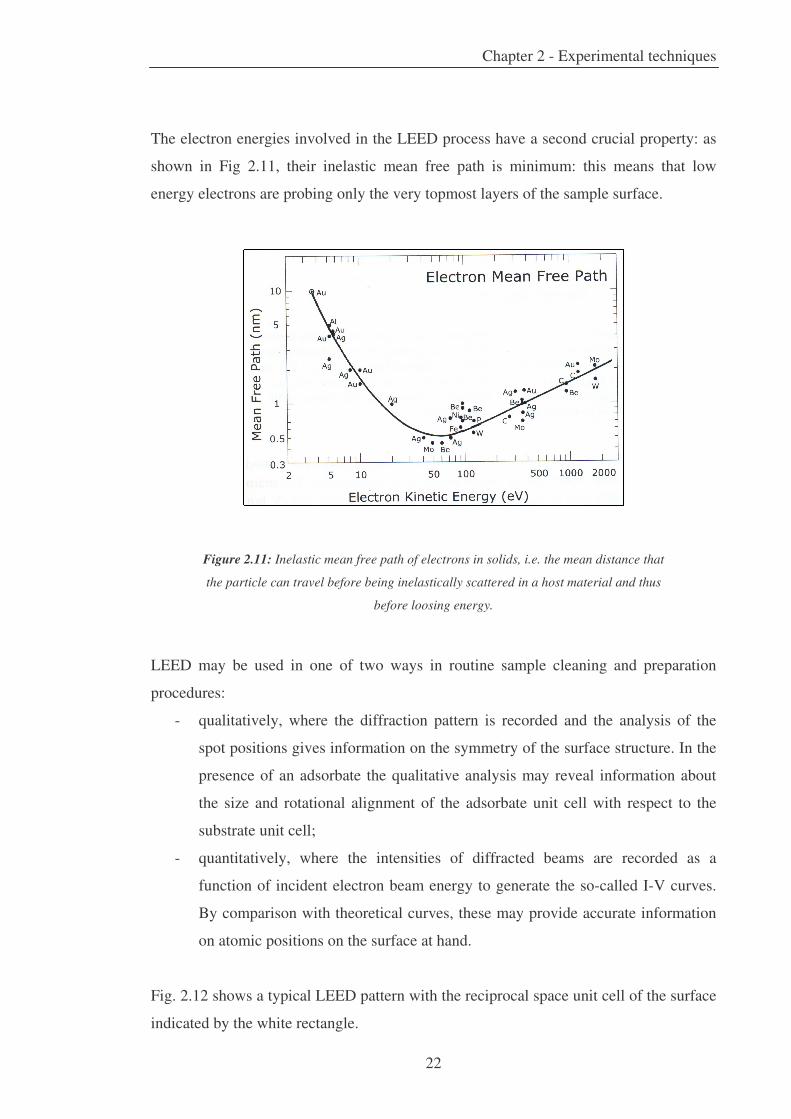
The electron energies involved in the LEED process have a second crucial property: as
shown in Fig 2.11, their inelastic mean free path is minimum: this means that low
energy electrons are probing only the very topmost layers of the sample surface.
Figure 2.11: Inelastic mean free path of electrons in solids, i.e. the mean distance that
the particle can travel before being inelastically scattered in a host material and thus
before loosing energy.
LEED may be used in one of two ways in routine sample cleaning and preparation
procedures:
- qualitatively, where the diffraction pattern is recorded and the analysis of the
spot positions gives information on the symmetry of the surface structure. In the
presence of an adsorbate the qualitative analysis may reveal information about
the size and rotational alignment of the adsorbate unit cell with respect to the
substrate unit cell;
- quantitatively, where the intensities of diffracted beams are recorded as a
function of incident electron beam energy to generate the so-called I-V curves.
By comparison with theoretical curves, these may provide accurate information
on atomic positions on the surface at hand.
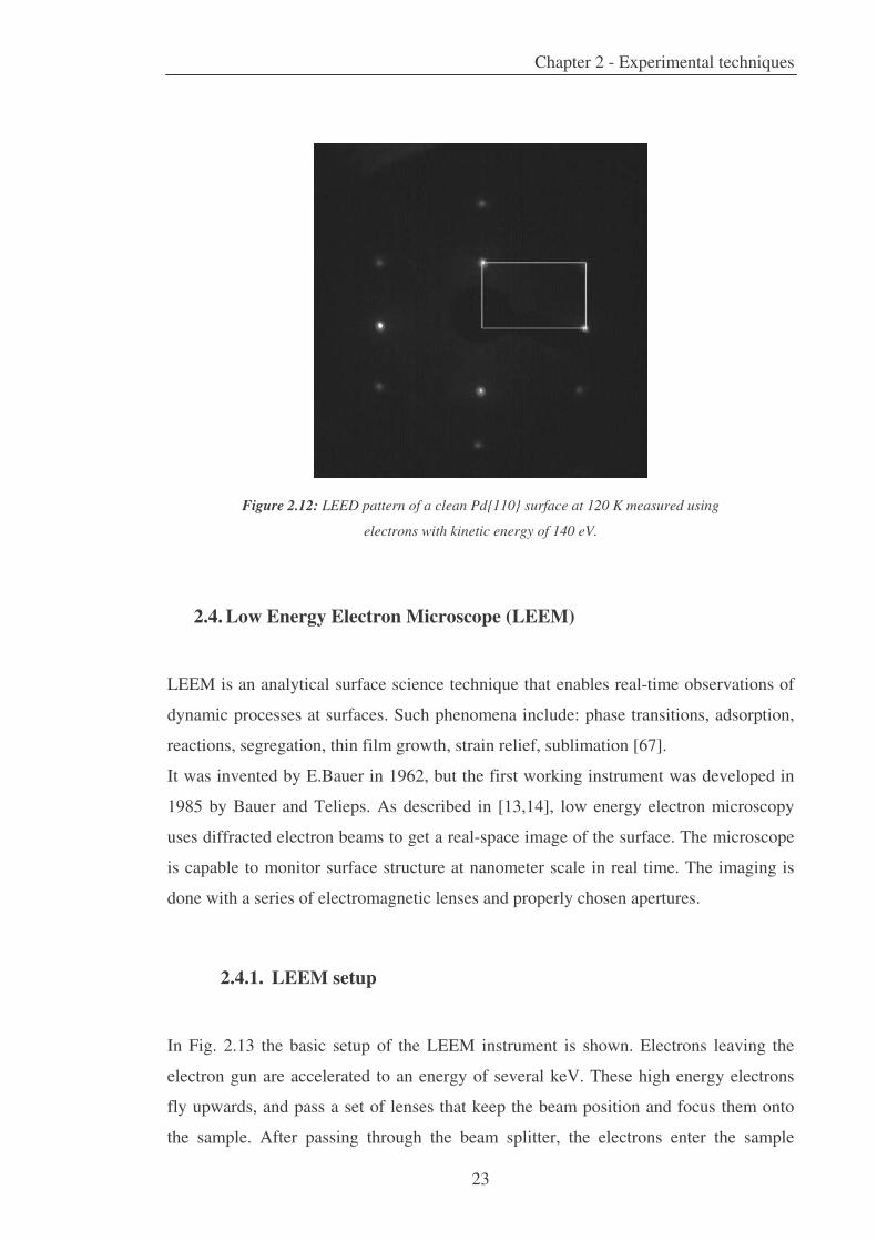
Fig. 2.12 shows a typical LEED pattern with the reciprocal space unit cell of the surface
indicated by the white rectangle.
Chapter 2 - Experimental techniques
23
Figure 2.12: LEED pattern of a clean Pd{110} surface at 120 K measured using
electrons with kinetic energy of 140 eV.
2.4. Low Energy Electron Microscope (LEEM)
LEEM is an analytical surface science technique that enables real-time observations of
dynamic processes at surfaces. Such phenomena include: phase transitions, adsorption,
reactions, segregation, thin film growth, strain relief, sublimation [67].
It was invented by E.Bauer in 1962, but the first working instrument was developed in
1985 by Bauer and Telieps. As described in [13,14], low energy electron microscopy
uses diffracted electron beams to get a real-space image of the surface. The microscope
is capable to monitor surface structure at nanometer scale in real time. The imaging is
done with a series of electromagnetic lenses and properly chosen apertures.
2.4.1. LEEM setup
In Fig. 2.13 the basic setup of the LEEM instrument is shown. Electrons leaving the
electron gun are accelerated to an energy of several keV. These high energy electrons
fly upwards, and pass a set of lenses that keep the beam position and focus them onto
the sample. After passing through the beam splitter, the electrons enter the sample

Chapter 2 - Experimental techniques
24
chamber passing through the objective lens, being decelerated to low energy (by
holding the sample at a potential close to the accelerating one). The low energy
electrons are elastically backscattered at the sample surface, in the same way as in a
LEED experiment. Due to the potential difference between sample surface and the
objective, they are again accelerated on this path. The separator deflects the electrons
back into the imaging column, where the projector lenses and the detector are located.
Figure 2.13: schematic representation of a Low Energy Electron Microscope [15].
2.4.2. LEEM methods
When the low energy electrons are scattered from the sample surface, they produce a
diffraction pattern; depending on the beam that is selected, the diffraction contrast
method can be used on two different ways [16]:
Bright-field imaging: if the specular (0,0) beam is used, “bright field” imaging is
performed. In this case, the contrast is purely structural (diffraction contrast) and
depends on the local differences in diffraction for the different surface phases present on
the sample.
Dark-field imaging: by selecting a secondary diffracted beam, a “dark field” image of
the surface is produced. Here all areas that contribute to the formation of the selected
beam appear bright.
Chapter 2 - Experimental techniques
25
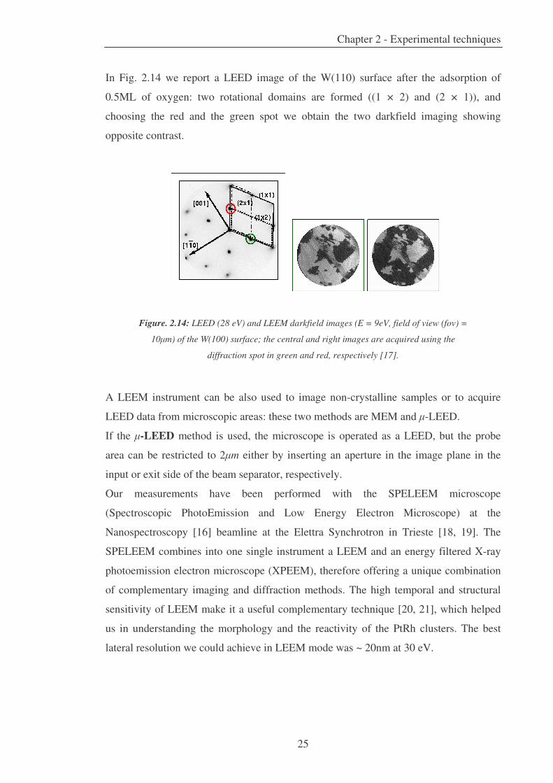
In Fig. 2.14 we report a LEED image of the W(110) surface after the adsorption of
0.5ML of oxygen: two rotational domains are formed ((1 × 2) and (2 × 1)), and
choosing the red and the green spot we obtain the two darkfield imaging showing
opposite contrast.
Figure. 2.14: LEED (28 eV) and LEEM darkfield images (E = 9eV, field of view (fov) =
10�m) of the W(100) surface; the central and right images are acquired using the
diffraction spot in green and red, respectively [17].
A LEEM instrument can be also used to image non-crystalline samples or to acquire
LEED data from microscopic areas: these two methods are MEM and �-LEED.
If the �-LEED method is used, the microscope is operated as a LEED, but the probe
area can be restricted to 2�m either by inserting an aperture in the image plane in the
input or exit side of the beam separator, respectively.
Our measurements have been performed with the SPELEEM microscope
(Spectroscopic PhotoEmission and Low Energy Electron Microscope) at the
Nanospectroscopy [16] beamline at the Elettra Synchrotron in Trieste [18, 19]. The
SPELEEM combines into one single instrument a LEEM and an energy filtered X-ray
photoemission electron microscope (XPEEM), therefore offering a unique combination
of complementary imaging and diffraction methods. The high temporal and structural
sensitivity of LEEM make it a useful complementary technique [20, 21], which helped
us in understanding the morphology and the reactivity of the PtRh clusters. The best
lateral resolution we could achieve in LEEM mode was ~ 20nm at 30 eV.
Chapter 2 - Experimental techniques
26
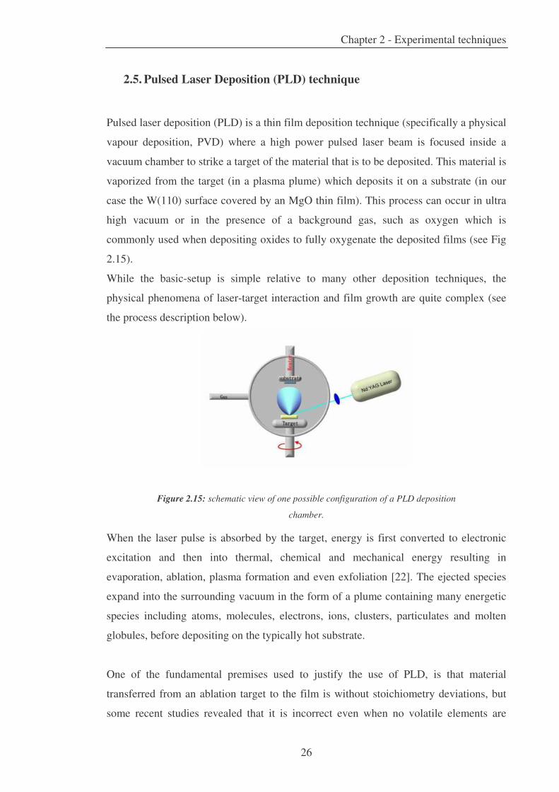
2.5. Pulsed Laser Deposition (PLD) technique
Pulsed laser deposition (PLD) is a thin film deposition technique (specifically a physical
vapour deposition, PVD) where a high power pulsed laser beam is focused inside a
vacuum chamber to strike a target of the material that is to be deposited. This material is
vaporized from the target (in a plasma plume) which deposits it on a substrate (in our
case the W(110) surface covered by an MgO thin film). This process can occur in ultra
high vacuum or in the presence of a background gas, such as oxygen which is
commonly used when depositing oxides to fully oxygenate the deposited films (see Fig
2.15).
While the basic-setup is simple relative to many other deposition techniques, the
physical phenomena of laser-target interaction and film growth are quite complex (see
the process description below).
Figure 2.15: schematic view of one possible configuration of a PLD deposition
chamber.
When the laser pulse is absorbed by the target, energy is first converted to electronic
excitation and then into thermal, chemical and mechanical energy resulting in
evaporation, ablation, plasma formation and even exfoliation [22]. The ejected species
expand into the surrounding vacuum in the form of a plume containing many energetic
species including atoms, molecules, electrons, ions, clusters, particulates and molten
globules, before depositing on the typically hot substrate.
One of the fundamental premises used to justify the use of PLD, is that material
transferred from an ablation target to the film is without stoichiometry deviations, but
some recent studies revealed that it is incorrect even when no volatile elements are

Chapter 2 - Experimental techniques
27
involved [23]. The detailed mechanisms of PLD are very complex including the
ablation process of the target material by the laser irradiation, the development of a
plasma plume with high energetic ions, electrons as well as neutrals and the crystalline
growth of the film itself on the heated substrate. The process of PLD can generally be
divided into four stages:
- Laser ablation of the target material and creation of a plasma
- Dynamic of the plasma
- Deposition of the ablation material on the substrate
- Nucleation and growth of the film on the substrate surface
Each of these steps is crucial for the degree of crystallinity, uniformity and
stoichiometry of the resulting film.
Laser ablation of the target material and creation of a plasma
The ablation of the target material upon laser irradiation and the creation of plasma are
very complex processes. The removal of atoms from the bulk material is done by
vaporization of the bulk at the surface region in a state of non-equilibrium and is caused
by a Coulomb explosion. In this the incident laser pulse penetrates into the surface of
the material within the penetration depth. This dimension is dependent on the laser
wavelength and the index of refraction of the target material at the applied laser
wavelength and is typically in the region of 10 nm for most materials. The strong
electrical field generated by the laser light is sufficiently strong to remove the electrons
from the bulk material of the penetrated volume. This process occurs within 10 ps of a
ns laser pulse and is caused by non-linear processes such as multiphoton ionization
which are enhanced by microscopic cracks at the surface, voids, and nodules, which
increase the electric field. The free electrons oscillate within the electromagnetic field of
the laser light and can collide with the atoms of the bulk material thus transferring some
of their energy to the lattice of the target material with in the surface region. The surface
of the target is then heated up and the material is vaporized.
Dynamic of the plasma
In the second stage, the material expands in a plasma parallel to the normal vector of the
target surface towards the substrate due to Coulomb repulsion and recoils from the
target surface. The spatial distribution of the plume is dependent on the background

Chapter 2 - Experimental techniques
28
pressure inside the PLD chamber. The density of the plume can be described by a law
with a shape similar to a Gaussian curve. The dependency of the plume shape on the
pressure can be described in three stages: (i) the vacuum stage, where the plume is very
narrow and forward directed; almost no scattering occurs with the background gases.
(ii) The intermediate region, where a splitting of the high energetic ions from the less
energetic species can be observed. (iii) High pressure region where we find a more
diffusion-like expansion of the ablated material. Naturally this scattering is also
dependent on the mass of the background gas and can influence the stoichiometry of the
deposited film.
The most important consequence of increasing the background pressure is the slowing
down of the high energetic species in the expanding plasma plume. It has been shown
that particles with kinetic energies around 50 eV can resputter the film already
deposited on the substrate. This results in a lower deposition rate and can furthermore
result in a change in the stoichiometry of the film.
Deposition of the ablation material on the substrate
The third stage is important to determine the quality of the deposited films. The high
energetic species ablated from the target are bombarding the substrate surface and may
cause damage to the surface by sputtering off atoms from the surface but also by
causing defect formation in the deposited film. The sputtered species from the substrate
and the particles emitted from the target form a collision region, which serves as a
source for condensation of particles. When the condensation rate is high enough, a
thermal equilibrium can be reached and the film grows on the substrate surface at the
expense of the direct flow of ablation particles and the thermal equilibrium obtained.
Nucleation and growth of the film on the substrate surface
The nucleation process and growth kinetics of the film depend on several growth
parameters including the laser parameters, like the laser fluence [Joule/cm2] that can
affect the stoichiometry of the film [23], the surface temperature [24], the condition of
the substrate surface [25] and the background pressure [26]
Chapter 2 - Experimental techniques
29
2.6. Other Techniques of Surface Science used: AES , SEM and EDX
The aim of this section is to give a brief overview of the other techniques of
investigation used mainly in the preparation of the W(110) surface.
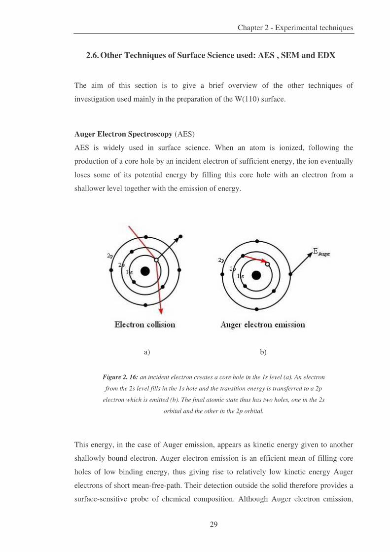
Auger Electron Spectroscopy (AES)
AES is widely used in surface science. When an atom is ionized, following the
production of a core hole by an incident electron of sufficient energy, the ion eventually
loses some of its potential energy by filling this core hole with an electron from a
shallower level together with the emission of energy.
a) b)
Figure 2. 16: an incident electron creates a core hole in the 1s level (a). An electron
from the 2s level fills in the 1s hole and the transition energy is transferred to a 2p
electron which is emitted (b). The final atomic state thus has two holes, one in the 2s
orbital and the other in the 2p orbital.
This energy, in the case of Auger emission, appears as kinetic energy given to another
shallowly bound electron. Auger electron emission is an efficient mean of filling core
holes of low binding energy, thus giving rise to relatively low kinetic energy Auger
electrons of short mean-free-path. Their detection outside the solid therefore provides a
surface-sensitive probe of chemical composition. Although Auger electron emission,

Chapter 2 - Experimental techniques
30
being a three-level process, is intrinsically more complex than photoemission, its
usefulness lies in the fact that it can be generated by incident electron beams and that
the production, focusing and deflection or scanning of electron beams is a well-
developed technology [27]. For the present case the Auger spectrum was simply used as
a fingerprint of the chemical composition at the surface.
Scanning Electron Microscopy (SEM)
SEM uses a focused electron beam to raster scan a sample; as the beam strikes each
point on the specimen, various responses are produced due to electron-sample
interactions. Several of these responses can be collected by suitable detectors to form
the image. The most frequently used response in a conventional SEM is the detection of
the secondary electrons generated by the primary electron beam. Secondary electrons
are ejected from the sample as a result of ionization processes. The yield of these
electrons depend on various factors such as the accelerating voltage applied to the
primary beam electrons and the atomic number of the elements included in the sample.
As the yield is very much dependent on the angle of incidence of the primary beam,
topographical contrast is high.
SEMs can provide extremely high spatial resolution (less then 5 nm) and when the
sample is sufficiently conductive it can often be imaged without special sample
preparations.
During the present experiments a SEM Zeiss (SEM equipped with a Field Emission
Gun) has been used to characterize the cluster’s morphology and structure and to check
for the presence of small clusters with dimensions smaller than the SPEM resolution.
Energy-dispersive X-ray spectroscopy (EDX)
Energy dispersive X-ray spectroscopy (EDX) is an analytical technique used for the
elemental analysis or chemical characterization of a sample, often used in conjunction
with a SEM.
The EDX technique detects x-rays emitted from the sample during bombardment by an
electron beam to characterize the elemental composition of the analyzed volume.
Its characterization capabilities are due in large part to the fundamental principle that
each element has a unique atomic structure allowing X-rays that are characteristic of an
element's atomic structure to be identified uniquely from each other. When the sample
Chapter 2 - Experimental techniques
31
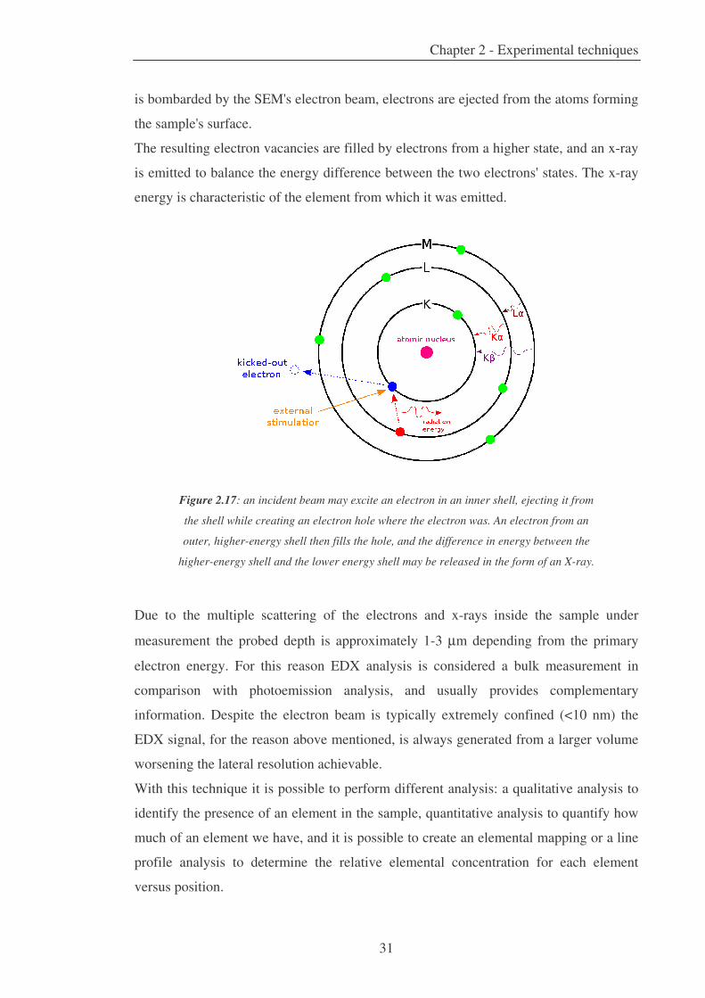
is bombarded by the SEM's electron beam, electrons are ejected from the atoms forming
the sample's surface.
The resulting electron vacancies are filled by electrons from a higher state, and an x-ray
is emitted to balance the energy difference between the two electrons' states. The x-ray
energy is characteristic of the element from which it was emitted.
Figure 2.17: an incident beam may excite an electron in an inner shell, ejecting it from
the shell while creating an electron hole where the electron was. An electron from an
outer, higher-energy shell then fills the hole, and the difference in energy between the
higher-energy shell and the lower energy shell may be released in the form of an X-ray.
Due to the multiple scattering of the electrons and x-rays inside the sample under
measurement the probed depth is approximately 1-3 µm depending from the primary
electron energy. For this reason EDX analysis is considered a bulk measurement in
comparison with photoemission analysis, and usually provides complementary
information. Despite the electron beam is typically extremely confined (<10 nm) the
EDX signal, for the reason above mentioned, is always generated from a larger volume
worsening the lateral resolution achievable.
With this technique it is possible to perform different analysis: a qualitative analysis to
identify the presence of an element in the sample, quantitative analysis to quantify how
much of an element we have, and it is possible to create an elemental mapping or a line
profile analysis to determine the relative elemental concentration for each element
versus position.
Chapter 2 - Experimental techniques
32
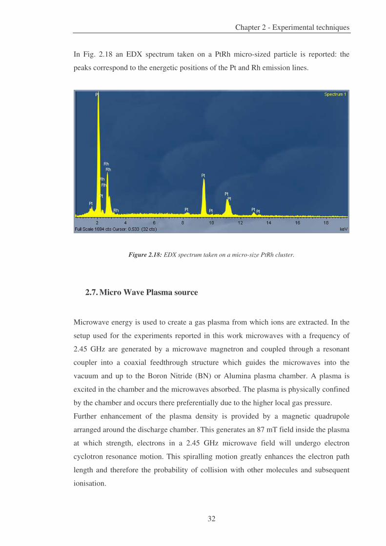
In Fig. 2.18 an EDX spectrum taken on a PtRh micro-sized particle is reported: the
peaks correspond to the energetic positions of the Pt and Rh emission lines.
Figure 2.18: EDX spectrum taken on a micro-size PtRh cluster.
2.7. Micro Wave Plasma source
Microwave energy is used to create a gas plasma from which ions are extracted. In the
setup used for the experiments reported in this work microwaves with a frequency of
2.45 GHz are generated by a microwave magnetron and coupled through a resonant
coupler into a coaxial feedthrough structure which guides the microwaves into the
vacuum and up to the Boron Nitride (BN) or Alumina plasma chamber. A plasma is
excited in the chamber and the microwaves absorbed. The plasma is physically confined
by the chamber and occurs there preferentially due to the higher local gas pressure.
Further enhancement of the plasma density is provided by a magnetic quadrupole
arranged around the discharge chamber. This generates an 87 mT field inside the plasma
at which strength, electrons in a 2.45 GHz microwave field will undergo electron
cyclotron resonance motion. This spiralling motion greatly enhances the electron path
length and therefore the probability of collision with other molecules and subsequent
ionisation.

Chapter 2 - Experimental techniques
33
Figure 2.18: the Tectra Gen2 Plasma Source mounted at the ESCAmicroscopy
beamline.
The open end of the plasma chamber is closed with a grid of holes. When operated as an
ion source, the grid is made from molybdenum or other materials. Positive voltage
applied to this grid accelerates ions from the plasma out into the chamber. An additional
grid is provided to assist with ion extraction and beam current control. It also helps
preventing electron back-streaming where an ion beam neutraliser is employed.
When the instrument is operated as an atom source or plasma source, the metal grids are
replaced by aperture plates (BN or Alumina) with a number of small holes.
The specially designed aperture plate inhibits ions from escaping from the plasma, yet
allows reactive neutrals to escape and form the dominant beam fraction. The emitted
particles are largely thermalised through multiple collisions on passing through the
aperture. These neutrals have proven to be very effective in low damage surface
treatments such as nitridation and oxidation. [28, 29]
The further addition of an ion-trap option can completely remove the residual ion
content from the beam where this may be of concern.
A hybrid mode is also available in which metal and dielectric grids are combined to
produce a source which functions principally as an atom source but where a small ion
current can also be added to the beam.

Chapter 2 - Experimental techniques
34
References
1. Robinson, H. and Rawlinson, W. J. Philosophical Magazine 1914, 28, 277.
2 Robinson, H. Philosophical Magazine 1925, 50, 241.
3 Siegbahn, K. et al. ”ESCA: atomic, molecular and solid state structure studied by
means of electron spectroscopy„ 1967, Almquist and Wilsells, Uppsala.
4 Himpsel, F. J. Surf. Sci. 1994, 299, 525.
5. Pehlke, E.; Scheffler, M. Phys. Rev. Lett. 1993, 71, 2338.
6 Osten, H. J.; Methfessel, M.; Lippert, G.; Rucker, H. Phys. Rev. B 1995, 52, 12179.
7 Briggs, J.; Seah, M.P. “Practical Surface Analysis” Wiley, 1990.
8 “Handbook on Synchrotron Radiation” edited by Ernst-Ekhard Kock – North Holland
(1983).
9 “Synchrotron Radiation Research” edited by H. Winick – S. Doniach – Plenum Press
(1980).
10. Oura, K.; Lifshifts, V.G.;. Saranin, A.A.; Zotov, A.V.; Katayama, M. Surface
Science 2003 Springer-Verlag, Berlin Heidelberg New York. pp.1–45.
11 Christmann, K. Introduction to Surfaces Physical Chemistry, 1991.
12 Ertl, G.; Kuppers, J. Low Energy Electrons and Surface Chemistry, Verlag Chemie,
1985.
13 Bauer, E. Ultramicroscopy 1985, 17, 51.
14 Bauer, E. Surface Review and Letters 1998, 5, 1275.
15 Bauer, E. Rep. Prog. Phys. 1994, 54, 895-938.
16 URL http://www.elettra.trieste.it/nanospectroscopy.
17 Mentes, T. O.; Stojic, N.; Binggeli, N.; Locatelli, A.; Aballe, L.; Kiskinova, M.;
Bauer, E. Phys. Rev. B 2008, 77, 155414.
18 Schmidt, T.; Heun, S.; Slezak, J.; Diaz, J.; Prince, J.C.; Lilienkamp, G.; Bauer, E.
Surface Review and Letters 1998, 5, 1287.
19 Günther, S.; Kaulich, B.; Gregoratti, L.; Kiskinova, M. Progr. Surf. Sc. 2002, 70,
187.
20 Locatelli, A.; Sbraccia, C.; Heun, S.; Baroni, S.; Kiskinova, M. Journal of the
American Chemical Society 2005, 127, 2351.
21 Locatelli, A.; Mentes, T.O.; Aballe, L.; Mikhailov, A.; Kiskinova, M. The Journal of
Physical Chemistry B Letters 2006, 110, 19108.

Chapter 2 - Experimental techniques
35
22 Chrisey, D.B.; Hubler, G.K. Pulsed Laser Deposition of Thin Films, edited by, John
Wiley & Sons, 1994
23 Ohnishi, T. et al. Journal of Applied Physics 2008, 103, 103703
24 Ferguson, J.D. et al. Phys. Rev. Lett. 2009, 103, 256103.
25 Koster, G. et al. Applied Physics Letters 1998, 73, 2920.
26 Ohtomo, A.; Hwang, H.Y. Journal of Applied Physics 2007, 102.
27 Woodruff, D.P.; Delchar, T.A. “Modern techniques of surface science”, Cambridge,
1994.
28 Schmidt, A.A.; Offermann, J.; Anton, R. Thin Solid Films 1996, 281-282, 105-107.
29 Anton, R.; Wiegner, T.; Naumann, W.; Liebmann, M.; Klein, C.; Bradley, C.
Rev.Sci.Instr. 2000.

Chapter 3 - Sample preparation and characterization
36
Chapter 3
Sample preparation and
characterization
As previously stated in the introduction, one of the fastest-developing fields in surface
science is research on nanoclusters of semiconducting and metallic materials. The latter
have been studied in many different ways: as free clusters, as embedded in a host matrix
or as deposited onto a support. The last type is certainly the most relevant for real-world
heterogeneous catalysis applications.
A typical supported metal catalyst is usually deposited on a thermally stable and
surface-rich oxide support material, such as alumina (Al2O3), magnesium oxide (MgO)
or silica (SiO2). On these oxides, well-dispersed metal particles typically in the size
range of a few nanometers are prepared via, for example, impregnation of a precursor
followed by suitable chemical and thermal treatment (though other methods exist). The
role of the support is well described in the literature [1] and is based on several effects.
The first is the modification of nanoclusters’ electronic properties induced by the
particle-support interactions. The second is the diffusion of the reactants through the
surface.
One of the best choices for modelling real oxide-supported catalysts using the surface
science approach is the deposition of nanoclusters on an ultra-thin oxide film, which in
turn is supported by a conductive material.
The choice of the supported thin films is a compromise between two needs. First of all,
we wish to model a real catalyst composed by metal particles supported by a metal

Chapter 3 - Sample preparation and characterization
37
oxide. However, performing measurements on metal nanoclusters on an oxide support is
non-trivial, because almost all metal oxides are nonconductive. Most surface science
experimental techniques (XPS, STM and in general all electron microscopies and
spectroscopies) cannot be easily employed if the support is an electrical insulator: the
sample undergoes charging, which strongly influences the measurements. Metal oxide
thin films represent one solution to this problem. It has been shown that even films with
a thickness of just a few angstroms can exhibit physical properties characteristic of the
bulk material. [2, 3] Using an oxide layer of a thickness between 10 and 20 Å,
supported by a metal substrate, we obtain two critical desirable characteristics:
- support conductivity: the metal substrate is naturally conductive, and the oxide
thin film becomes practically conductive because the reduced thickness opens a
significant tunneling channel.
- real oxide behaviour: the oxide layer is thick enough to isolate the surface from
metallic substrate influence so the nanocluster support is an almost real oxide.
Of course the creation of this oxide/metal support depends critically on the choice of the
metal substrate, which must be done in a way so as to match the two lattice constants
and to create understandable interactions between the two materials.
Many investigations have been conducted on MgO supported nanoclusters, focusing on
both electronic and structural properties, as well as chemical reactivity as in the case of
Pd [4] and Au [5] nanoclusters.
For the reasons explained above, PtRh clusters were deposited on an ultrathin 2-3 nm
MgO film grown on the (110) surface of a tungsten single crystal.
W(110) sample was cleaned in UHV by Ar ion sputtering followed by annealing at
990°C in a pressure of 2x10⁻⁸ mbar for one day, followed by a number of fast annealing,
in UHV and in presence of oxygen (10-6 mbar), till a temperature of 1775° C for
removing completely the presence of carbon and oxygen. This check was performed by
means of AES measurements. A final LEED measure was made for inspecting the
surface reconstruction.
�

Chapter 3 - Sample preparation and characterization
38
�
�
Figure 3.1: W(110) single crystal sample mounted on the sample holder
The MgO films were prepared by growing first a thin epitaxial Mg layer on the clean
W(110) sample at RT in UHV for 5 min (the deposition rate of Mg was ~0.5 ML/min),
followed by a deposition of Mg in oxygen ambient (3×10⁻⁶ mbar) for other 15 min.
�
Figure 3. 2: sketch of the MgO deposition. MgO films were prepared by growing first a
thin epitaxial Mg layer on the clean W(110) sample at RT in UHV for 5 min (the
deposition rate of Mg was ~0.5 ML/min), followed by a deposition of Mg in oxygen
ambient (3×10⁻⁶ mbar) for other 15 min. After that PtRh clusters were deposited by
PLD.
The catalyst layer was prepared via Pulsed Laser Deposition by ablating a Pt50Rh50
target with a Nd:YAG laser operated at 10 Hz repetition rate and 10 ns pulse width. The
ablated platinum-rhodium target was placed in the focal spot of the focusing optics
illuminated with both 532 and 1064 nm harmonics of the laser. The calibration
MgO
PtRh clusters
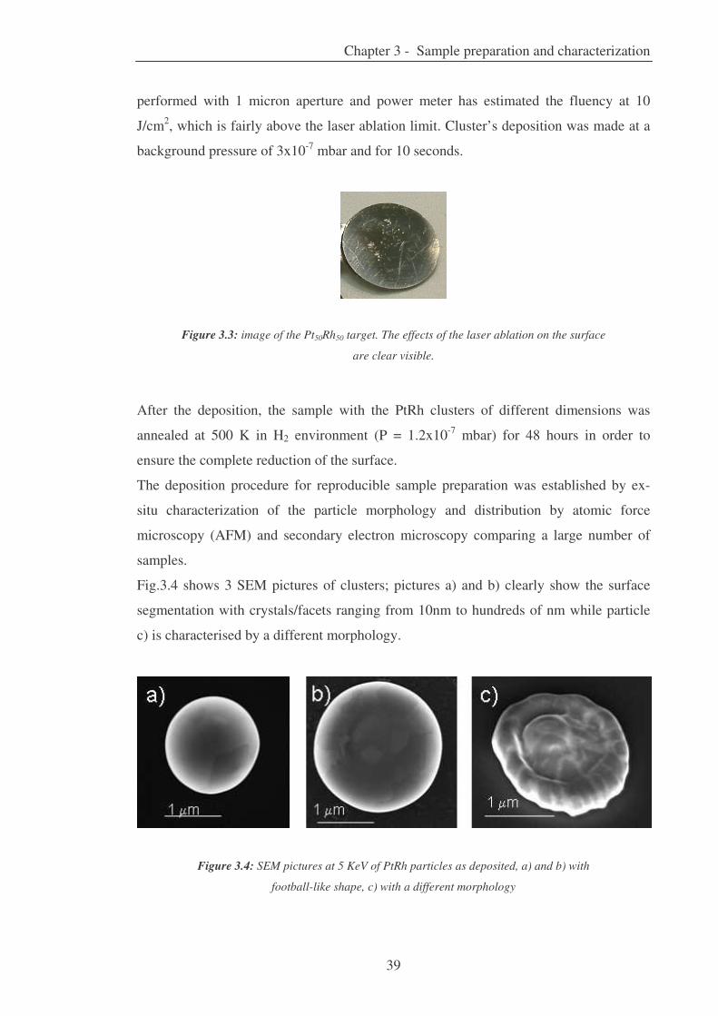
Chapter 3 - Sample preparation and characterization
39
performed with 1 micron aperture and power meter has estimated the fluency at 10
J/cm2, which is fairly above the laser ablation limit. Cluster’s deposition was made at a
background pressure of 3x10⁻⁷ mbar and for 10 seconds.
�
�
Figure 3.3: image of the Pt50Rh50 target. The effects of the laser ablation on the surface
are clear visible.
After the deposition, the sample with the PtRh clusters of different dimensions was
annealed at 500 K in H2 environment (P = 1.2x10⁻⁷ mbar) for 48 hours in order to
ensure the complete reduction of the surface.
The deposition procedure for reproducible sample preparation was established by ex-
situ characterization of the particle morphology and distribution by atomic force
microscopy (AFM) and secondary electron microscopy comparing a large number of
samples.
Fig.3.4 shows 3 SEM pictures of clusters; pictures a) and b) clearly show the surface
segmentation with crystals/facets ranging from 10nm to hundreds of nm while particle
c) is characterised by a different morphology.
Figure 3.4: SEM pictures at 5 KeV of PtRh particles as deposited, a) and b) with
football-like shape, c) with a different morphology

Chapter 3 - Sample preparation and characterization
40
The chosen deposition parameters resulted in a low particle density, approximately 1
particle/104 µm2 for particles of size between 50-1000 nm, while the density of the
smaller ones (< 50 nm) was below the critical value for producing a continuous film.
Figure 3.5: low magnification SEM image of the surface of the sample after a PLD
deposition.
As shown in Fig.3.5, this particle distribution allowed us to investigate the behaviour of
isolated single particles excluding any proximity interaction effect.
The AFM and SEM characterization of samples showed that approximately 10% of the
MgO support surface is covered with nano-particles of average size around 5 nm (see
Fig. 3.6), whereas the particles larger than 100 nm, which were detectable also with
SPEM, are a minority.
Figure 3.6: high magnification SEM image of the surface of the sample around the big
particles. Small clusters with an average size of 5 nm cover approximately 10% of the
surface
10 µm
20 nm

Chapter 3 - Sample preparation and characterization
41
According to the statistical analysis of the shapes the football-like (Fig. 3.7a) and
volcano-like (Fig. 3.7b) ‘large’ particles are almost equally distributed. The intensity
variations of the high-resolution SEM images in Fig. 3.7 indicate that both types of
‘large’ particles have a similar complex morphology with well-defined uniform regions
composing a puzzle on the particle surface.
a) b)
Figure 3.7: SEM images of islands with accentuated (a) a football-like (b) donut-like
shape
Since along with topography the local surface structure can also contribute to the SEM
contrast, this suggests coexistence of regions with a different plane orientation, which
was confirmed by the LEEM measurements, described in the next chapter. Apparently,
the surface morphology of both ‘large’ particles accounts for the very similar chemical
and structural evolution we observed under oxidation conditions.
Due to the deposition process of the particles also the surface of the bigger ones is
covered by the smaller clusters. We tried to find the presence of that nano-sized
particles on the surface of the larger ones acquiring high resolution SEM and AFM
images. In both cases it was not possible to reveal the presence of such small clusters.
We are confident that the reason must be attributed to the pronounced topography which
characterises the particles which artificially modify the contrast in the acquired images
(SEM) or makes almost impossible to perform a continuous and linear scan (AFM); the
geometry of the tip of the AFM is indeed not compatible with the spherical shape of the
200 nm 200 nm

Chapter 3 - Sample preparation and characterization
42
clusters as we can see in Fig.3.8. In the flat region, in fact, as shown above the small
clusters are well visible (see Fig. 3.6).
Figure 3.8: AFM 3D image taken on a big particle in non-contact mode.
Fig. 3.9 shows an AFM phase image taken on a big cluster. This kind of images gives
information mainly on the main morphology of the particles. Even by using the non-
contact image acquisition mode it was very difficult to distinguish in the images the
presence of the well ordered facets as clearly viewed in the SEM pictures. In Fig. 3.9
one of these images has been shown. Despite the main borders of the particle are seen
and changes in the contrast occur in the central part of the cluster it is almost impossible
to relate such contrasts to the oriented facets.
Figure 3.9: AFM phase image of a big cluster in non-contact mode
1 µm
Chapter 3 - Sample preparation and characterization
43
References
1 Libuda, L.; Freund, H-J. Surf. Sci. Rep. 2005, 57, 157.
2 Freund, H.-J. Phys Status Solid B 1995, 192, 407.
3 Schintke, S.; Messerli, S.; Pivetta, M.; Patthey, F.; Libioulle, L.; Stengel, M.; De Vita,
A.; Schneider, W.-D. Phys Rev Lett 2001, 87, 276801.
4. Nolte, P.; Stierle, A.; Balmes, O.; Srot, V.; van Aken, P.A.; Jeurgens, L.P.H.; Dosch,
H Cat. Today 2009, 145, 243.
5. Yulikov, M.; Sterrer, M.; Heyde, M.; Rust, H.-P.; Risse, T.; Freund, H.-J.; Pacchioni,
G. ; Scagnelli, A Phys. Rev. Lett. 2006, 96, 146804.

Chapter 4 - Oxidation states of single particles monitored by SPEM
44
Chapter 4
Oxidation states of single particles
monitored by SPEM
4.1. Working conditions
The chemical characterization of the PtRh particles deposited on the MgO film was
performed with the scanning photoemission microscope (SPEM) described in chapter 2.
Under the experimental conditions the lateral resolution was better than 100 nm in the
imaging mode and ~160 nm in microspot spectroscopy. The measurements were carried
out using 640 eV photon energy and overall spectral energy resolution of 220 meV in
microspot spectroscopy and ~320 meV (Rh) and 490 meV (Pt) in spectroimaging mode.
For the deconvolution of the Pt and Rh core-level spectra the well-developed procedure
with Doniach-Sunjic functions convoluted with Gaussians was used, accounting for the
experimental resolution and broadening due to different factors. [1]
For the oxidation of the samples we used an atomic oxygen plasma source, as the one
described in chapter 2, which allowed us to reach advanced oxidation states keeping the
background O2 pressure below 10-5 mbar. The upper limit of the atomic oxygen flux in
the vicinity of the sample surface was estimated to be ~ 1013 atoms/s × cm2. The overall
oxygen dose was controlled by the exposure time.
4.2. Results
In both Rh 3d5/2 and Pt 4f7/2 maps, which provide identical shape-size-morphology
information, the ‘large’ PtRh particles, covering a very small fraction of the support,

Chapter 4 - Oxidation states of single particles monitored by SPEM
45
appear as distinct bright features. Fig. 4.1 is a large scanning SPEM map taken on the Pt
energy where it is possible to identify bright islands that correspond to a big PtRh
clusters. Once one of them is found it is possible to focus on it and perform more
detailed image and acquire spectra.
Figure 4.1: SPEM image taken at the Pt energy. The brighter island is a PtRh micro sized cluster.
The areas surrounding the ‘large’ particles are covered with non-resolvable by SPEM
nano-particles and appear flat in the Rh and Pt maps with weak variations in the contrast
level reflecting a non-uniform cluster density. According to a simple calculation the
very low Rh 3d5/2 and Pt 4f7/2 intensity in these regions suggests that the nano-particles
cover less than 10% of the MgO surface.
Figure 4.2: Pt 4f map of a single micro-particle. The white circle highlights the real size including the shadowed region at the left. Positions labeled A and B indicate the points
where the spectra reported in the next figures were measured. This particle is characterized by a complex morphology, resulting in sensible contrast variations in the
SPEM images.
0.5 µm
60 µm
0.5 µm

Chapter 4 - Oxidation states of single particles monitored by SPEM
46
As will be shown later there is a direct correlation of the morphology variations to the
reactivity of the different particle regions. It should be noted that the brightest and
darkest regions on the right and left hand side of the particle are artefacts due to height-
related enhancement and shadowing of the emitted photoelectrons, respectively. [2]
The Rh3d5/2 spectra of the particle in Fig. 4.2, taken before and after two oxidation
cycles are summarised in Fig. 4.3 and compared to the spectra acquired on the
surrounding “flat” regions covered with nano-particles.
The Rh 3d5/2 spectra measured at different regions of the reduced particle have identical
shapes and intensity spread corresponding to the contrast variation in the Fig. 4.2. The
best deconvolution of these spectra requires two components at binding energy (BE)
307.2 eV and 306.8 eV, in fair agreement with 307.1 eV and 306.6 eV values, reported
for PtRh(100), as bulk and surface components, respectively. [3] However, compared to
the Rh 3d5/2 spectra of a well-ordered PtRh(100) alloy the ones of the particles are
broader, and the surface component is very weak, indicating that the coexisting
differently oriented planes have a poor long range order or very small dimensions. As a
reference for the energy position of metallic Rh, which remains unchanged in the PtRh
alloy [3], we show in the bottom of panel (a) the Rh 3d5/2 spectrum of a Rh(100) single
crystal, measured with our experimental setup. The spectrum from the ‘flat’ region with
a maximum at 307.7 eV represents the averaged spectrum of nano-particles of variable
sizes. Accordingly, it is very broad and without statistical analysis of the particle size
distribution any tentative deconvolution is speculative. However, the higher binding
energy of the peak maximum suggests dominance of clusters smaller than 10 nm, when
the size starts to exert sensible initial and final state effects on the energy of emitted
core level electrons. [4]
The evolution of the Rh3d5/2 spectra taken from different spots on the ‘large’ particles
upon oxidation showed sensible site dependence. The lateral heterogeneity of the
oxidation states developed within the same micro-particle is represented better by the
two spectra recorded in the selected spots (A and B) indicated in Fig. 4.2. We would
like to note that these spectra represent only two regions of the complex oxidation
anisotropy of the particle, which is revealed by the chemical maps described below.

Chapter 4 - Oxidation states of single particles monitored by SPEM
47
311 310 309 308 307 306
Binding Energy (eV)
A
B
B
A
A/B
Rh(100)
Initialstate
195' Oxidation
715' Oxidation
Rh3d5/2
'flat'
a)
b)
c)
x10
Rhmet
RhOx<1.5
Rh2O3RhO2
'flat'x10
'flat'x10
Figure 4.3: Rh 3d5/2 spectra acquired in points A and B as indicated in Fig.4.2 and in a ‘flat’ region covered with nano-particles: (a) before exposing to atomic oxygen; (b) after
195’ exposure (dose of ~1017 at.cm2); (c) after 715’ exposure (dose of ~4.1017 at.cm2). The Rh 3d5/2 spectrum of a clean Rh(100) single crystal is shown in the bottom as an
energy reference. The energy positions of the main components considered in the deconvolution of the spectra are indicated with dashed lines.

Chapter 4 - Oxidation states of single particles monitored by SPEM
48
After the first oxygen dose of 195’ (Fig.4.3 -panel (b)) the deconvolution of Rh3d5/2
spectra requires three components: one metallic and two peaked at higher BE, 307.6-
307.7 eV and 308.1-308.2 eV, respectively. In accordance with previous studies [5], the
first peak can be assigned to surface oxide, RhOx, while the highest BE one indicates
the growth of a Rh2O3 phase, becoming more pronounced with advancement of the
oxidation process. By comparing the spectra taken in points A and B, it is obvious that
the region B is in a more advanced oxidation state. The different local activity of the
different particle regions towards oxidation becomes more evident at higher oxygen
exposure (715’) when the metallic component is completely suppressed and a new
component at 309.0 eV, assigned to a RhO2 state, emerges in the spectrum from region
B, while in region A the Rh2O3 component becomes dominant.
Accordingly, the spectra from the ‘flat’ region become broader and shift towards higher
BE. The actual oxidation state of the nano-particles cannot be well defined, since the
size-induced shift is not necessarily the same for metallic and oxidized states. However,
after the second dose the energy window of the spectra indicates that the nano-particles
are fully oxidized and higher oxidation states dominate.
The corresponding evolution of the Pt 4f7/2 spectra upon oxidation is shown in Fig. 4.4
Here, as a reference for the Pt metallic component we measured the Pt(111) single
crystal surface, where the surface component is poorly resolved due to limited spectral
resolution. As can be expected, the Pt 4f7/2 spectrum of the particle in the initial state
requires a single bulk component at 71.0 eV. Similar to the Rh 3d5/2 spectra, the Pt 4f7/2
spectra from the ‘flat’ area are also very broad and shifted to higher BE with a
maximum at 71.6 eV. Compared to the Rh 3d5/2 spectra the Pt 4f7/2 ones undergo less
dramatic changes upon oxidation, in accordance with the lower affinity of Pt to oxygen.
The metallic component remains dominant even after the highest oxygen dose which
indicates that only the Pt top layers are oxidised. After the first oxygen dose, the
oxidation-related new components at 71.75 eV and 72.05 eV, respectively, are more
pronounced in the B region spectra. They can be tentatively assigned to the PtOx<1
transient surface oxide and PtO phases, in accordance with the previous reports [6, 7].
The Pt spectra undergo more dramatic changes after the second oxygen dose, when a
third component at 73.0 eV grows as well.
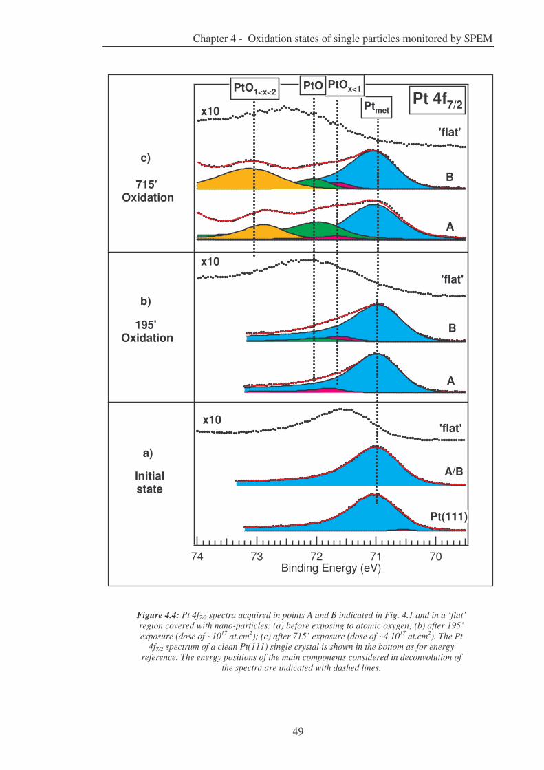
Chapter 4 - Oxidation states of single particles monitored by SPEM
49
74 73 72 71 70Binding Energy (eV)
A
A
B
Pt(111)
A/B
a)
b)
c)
Initialstate
195' Oxidation
715' Oxidation
Pt 4f7/2
'flat'
B
x10 Ptmet
PtOx<1PtOPtO1<x<2
'flat'x10
'flat'
x10
Figure 4.4: Pt 4f7/2 spectra acquired in points A and B indicated in Fig. 4.1 and in a ‘flat’ region covered with nano-particles: (a) before exposing to atomic oxygen; (b) after 195’ exposure (dose of ~1017 at.cm2); (c) after 715’ exposure (dose of ~4.1017 at.cm2). The Pt
4f7/2 spectrum of a clean Pt(111) single crystal is shown in the bottom as for energy reference. The energy positions of the main components considered in deconvolution of
the spectra are indicated with dashed lines.

Chapter 4 - Oxidation states of single particles monitored by SPEM
50
Since this BE is lower than the one reported for the PtO2 phase � 73.5 eV,[6, 7] we
tentatively attribute this state to a transient PtO1<x<2 phase. The higher weight of the
73.0 eV component in the spectrum from the B region confirms the site-dependent
oxidation trend evidenced by the Rh 3d5/2 spectra in Fig. 4.3. The evolution of the Pt
4f7/2 spectra within the nano-particles regions are also in accord with that of the Rh 3d5/2
spectra, indicating stronger Pt oxidation.
The relative depth of Rh and Pt oxidation in the particles can be elucidated from the
attenuation of the metallic Rh and Pt components, using the classical photoelectron
escape depth relationship and considering that the maximum probing depth under our
experimental conditions is ~10 �. We estimated for the highest oxygen doses that at
least three atomic layers of Rh atoms are oxidized (~ 7-8 �), and in some regions (e.g.
B) the extinction of the bulk component means that the oxidation depth exceeds 10 �
(~four layers). The Pt atoms are much more resistant to oxidation and the oxide
formation is limited to the top two layers (3-4 �). This means that the active catalytic
state of the PtRh alloy catalyst under realistic oxidation-reduction conditions is
characterized by very different Rh and Pt oxidation states at the surface and in the
subsurface regions.
As explained in section 2.2.3 thanks to the multichannel electron detector it is possible
to acquire within a single image several chemical maps and to extract spectra from some
region inside the image.
The contrast of the Rh maps in Fig. 4.5 corresponds to the summed signal from all 48
channels covering the energy window of the Rh 3d5/2 electron emission. As noted above,
the absolute intensity is strongly affected by the topography artefacts, which can be
removed using proper normalization procedures [2].
Figure 4.5: Rh 3d5/2 48-channels image. The colored squares indicate the regions within the particle where spectra were extracted and showed in Fig. 4.6.

Chapter 4 - Oxidation states of single particles monitored by SPEM
51
Despite the intensity artefact the lineshape of the reconstructed spectra from different
regions marked in Fig. 4.5 shown in Fig. 4.6 clearly evidences the spatial heterogeneity
in the Rh oxidation state.
Figure 4.6: reconstructed Rh 3d5/2 spectra taken from the three different regions within the particle showed in Fig. 4.5. The differences in the local oxidation state are clearly
manifested by the reconstructed spectra.
The chemical maps, illustrating the spatial distribution of the different Rh oxidation
states within the particle, are obtained by selecting channels covering the energy
window of the corresponding components and dividing by the total 48-channel signal to
remove the topography related artefacts.
The maps (Fig. 4.7) clearly show the coexistence of regions of different reactivity: it is
possible to distinguish the weakly (top and right), moderate (middle) and strongly
oxidized (bottom) regions where metallic Rh-RhOx, Rh2O3 or RhO2 state dominates.
Note that the electron emission contributing to the metallic Rh signal comes from the
atoms below the oxygen-containing top layers. The noisy region on the left side is the
shadowed area, which impedes a reliable chemical analysis.

Chapter 4 - Oxidation states of single particles monitored by SPEM
52
Figure 4.7: Rh 3d5/2 normalized chemical images of the RhO2, Rh2O3, RhOx, and Rhmet states. These images are generated by selecting the channels corresponding to a specific
chemical state in the reconstructed spectra.
The spatial heterogeneity of the Pt oxidation states is illustrated in Fig. 4.8.
Figure 4.8: reconstructed Pt 4f7/2 spectra taken from the three different regions within the particle showed in Fig. 4.5. The differences in the local oxidation state are clearly
manifested by the reconstructed spectra.
Rh metallic RhOx
Rh2O3 RhO2

Chapter 4 - Oxidation states of single particles monitored by SPEM
53
Although measured with a lower energy resolution in order to cover the wider Pt 4f7/2
energy range, one can clearly distinguish the main components, manifesting the
differences in the oxidation state within the particle.
As for Rh the lateral distribution of each Pt phase is shown in Fig. 4.9. The right-hand
border of the island is dominated by metallic and PtOx<1 states, replaced by PtO and
PtOx>1 states, moving towards the central part. Comparison with the Rh chemical maps
shows some correlations, e.g. both Rh and Pt appear in the lowest oxidation state in the
top-right regions, which supposes that the local structure plays a dominant role. Only
for the very bright stripe on the right-side edge, facing the grazing acceptance angle
analyser, we cannot rule out that the enhanced emission from the Rh and Pt metallic
atoms is not partially due to the local geometry, i.e. increased probing depth as a result
of increased taking-off emission angle.
Figure 4.9: Pt 4f7/2 images of a PtRh micro-particle The normalized Pt 4f7/2 chemical images are generated choosing the channels corresponding to a specific chemical states
in the reconstructed spectra.
The relative weight of the oxidation states within the particle elucidated from the
chemical maps is reported in Fig. 4.10.
Pt metallic PtOx<1
PtO PtOx>1

Chapter 4 - Oxidation states of single particles monitored by SPEM
54
Figure 4.10: Normalized distribution of the oxide phases on the PtRh particle evaluated by analyzing the data in Fig. 4.7 and Fig. 4.9.
The metallic state corresponds to the sub-surface atoms and reflects only the thickness
of the oxygen-containing top layers, which is apparently higher in the case of Rh. For Pt
the lowest oxidation PtOx<1 state is dominant, whereas Rh undergoes stronger oxidation
and the Rh2O3 dominates. It is quite clear from this plot that the top layers of the
particles, which determine its reactive properties, contain coexisting Pt and Rh
oxidation phases, which complicates the assignment of the reactivity to a single
chemical state. One should consider that each phase presents at this complex chemically
heterogeneous surface should has its local structure, which may play an important role
for creation of active sites and/or accommodation of transition reaction states. We
would like to notify that since the formed oxide phases have different stoichiometries
and thicknesses, we cannot judge possible Pt-Rh ratio changes (Rh or Pt segregation)
induced by the oxidation. As evidenced by the evolution of the surface structure under
oxidation described in the next section the formed Pt and Rh oxide phases under our
experimental conditions do not show any long-range order.

Chapter 4 - Oxidation states of single particles monitored by SPEM
55
References
1 Doniach, S.; Sunjic, M. J. Phys. C 1970, 3, 285
2 Günther, S.; Kolmakov, A.; Kovac, J.; Kiskinova, M. Ultramicroscopy 1998, 75 (1),
35-51
3 Baraldi, A.; Giacomello, D.; Rumiz, L.; Moretuzzo, M.; Lizzit, S.; Buatier De
Mongeot, F.; Paolucci, G.; Kiskinova, M. J. Am. Chem. Soc. 2005, 127, 5671-5674.
4 Mason, M.G. Phys. Rev. B 1983, 27 (2), 748-762
5 Dudin, P.; Barinov, A.; Gregoratti, L.; Scaini, D.; He, Y.B.; Over, H.; Kiskinova, M.
J. Phys. Chem. C 2008, 112, 9040–9044.
6 Parkinson, C.R.; Walker, M.; McConville, C.F. Surf. Sci. 2003, 545, 19-33
7 Yi-Chan, C.; Yu-Ming, S.; Shih-Ying, Y.; Chang-Po, H.; Jon-Yiew, G.; Chwung-
Shan, K. Nucl. Instr. And Meth. in Phys. Res. B 2002, 237, 296-300.
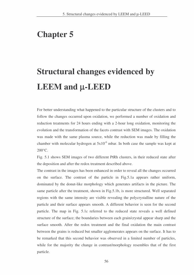
5. Structural changes evidenced by LEEM and µ-LEED
56
Chapter 5
Structural changes evidenced by
LEEM and µµµµ-LEED
For better understanding what happened to the particular structure of the clusters and to
follow the changes occurred upon oxidation, we performed a number of oxidation and
reduction treatments for 24 hours ending with a 2-hour long oxidation, monitoring the
evolution and the transformation of the facets contrast with SEM images. The oxidation
was made with the same plasma source, while the reduction was made by filling the
chamber with molecular hydrogen at 5x10⁻⁶ mbar. In both case the sample was kept at
200°C.
Fig. 5.1 shows SEM images of two different PtRh clusters, in their reduced state after
the deposition and after the redox treatment described above.
The contrast in the images has been enhanced in order to reveal all the changes occurred
on the surface. The contrast of the particle in Fig.5.1a appears rather uniform,
dominated by the donut-like morphology which generates artifacts in the picture. The
same particle after the treatment, shown in Fig.5.1b, is more structured. Well separated
regions with the same intensity are visible revealing the polycrystalline nature of the
particle and their surface appears smooth. A different behavior is seen for the second
particle. The map in Fig. 5.1c referred to the reduced state reveals a well defined
structure of the surface; the boundaries between each grain/crystal appear sharp and the
surface smooth. After the redox treatment and the final oxidation the main contrast
between the grains is reduced but smaller agglomerates appears on the surface. It has to
be remarked that this second behavior was observed in a limited number of particles,
while for the majority the change in contrast/morphology resembles that of the first
particle.
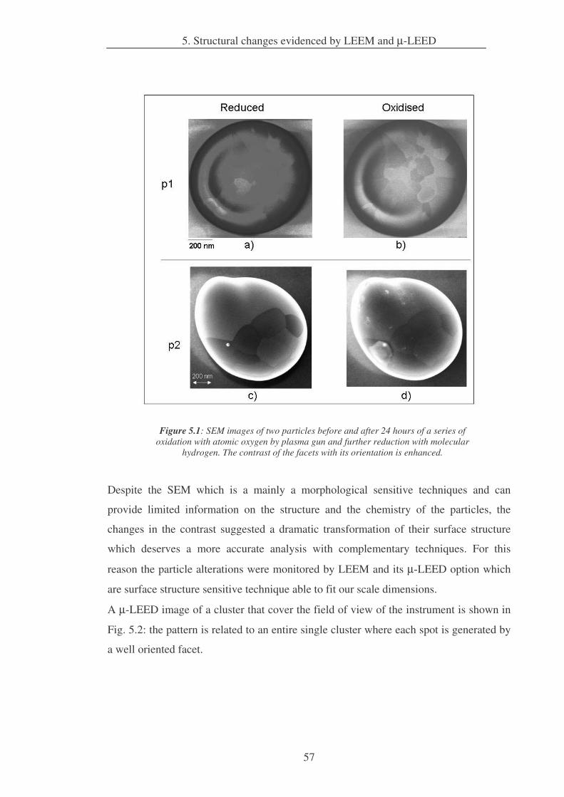
5. Structural changes evidenced by LEEM and µ-LEED
57
Figure 5.1: SEM images of two particles before and after 24 hours of a series of oxidation with atomic oxygen by plasma gun and further reduction with molecular
hydrogen. The contrast of the facets with its orientation is enhanced.
Despite the SEM which is a mainly a morphological sensitive techniques and can
provide limited information on the structure and the chemistry of the particles, the
changes in the contrast suggested a dramatic transformation of their surface structure
which deserves a more accurate analysis with complementary techniques. For this
reason the particle alterations were monitored by LEEM and its µ-LEED option which
are surface structure sensitive technique able to fit our scale dimensions.
A µ-LEED image of a cluster that cover the field of view of the instrument is shown in
Fig. 5.2: the pattern is related to an entire single cluster where each spot is generated by
a well oriented facet.

5. Structural changes evidenced by LEEM and µ-LEED
58
Figure 5.2: µ-LEED pattern related to an entire single particle where each spot is generated by a well oriented facet.
If the primary diffracted beam (or “00” beam) is selected to perform imaging (LEEM
Bright Field Imaging Mode) the resulting contrast in the maps is purely structural and
depends on the local changes in the diffraction properties of the different surface phases
present on the sample surface. The resulting image is shown in Fig. 5.3.
Figure 5.3: Bright Field Image of a cluster. All the facets that correspond to a single spot of the LEED in Fig. 5.2 have been made visible together in the same image.
If the secondary diffracted beam is selected (LEEM Dark Field Imaging Mode) than
only areas that contribute to the formation of the selected beam appear bright. In Fig.
5.4 few dark field images are shown; in each one a single facet that corresponds to a
specific spot energy in the µ−LEED pattern and that reveals the different structures of
several regions of the surface is visible.

5. Structural changes evidenced by LEEM and µ-LEED
59
Figure 5.4: Dark Field images taken at different spot energies revealing the different structures of several regions of the surface.
A 2-µm wide particle was selected for a LEEM and µ-LEED investigation of the effects
of the oxidation on the surface.
Prior to oxidation, the diffraction pattern (Fig. 5.5a) reveals the presence of several
well-defined facets with different orientations with respect to the surface normal. This
pattern reflects the existence of surface regions with a long range order, each producing
well defined spots. The dark-field LEEM images displayed in Fig. 5.5b clearly show
that each diffraction spot is identified with a nano-facet with sharp boundaries. Note
that, in order to illuminate more than a single facet, many dark field images are
superposed in Fig. 5.5b. Exposure to oxygen for 60’ leads to deterioration of the LEED
pattern and increasing the intensity of the diffuse background (see Fig. 5.5c).
Nevertheless, some of the original spots can still be recognized, which suggests that the
facets remain at least partially intact but with loss in the long range order. Indeed,
superposition of dark field images in Fig. 5.5d shows the same facet boundaries, but the
reduced contrast indicates different levels in structural deterioration between different
facets. This confirms that the oxidation process proceeds differently on each facet in
accordance with the observed spatial inhomogeneity in the oxidation states. Despite the
differences in the lateral resolution of LEEM and SPEM measurements comparing the

5. Structural changes evidenced by LEEM and µ-LEED
60
SPEM results in figures. 4.7 and 4.9 (previous chapter) with the LEEM ones in Fig. 5.5,
one can see that there is a good agreement between the SPEM chemical contrast and the
structural LEEM contrast.
Figure 5.5: (left) LEED patterns of a PtRh particle before and after a 60 and 715 min of oxygen exposures. Each diffraction spot is identified with a nano-facet in the
corresponding dark-field LEEM images (right), where many dark field images are superposed in order to illuminate more than a single facet.
This SPEM-LEEM correlation is a clear evidence that the oxidation rate is controlled by
the local structure of the different facets, which is in accordance with the reported
differences in the oxidation rate of differently oriented single crystal planes and the
5. Structural changes evidenced by LEEM and µ-LEED
61
‘promotion’ effect of structural irregularities [1]. More dramatic structural changes
resulting in the extinction of LEED spots occur upon stronger oxidation. The LEED
pattern from a heavily oxidized particle in Fig. 5.5e, shows only a strong diffuse
background without any detectable diffraction spots. The loss of ordered atomic
structure is confirmed by the corresponding LEEM image in Fig. 5.5f, which
corresponds to an uniform disordered surface. According to the photoemission spectra
in figures 4.6 and 4.8 this advanced oxidation state is characterised by rather thick O-
rich Rh oxide phases while Pt undergoes milder oxidation, but the lateral variation in
the oxidation state, i.e. the difference in the local reactivity is preserved. The fact that
we still distinguish by SPEM coexistence of more than one Rh and Pt oxidation state
within the regions appearing ‘homogeneous’ implies that these regions contain clusters
with variable oxygen coordination of the Rh(Pt) atoms. These results are in general
agreement with the structural alterations of supported Rh particles under oxidation
conditions monitored by in-situ transmission electron microscopy and x-ray absorption
spectroscopy [2, 3].

5. Structural changes evidenced by LEEM and µ-LEED
62
References
1 Lundgren, E.; Mikkelsen, A.; Andersen, J.N.; Kresse, G.; Schmid, M.; Varga, P.
Journal of Physics Condensed Matter 2006, 18, R481-R499
2 Goller, H.; Penner, S.; Rupprechter, G.; Zimmermann, C. Cat. Lett. 2004, 92, 1, &
Hannemann, S.; Grunwaldt, J.-D.; van Vegten, N.; Baiker, A.; Boye, P.; Schroer, C.G.
J. Phys. Chem. B 2006, 110, 8674
3 Hannemann, S.; Grunwaldt, J.-D.; van Vegten, N.; Baiker, A.; Boye, P.; Schroer, C.G.
J. Phys. Chem. B 2006, 110, 8674

Chapter 6 - Other results
63
Chapter 6
Other results
6.1. Bulk-surface stoichiometry
The chemical composition of the surface as the termination of PtxRhy oriented single
crystals has been object of intense investigation in last two decades. Most of the
experimental and theoretical simulations performed on Pt-Rh alloys with different bulk
stoichiometry have demonstrated the general trend of a Pt enrichment of the termination
layers. Despite the evidence that this is the main tendency suggested by energetic and
thermodynamic considerations, the segregation behaviour can be significantly altered by
kinetic limitations and other factors such as the annealing at high temperatures, the
presence of adsorbates (e.g. sulphur) or the reaction with hydrogen [1, 2, 3]. Despite the
large number of studies on single crystals, no reference has been found which concerns
the investigation of the stoichiometry of PtRh clusters or deposited films produced by
any technique. For this reason the data reported in this section can be considered as the
first indication of the PLD effects on the chemical composition of the particles
produced.
6.1.1. PE and EDX measurements
PLD is becoming a diffuse technique for the production of thin films of metals. For
instance the possibility to realize the cathodes of the fuel cells by PLD is deeply delved.
On the other hand, the physical and chemical processes which occur during the PLD
process are extremely complex and can strongly modify the local chemistry of the
sampled irradiated. The extremely fast annealing time due to the enormous heat transfer
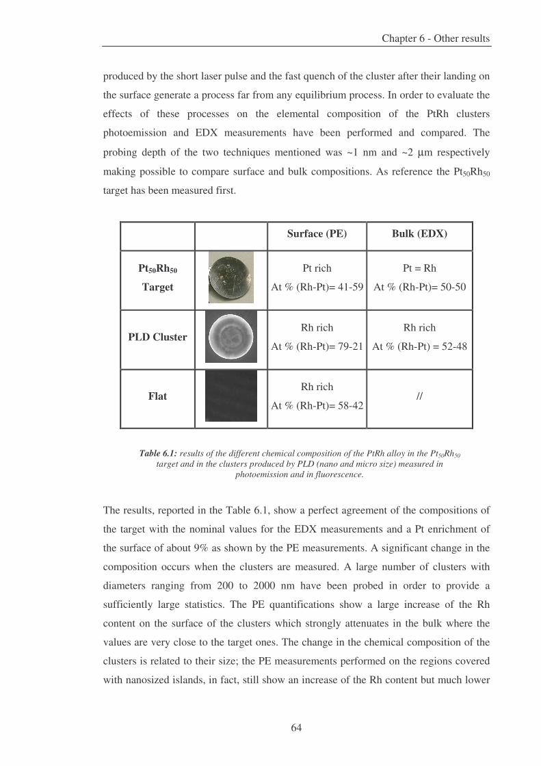
Chapter 6 - Other results
64
produced by the short laser pulse and the fast quench of the cluster after their landing on
the surface generate a process far from any equilibrium process. In order to evaluate the
effects of these processes on the elemental composition of the PtRh clusters
photoemission and EDX measurements have been performed and compared. The
probing depth of the two techniques mentioned was ~1 nm and ~2 µm respectively
making possible to compare surface and bulk compositions. As reference the Pt50Rh50
target has been measured first.
Surface (PE) Bulk (EDX)
Pt50Rh50
Target
Pt rich
At % (Rh-Pt)= 41-59
Pt = Rh
At % (Rh-Pt)= 50-50
PLD Cluster
Rh rich
At % (Rh-Pt)= 79-21
Rh rich
At % (Rh-Pt) = 52-48
Flat
Rh rich
At % (Rh-Pt)= 58-42 //
Table 6.1: results of the different chemical composition of the PtRh alloy in the Pt50Rh50 target and in the clusters produced by PLD (nano and micro size) measured in
photoemission and in fluorescence.
The results, reported in the Table 6.1, show a perfect agreement of the compositions of
the target with the nominal values for the EDX measurements and a Pt enrichment of
the surface of about 9% as shown by the PE measurements. A significant change in the
composition occurs when the clusters are measured. A large number of clusters with
diameters ranging from 200 to 2000 nm have been probed in order to provide a
sufficiently large statistics. The PE quantifications show a large increase of the Rh
content on the surface of the clusters which strongly attenuates in the bulk where the
values are very close to the target ones. The change in the chemical composition of the
clusters is related to their size; the PE measurements performed on the regions covered
with nanosized islands, in fact, still show an increase of the Rh content but much lower

Chapter 6 - Other results
65
than the larger clusters. Due to the low coverage of the nanosized cluster it was not
possible to detect any EDX signal from the related Pt and Rh atoms.
The results obtained unambiguously state a strong dependence of the chemical
composition of the termination layers of the clusters from their size. Cause the spatial
resolution of the SPEM it was not possible to perform a systematic probe of the
stoichiometry between the macro and nanoscopic particles, i.e. to determine if the Pt
surface content linearly decreases with the downsizing of the clusters or if a threshold
dimension exists.
6.2. Morphological changes by annealing
The oxidation and reduction of the PtRh particles was mainly performed while keeping
the sample at 200 °C. This temperature was selected in order to increase the kinetics of
the redox processes without affecting too much other phenomena such as the mass
transport (induced also by the gas phase reactions) or the desorption of the adsorbed
gases. Nevertheless it turned out to be interesting to understand what happened to the
particles when exposed to higher temperatures which could be necessary for several
catalytic reactions. Due to the limited time available only the SEM investigation of the
effects of the temperature on the particles has been performed. Nevertheless the
evolution of the morphology of the particles has revealed unexpected results.
6.2.1. Evolution of the morphology analyzed by SEM
Fig. 6.1 shows one of the PtRh particle selected to probe the temperature effects. This
image corresponds to the particle imaged right after its deposition at room temperature.
As reported in the previous chapters the typical donut-like shape and oriented facets are
well visible.
The sample has been annealed at four different temperatures (400°C, 500°C, 650°C and
850 °C) each kept for 30 minutes. The annealing has been performed in a UHV ambient
with a background pressure of ~1x10⁻⁸ mbar. After each treatment the sample was
removed from the UHV chamber and inserted in the SEM chamber for the
characterization. This step included an exposure of the sample to the ambient pressure
which certainly oxidised the surface.

Chapter 6 - Other results
66
Figure 6.1: SEM image of one cluster deposited by PLD at room temperature before
starting the annealing process.
The effects of the temperature on the particle shown in Fig. 6.1 have been reported in
Fig. 6.2.
a) b)
c)
Figure 6.2: SEM images of the same cluster after three different annealing temperatures. a) 400°C, b) 500°C and c) 650°C.
500 nm
b)
c)

Chapter 6 - Other results
67
After the annealing at 400 °C (Fig. 6.2a) the contrast between the grains appearing on
the surface is more pronounced. Since the sample has been exposed to air prior to the
SEM image, we can not exclude that this change is just due to the oxidation of the
surface. More evident mutations of the surface have been recorded after the annealing at
500 °C and 650 °C. Fig. 6.2b and Fig. 6.2c showing the particle after these two
temperatures, in fact, clearly indicate an increase of the separation between each grain
composing the particle. Boundaries become deeper resembling a canyon-like shape.
This is even more evident in the high resolution maps shown in Fig. 6.3 and 6.4. In spite
of the clear tendency of the boundaries between the grains to become larger and deeper
it is not possible from these images to evaluate to which extent the separation of the
grains occurs while moving inside the particle.
Moreover the top grain visible in Fig. 6.3 seems partially collapsed i.e. at a lower level
with respect to the surrounding regions.
Figure 6.3: high magnification SEM image that shows the collapsing of one facet respect the surrounding others.
200 nm

Chapter 6 - Other results
68
Figure 6.4: high magnification SEM image that shows in particular what happens between the boundaries of the facets.
A dramatic change has been observed after the annealing at 850 °C; the image in Fig.
6.5 shows the particle which appears melted in the outer part while the old structured
Figure 6.5: SEM image of the cluster after annealing at 850°C. The outer part of the cluster is melted and the previous structure exist only in the centre parte.
2 µm
400 nm
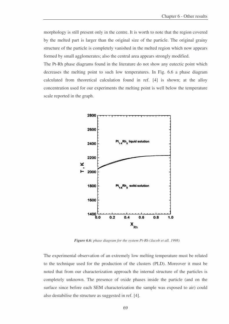
Chapter 6 - Other results
69
morphology is still present only in the centre. It is worth to note that the region covered
by the melted part is larger than the original size of the particle. The original grainy
structure of the particle is completely vanished in the melted region which now appears
formed by small agglomerates; also the central area appears strongly modified.
The Pt-Rh phase diagrams found in the literature do not show any eutectic point which
decreases the melting point to such low temperatures. In Fig. 6.6 a phase diagram
calculated from theoretical calculation found in ref. [4] is shown; at the alloy
concentration used for our experiments the melting point is well below the temperature
scale reported in the graph.
Figure 6.6: phase diagram for the system Pt-Rh (Jacob et all. 1998)
The experimental observation of an extremely low melting temperature must be related
to the technique used for the production of the clusters (PLD). Moreover it must be
noted that from our characterization approach the internal structure of the particles is
completely unknown. The presence of oxide phases inside the particle (and on the
surface since before each SEM characterization the sample was exposed to air) could
also destabilise the structure as suggested in ref. [4].
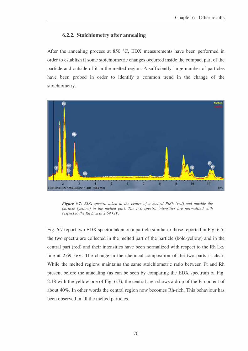
Chapter 6 - Other results
70
6.2.2. Stoichiometry after annealing
After the annealing process at 850 °C, EDX measurements have been performed in
order to establish if some stoichiometric changes occurred inside the compact part of the
particle and outside of it in the melted region. A sufficiently large number of particles
have been probed in order to identify a common trend in the change of the
stoichiometry.
Figure 6.7: EDX spectra taken at the centre of a melted PtRh (red) and outside the particle (yellow) in the melted part. The two spectra intensities are normalized with respect to the Rh L �1 at 2.69 keV.
Fig. 6.7 report two EDX spectra taken on a particle similar to those reported in Fig. 6.5:
the two spectra are collected in the melted part of the particle (bold-yellow) and in the
central part (red) and their intensities have been normalized with respect to the Rh L�1
line at 2.69 keV. The change in the chemical composition of the two parts is clear.
While the melted regions maintains the same stoichiometric ratio between Pt and Rh
present before the annealing (as can be seen by comparing the EDX spectrum of Fig.
2.18 with the yellow one of Fig. 6.7), the central area shows a drop of the Pt content of
about 40%. In other words the central region now becomes Rh-rich. This behaviour has
been observed in all the melted particles.

Chapter 6 - Other results
71
6.3. Photon Beam Induced Reduction
It is well known that the extremely intense focused beam of the SPEM (1018
photons/(mm2 s)) can produce undesired artefacts generated by the interactions of a
large number of photons with the matter. In the reference [5] the main effects have been
reported in detail.
Reduction of oxide samples is one of the most commonly observed photo-chemical
processes [6]. The loss of oxygen, first reported for high valence metal oxides, is driven
by inter-atomic Auger de-excitation after creation of a core hole in the metal ion, which
leads to ejection of O+ ions [7]. Various oxide surfaces can be subjected to photo-
reduction; for example organic samples, simple metal oxides, such as TiO2, Mo oxides,
WO3, CeO2 [8] and complex oxide systems as SrTiO3, bismuthates, etc. [9] have shown
the tendency to reduce after irradiation. The long experience of the SPEM team in
measuring different materials has shown that for the transition metal oxides the
irradiation resistance depends on the actual stoichiometry and the long-range structural
order of the regions irradiated. Disordered oxide phases and thin oxide films with not
well-established structure are usually more vulnerable. As a side effect of the
phenomena in some cases the reduction of the surface could be used to monitor the
stability of the surface phases and can provide important information.
6.3.1. Ageing effects after redox cycles
In the PtRh system a significant photon induced reduction of the oxide phase has been
observed after a procedure aimed to simulate an ageing effect of the particles itself. The
spectra displayed in Fig. 6.8a and Fig. 6.9a show the effect of the focused beam on the
surface of a micron-sized particles oxidised by 765 min of plasma source.
Three successive spectra for the Rh 3d and two following spectra for the Pt 4f show a
weak effect of the beam which tends to reduce the surface. The differences in the shape
of the spectra for the Rh core level are negligible while for the Pt a more pronounced
effect is observed. Afterwards the particle has been exposed to a 48 hours long redox
procedures where time-variable oxidations under atomic oxygen at 200 °C and
reductions with molecular hydrogen (P = 5·10-6 mbar) at the same temperature cycles

Chapter 6 - Other results
72
have been performed. After the same final oxidation of 765 min, the same particle has
been measured.
Figure 6.8: a) Rh3d5/2 spectra taken on a micron-sized cluster after 765 min of oxidation, and b) after 48 hours of redox cycles and a same final oxidation.
Figure 6.9: a) Pt4f7/2 spectra taken on a micron-sized cluster after 765 min of oxidation, and b) after 48 hours of redox cycles and a same final oxidation
The resulting evolution of the spectra is reported in Fig. 6.8b for the Rh 3d and in Fig.
6.9b for the Pt 4f. A clear change in the reduction rate of both elements is visible. As
introduced above this evidence should indicate a dramatic change in the structural order

Chapter 6 - Other results
73
of the oxide phases formed after the “ageing” process applied to the particles. The data
available do not allow a clear correlation between the stoichiometry of the oxide phases
as measured by photoemission before and after the “ageing” which appears similar (the
oxidation condition was in fact the same for both cases). It is preferable at this step just
to show the bare effect of the reduction that to try a speculative analysis following the
fit of the spectra.
6.4. Partial coverage of a single multi-wall carbon nanotube
6.4.1. Carbon Nanotubes (CNTs)
Carbon nanotubes (CNTs) [10] are unique nanosystems with extraordinary mechanical
and electronic properties, which derive from their unusual molecular structure. An ideal
carbon nanotube can be thought of as a single graphite layer (graphene sheet), rolled up
to make a seamless hollow cylinder (Fig. 6.10). These cylinders can be tens of microns
long, with diameters as small as 0.7 nanometres and are closed at both ends by
fullerene-like caps. CNTs having wall thickness of one carbon sheet are named single-
wall carbon nanotubes (SWCNTs). In consequence of the van der Waals interactions
between nanotubes, they often aggregate in large ropes. SWCNTs can be considered as
the building bocks of multi-wall carbon nanotubes (MWCNTs), which consist of a
coaxial array of SWCNTs with increasing diameter. MWCNTs are also usually long
Figure 6.10: rolling up of a grapheme sheet to make a SWCNT
several microns, with the external diameter that ranges from two to several tens of
nanometres, providing very high aspect ratio structures. MWCNTs consist of more than

Chapter 6 - Other results
74
one carbon nanotube arranged concentrically around the axis of the inner tube and
having increasing diameters and different helicities.
The outer diameter of MWCNTs depends on the technique used to grow them; multi-
wall carbon nanotubes either with diameter of a few nanometres and bigger than 100
nanometres can be produced.
Figure 6.11: structure of a multi-walled nanotube.
Many potential applications have been proposed for carbon nanotubes, including
conductive and high-strength composites; energy storage and energy conversion
devices; sensors; field emission displays and radiation sources; hydrogen storage media;
and nanometer-sized semiconductor devices, probes, and interconnects. In addition
CNTs are potentially excellent supports for other materials such as functionalized
coatings or nanostructured catalysts. Their morphological, mechanical, chemical and
electronic properties, in fact, make them suitable for many applications. In this section
the attempts to achieve a partial coverage of a single MWCNT are reported. A confined
patch of metallic coating on a CNT, for instance, opens the possibility for the SPEM for
a detail investigation of phenomena such as the mass transport, the surface and bulk
diffusion, etc.

Chapter 6 - Other results
75
6.4.2. Experimental setups for the partial coverage of a single
MWCNT
In Fig. 6.12 SEM images of high density (109 cm-2) and low density (106 cm-2) aligned
multiwall carbon nanotubes arrays are shown. This configuration of CNTs is ideal for
SPEM experiments. The best lateral resolution achievable in imaging mode (<50 nm)
allows the investigation of the CNT from their side, i.e. in a cross sectional view. In this
way the entire length of a single CNT with diameter down to 50 nm can be analysed.
The density of the array should not exceed a critical number if the goal is to identify
isolated CNT far apart each other.
Figure 6.12: high density (109 cm-2) and low density (106 cm-2) aligned carbon nanotubes arrays. For the high density array the nanotube length is 1-20 µm and the diameter is 30-150 nm, in the case of low density array the length is 1-5 µm and diameter is 50-150 nm.
Different approaches have been followed in order to achieve the result of a partial
coverage (for instance the evaporation of a metal) of a single CNT. Fig. 6.13
summarizes the attempts and results obtained; the first method consists of a grazing
deposition of a metal on the array as shown in the figure. The sample is then cleaved
leaving just the tips of the CNT covered. This approach works well only for highly
dense arrays which results, as visible in the figure, in chaotic SPEM images where it is
difficult to identify a single CNT. Another disadvantage is that the central part of the
CNT remains clean.
The second approach is based on the use of masks with a large number of small holes.
Masks of this type are available commercially but they do not match the ideal
parameters in terms of hole size and hole to hole spacing. It is possible to produce ideal

Chapter 6 - Other results
76
masks following lithographical techniques, but for extended areas the resulting supports
are very fragile.
The best results have been obtained by using home made very narrow slits from
metallic rigid fenditures. With the use of well-known mask alignment techniques it is
possible to realize slits 1-3 µm wide and 1-2 mm long which are not commercially
available. As visible in the SEM picture of Fig. 6.13, different regions of the MWCNT
side wall can be covered.
Figure 6.13: different approaches for a partial of a single CNT 1)The first method consists of a grazing deposition of a metal on the array. The sample is then cleaved
leaving just the tips of the CNT covered. The SPEM image on the right shows the result of this deposition. 2) The second approach is based on the use of available commercially
masks (like sieve membrane) with a large number of small holes. SEM image on the right show the deposition in correspondence of the holes. 3) The third method uses a home
made very narrow slits from metallic rigid fenditures done with lithographical techniques. With the use of well-known mask alignment techniques it is possible to realize
slits 1-3 µm wide and 1-2 mm like in the SEM image on the right.
Fig. 6.14 shows a SPEM picture of a low density array of MWCNTs. Individual
MWCNT with width down to 50 nm can be identified and measured.
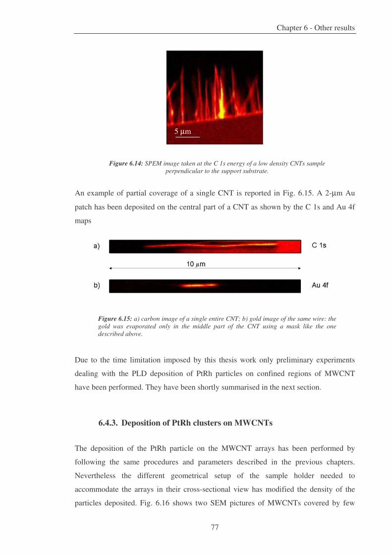
Chapter 6 - Other results
77
Figure 6.14: SPEM image taken at the C 1s energy of a low density CNTs sample perpendicular to the support substrate.
An example of partial coverage of a single CNT is reported in Fig. 6.15. A 2-µm Au
patch has been deposited on the central part of a CNT as shown by the C 1s and Au 4f
maps
Figure 6.15: a) carbon image of a single entire CNT; b) gold image of the same wire: the gold was evaporated only in the middle part of the CNT using a mask like the one described above.
Due to the time limitation imposed by this thesis work only preliminary experiments
dealing with the PLD deposition of PtRh particles on confined regions of MWCNT
have been performed. They have been shortly summarised in the next section.
6.4.3. Deposition of PtRh clusters on MWCNTs
The deposition of the PtRh particle on the MWCNT arrays has been performed by
following the same procedures and parameters described in the previous chapters.
Nevertheless the different geometrical setup of the sample holder needed to
accommodate the arrays in their cross-sectional view has modified the density of the
particles deposited. Fig. 6.16 shows two SEM pictures of MWCNTs covered by few
5 µm

Chapter 6 - Other results
78
PtRh particles. Image a) shows a 50 nm large particle attached to the tip of the MWCNT
while image b) reveals the presence of few nanometre scale particles close to a larger
one attached along the MWCNT side.
a) b)
Figure 6.16: SEM images of nano-sized PtRh clusters deposited on single MWCNT.
Regions where a higher density of particles is present have been found as visible in Fig.
6.17; due to the particular morphology of MWCNTs a very high resolution microscopy
like TEM would be necessary to identify and investigate the smaller clusters in the
nanometre range.
Figure 6.17: two PtRh clusters deposited on a single MWCNT: one at the bottom and one in the middle of the wire.
100 nm
100 nm
100 nm
3 µm

Chapter 6 - Other results
79
References 1 Wouda, P.T.; Nieuwenhuys, B.E.; Schmid, M.; Varga, P. Surface Science 1996, 359,
17-22.
2 Baraldi, A.; Giacomello, D.; Rumiz, L.; Moretuzzo, M.; Lizzit, S.; Buatier De
Mongeot, F.; Paolucci, G.; Kiskinova, M. J. Am. Chem. Soc. 2005, 127, 5671-5674.
3 Zhu, L.; Wang, R.; King, T.S.; DePristo, A. E. Journ of Catalysis 1997, 167, 408-411.
4 Jacob, K.T.; Priya, S.; Waseda, Y. Bull. Mater. Sci. 1998, 21, 99-103.
5 Gregoratti, L.; Mentes, T.O.; Locatelli, A.; Kiskinova, M. Journal of Electron
Spectroscopy and Related Phenomena 2009, 170, 13–18.
6 Ramsier, R.D.; Yates, J.T. Surf. Sci. Rep. 1991, 12, 243, and the references therein.
7 Feibelman, P.J.; Knotek, M.L. Phys. Rev. B 1978, 18, 6531.
8 Locatelli, A.; Pabisiak, T.; Pavlovska, A.; Mentes, T.O.; Aballe, L.; Kiejna, A.; Bauer,
E. J. Phys.: Condens. Matter 2007, 19, 082202.
9 Zakharov, A.A.; Johansson, U.; Leandersson, M.; Nylen, H.; Ovarford, M.; Lindau I.;
Nyholm, R. Phys. Rev. 1997, B56, 5755.
10 Iijima, S. Nature 1991, 354, 56.

Chapter 7 - Conclusions
80
Chapter 7 Conclusions In spite of the progress made, monitoring the local chemical state of a single catalyst
particle and providing a strict morphology control remain unresolved problems even
during preparation of model catalysts. Apart from instrumental limitations to control the
morphology, in fact, there are many reasons that prevent the particles to attain the
predicted equilibrium shape, such as strain at the interface, temperature-induced
reduction in surface energy anisotropy, coalescence during the growth process, etc. In
the case of alloy systems, the complications due to uncertainty regarding metal particle
size, morphology and structure are further exacerbated by added ambiguities concerning
the particle surface composition.
In the present thesis work using a combination of chemical imaging, micro-
spectroscopic and structural methods with sub-micron spatial resolution, we explored
the oxidation of supported PtRh micro- and nano- particles to derive structure-reactivity
and size-reactivity relationships. The most important findings, which are a step towards
bridging the material gap in catalyst research, are listed below.
1. Independently of the particle size Rh oxidises faster than Pt and a thick Rh oxide
layer is formed in the advanced oxidation state. Both Rh2O3 and RhO2
stoichiometric phases form and coexist in the advanced oxidation stage, whereas
the oxidation of Pt is limited only to the top few layers without reaching the
highest PtO2 oxidation phase. In accordance with previous studies for oxidation
of PtRh alloys, the evolution of the Pt 4f and Rh 3d spectra are identical to those
reported during oxidation of Pt and Rh alone, i.e. the two metals preserve their
relative reactivity and there is no indication for formation of a mixed oxide
phase.

Chapter 7 - Conclusions
81
2. The Pt and Rh degrees of oxidation showed marked lateral variations within a
single micro-particle. This inhomogeneity in the oxidation states correlates to the
initial complex surface structure of the micro-particles consisting of facets with
different orientations and degree of surface order, which determines the local
oxidation rate.
3. The oxidation process is accompanied by continuous structural changes and loss
of the ordered atomic structure on the facets. The most advanced oxidation state
is characterised with a disordered surface, concomitant with the observed
coexistence and random distribution of many oxidation phases consisting of
clusters where Rh and Pt have reached different degrees of oxidation.
4. The size-effect is clearly manifested by the higher Pt and Rh oxidation states of
the nano-particles compared to the micro-particles under identical reaction
conditions. However, the more advanced oxidation state attained by the nano-
particles cannot be considered as a simple size effect, since it is obscured by
uncertainty regarding their morphology and structure.
In summary, our findings demonstrate that determining and controlling the particles
morphology, structure and composition and their evolution under reaction conditions is
of the utmost importance. The present results show that changes may occur on very
local microscopic scales resulting in structural and compositional heterogeneity. The
observed compositional complexity of the PtRh particles and the loss of a long range
order under oxidation conditions support the most recent views that the catalytically
active states under operation conditions are not well-defined and ordered stoichiometric
phases but are dynamic states lying often at the boundary between two phases. This also
suggests that in catalytic reactions only fractions of the particle surface can behave as an
active catalyst, i.e. looking for simple size-activity trends on assumption of a known
equilibrium shape, structure and composition is far from the reality. It is the challenge
of the years to come to gain detailed structural knowledge with careful chemical
analysis probing single nano-particles.
Other results have shown that the stoichiometry of the PtRh particles produced by PLD
depends on their size and is different from values reported in the literature for PtRh

Chapter 7 - Conclusions
82
alloy bulk crystals. PLD seems to affect also other parameters such as the phase
diagram of this compound which seems to be present a low melting point. All these
findings that have been only partially addressed stimulate the research on this topic;
additional experiments have been already scheduled to shed light on these and other
aspects still unclear.

List of pubblications
List of publications
Dudin, P., Barinov, A., Dalmiglio, M., Gregoratti, L., Kiskinova, M., Goriachko, A.,
Over, H., “Nanoscale morphology and oxidation of ion-sputtered Rh(110) and
Ru(0001)”, 2008 Journal of Electron Spectroscopy and Related Phenomena 166-167 (1-
3 C), pp. 89-93.
Bhuvana, T., Gregoratti, L., Heun, S., Dalmiglio, M., Kulkarni, G.U., “Electron resist
behavior of pd hexadecanethiolate examined using x-ray photoelectron spectroscopy
with nanometric lateral resolution”, 2009 Langmuir 25 (2), pp. 1259-1264.
Barinov, A., Malcio�lu, O.B., Fabris, S., Sun, T., Gregoratti, L., Dalmiglio, M.,
Kiskinova, M., “Initial stages of oxidation on graphitic surfaces: Photoemission study
and density functional theory calculations”, 2009 Journal of Physical Chemistry C 113
(21), pp. 9009-9013.
Bozzini, B., Dalmiglio, M., De Gaudenzi, G.P., D'Urzo, L., Gregoratti, L., “An
investigation of the corrosion of WC-Co cermets in CN--containing aqueous solutions”.
Part II: Synchrotron-based high lateral-resolution XPS study, 2009 Corrosion Science
51 (8), pp. 1675-1678.
Dalmiglio, M., Amati, M., Gregoratti, L., Mente�, T.O., Niño, M.A., Felisari, L.,
Kiskinova, M., “Oxidation of supported PtRh particles: size and morphology effects”,
Journal of Physical Chemistry C, accepted.

Acknowledgments
First of all, I would like to thank all the former and present colleagues and friends who helped me
during these years and for the very intense and fruitful team work. I am very grateful to dr. Luca
Gregoratti for giving me the opportunity to work in the ESCAmicroscopy group and for his support
and help throughout my research. In fact I accepted to stay here in Trieste and to obtain a PhD title
because of his kindness, humanity and friendliness. It’s not so easy to find people you can work so
serenely with and that who give you understanding and support in a way that allows you to wake up
every morning and go to work with happiness.
Moreover I’m very grateful to all the other people that helped me with their presence, friendship
and competence. In particular I would like to thank the following persons: Alexei Barinov, Matteo
Amati, Majid Kazemian Abyaneh and Maya Kiskinova of the ESCAmicroscopy group, Andrea
Locatelli, Tevfik Onur Mentes, Miguel Angel Nino Orti of the Nanospectroscopy group, Laura
Felisari for the hundreds of SEM images, Denis Scaini and Pietro Parisse for the AFM
measurements, Mauro Prasciolu for the lithographic works, Annalisa Boscaino and Giusy Palma
for all the time we spent together in the canteen and at the coffee machine, and all the other
colleagues that I met at Elettra.
Last but not least I want to thank all my friends in Trieste for their liking, kindness and support:
these three years flied away very fast thanks to all the good time that I spent with them. And of
course I would like to thank my parents who sustained me with comprehension, affection and
nearness although I was far from them.