Embed Size (px)
Citation preview

1
Oxidation of copper during physical sputtering deposition mechanism
avoidance and utilization
Jiangbin Su12 Yang Liu1 Meiping Jiang1ǂ Xianfang Zhu2
1 Experiment Center of Electronic Science and Technology amp Department of Electronic Science and
Engineering School of Mathematics and Physics Changzhou University Changzhou 213164 PR China
2 China-Australia Joint Laboratory for Functional Nanomaterials amp Physics Department Xiamen
University Xiamen 361005 PR China
ǂ Corresponding authors Tel +86 051986330300 E-mail addresses jbsucczueducn (JB Su)
mpjiangcczueducn (MP Jiang)
Abstract In this paper oxidation of Cu during physical sputtering deposition in a high purity and low
pressure Ar atmosphere without introducing O2 gas flow was studied systemically It was found that
various flexible Cu-based films such as pure Cu films CuCu2O composite films pure Cu2O films
Cu2OCuO composite films and pure CuO films could be obtained by simply adjusting deposition
parameters Electrical and optical testing results showed that the achieved pure Cu films and CuCu2O
composite films both presented an intriguing combination of metal and semiconductor characteristics For
pure Cu films the electrical resistivity and energy gap are ~10-4 Ωcm and 154 eV respectively while for
CuCu2O composite films the electrical resistivity and energy gap are ~10-5 Ωcm and 248 eV
respectively It is expected that such Cu-based films with a superior conductivity and a solar-window
bandgap may have fascinating potential applications such as in high electron mobility transistors
electrodes and solar cells Further the oxidation mechanisms of Cu under different deposition parameters
and the main O2 source during physical sputtering deposition were also explored
2
Keywords Cu oxidation physical sputtering deposition high vacuum electrical resistivity energy
gap
1 Introduction
Copper (Cu) thin films have been regarded as the next material to replace aluminum (Al) metallization in
ultra-large-scale integrated circuits (ULSIC) due to their noticeable advantages such as low resistivity and
superior electro-migration resistance [12] In literature the study of Cu films has been generally centered
on the optimization of film properties under various deposition techniques [3-5] for specific applications
such as interconnection candidate of ULSIC However we should further note that the surface of Cu films
especially of nanoscale size is susceptible to oxygen and gets oxidized spontaneously not only when
exposing to the air but also during film growing For the former cause we can package the Cu
interconnection-based chips to keep away from the air and water as much as possible for the latter cause
we often try to deposit Cu films in a pre-pumped high vacuum chamber with (eg physical sputtering) or
without (eg thermal or electron-beam evaporation) a high-purity working rare gas such as argon (Ar) In
physical sputtering deposition the base pressure of chamber is generally up to 10-4 - 10-5 Pa and the
working gas is often of 99999 wt high purity [5-6] As presented in this paper however we
experimentally demonstrate that even under such a high pure condition Cu films can be partially or even
totally oxidized during film growth (see further) Obviously such undesirable oxidation would influence
the performance stability and lifetime of the Cu films used as interconnection in ULSIC to a certain
extent or even severely Thus study on the oxidation of Cu during physical sputtering deposition is
crucial not only to mechanism understanding but also to practical avoidance of the undesirable oxidation
3
On the other hand as the most common two kinds of Cu oxides tenorite (CuO) and cuprite (Cu2O)
have attracted much attention due to their applications in low-cost solar cells and other optoelectronic
devices [7-8] However there is still little research focused on the fabrication and properties of Cu-based
composite films such as CuCu2O films which comprise of metal and semiconductor components and
may have different properties and potential applications In addition the commonly-used sputtering
deposition technology for the fabrication of CuO and Cu2O is reactive sputtering deposition [8] rather
than physical sputtering deposition as applied in this paper Different from physical sputtering deposition
additional reactive gas flow such as high pure oxygen (O2) is used in reactive sputtering deposition to
supply O2 source for the oxidation reactions of sputtering material atoms However according to our
calculation results (see further) it is found that the residual O2 in the pre-pumped high vacuum chamber
(50times10-4 Pa) and the high purity and low pressure sputtering gas Ar (99999 wt 01 Pa) is sufficient
for full oxidation of sputtered Cu atoms Thus it is expected that physical sputtering of Cu in high pure
Ar atmosphere can also be utilized to fabricate Cu-based oxide films Chandra et al [9] have demonstrated
that Cu2O thin films could be synthesized without using external O2 source but at a high pressure of inert
gas (at and above 100 mTorr) Although the O2 source during high pressure sputtering was not revealed in
Ref [9] different from our low pressure case it should originate from the impurity of inert gas rather
than the residual O2 in the pre-pumped high vacuum according to our calculation Furthermore the
parameter-dependent oxidation behavior and mechanism of Cu during physical sputtering deposition
especially at a commonly-used low pressure have not been studied systematically
With the above considerations in this paper we particularly studied the oxidation of Cu during
physical sputtering deposition in a high purity and low pressure Ar atmosphere Our calculation results
4
showed that the main O2 source for the oxidation of Cu was the residual O2 in chamber vacuum which
originated from the limited pre-pumped vacuum along with the impurity of working gas Thermodynamic
and kinetic analyses demonstrated that the oxidation of Cu could work spontaneously but depended on
deposition parameters greatly Further we studied the fabrication of Cu-based oxide films by physical
sputtering deposition and their electrical and optical properties It was found that various flexible
Cu-based films such as pure Cu films CuCu2O composite films pure Cu2O films Cu2OCuO composite
films and pure CuO films could be obtained by simply controlling the deposition parameters Electrical
and optical testing results showed that the achieved Cu2O films displayed a typical semiconductor
characteristic while the achieved pure Cu thin films and CuCu2O composite films both presented an
intriguing combination of metal and semiconductor characteristics
2 Experimental
All Cu and Cu-based samples shown in this paper were deposited on glass slides in a JGP500A balanced
magnetron sputtering system The Cu target was of 9999 wt purity and the glass slide substrates were
cleaned following standard cleaning procedures The distance between the target and the substrates was
set to be ~15 cm A base pressure of 50times10-4 Pa was achieved by a turbo-molecular pump backed by a
mechanical pump Before each deposition a pre-sputtering of 10 min was regularly performed to remove
the possible oxide layers on the target surface Then physical sputtering deposition was carried out at a
pressure of 01 Pa in a high pure Ar atmosphere (purity 99999 wt flow rate 15 sccm) To explore the
oxidation behavior of Cu during film growing we designed five typical sets of experiments by changing
deposition parameters such as work mode (direct current and radio frequency DC amp RF) sputtering
power density substrate bias voltage and substrate temperature As different sputtering deposition
5
conditions are often with different deposition rates the deposition rate and time were monitored by a
quartz crystal oscillator near the substrate to make each set comparable The detailed values of these
parameters can be found in Table 1 Since the glass slide substrates are mainly composed of silicon and
oxygen elements the common energy dispersive X-ray spectroscopy (EDX) analysis is not suitable for
the detection of oxygen element in the glass slide-substrated thin films Alternatively a powder X-ray
diffractometer (XRD RIGAKU DMax 2500 PC) was applied subsequently for the composition or phase
characterization of the as-deposited films This is because the sputter deposits always tend to crystallize
during deposition even at room temperature which can be well detected by XRD Further electrical and
optical testing experiments were carried out by using a four-point probe instrument (SDY-4) and an
ultraviolet-visible (UV-Vis) spectrophotometer (SHIMADZU UV-2450)
3 Results and discussion
The XRD patterns in Figs 1-5 show the compositions or phases of the physically sputtered Cu deposits
under different deposition parameters including work mode (DC amp RF) sputtering power density p
substrate bias voltage Vs and substrate temperature Ts (1) For different work modes as shown in Fig 1
the deposit achieved by DC mode displays a pure composition of Cu while the deposit achieved by RF
mode displays a mixed oxidation composition of CuOCu2O (2) for different sputtering power densities P
as shown in Fig 2 the deposit obtained at p = 219 Wcm2 exhibits a pure composition of Cu while the
deposit obtained at p = 088 Wcm2 exhibits a partial oxidation composition of CuCu2O (3) for different
work modes and sputtering power density as shown in Fig 3 the deposit gained at RF 176 Wcm2
demonstrates a single oxidation composition of Cu2O while the deposit gained at DC 088 Wcm2
demonstrates a partial oxidation composition of CuCu2O (4) for different substrate bias voltages Vs as
6
shown in Fig 4 the deposit gotten at Vs = 0 V presents a mixed oxidation composition of CuOCu2O
while the deposit gotten at Vs = -100 V presents a single oxidation composition of CuO (5) for different
substrate temperatures Ts as shown in Fig 5 the deposit acquired at Ts = 20 degC (room temperature) shows
a pure composition of Cu while the deposit acquired at Ts = 400 degC shows a partial oxidation composition
of CuCu2O The deposition parameters and the corresponding XRD analysis results are further listed in
Table 1 The same experiments were repeated several times and similar XRD results were obtained We
can thus conclude that DC sputtering mode high sputtering power density low substrate bias voltage and
low substrate temperature are more suitable for the fabrication of pure Cu films on the contrary RF
sputtering mode low sputtering power density high substrate bias voltage and high substrate temperature
are more possible to prepare Cu films with Cu2O component or even total Cu2O andor CuO films
As experimentally demonstrated above partial or even entire sputtered Cu atoms can be oxidized
into Cu2O or CuO during physical sputtering deposition Generally there are three possible O2 sources
applied for the oxidation of Cu (1) the impurity of 9999 wt Cu target (2) the O2 molecules adsorbed
on the glass slide surface (3) the limited pre-pumped vacuum (50times10-4 Pa) and the impurity of 99999
wt and 01 Pa Ar working gas Alternatively someone may think that the release of O2 adsorbed on the
inner wall of chamber would also supply the O2 Actually such release of O2 should be and is considered
as one part of the 3rd source (the remained O2 in pre-pumped vacuum) because the O2 after releasing
would come into the chamber vacuum
In the following we analyze and compare the respective contents of O and Cu at the above
mentioned three specified locations For the 1st possible source assuming that all the impurity in the Cu
target is O element the atomic ratio of O and Cu is 12500 So small is the O content that we can
7
completely ignore its influence For the 2nd possible source we compare the surface density of adsorbed
O2 on glass slide surface with that of as-deposited Cu atomic layer According to ref [10] we know that
the adsorption of O2 on glass (total surface 1966 cm2) at a pressure of 07 torr is 063 mm3 (volume at 20
degC and 760 mm pressure) Since the quantity of adsorbed gas is proportional to the pressure at low
pressure [10] the surface density of adsorbed O2 on glass slide surface in our case is about 22times105
atomscm2 In comparison the surface density of as-deposited Cu about 1014 atomscm2 is much larger
Accordingly we can ignore the little influence of adsorbed O2 on the surface of glass slide substrates For
the 3rd possible source the partial oxygen pressure in chamber vacuum (including two parts one is from
the pre-pumped high vacuum and the other one is from the high pure working gas Ar) is about 95times10-5
Pa In this calculation for the sake of simplicity we assume that the volume fraction of O2 in the
pre-pumped high vacuum is 21 which is similar to the composition of air Due to the low pressure we
can apply the State Equation of Ideal Gas (ie PV = nRT) to obtain the concentration of O2 in chamber
vacuum Our calculation result is about 48times1010 atomscm3 On the other hand provided no or little
reflection occurs for simplicity during the incident Cu flux striking the substrate we can achieve the
following equation
vM
Nvn AdCu
Cu
(1)
where Cun is the concentration of incident Cu atoms near the glass substrate Cu is the density of Cu
film about 84 gcm3 [6] dv is the deposition rate of Cu atoms with a typical value of 001 - 02 nms in
this paper AN is the Avogadro constant v is the average velocity of travelling Cu atoms before
reaching the substrate M is the atomic weight of Cu After a detailed calculation as ref [11] we find
that the average retained kinetic energy of a sputtered Cu atom in this work is 124 eV Thus the average
8
velocity v of Cu atoms near the substrate is about 19times103 ms According to Eq (1) the concentration of
incident Cu atoms near the substrate is about 108 - 109 atomscm3 Since the concentration of O2 in
chamber vacuum is larger than that of Cu atoms near the substrate (48times1010 vs 108 - 109 atomscm3) the
residual O2 is sufficient in quantity and should be the main source for the oxidation of Cu atoms during
physical sputtering deposition What is more part of sputtered Cu atoms may be preferentially oxidized
on the target surface before travelling to the substrate The comparison of O and Cu contents at the above
mentioned three different locations is further shown in Table 2
Based on thermodynamic data the reactions between Cu and O2 are as follows
OCugOCu 22 )(2
12 (2)
CuOgOCu )(2
12 (3)
CuOgOOCu )(4
1
2
122 (4)
The changes in free energy at room temperature given by Eqs (2-4) are -14769 -12812 and -5427
kJmol-1 respectively all of which are much lower than zero It indicates that Cu can be oxidized
spontaneously at room temperature under an atmosphere containing sufficient O2 We should further note
that different from the oxidation of bulk Cu the oxidation of gaseous Cu atoms during sputtering
deposition would be greatly enhanced due to a much higher energy and a much more full exposure to O2
In addition the oxidation of Cu into Cu2O (Eq (2)) seems the easiest to occur due to the biggest change
in free energy In spite of this Cu and Cu2O can also be oxidized or further oxidized into CuO due to the
changes in free energy given by Eqs (3-4) are both much lower than zero
Thermodynamically as demonstrated above the sputtered Cu atoms can react spontaneously at room
temperature with the sufficient O2 molecules retained in vacuum Nevertheless not all the sputter deposits
9
are Cu2O or CuO as expected which are observed to be dependent kinetically on the deposition
parameters such as work modes sputtering power density substrate bias voltage and substrate
temperature (see Figs 1-5 or Table 1) In the following we discuss the influences of the above deposition
parameters on the oxidation of Cu atoms during physical sputtering deposition
For different work modes DC mode relative to RF mode leads to a much higher deposition rate (see
Set 1 Table 1) Similarly as shown in Set 2 of Table 1 larger sputtering power density could also cause a
much higher deposition rate Generally speaking a higher deposition rate could shorten the required
deposition time which would prevent Cu atoms from sufficiently exposing to O2 This should be the main
reason why DC mode with large sputtering power density tends to achieve pure Cu films while RF mode
or small sputtering power density tends to form Cu films with Cu2O component or even total Cu2O andor
CuO films However relative to DC 088 Wcm2 as shown in Set 3 of Table 1 RF 176 Wcm2 with a
higher deposition rate (0045 vs 003 nms) and a shorter period of deposition time (15 vs 2 h) seems to
obtain a more fully oxidized film (Cu2O vs CuCu2O) inversely It indicates that there may be another
factor influencing the oxidation of Cu besides the deposition rate and time It is expected that the different
work modes DC and RF result in such different oxidation effect As is known to all similar to the
working gas Ar the residual O2 between two electrodes would be ionized into plasma (including O2+ e-
O O2 etc) during sputtering For DC sputtering the O2+ travels directionally to the target surface
(cathode) While for RF sputtering the O2+ travels back and forth between two electrodes which may
increase the opportunity of reaction with the sputtered Cu atoms For different substrate bias voltage or
different substrate temperature as shown in Sets 4 and 5 of Table 1 the work mode deposition rate and
time between two typical experiments are the same or nearly the same However the achieved sputter
10
deposits are more fully oxidized under higher substrate bias voltage (CuO vs CuOCu2O) or higher
substrate temperature (CuCu2O vs Cu) This is probably due to the additional energy supplied to Cu
atoms and O2 molecules under higher substrate bias voltage or higher substrate temperature promotes the
oxidation of Cu or further oxidation of Cu2O
Although we can try to pump the chamber vacuum to less than 10-6 Pa to avoid the undesirable
oxidation as much as possible it would greatly increase the fabrication cost and time What is worse the
common high-pure working gas Ar is typically of 99999 wt purity which would also introduce
unexpected O2 and make it infeasible Alternatively in this paper DC mode with a high sputtering power
density such as 219 Wcm2 is demonstrated to be an efficient and low-cost method to deposit pure Cu
films Further it is also demonstrated that we can deposit Cu films with Cu2O component or Cu2O andor
CuO films by adjusting the deposition parameters For example DC mode with a low sputtering power
density such as 088 Wcm2 at room temperature can be applied to fabricate CuCu2O composite films
DC mode with a high sputtering power density such as 219 Wcm2 at 400degC can also be applied to
fabricate CuCu2O composite films RF mode with a strong magnetic field of ~6 kGs (see caption of
Table 1) and a sputtering power density of 176 Wcm2 is suitable for the fabrication of Cu2O films while
RF mode with a relatively weaker magnetic field of ~45 kGs (see caption of Table 1) and a sputtering
power density of 219 Wcm2 is suitable for the fabrication of CuO films (with substrate bias voltage) or
Cu2OCuO composite films (without substrate bias voltage)
Table 3 and Fig 6 show the electrical resistivity and the (Ahv)2 - hv curves of the achieved Cu2O Cu
and CuCu2O films respectively For Cu2O film the electrical resistivity is larger than 100 Ωcm and the
energy gap is 206 eV which shows a typical semiconductor characteristic for pure Cu film it displays an
11
intriguing combination of metal and semiconductor characteristics with a low electrical resistivity of
~10-4 Ωcm and a narrow bandgap of 154 eV while for CuCu2O composite film even more intriguing it
also displays a combination of metal and semiconductor characteristics with a much lower electrical
resistivity of ~10-5 Ωcm and a much wider bandgap of 248 eV It is expected that quantum size effect of
two-dimensional thin films (and the massive doping of Cu in Cu2O for CuCu2O composite film) results
in such interesting phenomena although the detailed mechanisms are still unclear In spite of this such
pure Cu films and CuCu2O composite films with a low electrical resistivity and a bandgap at the solar
window may have fascinating potential applications such as in high electron mobility transistors [12]
electrodes [13] and solar cells [14-15]
4 Conclusions
In this work the oxidation of Cu during physical sputtering deposition was studied by varying the
deposition parameters including work mode sputtering power density substrate bias voltage and
substrate temperature Our calculation results showed that the main O2 source for the oxidation of Cu was
the residual O2 in chamber vacuum which originated from the limited pre-pumped vacuum (50times10-4 Pa)
along with the impurity of 99999 wt and 01 Pa working gas Ar It was demonstrated that DC mode
with a large sputtering power density such as 219 Wcm2 at room temperature tended to deposit pure Cu
films while DC mode with a small sputtering power density such as 088 Wcm2 or at an elevated
temperature of 400degC tended to deposit CuCu2O composite films It was also demonstrated that RF mode
normally with a low deposition rate was more suitable for the fabrication of Cu2O andor CuO films
rather than pure Cu or CuCu2O composite films Electrical and optical testing results showed that the
achieved Cu2O films displayed a typical semiconductor characteristic with an electrical resistivity larger
12
than 100 Ωcm and an energy gap of 206 eV However the achieved pure Cu films and CuCu2O
composite films both presented an intriguing combination of metal and semiconductor characteristics For
pure Cu films the electrical resistivity and energy gap are ~10-4 Ωcm and 154 eV respectively while for
CuCu2O composite films the electrical resistivity and energy gap are ~10-5 Ωcm and 248 eV
respectively Based on these findings it provided not only an effective route to avoid the oxidation of
sputtered Cu atoms during physical sputtering deposition but also a flexible and low-cost new method to
prepare various Cu-based oxide films
Acknowledgements
The authors thank Honghong Wang Dingjuan Pan and Dan Jin at School of Mathematics and Physics
Changzhou University for their experimental assistance
References
[1] CW Park RW Vook Activation energy for electromigration in Cu films Appl Phys Lett 59 (1991)
175-177
[2] SP Murarka RJ Gutmann Advanced multilayer metallization schemes with copper as
interconnection metal Thin Solid Films 236 (1993) 257-266
[3] RA Roy JJ Cuomo DS Yee Control of microstructure and properties of copper films using
ion-assisted deposition J Vac Sci Technol A 6 (1988) 1621-1626
[4] WM Holber JS Logan HJ Grabarz et al Copper deposition by electron cyclotron resonance
plasma J Vac Sci Technol A 11 (1993) 2903-2910
[5] KY Chan TY Tou BS Teo Effects of substrate temperature on electrical and structural properties
13
of copper thin films Microelectron J 37 (2006) 930-937
[6] HM Choi SK Choi O Aderson et al Influence of film density on residual stress and resistivity for
Cu thin films deposited by bias sputtering Thin Solid Films 358 (2000) 202-205
[7] B Balamurugan BR Mehta Optical and structural properties of nanocrystalline copper oxide thin
films prepared by activated reactive evaporation Thin Solid Films 396 (2001) 90-96
[8] A Parretta MK Jayaraj AD Nocera et al Electrical and optical properties of copper oxide films
prepared by reactive RF magnetron sputtering Phys Stat Sol 155 (1996) 399-404
[9] R Chandra P Taneja P Ayyub Optical properties of transparent nanocrystalline Cu2O thin films
synthesized by high pressure gas sputtering Nanostruct Mater 11 (1999) 505-512
[10] I Langmuir The adsorption of gases on plane surfaces of glass mica and platinum J Am Chem
Soc 40 (1918) 1361-1403
[11] JB Su XX Li MP Jiang et al Layer-plus-wire growth of copper by small incident angle
deposition Mater Lett 92 (2013) 304-307
[12] S Balendhran J Deng JZ Ou et al Enhanced charge carrier mobility in two-dimensional high
dielectric molybdenum oxide Adv Mater 25 (2013) 109-114
[13] S Anandan X Wen S Yang Room temperature growth of CuO nanorod arrays on copper and their
application as a cathode in dye-sensitized solar cells Mater Chem Phys 93 (2005) 35-40
[14] JJ Loferski Theoretical considerations governing the choice of the optimum semiconductor for
photovoltaic solar energy conversion J Appl Phys 27 (1956) 777-784
[15] H Tanaka T Shimakawa T Miyata et al Effect of AZO film deposition conditions on the
photovoltaic properties of AZO-Cu2O heterojunctions Appl Surf Sci 244 (2005) 568-572
14
Table captions
Table 1 Five typical sets of experiments under different deposition parameters where p is the sputtering
power density Vs is the substrate bias voltage Ts is the substrate temperature vd and t are the deposition
rate and time respectively Remark Different from the RF mode in Sets 1 and 4 the RFrsquo mode in Set 3
with a stronger magnetic field (~6 vs ~45 kGs) causes a higher deposition rate (0045 vs 002 nms)
even under a lower sputtering power density (176 vs 219 Wcm2)
Table 2 The contents of O and Cu elements at different locations
Table 3 Electrical resistivity of the achieved Cu2O Cu and CuCu2O films
15
Figure captions
Fig 1 XRD patterns showing the composition of the Cu deposits obtained under different work modes
(Set 1 DC amp RF 219 Wcm2)
Fig 2 XRD patterns showing the composition of the Cu deposits obtained under different sputtering
power density (Set 2 p = 219 Wcm2 088 Wcm2)
Fig 3 XRD patterns showing the composition of the Cu deposits obtained under different work modes
and sputtering power density (Set 3 RF 176 Wcm2 DC 088 Wcm2)
Fig 4 XRD patterns showing the composition of the Cu deposits obtained under different substrate bias
voltage (Set 4 Vs = 0 V -100 V)
Fig 5 XRD patterns showing the composition of the Cu deposits obtained under different substrate
temperature (Set 5 Ts = 20 degC 400 degC)
Fig 6 (Ahv)2 - hv curves of the achieved (a) Cu2O (b) Cu and (c) CuCu2O films
1
Tables
Table 1
Sets Work mode p (Wcm2) Vs (V) Ts (degC) vd (nms) t (h s) Phase
1
DC
RF
219
219
0
0
20
20
~02 155s
~002 15h
Cu
CuO Cu2O
2
DC
DC
219
088
0
0
20
20
~02 288s
~003 2h
Cu
Cu Cu2O
3
RFrsquo
DC
176
088
0
0
20
20
~0045 15h
~003 2h
Cu2O
Cu Cu2O
4
RF
RF
219
219
0
-100
20
20
~002 15h
~002 15h
CuO Cu2O
CuO
5
DC
DC
219
219
0
0
20
400
~02 155s
~02 155s
Cu
Cu Cu2O
Table 2
Locations O Cu
1st Cu target (ratio) 1 2500
2nd glass slide surface 22times105 atomscm2 ~1014 atomscm2
3rd vacuum near substrate 48times1010 atomscm3 ~108 - 109 atomscm3
2
Table 3
Samples Electrical Resistivity
Cu2O film gt100 Ωcm
Cu film ~10-4 Ωcm
CuCu2O film ~10-5 Ωcm
Figures
Fig 1
Fig 2
DC 219 Wcm2
CuO
(002)
Cu (111)
Cu2O (111)
RF 219 Wcm2
Cu2O (200)
p = 088 Wcm2
Cu (111)
Cu (200)
p = 219 Wcm2Cu2O (111)
Fig 3
Fig 4
Vs = -100 V
CuO (002)
CuO (002)Cu2O (111)
Cu2O (200)
Vs = 0 V
DC 088 Wcm2
RF 176 Wcm2
Cu (111)
Cu (200)
Cu2O (111)
Cu2O (111)
Cu2O (200)Cu2O (220)
Fig 5
Fig 6
(a)
Ts = 20 degC
Ts = 400 degC
Cu (111)
Cu (200)
Cu2O
(111)
(b)
(c)

2
Keywords Cu oxidation physical sputtering deposition high vacuum electrical resistivity energy
gap
1 Introduction
Copper (Cu) thin films have been regarded as the next material to replace aluminum (Al) metallization in
ultra-large-scale integrated circuits (ULSIC) due to their noticeable advantages such as low resistivity and
superior electro-migration resistance [12] In literature the study of Cu films has been generally centered
on the optimization of film properties under various deposition techniques [3-5] for specific applications
such as interconnection candidate of ULSIC However we should further note that the surface of Cu films
especially of nanoscale size is susceptible to oxygen and gets oxidized spontaneously not only when
exposing to the air but also during film growing For the former cause we can package the Cu
interconnection-based chips to keep away from the air and water as much as possible for the latter cause
we often try to deposit Cu films in a pre-pumped high vacuum chamber with (eg physical sputtering) or
without (eg thermal or electron-beam evaporation) a high-purity working rare gas such as argon (Ar) In
physical sputtering deposition the base pressure of chamber is generally up to 10-4 - 10-5 Pa and the
working gas is often of 99999 wt high purity [5-6] As presented in this paper however we
experimentally demonstrate that even under such a high pure condition Cu films can be partially or even
totally oxidized during film growth (see further) Obviously such undesirable oxidation would influence
the performance stability and lifetime of the Cu films used as interconnection in ULSIC to a certain
extent or even severely Thus study on the oxidation of Cu during physical sputtering deposition is
crucial not only to mechanism understanding but also to practical avoidance of the undesirable oxidation
3
On the other hand as the most common two kinds of Cu oxides tenorite (CuO) and cuprite (Cu2O)
have attracted much attention due to their applications in low-cost solar cells and other optoelectronic
devices [7-8] However there is still little research focused on the fabrication and properties of Cu-based
composite films such as CuCu2O films which comprise of metal and semiconductor components and
may have different properties and potential applications In addition the commonly-used sputtering
deposition technology for the fabrication of CuO and Cu2O is reactive sputtering deposition [8] rather
than physical sputtering deposition as applied in this paper Different from physical sputtering deposition
additional reactive gas flow such as high pure oxygen (O2) is used in reactive sputtering deposition to
supply O2 source for the oxidation reactions of sputtering material atoms However according to our
calculation results (see further) it is found that the residual O2 in the pre-pumped high vacuum chamber
(50times10-4 Pa) and the high purity and low pressure sputtering gas Ar (99999 wt 01 Pa) is sufficient
for full oxidation of sputtered Cu atoms Thus it is expected that physical sputtering of Cu in high pure
Ar atmosphere can also be utilized to fabricate Cu-based oxide films Chandra et al [9] have demonstrated
that Cu2O thin films could be synthesized without using external O2 source but at a high pressure of inert
gas (at and above 100 mTorr) Although the O2 source during high pressure sputtering was not revealed in
Ref [9] different from our low pressure case it should originate from the impurity of inert gas rather
than the residual O2 in the pre-pumped high vacuum according to our calculation Furthermore the
parameter-dependent oxidation behavior and mechanism of Cu during physical sputtering deposition
especially at a commonly-used low pressure have not been studied systematically
With the above considerations in this paper we particularly studied the oxidation of Cu during
physical sputtering deposition in a high purity and low pressure Ar atmosphere Our calculation results
4
showed that the main O2 source for the oxidation of Cu was the residual O2 in chamber vacuum which
originated from the limited pre-pumped vacuum along with the impurity of working gas Thermodynamic
and kinetic analyses demonstrated that the oxidation of Cu could work spontaneously but depended on
deposition parameters greatly Further we studied the fabrication of Cu-based oxide films by physical
sputtering deposition and their electrical and optical properties It was found that various flexible
Cu-based films such as pure Cu films CuCu2O composite films pure Cu2O films Cu2OCuO composite
films and pure CuO films could be obtained by simply controlling the deposition parameters Electrical
and optical testing results showed that the achieved Cu2O films displayed a typical semiconductor
characteristic while the achieved pure Cu thin films and CuCu2O composite films both presented an
intriguing combination of metal and semiconductor characteristics
2 Experimental
All Cu and Cu-based samples shown in this paper were deposited on glass slides in a JGP500A balanced
magnetron sputtering system The Cu target was of 9999 wt purity and the glass slide substrates were
cleaned following standard cleaning procedures The distance between the target and the substrates was
set to be ~15 cm A base pressure of 50times10-4 Pa was achieved by a turbo-molecular pump backed by a
mechanical pump Before each deposition a pre-sputtering of 10 min was regularly performed to remove
the possible oxide layers on the target surface Then physical sputtering deposition was carried out at a
pressure of 01 Pa in a high pure Ar atmosphere (purity 99999 wt flow rate 15 sccm) To explore the
oxidation behavior of Cu during film growing we designed five typical sets of experiments by changing
deposition parameters such as work mode (direct current and radio frequency DC amp RF) sputtering
power density substrate bias voltage and substrate temperature As different sputtering deposition
5
conditions are often with different deposition rates the deposition rate and time were monitored by a
quartz crystal oscillator near the substrate to make each set comparable The detailed values of these
parameters can be found in Table 1 Since the glass slide substrates are mainly composed of silicon and
oxygen elements the common energy dispersive X-ray spectroscopy (EDX) analysis is not suitable for
the detection of oxygen element in the glass slide-substrated thin films Alternatively a powder X-ray
diffractometer (XRD RIGAKU DMax 2500 PC) was applied subsequently for the composition or phase
characterization of the as-deposited films This is because the sputter deposits always tend to crystallize
during deposition even at room temperature which can be well detected by XRD Further electrical and
optical testing experiments were carried out by using a four-point probe instrument (SDY-4) and an
ultraviolet-visible (UV-Vis) spectrophotometer (SHIMADZU UV-2450)
3 Results and discussion
The XRD patterns in Figs 1-5 show the compositions or phases of the physically sputtered Cu deposits
under different deposition parameters including work mode (DC amp RF) sputtering power density p
substrate bias voltage Vs and substrate temperature Ts (1) For different work modes as shown in Fig 1
the deposit achieved by DC mode displays a pure composition of Cu while the deposit achieved by RF
mode displays a mixed oxidation composition of CuOCu2O (2) for different sputtering power densities P
as shown in Fig 2 the deposit obtained at p = 219 Wcm2 exhibits a pure composition of Cu while the
deposit obtained at p = 088 Wcm2 exhibits a partial oxidation composition of CuCu2O (3) for different
work modes and sputtering power density as shown in Fig 3 the deposit gained at RF 176 Wcm2
demonstrates a single oxidation composition of Cu2O while the deposit gained at DC 088 Wcm2
demonstrates a partial oxidation composition of CuCu2O (4) for different substrate bias voltages Vs as
6
shown in Fig 4 the deposit gotten at Vs = 0 V presents a mixed oxidation composition of CuOCu2O
while the deposit gotten at Vs = -100 V presents a single oxidation composition of CuO (5) for different
substrate temperatures Ts as shown in Fig 5 the deposit acquired at Ts = 20 degC (room temperature) shows
a pure composition of Cu while the deposit acquired at Ts = 400 degC shows a partial oxidation composition
of CuCu2O The deposition parameters and the corresponding XRD analysis results are further listed in
Table 1 The same experiments were repeated several times and similar XRD results were obtained We
can thus conclude that DC sputtering mode high sputtering power density low substrate bias voltage and
low substrate temperature are more suitable for the fabrication of pure Cu films on the contrary RF
sputtering mode low sputtering power density high substrate bias voltage and high substrate temperature
are more possible to prepare Cu films with Cu2O component or even total Cu2O andor CuO films
As experimentally demonstrated above partial or even entire sputtered Cu atoms can be oxidized
into Cu2O or CuO during physical sputtering deposition Generally there are three possible O2 sources
applied for the oxidation of Cu (1) the impurity of 9999 wt Cu target (2) the O2 molecules adsorbed
on the glass slide surface (3) the limited pre-pumped vacuum (50times10-4 Pa) and the impurity of 99999
wt and 01 Pa Ar working gas Alternatively someone may think that the release of O2 adsorbed on the
inner wall of chamber would also supply the O2 Actually such release of O2 should be and is considered
as one part of the 3rd source (the remained O2 in pre-pumped vacuum) because the O2 after releasing
would come into the chamber vacuum
In the following we analyze and compare the respective contents of O and Cu at the above
mentioned three specified locations For the 1st possible source assuming that all the impurity in the Cu
target is O element the atomic ratio of O and Cu is 12500 So small is the O content that we can
7
completely ignore its influence For the 2nd possible source we compare the surface density of adsorbed
O2 on glass slide surface with that of as-deposited Cu atomic layer According to ref [10] we know that
the adsorption of O2 on glass (total surface 1966 cm2) at a pressure of 07 torr is 063 mm3 (volume at 20
degC and 760 mm pressure) Since the quantity of adsorbed gas is proportional to the pressure at low
pressure [10] the surface density of adsorbed O2 on glass slide surface in our case is about 22times105
atomscm2 In comparison the surface density of as-deposited Cu about 1014 atomscm2 is much larger
Accordingly we can ignore the little influence of adsorbed O2 on the surface of glass slide substrates For
the 3rd possible source the partial oxygen pressure in chamber vacuum (including two parts one is from
the pre-pumped high vacuum and the other one is from the high pure working gas Ar) is about 95times10-5
Pa In this calculation for the sake of simplicity we assume that the volume fraction of O2 in the
pre-pumped high vacuum is 21 which is similar to the composition of air Due to the low pressure we
can apply the State Equation of Ideal Gas (ie PV = nRT) to obtain the concentration of O2 in chamber
vacuum Our calculation result is about 48times1010 atomscm3 On the other hand provided no or little
reflection occurs for simplicity during the incident Cu flux striking the substrate we can achieve the
following equation
vM
Nvn AdCu
Cu
(1)
where Cun is the concentration of incident Cu atoms near the glass substrate Cu is the density of Cu
film about 84 gcm3 [6] dv is the deposition rate of Cu atoms with a typical value of 001 - 02 nms in
this paper AN is the Avogadro constant v is the average velocity of travelling Cu atoms before
reaching the substrate M is the atomic weight of Cu After a detailed calculation as ref [11] we find
that the average retained kinetic energy of a sputtered Cu atom in this work is 124 eV Thus the average
8
velocity v of Cu atoms near the substrate is about 19times103 ms According to Eq (1) the concentration of
incident Cu atoms near the substrate is about 108 - 109 atomscm3 Since the concentration of O2 in
chamber vacuum is larger than that of Cu atoms near the substrate (48times1010 vs 108 - 109 atomscm3) the
residual O2 is sufficient in quantity and should be the main source for the oxidation of Cu atoms during
physical sputtering deposition What is more part of sputtered Cu atoms may be preferentially oxidized
on the target surface before travelling to the substrate The comparison of O and Cu contents at the above
mentioned three different locations is further shown in Table 2
Based on thermodynamic data the reactions between Cu and O2 are as follows
OCugOCu 22 )(2
12 (2)
CuOgOCu )(2
12 (3)
CuOgOOCu )(4
1
2
122 (4)
The changes in free energy at room temperature given by Eqs (2-4) are -14769 -12812 and -5427
kJmol-1 respectively all of which are much lower than zero It indicates that Cu can be oxidized
spontaneously at room temperature under an atmosphere containing sufficient O2 We should further note
that different from the oxidation of bulk Cu the oxidation of gaseous Cu atoms during sputtering
deposition would be greatly enhanced due to a much higher energy and a much more full exposure to O2
In addition the oxidation of Cu into Cu2O (Eq (2)) seems the easiest to occur due to the biggest change
in free energy In spite of this Cu and Cu2O can also be oxidized or further oxidized into CuO due to the
changes in free energy given by Eqs (3-4) are both much lower than zero
Thermodynamically as demonstrated above the sputtered Cu atoms can react spontaneously at room
temperature with the sufficient O2 molecules retained in vacuum Nevertheless not all the sputter deposits
9
are Cu2O or CuO as expected which are observed to be dependent kinetically on the deposition
parameters such as work modes sputtering power density substrate bias voltage and substrate
temperature (see Figs 1-5 or Table 1) In the following we discuss the influences of the above deposition
parameters on the oxidation of Cu atoms during physical sputtering deposition
For different work modes DC mode relative to RF mode leads to a much higher deposition rate (see
Set 1 Table 1) Similarly as shown in Set 2 of Table 1 larger sputtering power density could also cause a
much higher deposition rate Generally speaking a higher deposition rate could shorten the required
deposition time which would prevent Cu atoms from sufficiently exposing to O2 This should be the main
reason why DC mode with large sputtering power density tends to achieve pure Cu films while RF mode
or small sputtering power density tends to form Cu films with Cu2O component or even total Cu2O andor
CuO films However relative to DC 088 Wcm2 as shown in Set 3 of Table 1 RF 176 Wcm2 with a
higher deposition rate (0045 vs 003 nms) and a shorter period of deposition time (15 vs 2 h) seems to
obtain a more fully oxidized film (Cu2O vs CuCu2O) inversely It indicates that there may be another
factor influencing the oxidation of Cu besides the deposition rate and time It is expected that the different
work modes DC and RF result in such different oxidation effect As is known to all similar to the
working gas Ar the residual O2 between two electrodes would be ionized into plasma (including O2+ e-
O O2 etc) during sputtering For DC sputtering the O2+ travels directionally to the target surface
(cathode) While for RF sputtering the O2+ travels back and forth between two electrodes which may
increase the opportunity of reaction with the sputtered Cu atoms For different substrate bias voltage or
different substrate temperature as shown in Sets 4 and 5 of Table 1 the work mode deposition rate and
time between two typical experiments are the same or nearly the same However the achieved sputter
10
deposits are more fully oxidized under higher substrate bias voltage (CuO vs CuOCu2O) or higher
substrate temperature (CuCu2O vs Cu) This is probably due to the additional energy supplied to Cu
atoms and O2 molecules under higher substrate bias voltage or higher substrate temperature promotes the
oxidation of Cu or further oxidation of Cu2O
Although we can try to pump the chamber vacuum to less than 10-6 Pa to avoid the undesirable
oxidation as much as possible it would greatly increase the fabrication cost and time What is worse the
common high-pure working gas Ar is typically of 99999 wt purity which would also introduce
unexpected O2 and make it infeasible Alternatively in this paper DC mode with a high sputtering power
density such as 219 Wcm2 is demonstrated to be an efficient and low-cost method to deposit pure Cu
films Further it is also demonstrated that we can deposit Cu films with Cu2O component or Cu2O andor
CuO films by adjusting the deposition parameters For example DC mode with a low sputtering power
density such as 088 Wcm2 at room temperature can be applied to fabricate CuCu2O composite films
DC mode with a high sputtering power density such as 219 Wcm2 at 400degC can also be applied to
fabricate CuCu2O composite films RF mode with a strong magnetic field of ~6 kGs (see caption of
Table 1) and a sputtering power density of 176 Wcm2 is suitable for the fabrication of Cu2O films while
RF mode with a relatively weaker magnetic field of ~45 kGs (see caption of Table 1) and a sputtering
power density of 219 Wcm2 is suitable for the fabrication of CuO films (with substrate bias voltage) or
Cu2OCuO composite films (without substrate bias voltage)
Table 3 and Fig 6 show the electrical resistivity and the (Ahv)2 - hv curves of the achieved Cu2O Cu
and CuCu2O films respectively For Cu2O film the electrical resistivity is larger than 100 Ωcm and the
energy gap is 206 eV which shows a typical semiconductor characteristic for pure Cu film it displays an
11
intriguing combination of metal and semiconductor characteristics with a low electrical resistivity of
~10-4 Ωcm and a narrow bandgap of 154 eV while for CuCu2O composite film even more intriguing it
also displays a combination of metal and semiconductor characteristics with a much lower electrical
resistivity of ~10-5 Ωcm and a much wider bandgap of 248 eV It is expected that quantum size effect of
two-dimensional thin films (and the massive doping of Cu in Cu2O for CuCu2O composite film) results
in such interesting phenomena although the detailed mechanisms are still unclear In spite of this such
pure Cu films and CuCu2O composite films with a low electrical resistivity and a bandgap at the solar
window may have fascinating potential applications such as in high electron mobility transistors [12]
electrodes [13] and solar cells [14-15]
4 Conclusions
In this work the oxidation of Cu during physical sputtering deposition was studied by varying the
deposition parameters including work mode sputtering power density substrate bias voltage and
substrate temperature Our calculation results showed that the main O2 source for the oxidation of Cu was
the residual O2 in chamber vacuum which originated from the limited pre-pumped vacuum (50times10-4 Pa)
along with the impurity of 99999 wt and 01 Pa working gas Ar It was demonstrated that DC mode
with a large sputtering power density such as 219 Wcm2 at room temperature tended to deposit pure Cu
films while DC mode with a small sputtering power density such as 088 Wcm2 or at an elevated
temperature of 400degC tended to deposit CuCu2O composite films It was also demonstrated that RF mode
normally with a low deposition rate was more suitable for the fabrication of Cu2O andor CuO films
rather than pure Cu or CuCu2O composite films Electrical and optical testing results showed that the
achieved Cu2O films displayed a typical semiconductor characteristic with an electrical resistivity larger
12
than 100 Ωcm and an energy gap of 206 eV However the achieved pure Cu films and CuCu2O
composite films both presented an intriguing combination of metal and semiconductor characteristics For
pure Cu films the electrical resistivity and energy gap are ~10-4 Ωcm and 154 eV respectively while for
CuCu2O composite films the electrical resistivity and energy gap are ~10-5 Ωcm and 248 eV
respectively Based on these findings it provided not only an effective route to avoid the oxidation of
sputtered Cu atoms during physical sputtering deposition but also a flexible and low-cost new method to
prepare various Cu-based oxide films
Acknowledgements
The authors thank Honghong Wang Dingjuan Pan and Dan Jin at School of Mathematics and Physics
Changzhou University for their experimental assistance
References
[1] CW Park RW Vook Activation energy for electromigration in Cu films Appl Phys Lett 59 (1991)
175-177
[2] SP Murarka RJ Gutmann Advanced multilayer metallization schemes with copper as
interconnection metal Thin Solid Films 236 (1993) 257-266
[3] RA Roy JJ Cuomo DS Yee Control of microstructure and properties of copper films using
ion-assisted deposition J Vac Sci Technol A 6 (1988) 1621-1626
[4] WM Holber JS Logan HJ Grabarz et al Copper deposition by electron cyclotron resonance
plasma J Vac Sci Technol A 11 (1993) 2903-2910
[5] KY Chan TY Tou BS Teo Effects of substrate temperature on electrical and structural properties
13
of copper thin films Microelectron J 37 (2006) 930-937
[6] HM Choi SK Choi O Aderson et al Influence of film density on residual stress and resistivity for
Cu thin films deposited by bias sputtering Thin Solid Films 358 (2000) 202-205
[7] B Balamurugan BR Mehta Optical and structural properties of nanocrystalline copper oxide thin
films prepared by activated reactive evaporation Thin Solid Films 396 (2001) 90-96
[8] A Parretta MK Jayaraj AD Nocera et al Electrical and optical properties of copper oxide films
prepared by reactive RF magnetron sputtering Phys Stat Sol 155 (1996) 399-404
[9] R Chandra P Taneja P Ayyub Optical properties of transparent nanocrystalline Cu2O thin films
synthesized by high pressure gas sputtering Nanostruct Mater 11 (1999) 505-512
[10] I Langmuir The adsorption of gases on plane surfaces of glass mica and platinum J Am Chem
Soc 40 (1918) 1361-1403
[11] JB Su XX Li MP Jiang et al Layer-plus-wire growth of copper by small incident angle
deposition Mater Lett 92 (2013) 304-307
[12] S Balendhran J Deng JZ Ou et al Enhanced charge carrier mobility in two-dimensional high
dielectric molybdenum oxide Adv Mater 25 (2013) 109-114
[13] S Anandan X Wen S Yang Room temperature growth of CuO nanorod arrays on copper and their
application as a cathode in dye-sensitized solar cells Mater Chem Phys 93 (2005) 35-40
[14] JJ Loferski Theoretical considerations governing the choice of the optimum semiconductor for
photovoltaic solar energy conversion J Appl Phys 27 (1956) 777-784
[15] H Tanaka T Shimakawa T Miyata et al Effect of AZO film deposition conditions on the
photovoltaic properties of AZO-Cu2O heterojunctions Appl Surf Sci 244 (2005) 568-572
14
Table captions
Table 1 Five typical sets of experiments under different deposition parameters where p is the sputtering
power density Vs is the substrate bias voltage Ts is the substrate temperature vd and t are the deposition
rate and time respectively Remark Different from the RF mode in Sets 1 and 4 the RFrsquo mode in Set 3
with a stronger magnetic field (~6 vs ~45 kGs) causes a higher deposition rate (0045 vs 002 nms)
even under a lower sputtering power density (176 vs 219 Wcm2)
Table 2 The contents of O and Cu elements at different locations
Table 3 Electrical resistivity of the achieved Cu2O Cu and CuCu2O films
15
Figure captions
Fig 1 XRD patterns showing the composition of the Cu deposits obtained under different work modes
(Set 1 DC amp RF 219 Wcm2)
Fig 2 XRD patterns showing the composition of the Cu deposits obtained under different sputtering
power density (Set 2 p = 219 Wcm2 088 Wcm2)
Fig 3 XRD patterns showing the composition of the Cu deposits obtained under different work modes
and sputtering power density (Set 3 RF 176 Wcm2 DC 088 Wcm2)
Fig 4 XRD patterns showing the composition of the Cu deposits obtained under different substrate bias
voltage (Set 4 Vs = 0 V -100 V)
Fig 5 XRD patterns showing the composition of the Cu deposits obtained under different substrate
temperature (Set 5 Ts = 20 degC 400 degC)
Fig 6 (Ahv)2 - hv curves of the achieved (a) Cu2O (b) Cu and (c) CuCu2O films
1
Tables
Table 1
Sets Work mode p (Wcm2) Vs (V) Ts (degC) vd (nms) t (h s) Phase
1
DC
RF
219
219
0
0
20
20
~02 155s
~002 15h
Cu
CuO Cu2O
2
DC
DC
219
088
0
0
20
20
~02 288s
~003 2h
Cu
Cu Cu2O
3
RFrsquo
DC
176
088
0
0
20
20
~0045 15h
~003 2h
Cu2O
Cu Cu2O
4
RF
RF
219
219
0
-100
20
20
~002 15h
~002 15h
CuO Cu2O
CuO
5
DC
DC
219
219
0
0
20
400
~02 155s
~02 155s
Cu
Cu Cu2O
Table 2
Locations O Cu
1st Cu target (ratio) 1 2500
2nd glass slide surface 22times105 atomscm2 ~1014 atomscm2
3rd vacuum near substrate 48times1010 atomscm3 ~108 - 109 atomscm3
2
Table 3
Samples Electrical Resistivity
Cu2O film gt100 Ωcm
Cu film ~10-4 Ωcm
CuCu2O film ~10-5 Ωcm
Figures
Fig 1
Fig 2
DC 219 Wcm2
CuO
(002)
Cu (111)
Cu2O (111)
RF 219 Wcm2
Cu2O (200)
p = 088 Wcm2
Cu (111)
Cu (200)
p = 219 Wcm2Cu2O (111)
Fig 3
Fig 4
Vs = -100 V
CuO (002)
CuO (002)Cu2O (111)
Cu2O (200)
Vs = 0 V
DC 088 Wcm2
RF 176 Wcm2
Cu (111)
Cu (200)
Cu2O (111)
Cu2O (111)
Cu2O (200)Cu2O (220)
Fig 5
Fig 6
(a)
Ts = 20 degC
Ts = 400 degC
Cu (111)
Cu (200)
Cu2O
(111)
(b)
(c)

3
On the other hand as the most common two kinds of Cu oxides tenorite (CuO) and cuprite (Cu2O)
have attracted much attention due to their applications in low-cost solar cells and other optoelectronic
devices [7-8] However there is still little research focused on the fabrication and properties of Cu-based
composite films such as CuCu2O films which comprise of metal and semiconductor components and
may have different properties and potential applications In addition the commonly-used sputtering
deposition technology for the fabrication of CuO and Cu2O is reactive sputtering deposition [8] rather
than physical sputtering deposition as applied in this paper Different from physical sputtering deposition
additional reactive gas flow such as high pure oxygen (O2) is used in reactive sputtering deposition to
supply O2 source for the oxidation reactions of sputtering material atoms However according to our
calculation results (see further) it is found that the residual O2 in the pre-pumped high vacuum chamber
(50times10-4 Pa) and the high purity and low pressure sputtering gas Ar (99999 wt 01 Pa) is sufficient
for full oxidation of sputtered Cu atoms Thus it is expected that physical sputtering of Cu in high pure
Ar atmosphere can also be utilized to fabricate Cu-based oxide films Chandra et al [9] have demonstrated
that Cu2O thin films could be synthesized without using external O2 source but at a high pressure of inert
gas (at and above 100 mTorr) Although the O2 source during high pressure sputtering was not revealed in
Ref [9] different from our low pressure case it should originate from the impurity of inert gas rather
than the residual O2 in the pre-pumped high vacuum according to our calculation Furthermore the
parameter-dependent oxidation behavior and mechanism of Cu during physical sputtering deposition
especially at a commonly-used low pressure have not been studied systematically
With the above considerations in this paper we particularly studied the oxidation of Cu during
physical sputtering deposition in a high purity and low pressure Ar atmosphere Our calculation results
4
showed that the main O2 source for the oxidation of Cu was the residual O2 in chamber vacuum which
originated from the limited pre-pumped vacuum along with the impurity of working gas Thermodynamic
and kinetic analyses demonstrated that the oxidation of Cu could work spontaneously but depended on
deposition parameters greatly Further we studied the fabrication of Cu-based oxide films by physical
sputtering deposition and their electrical and optical properties It was found that various flexible
Cu-based films such as pure Cu films CuCu2O composite films pure Cu2O films Cu2OCuO composite
films and pure CuO films could be obtained by simply controlling the deposition parameters Electrical
and optical testing results showed that the achieved Cu2O films displayed a typical semiconductor
characteristic while the achieved pure Cu thin films and CuCu2O composite films both presented an
intriguing combination of metal and semiconductor characteristics
2 Experimental
All Cu and Cu-based samples shown in this paper were deposited on glass slides in a JGP500A balanced
magnetron sputtering system The Cu target was of 9999 wt purity and the glass slide substrates were
cleaned following standard cleaning procedures The distance between the target and the substrates was
set to be ~15 cm A base pressure of 50times10-4 Pa was achieved by a turbo-molecular pump backed by a
mechanical pump Before each deposition a pre-sputtering of 10 min was regularly performed to remove
the possible oxide layers on the target surface Then physical sputtering deposition was carried out at a
pressure of 01 Pa in a high pure Ar atmosphere (purity 99999 wt flow rate 15 sccm) To explore the
oxidation behavior of Cu during film growing we designed five typical sets of experiments by changing
deposition parameters such as work mode (direct current and radio frequency DC amp RF) sputtering
power density substrate bias voltage and substrate temperature As different sputtering deposition
5
conditions are often with different deposition rates the deposition rate and time were monitored by a
quartz crystal oscillator near the substrate to make each set comparable The detailed values of these
parameters can be found in Table 1 Since the glass slide substrates are mainly composed of silicon and
oxygen elements the common energy dispersive X-ray spectroscopy (EDX) analysis is not suitable for
the detection of oxygen element in the glass slide-substrated thin films Alternatively a powder X-ray
diffractometer (XRD RIGAKU DMax 2500 PC) was applied subsequently for the composition or phase
characterization of the as-deposited films This is because the sputter deposits always tend to crystallize
during deposition even at room temperature which can be well detected by XRD Further electrical and
optical testing experiments were carried out by using a four-point probe instrument (SDY-4) and an
ultraviolet-visible (UV-Vis) spectrophotometer (SHIMADZU UV-2450)
3 Results and discussion
The XRD patterns in Figs 1-5 show the compositions or phases of the physically sputtered Cu deposits
under different deposition parameters including work mode (DC amp RF) sputtering power density p
substrate bias voltage Vs and substrate temperature Ts (1) For different work modes as shown in Fig 1
the deposit achieved by DC mode displays a pure composition of Cu while the deposit achieved by RF
mode displays a mixed oxidation composition of CuOCu2O (2) for different sputtering power densities P
as shown in Fig 2 the deposit obtained at p = 219 Wcm2 exhibits a pure composition of Cu while the
deposit obtained at p = 088 Wcm2 exhibits a partial oxidation composition of CuCu2O (3) for different
work modes and sputtering power density as shown in Fig 3 the deposit gained at RF 176 Wcm2
demonstrates a single oxidation composition of Cu2O while the deposit gained at DC 088 Wcm2
demonstrates a partial oxidation composition of CuCu2O (4) for different substrate bias voltages Vs as
6
shown in Fig 4 the deposit gotten at Vs = 0 V presents a mixed oxidation composition of CuOCu2O
while the deposit gotten at Vs = -100 V presents a single oxidation composition of CuO (5) for different
substrate temperatures Ts as shown in Fig 5 the deposit acquired at Ts = 20 degC (room temperature) shows
a pure composition of Cu while the deposit acquired at Ts = 400 degC shows a partial oxidation composition
of CuCu2O The deposition parameters and the corresponding XRD analysis results are further listed in
Table 1 The same experiments were repeated several times and similar XRD results were obtained We
can thus conclude that DC sputtering mode high sputtering power density low substrate bias voltage and
low substrate temperature are more suitable for the fabrication of pure Cu films on the contrary RF
sputtering mode low sputtering power density high substrate bias voltage and high substrate temperature
are more possible to prepare Cu films with Cu2O component or even total Cu2O andor CuO films
As experimentally demonstrated above partial or even entire sputtered Cu atoms can be oxidized
into Cu2O or CuO during physical sputtering deposition Generally there are three possible O2 sources
applied for the oxidation of Cu (1) the impurity of 9999 wt Cu target (2) the O2 molecules adsorbed
on the glass slide surface (3) the limited pre-pumped vacuum (50times10-4 Pa) and the impurity of 99999
wt and 01 Pa Ar working gas Alternatively someone may think that the release of O2 adsorbed on the
inner wall of chamber would also supply the O2 Actually such release of O2 should be and is considered
as one part of the 3rd source (the remained O2 in pre-pumped vacuum) because the O2 after releasing
would come into the chamber vacuum
In the following we analyze and compare the respective contents of O and Cu at the above
mentioned three specified locations For the 1st possible source assuming that all the impurity in the Cu
target is O element the atomic ratio of O and Cu is 12500 So small is the O content that we can
7
completely ignore its influence For the 2nd possible source we compare the surface density of adsorbed
O2 on glass slide surface with that of as-deposited Cu atomic layer According to ref [10] we know that
the adsorption of O2 on glass (total surface 1966 cm2) at a pressure of 07 torr is 063 mm3 (volume at 20
degC and 760 mm pressure) Since the quantity of adsorbed gas is proportional to the pressure at low
pressure [10] the surface density of adsorbed O2 on glass slide surface in our case is about 22times105
atomscm2 In comparison the surface density of as-deposited Cu about 1014 atomscm2 is much larger
Accordingly we can ignore the little influence of adsorbed O2 on the surface of glass slide substrates For
the 3rd possible source the partial oxygen pressure in chamber vacuum (including two parts one is from
the pre-pumped high vacuum and the other one is from the high pure working gas Ar) is about 95times10-5
Pa In this calculation for the sake of simplicity we assume that the volume fraction of O2 in the
pre-pumped high vacuum is 21 which is similar to the composition of air Due to the low pressure we
can apply the State Equation of Ideal Gas (ie PV = nRT) to obtain the concentration of O2 in chamber
vacuum Our calculation result is about 48times1010 atomscm3 On the other hand provided no or little
reflection occurs for simplicity during the incident Cu flux striking the substrate we can achieve the
following equation
vM
Nvn AdCu
Cu
(1)
where Cun is the concentration of incident Cu atoms near the glass substrate Cu is the density of Cu
film about 84 gcm3 [6] dv is the deposition rate of Cu atoms with a typical value of 001 - 02 nms in
this paper AN is the Avogadro constant v is the average velocity of travelling Cu atoms before
reaching the substrate M is the atomic weight of Cu After a detailed calculation as ref [11] we find
that the average retained kinetic energy of a sputtered Cu atom in this work is 124 eV Thus the average
8
velocity v of Cu atoms near the substrate is about 19times103 ms According to Eq (1) the concentration of
incident Cu atoms near the substrate is about 108 - 109 atomscm3 Since the concentration of O2 in
chamber vacuum is larger than that of Cu atoms near the substrate (48times1010 vs 108 - 109 atomscm3) the
residual O2 is sufficient in quantity and should be the main source for the oxidation of Cu atoms during
physical sputtering deposition What is more part of sputtered Cu atoms may be preferentially oxidized
on the target surface before travelling to the substrate The comparison of O and Cu contents at the above
mentioned three different locations is further shown in Table 2
Based on thermodynamic data the reactions between Cu and O2 are as follows
OCugOCu 22 )(2
12 (2)
CuOgOCu )(2
12 (3)
CuOgOOCu )(4
1
2
122 (4)
The changes in free energy at room temperature given by Eqs (2-4) are -14769 -12812 and -5427
kJmol-1 respectively all of which are much lower than zero It indicates that Cu can be oxidized
spontaneously at room temperature under an atmosphere containing sufficient O2 We should further note
that different from the oxidation of bulk Cu the oxidation of gaseous Cu atoms during sputtering
deposition would be greatly enhanced due to a much higher energy and a much more full exposure to O2
In addition the oxidation of Cu into Cu2O (Eq (2)) seems the easiest to occur due to the biggest change
in free energy In spite of this Cu and Cu2O can also be oxidized or further oxidized into CuO due to the
changes in free energy given by Eqs (3-4) are both much lower than zero
Thermodynamically as demonstrated above the sputtered Cu atoms can react spontaneously at room
temperature with the sufficient O2 molecules retained in vacuum Nevertheless not all the sputter deposits
9
are Cu2O or CuO as expected which are observed to be dependent kinetically on the deposition
parameters such as work modes sputtering power density substrate bias voltage and substrate
temperature (see Figs 1-5 or Table 1) In the following we discuss the influences of the above deposition
parameters on the oxidation of Cu atoms during physical sputtering deposition
For different work modes DC mode relative to RF mode leads to a much higher deposition rate (see
Set 1 Table 1) Similarly as shown in Set 2 of Table 1 larger sputtering power density could also cause a
much higher deposition rate Generally speaking a higher deposition rate could shorten the required
deposition time which would prevent Cu atoms from sufficiently exposing to O2 This should be the main
reason why DC mode with large sputtering power density tends to achieve pure Cu films while RF mode
or small sputtering power density tends to form Cu films with Cu2O component or even total Cu2O andor
CuO films However relative to DC 088 Wcm2 as shown in Set 3 of Table 1 RF 176 Wcm2 with a
higher deposition rate (0045 vs 003 nms) and a shorter period of deposition time (15 vs 2 h) seems to
obtain a more fully oxidized film (Cu2O vs CuCu2O) inversely It indicates that there may be another
factor influencing the oxidation of Cu besides the deposition rate and time It is expected that the different
work modes DC and RF result in such different oxidation effect As is known to all similar to the
working gas Ar the residual O2 between two electrodes would be ionized into plasma (including O2+ e-
O O2 etc) during sputtering For DC sputtering the O2+ travels directionally to the target surface
(cathode) While for RF sputtering the O2+ travels back and forth between two electrodes which may
increase the opportunity of reaction with the sputtered Cu atoms For different substrate bias voltage or
different substrate temperature as shown in Sets 4 and 5 of Table 1 the work mode deposition rate and
time between two typical experiments are the same or nearly the same However the achieved sputter
10
deposits are more fully oxidized under higher substrate bias voltage (CuO vs CuOCu2O) or higher
substrate temperature (CuCu2O vs Cu) This is probably due to the additional energy supplied to Cu
atoms and O2 molecules under higher substrate bias voltage or higher substrate temperature promotes the
oxidation of Cu or further oxidation of Cu2O
Although we can try to pump the chamber vacuum to less than 10-6 Pa to avoid the undesirable
oxidation as much as possible it would greatly increase the fabrication cost and time What is worse the
common high-pure working gas Ar is typically of 99999 wt purity which would also introduce
unexpected O2 and make it infeasible Alternatively in this paper DC mode with a high sputtering power
density such as 219 Wcm2 is demonstrated to be an efficient and low-cost method to deposit pure Cu
films Further it is also demonstrated that we can deposit Cu films with Cu2O component or Cu2O andor
CuO films by adjusting the deposition parameters For example DC mode with a low sputtering power
density such as 088 Wcm2 at room temperature can be applied to fabricate CuCu2O composite films
DC mode with a high sputtering power density such as 219 Wcm2 at 400degC can also be applied to
fabricate CuCu2O composite films RF mode with a strong magnetic field of ~6 kGs (see caption of
Table 1) and a sputtering power density of 176 Wcm2 is suitable for the fabrication of Cu2O films while
RF mode with a relatively weaker magnetic field of ~45 kGs (see caption of Table 1) and a sputtering
power density of 219 Wcm2 is suitable for the fabrication of CuO films (with substrate bias voltage) or
Cu2OCuO composite films (without substrate bias voltage)
Table 3 and Fig 6 show the electrical resistivity and the (Ahv)2 - hv curves of the achieved Cu2O Cu
and CuCu2O films respectively For Cu2O film the electrical resistivity is larger than 100 Ωcm and the
energy gap is 206 eV which shows a typical semiconductor characteristic for pure Cu film it displays an
11
intriguing combination of metal and semiconductor characteristics with a low electrical resistivity of
~10-4 Ωcm and a narrow bandgap of 154 eV while for CuCu2O composite film even more intriguing it
also displays a combination of metal and semiconductor characteristics with a much lower electrical
resistivity of ~10-5 Ωcm and a much wider bandgap of 248 eV It is expected that quantum size effect of
two-dimensional thin films (and the massive doping of Cu in Cu2O for CuCu2O composite film) results
in such interesting phenomena although the detailed mechanisms are still unclear In spite of this such
pure Cu films and CuCu2O composite films with a low electrical resistivity and a bandgap at the solar
window may have fascinating potential applications such as in high electron mobility transistors [12]
electrodes [13] and solar cells [14-15]
4 Conclusions
In this work the oxidation of Cu during physical sputtering deposition was studied by varying the
deposition parameters including work mode sputtering power density substrate bias voltage and
substrate temperature Our calculation results showed that the main O2 source for the oxidation of Cu was
the residual O2 in chamber vacuum which originated from the limited pre-pumped vacuum (50times10-4 Pa)
along with the impurity of 99999 wt and 01 Pa working gas Ar It was demonstrated that DC mode
with a large sputtering power density such as 219 Wcm2 at room temperature tended to deposit pure Cu
films while DC mode with a small sputtering power density such as 088 Wcm2 or at an elevated
temperature of 400degC tended to deposit CuCu2O composite films It was also demonstrated that RF mode
normally with a low deposition rate was more suitable for the fabrication of Cu2O andor CuO films
rather than pure Cu or CuCu2O composite films Electrical and optical testing results showed that the
achieved Cu2O films displayed a typical semiconductor characteristic with an electrical resistivity larger
12
than 100 Ωcm and an energy gap of 206 eV However the achieved pure Cu films and CuCu2O
composite films both presented an intriguing combination of metal and semiconductor characteristics For
pure Cu films the electrical resistivity and energy gap are ~10-4 Ωcm and 154 eV respectively while for
CuCu2O composite films the electrical resistivity and energy gap are ~10-5 Ωcm and 248 eV
respectively Based on these findings it provided not only an effective route to avoid the oxidation of
sputtered Cu atoms during physical sputtering deposition but also a flexible and low-cost new method to
prepare various Cu-based oxide films
Acknowledgements
The authors thank Honghong Wang Dingjuan Pan and Dan Jin at School of Mathematics and Physics
Changzhou University for their experimental assistance
References
[1] CW Park RW Vook Activation energy for electromigration in Cu films Appl Phys Lett 59 (1991)
175-177
[2] SP Murarka RJ Gutmann Advanced multilayer metallization schemes with copper as
interconnection metal Thin Solid Films 236 (1993) 257-266
[3] RA Roy JJ Cuomo DS Yee Control of microstructure and properties of copper films using
ion-assisted deposition J Vac Sci Technol A 6 (1988) 1621-1626
[4] WM Holber JS Logan HJ Grabarz et al Copper deposition by electron cyclotron resonance
plasma J Vac Sci Technol A 11 (1993) 2903-2910
[5] KY Chan TY Tou BS Teo Effects of substrate temperature on electrical and structural properties
13
of copper thin films Microelectron J 37 (2006) 930-937
[6] HM Choi SK Choi O Aderson et al Influence of film density on residual stress and resistivity for
Cu thin films deposited by bias sputtering Thin Solid Films 358 (2000) 202-205
[7] B Balamurugan BR Mehta Optical and structural properties of nanocrystalline copper oxide thin
films prepared by activated reactive evaporation Thin Solid Films 396 (2001) 90-96
[8] A Parretta MK Jayaraj AD Nocera et al Electrical and optical properties of copper oxide films
prepared by reactive RF magnetron sputtering Phys Stat Sol 155 (1996) 399-404
[9] R Chandra P Taneja P Ayyub Optical properties of transparent nanocrystalline Cu2O thin films
synthesized by high pressure gas sputtering Nanostruct Mater 11 (1999) 505-512
[10] I Langmuir The adsorption of gases on plane surfaces of glass mica and platinum J Am Chem
Soc 40 (1918) 1361-1403
[11] JB Su XX Li MP Jiang et al Layer-plus-wire growth of copper by small incident angle
deposition Mater Lett 92 (2013) 304-307
[12] S Balendhran J Deng JZ Ou et al Enhanced charge carrier mobility in two-dimensional high
dielectric molybdenum oxide Adv Mater 25 (2013) 109-114
[13] S Anandan X Wen S Yang Room temperature growth of CuO nanorod arrays on copper and their
application as a cathode in dye-sensitized solar cells Mater Chem Phys 93 (2005) 35-40
[14] JJ Loferski Theoretical considerations governing the choice of the optimum semiconductor for
photovoltaic solar energy conversion J Appl Phys 27 (1956) 777-784
[15] H Tanaka T Shimakawa T Miyata et al Effect of AZO film deposition conditions on the
photovoltaic properties of AZO-Cu2O heterojunctions Appl Surf Sci 244 (2005) 568-572
14
Table captions
Table 1 Five typical sets of experiments under different deposition parameters where p is the sputtering
power density Vs is the substrate bias voltage Ts is the substrate temperature vd and t are the deposition
rate and time respectively Remark Different from the RF mode in Sets 1 and 4 the RFrsquo mode in Set 3
with a stronger magnetic field (~6 vs ~45 kGs) causes a higher deposition rate (0045 vs 002 nms)
even under a lower sputtering power density (176 vs 219 Wcm2)
Table 2 The contents of O and Cu elements at different locations
Table 3 Electrical resistivity of the achieved Cu2O Cu and CuCu2O films
15
Figure captions
Fig 1 XRD patterns showing the composition of the Cu deposits obtained under different work modes
(Set 1 DC amp RF 219 Wcm2)
Fig 2 XRD patterns showing the composition of the Cu deposits obtained under different sputtering
power density (Set 2 p = 219 Wcm2 088 Wcm2)
Fig 3 XRD patterns showing the composition of the Cu deposits obtained under different work modes
and sputtering power density (Set 3 RF 176 Wcm2 DC 088 Wcm2)
Fig 4 XRD patterns showing the composition of the Cu deposits obtained under different substrate bias
voltage (Set 4 Vs = 0 V -100 V)
Fig 5 XRD patterns showing the composition of the Cu deposits obtained under different substrate
temperature (Set 5 Ts = 20 degC 400 degC)
Fig 6 (Ahv)2 - hv curves of the achieved (a) Cu2O (b) Cu and (c) CuCu2O films
1
Tables
Table 1
Sets Work mode p (Wcm2) Vs (V) Ts (degC) vd (nms) t (h s) Phase
1
DC
RF
219
219
0
0
20
20
~02 155s
~002 15h
Cu
CuO Cu2O
2
DC
DC
219
088
0
0
20
20
~02 288s
~003 2h
Cu
Cu Cu2O
3
RFrsquo
DC
176
088
0
0
20
20
~0045 15h
~003 2h
Cu2O
Cu Cu2O
4
RF
RF
219
219
0
-100
20
20
~002 15h
~002 15h
CuO Cu2O
CuO
5
DC
DC
219
219
0
0
20
400
~02 155s
~02 155s
Cu
Cu Cu2O
Table 2
Locations O Cu
1st Cu target (ratio) 1 2500
2nd glass slide surface 22times105 atomscm2 ~1014 atomscm2
3rd vacuum near substrate 48times1010 atomscm3 ~108 - 109 atomscm3
2
Table 3
Samples Electrical Resistivity
Cu2O film gt100 Ωcm
Cu film ~10-4 Ωcm
CuCu2O film ~10-5 Ωcm
Figures
Fig 1
Fig 2
DC 219 Wcm2
CuO
(002)
Cu (111)
Cu2O (111)
RF 219 Wcm2
Cu2O (200)
p = 088 Wcm2
Cu (111)
Cu (200)
p = 219 Wcm2Cu2O (111)
Fig 3
Fig 4
Vs = -100 V
CuO (002)
CuO (002)Cu2O (111)
Cu2O (200)
Vs = 0 V
DC 088 Wcm2
RF 176 Wcm2
Cu (111)
Cu (200)
Cu2O (111)
Cu2O (111)
Cu2O (200)Cu2O (220)
Fig 5
Fig 6
(a)
Ts = 20 degC
Ts = 400 degC
Cu (111)
Cu (200)
Cu2O
(111)
(b)
(c)

4
showed that the main O2 source for the oxidation of Cu was the residual O2 in chamber vacuum which
originated from the limited pre-pumped vacuum along with the impurity of working gas Thermodynamic
and kinetic analyses demonstrated that the oxidation of Cu could work spontaneously but depended on
deposition parameters greatly Further we studied the fabrication of Cu-based oxide films by physical
sputtering deposition and their electrical and optical properties It was found that various flexible
Cu-based films such as pure Cu films CuCu2O composite films pure Cu2O films Cu2OCuO composite
films and pure CuO films could be obtained by simply controlling the deposition parameters Electrical
and optical testing results showed that the achieved Cu2O films displayed a typical semiconductor
characteristic while the achieved pure Cu thin films and CuCu2O composite films both presented an
intriguing combination of metal and semiconductor characteristics
2 Experimental
All Cu and Cu-based samples shown in this paper were deposited on glass slides in a JGP500A balanced
magnetron sputtering system The Cu target was of 9999 wt purity and the glass slide substrates were
cleaned following standard cleaning procedures The distance between the target and the substrates was
set to be ~15 cm A base pressure of 50times10-4 Pa was achieved by a turbo-molecular pump backed by a
mechanical pump Before each deposition a pre-sputtering of 10 min was regularly performed to remove
the possible oxide layers on the target surface Then physical sputtering deposition was carried out at a
pressure of 01 Pa in a high pure Ar atmosphere (purity 99999 wt flow rate 15 sccm) To explore the
oxidation behavior of Cu during film growing we designed five typical sets of experiments by changing
deposition parameters such as work mode (direct current and radio frequency DC amp RF) sputtering
power density substrate bias voltage and substrate temperature As different sputtering deposition
5
conditions are often with different deposition rates the deposition rate and time were monitored by a
quartz crystal oscillator near the substrate to make each set comparable The detailed values of these
parameters can be found in Table 1 Since the glass slide substrates are mainly composed of silicon and
oxygen elements the common energy dispersive X-ray spectroscopy (EDX) analysis is not suitable for
the detection of oxygen element in the glass slide-substrated thin films Alternatively a powder X-ray
diffractometer (XRD RIGAKU DMax 2500 PC) was applied subsequently for the composition or phase
characterization of the as-deposited films This is because the sputter deposits always tend to crystallize
during deposition even at room temperature which can be well detected by XRD Further electrical and
optical testing experiments were carried out by using a four-point probe instrument (SDY-4) and an
ultraviolet-visible (UV-Vis) spectrophotometer (SHIMADZU UV-2450)
3 Results and discussion
The XRD patterns in Figs 1-5 show the compositions or phases of the physically sputtered Cu deposits
under different deposition parameters including work mode (DC amp RF) sputtering power density p
substrate bias voltage Vs and substrate temperature Ts (1) For different work modes as shown in Fig 1
the deposit achieved by DC mode displays a pure composition of Cu while the deposit achieved by RF
mode displays a mixed oxidation composition of CuOCu2O (2) for different sputtering power densities P
as shown in Fig 2 the deposit obtained at p = 219 Wcm2 exhibits a pure composition of Cu while the
deposit obtained at p = 088 Wcm2 exhibits a partial oxidation composition of CuCu2O (3) for different
work modes and sputtering power density as shown in Fig 3 the deposit gained at RF 176 Wcm2
demonstrates a single oxidation composition of Cu2O while the deposit gained at DC 088 Wcm2
demonstrates a partial oxidation composition of CuCu2O (4) for different substrate bias voltages Vs as
6
shown in Fig 4 the deposit gotten at Vs = 0 V presents a mixed oxidation composition of CuOCu2O
while the deposit gotten at Vs = -100 V presents a single oxidation composition of CuO (5) for different
substrate temperatures Ts as shown in Fig 5 the deposit acquired at Ts = 20 degC (room temperature) shows
a pure composition of Cu while the deposit acquired at Ts = 400 degC shows a partial oxidation composition
of CuCu2O The deposition parameters and the corresponding XRD analysis results are further listed in
Table 1 The same experiments were repeated several times and similar XRD results were obtained We
can thus conclude that DC sputtering mode high sputtering power density low substrate bias voltage and
low substrate temperature are more suitable for the fabrication of pure Cu films on the contrary RF
sputtering mode low sputtering power density high substrate bias voltage and high substrate temperature
are more possible to prepare Cu films with Cu2O component or even total Cu2O andor CuO films
As experimentally demonstrated above partial or even entire sputtered Cu atoms can be oxidized
into Cu2O or CuO during physical sputtering deposition Generally there are three possible O2 sources
applied for the oxidation of Cu (1) the impurity of 9999 wt Cu target (2) the O2 molecules adsorbed
on the glass slide surface (3) the limited pre-pumped vacuum (50times10-4 Pa) and the impurity of 99999
wt and 01 Pa Ar working gas Alternatively someone may think that the release of O2 adsorbed on the
inner wall of chamber would also supply the O2 Actually such release of O2 should be and is considered
as one part of the 3rd source (the remained O2 in pre-pumped vacuum) because the O2 after releasing
would come into the chamber vacuum
In the following we analyze and compare the respective contents of O and Cu at the above
mentioned three specified locations For the 1st possible source assuming that all the impurity in the Cu
target is O element the atomic ratio of O and Cu is 12500 So small is the O content that we can
7
completely ignore its influence For the 2nd possible source we compare the surface density of adsorbed
O2 on glass slide surface with that of as-deposited Cu atomic layer According to ref [10] we know that
the adsorption of O2 on glass (total surface 1966 cm2) at a pressure of 07 torr is 063 mm3 (volume at 20
degC and 760 mm pressure) Since the quantity of adsorbed gas is proportional to the pressure at low
pressure [10] the surface density of adsorbed O2 on glass slide surface in our case is about 22times105
atomscm2 In comparison the surface density of as-deposited Cu about 1014 atomscm2 is much larger
Accordingly we can ignore the little influence of adsorbed O2 on the surface of glass slide substrates For
the 3rd possible source the partial oxygen pressure in chamber vacuum (including two parts one is from
the pre-pumped high vacuum and the other one is from the high pure working gas Ar) is about 95times10-5
Pa In this calculation for the sake of simplicity we assume that the volume fraction of O2 in the
pre-pumped high vacuum is 21 which is similar to the composition of air Due to the low pressure we
can apply the State Equation of Ideal Gas (ie PV = nRT) to obtain the concentration of O2 in chamber
vacuum Our calculation result is about 48times1010 atomscm3 On the other hand provided no or little
reflection occurs for simplicity during the incident Cu flux striking the substrate we can achieve the
following equation
vM
Nvn AdCu
Cu
(1)
where Cun is the concentration of incident Cu atoms near the glass substrate Cu is the density of Cu
film about 84 gcm3 [6] dv is the deposition rate of Cu atoms with a typical value of 001 - 02 nms in
this paper AN is the Avogadro constant v is the average velocity of travelling Cu atoms before
reaching the substrate M is the atomic weight of Cu After a detailed calculation as ref [11] we find
that the average retained kinetic energy of a sputtered Cu atom in this work is 124 eV Thus the average
8
velocity v of Cu atoms near the substrate is about 19times103 ms According to Eq (1) the concentration of
incident Cu atoms near the substrate is about 108 - 109 atomscm3 Since the concentration of O2 in
chamber vacuum is larger than that of Cu atoms near the substrate (48times1010 vs 108 - 109 atomscm3) the
residual O2 is sufficient in quantity and should be the main source for the oxidation of Cu atoms during
physical sputtering deposition What is more part of sputtered Cu atoms may be preferentially oxidized
on the target surface before travelling to the substrate The comparison of O and Cu contents at the above
mentioned three different locations is further shown in Table 2
Based on thermodynamic data the reactions between Cu and O2 are as follows
OCugOCu 22 )(2
12 (2)
CuOgOCu )(2
12 (3)
CuOgOOCu )(4
1
2
122 (4)
The changes in free energy at room temperature given by Eqs (2-4) are -14769 -12812 and -5427
kJmol-1 respectively all of which are much lower than zero It indicates that Cu can be oxidized
spontaneously at room temperature under an atmosphere containing sufficient O2 We should further note
that different from the oxidation of bulk Cu the oxidation of gaseous Cu atoms during sputtering
deposition would be greatly enhanced due to a much higher energy and a much more full exposure to O2
In addition the oxidation of Cu into Cu2O (Eq (2)) seems the easiest to occur due to the biggest change
in free energy In spite of this Cu and Cu2O can also be oxidized or further oxidized into CuO due to the
changes in free energy given by Eqs (3-4) are both much lower than zero
Thermodynamically as demonstrated above the sputtered Cu atoms can react spontaneously at room
temperature with the sufficient O2 molecules retained in vacuum Nevertheless not all the sputter deposits
9
are Cu2O or CuO as expected which are observed to be dependent kinetically on the deposition
parameters such as work modes sputtering power density substrate bias voltage and substrate
temperature (see Figs 1-5 or Table 1) In the following we discuss the influences of the above deposition
parameters on the oxidation of Cu atoms during physical sputtering deposition
For different work modes DC mode relative to RF mode leads to a much higher deposition rate (see
Set 1 Table 1) Similarly as shown in Set 2 of Table 1 larger sputtering power density could also cause a
much higher deposition rate Generally speaking a higher deposition rate could shorten the required
deposition time which would prevent Cu atoms from sufficiently exposing to O2 This should be the main
reason why DC mode with large sputtering power density tends to achieve pure Cu films while RF mode
or small sputtering power density tends to form Cu films with Cu2O component or even total Cu2O andor
CuO films However relative to DC 088 Wcm2 as shown in Set 3 of Table 1 RF 176 Wcm2 with a
higher deposition rate (0045 vs 003 nms) and a shorter period of deposition time (15 vs 2 h) seems to
obtain a more fully oxidized film (Cu2O vs CuCu2O) inversely It indicates that there may be another
factor influencing the oxidation of Cu besides the deposition rate and time It is expected that the different
work modes DC and RF result in such different oxidation effect As is known to all similar to the
working gas Ar the residual O2 between two electrodes would be ionized into plasma (including O2+ e-
O O2 etc) during sputtering For DC sputtering the O2+ travels directionally to the target surface
(cathode) While for RF sputtering the O2+ travels back and forth between two electrodes which may
increase the opportunity of reaction with the sputtered Cu atoms For different substrate bias voltage or
different substrate temperature as shown in Sets 4 and 5 of Table 1 the work mode deposition rate and
time between two typical experiments are the same or nearly the same However the achieved sputter
10
deposits are more fully oxidized under higher substrate bias voltage (CuO vs CuOCu2O) or higher
substrate temperature (CuCu2O vs Cu) This is probably due to the additional energy supplied to Cu
atoms and O2 molecules under higher substrate bias voltage or higher substrate temperature promotes the
oxidation of Cu or further oxidation of Cu2O
Although we can try to pump the chamber vacuum to less than 10-6 Pa to avoid the undesirable
oxidation as much as possible it would greatly increase the fabrication cost and time What is worse the
common high-pure working gas Ar is typically of 99999 wt purity which would also introduce
unexpected O2 and make it infeasible Alternatively in this paper DC mode with a high sputtering power
density such as 219 Wcm2 is demonstrated to be an efficient and low-cost method to deposit pure Cu
films Further it is also demonstrated that we can deposit Cu films with Cu2O component or Cu2O andor
CuO films by adjusting the deposition parameters For example DC mode with a low sputtering power
density such as 088 Wcm2 at room temperature can be applied to fabricate CuCu2O composite films
DC mode with a high sputtering power density such as 219 Wcm2 at 400degC can also be applied to
fabricate CuCu2O composite films RF mode with a strong magnetic field of ~6 kGs (see caption of
Table 1) and a sputtering power density of 176 Wcm2 is suitable for the fabrication of Cu2O films while
RF mode with a relatively weaker magnetic field of ~45 kGs (see caption of Table 1) and a sputtering
power density of 219 Wcm2 is suitable for the fabrication of CuO films (with substrate bias voltage) or
Cu2OCuO composite films (without substrate bias voltage)
Table 3 and Fig 6 show the electrical resistivity and the (Ahv)2 - hv curves of the achieved Cu2O Cu
and CuCu2O films respectively For Cu2O film the electrical resistivity is larger than 100 Ωcm and the
energy gap is 206 eV which shows a typical semiconductor characteristic for pure Cu film it displays an
11
intriguing combination of metal and semiconductor characteristics with a low electrical resistivity of
~10-4 Ωcm and a narrow bandgap of 154 eV while for CuCu2O composite film even more intriguing it
also displays a combination of metal and semiconductor characteristics with a much lower electrical
resistivity of ~10-5 Ωcm and a much wider bandgap of 248 eV It is expected that quantum size effect of
two-dimensional thin films (and the massive doping of Cu in Cu2O for CuCu2O composite film) results
in such interesting phenomena although the detailed mechanisms are still unclear In spite of this such
pure Cu films and CuCu2O composite films with a low electrical resistivity and a bandgap at the solar
window may have fascinating potential applications such as in high electron mobility transistors [12]
electrodes [13] and solar cells [14-15]
4 Conclusions
In this work the oxidation of Cu during physical sputtering deposition was studied by varying the
deposition parameters including work mode sputtering power density substrate bias voltage and
substrate temperature Our calculation results showed that the main O2 source for the oxidation of Cu was
the residual O2 in chamber vacuum which originated from the limited pre-pumped vacuum (50times10-4 Pa)
along with the impurity of 99999 wt and 01 Pa working gas Ar It was demonstrated that DC mode
with a large sputtering power density such as 219 Wcm2 at room temperature tended to deposit pure Cu
films while DC mode with a small sputtering power density such as 088 Wcm2 or at an elevated
temperature of 400degC tended to deposit CuCu2O composite films It was also demonstrated that RF mode
normally with a low deposition rate was more suitable for the fabrication of Cu2O andor CuO films
rather than pure Cu or CuCu2O composite films Electrical and optical testing results showed that the
achieved Cu2O films displayed a typical semiconductor characteristic with an electrical resistivity larger
12
than 100 Ωcm and an energy gap of 206 eV However the achieved pure Cu films and CuCu2O
composite films both presented an intriguing combination of metal and semiconductor characteristics For
pure Cu films the electrical resistivity and energy gap are ~10-4 Ωcm and 154 eV respectively while for
CuCu2O composite films the electrical resistivity and energy gap are ~10-5 Ωcm and 248 eV
respectively Based on these findings it provided not only an effective route to avoid the oxidation of
sputtered Cu atoms during physical sputtering deposition but also a flexible and low-cost new method to
prepare various Cu-based oxide films
Acknowledgements
The authors thank Honghong Wang Dingjuan Pan and Dan Jin at School of Mathematics and Physics
Changzhou University for their experimental assistance
References
[1] CW Park RW Vook Activation energy for electromigration in Cu films Appl Phys Lett 59 (1991)
175-177
[2] SP Murarka RJ Gutmann Advanced multilayer metallization schemes with copper as
interconnection metal Thin Solid Films 236 (1993) 257-266
[3] RA Roy JJ Cuomo DS Yee Control of microstructure and properties of copper films using
ion-assisted deposition J Vac Sci Technol A 6 (1988) 1621-1626
[4] WM Holber JS Logan HJ Grabarz et al Copper deposition by electron cyclotron resonance
plasma J Vac Sci Technol A 11 (1993) 2903-2910
[5] KY Chan TY Tou BS Teo Effects of substrate temperature on electrical and structural properties
13
of copper thin films Microelectron J 37 (2006) 930-937
[6] HM Choi SK Choi O Aderson et al Influence of film density on residual stress and resistivity for
Cu thin films deposited by bias sputtering Thin Solid Films 358 (2000) 202-205
[7] B Balamurugan BR Mehta Optical and structural properties of nanocrystalline copper oxide thin
films prepared by activated reactive evaporation Thin Solid Films 396 (2001) 90-96
[8] A Parretta MK Jayaraj AD Nocera et al Electrical and optical properties of copper oxide films
prepared by reactive RF magnetron sputtering Phys Stat Sol 155 (1996) 399-404
[9] R Chandra P Taneja P Ayyub Optical properties of transparent nanocrystalline Cu2O thin films
synthesized by high pressure gas sputtering Nanostruct Mater 11 (1999) 505-512
[10] I Langmuir The adsorption of gases on plane surfaces of glass mica and platinum J Am Chem
Soc 40 (1918) 1361-1403
[11] JB Su XX Li MP Jiang et al Layer-plus-wire growth of copper by small incident angle
deposition Mater Lett 92 (2013) 304-307
[12] S Balendhran J Deng JZ Ou et al Enhanced charge carrier mobility in two-dimensional high
dielectric molybdenum oxide Adv Mater 25 (2013) 109-114
[13] S Anandan X Wen S Yang Room temperature growth of CuO nanorod arrays on copper and their
application as a cathode in dye-sensitized solar cells Mater Chem Phys 93 (2005) 35-40
[14] JJ Loferski Theoretical considerations governing the choice of the optimum semiconductor for
photovoltaic solar energy conversion J Appl Phys 27 (1956) 777-784
[15] H Tanaka T Shimakawa T Miyata et al Effect of AZO film deposition conditions on the
photovoltaic properties of AZO-Cu2O heterojunctions Appl Surf Sci 244 (2005) 568-572
14
Table captions
Table 1 Five typical sets of experiments under different deposition parameters where p is the sputtering
power density Vs is the substrate bias voltage Ts is the substrate temperature vd and t are the deposition
rate and time respectively Remark Different from the RF mode in Sets 1 and 4 the RFrsquo mode in Set 3
with a stronger magnetic field (~6 vs ~45 kGs) causes a higher deposition rate (0045 vs 002 nms)
even under a lower sputtering power density (176 vs 219 Wcm2)
Table 2 The contents of O and Cu elements at different locations
Table 3 Electrical resistivity of the achieved Cu2O Cu and CuCu2O films
15
Figure captions
Fig 1 XRD patterns showing the composition of the Cu deposits obtained under different work modes
(Set 1 DC amp RF 219 Wcm2)
Fig 2 XRD patterns showing the composition of the Cu deposits obtained under different sputtering
power density (Set 2 p = 219 Wcm2 088 Wcm2)
Fig 3 XRD patterns showing the composition of the Cu deposits obtained under different work modes
and sputtering power density (Set 3 RF 176 Wcm2 DC 088 Wcm2)
Fig 4 XRD patterns showing the composition of the Cu deposits obtained under different substrate bias
voltage (Set 4 Vs = 0 V -100 V)
Fig 5 XRD patterns showing the composition of the Cu deposits obtained under different substrate
temperature (Set 5 Ts = 20 degC 400 degC)
Fig 6 (Ahv)2 - hv curves of the achieved (a) Cu2O (b) Cu and (c) CuCu2O films
1
Tables
Table 1
Sets Work mode p (Wcm2) Vs (V) Ts (degC) vd (nms) t (h s) Phase
1
DC
RF
219
219
0
0
20
20
~02 155s
~002 15h
Cu
CuO Cu2O
2
DC
DC
219
088
0
0
20
20
~02 288s
~003 2h
Cu
Cu Cu2O
3
RFrsquo
DC
176
088
0
0
20
20
~0045 15h
~003 2h
Cu2O
Cu Cu2O
4
RF
RF
219
219
0
-100
20
20
~002 15h
~002 15h
CuO Cu2O
CuO
5
DC
DC
219
219
0
0
20
400
~02 155s
~02 155s
Cu
Cu Cu2O
Table 2
Locations O Cu
1st Cu target (ratio) 1 2500
2nd glass slide surface 22times105 atomscm2 ~1014 atomscm2
3rd vacuum near substrate 48times1010 atomscm3 ~108 - 109 atomscm3
2
Table 3
Samples Electrical Resistivity
Cu2O film gt100 Ωcm
Cu film ~10-4 Ωcm
CuCu2O film ~10-5 Ωcm
Figures
Fig 1
Fig 2
DC 219 Wcm2
CuO
(002)
Cu (111)
Cu2O (111)
RF 219 Wcm2
Cu2O (200)
p = 088 Wcm2
Cu (111)
Cu (200)
p = 219 Wcm2Cu2O (111)
Fig 3
Fig 4
Vs = -100 V
CuO (002)
CuO (002)Cu2O (111)
Cu2O (200)
Vs = 0 V
DC 088 Wcm2
RF 176 Wcm2
Cu (111)
Cu (200)
Cu2O (111)
Cu2O (111)
Cu2O (200)Cu2O (220)
Fig 5
Fig 6
(a)
Ts = 20 degC
Ts = 400 degC
Cu (111)
Cu (200)
Cu2O
(111)
(b)
(c)

5
conditions are often with different deposition rates the deposition rate and time were monitored by a
quartz crystal oscillator near the substrate to make each set comparable The detailed values of these
parameters can be found in Table 1 Since the glass slide substrates are mainly composed of silicon and
oxygen elements the common energy dispersive X-ray spectroscopy (EDX) analysis is not suitable for
the detection of oxygen element in the glass slide-substrated thin films Alternatively a powder X-ray
diffractometer (XRD RIGAKU DMax 2500 PC) was applied subsequently for the composition or phase
characterization of the as-deposited films This is because the sputter deposits always tend to crystallize
during deposition even at room temperature which can be well detected by XRD Further electrical and
optical testing experiments were carried out by using a four-point probe instrument (SDY-4) and an
ultraviolet-visible (UV-Vis) spectrophotometer (SHIMADZU UV-2450)
3 Results and discussion
The XRD patterns in Figs 1-5 show the compositions or phases of the physically sputtered Cu deposits
under different deposition parameters including work mode (DC amp RF) sputtering power density p
substrate bias voltage Vs and substrate temperature Ts (1) For different work modes as shown in Fig 1
the deposit achieved by DC mode displays a pure composition of Cu while the deposit achieved by RF
mode displays a mixed oxidation composition of CuOCu2O (2) for different sputtering power densities P
as shown in Fig 2 the deposit obtained at p = 219 Wcm2 exhibits a pure composition of Cu while the
deposit obtained at p = 088 Wcm2 exhibits a partial oxidation composition of CuCu2O (3) for different
work modes and sputtering power density as shown in Fig 3 the deposit gained at RF 176 Wcm2
demonstrates a single oxidation composition of Cu2O while the deposit gained at DC 088 Wcm2
demonstrates a partial oxidation composition of CuCu2O (4) for different substrate bias voltages Vs as
6
shown in Fig 4 the deposit gotten at Vs = 0 V presents a mixed oxidation composition of CuOCu2O
while the deposit gotten at Vs = -100 V presents a single oxidation composition of CuO (5) for different
substrate temperatures Ts as shown in Fig 5 the deposit acquired at Ts = 20 degC (room temperature) shows
a pure composition of Cu while the deposit acquired at Ts = 400 degC shows a partial oxidation composition
of CuCu2O The deposition parameters and the corresponding XRD analysis results are further listed in
Table 1 The same experiments were repeated several times and similar XRD results were obtained We
can thus conclude that DC sputtering mode high sputtering power density low substrate bias voltage and
low substrate temperature are more suitable for the fabrication of pure Cu films on the contrary RF
sputtering mode low sputtering power density high substrate bias voltage and high substrate temperature
are more possible to prepare Cu films with Cu2O component or even total Cu2O andor CuO films
As experimentally demonstrated above partial or even entire sputtered Cu atoms can be oxidized
into Cu2O or CuO during physical sputtering deposition Generally there are three possible O2 sources
applied for the oxidation of Cu (1) the impurity of 9999 wt Cu target (2) the O2 molecules adsorbed
on the glass slide surface (3) the limited pre-pumped vacuum (50times10-4 Pa) and the impurity of 99999
wt and 01 Pa Ar working gas Alternatively someone may think that the release of O2 adsorbed on the
inner wall of chamber would also supply the O2 Actually such release of O2 should be and is considered
as one part of the 3rd source (the remained O2 in pre-pumped vacuum) because the O2 after releasing
would come into the chamber vacuum
In the following we analyze and compare the respective contents of O and Cu at the above
mentioned three specified locations For the 1st possible source assuming that all the impurity in the Cu
target is O element the atomic ratio of O and Cu is 12500 So small is the O content that we can
7
completely ignore its influence For the 2nd possible source we compare the surface density of adsorbed
O2 on glass slide surface with that of as-deposited Cu atomic layer According to ref [10] we know that
the adsorption of O2 on glass (total surface 1966 cm2) at a pressure of 07 torr is 063 mm3 (volume at 20
degC and 760 mm pressure) Since the quantity of adsorbed gas is proportional to the pressure at low
pressure [10] the surface density of adsorbed O2 on glass slide surface in our case is about 22times105
atomscm2 In comparison the surface density of as-deposited Cu about 1014 atomscm2 is much larger
Accordingly we can ignore the little influence of adsorbed O2 on the surface of glass slide substrates For
the 3rd possible source the partial oxygen pressure in chamber vacuum (including two parts one is from
the pre-pumped high vacuum and the other one is from the high pure working gas Ar) is about 95times10-5
Pa In this calculation for the sake of simplicity we assume that the volume fraction of O2 in the
pre-pumped high vacuum is 21 which is similar to the composition of air Due to the low pressure we
can apply the State Equation of Ideal Gas (ie PV = nRT) to obtain the concentration of O2 in chamber
vacuum Our calculation result is about 48times1010 atomscm3 On the other hand provided no or little
reflection occurs for simplicity during the incident Cu flux striking the substrate we can achieve the
following equation
vM
Nvn AdCu
Cu
(1)
where Cun is the concentration of incident Cu atoms near the glass substrate Cu is the density of Cu
film about 84 gcm3 [6] dv is the deposition rate of Cu atoms with a typical value of 001 - 02 nms in
this paper AN is the Avogadro constant v is the average velocity of travelling Cu atoms before
reaching the substrate M is the atomic weight of Cu After a detailed calculation as ref [11] we find
that the average retained kinetic energy of a sputtered Cu atom in this work is 124 eV Thus the average
8
velocity v of Cu atoms near the substrate is about 19times103 ms According to Eq (1) the concentration of
incident Cu atoms near the substrate is about 108 - 109 atomscm3 Since the concentration of O2 in
chamber vacuum is larger than that of Cu atoms near the substrate (48times1010 vs 108 - 109 atomscm3) the
residual O2 is sufficient in quantity and should be the main source for the oxidation of Cu atoms during
physical sputtering deposition What is more part of sputtered Cu atoms may be preferentially oxidized
on the target surface before travelling to the substrate The comparison of O and Cu contents at the above
mentioned three different locations is further shown in Table 2
Based on thermodynamic data the reactions between Cu and O2 are as follows
OCugOCu 22 )(2
12 (2)
CuOgOCu )(2
12 (3)
CuOgOOCu )(4
1
2
122 (4)
The changes in free energy at room temperature given by Eqs (2-4) are -14769 -12812 and -5427
kJmol-1 respectively all of which are much lower than zero It indicates that Cu can be oxidized
spontaneously at room temperature under an atmosphere containing sufficient O2 We should further note
that different from the oxidation of bulk Cu the oxidation of gaseous Cu atoms during sputtering
deposition would be greatly enhanced due to a much higher energy and a much more full exposure to O2
In addition the oxidation of Cu into Cu2O (Eq (2)) seems the easiest to occur due to the biggest change
in free energy In spite of this Cu and Cu2O can also be oxidized or further oxidized into CuO due to the
changes in free energy given by Eqs (3-4) are both much lower than zero
Thermodynamically as demonstrated above the sputtered Cu atoms can react spontaneously at room
temperature with the sufficient O2 molecules retained in vacuum Nevertheless not all the sputter deposits
9
are Cu2O or CuO as expected which are observed to be dependent kinetically on the deposition
parameters such as work modes sputtering power density substrate bias voltage and substrate
temperature (see Figs 1-5 or Table 1) In the following we discuss the influences of the above deposition
parameters on the oxidation of Cu atoms during physical sputtering deposition
For different work modes DC mode relative to RF mode leads to a much higher deposition rate (see
Set 1 Table 1) Similarly as shown in Set 2 of Table 1 larger sputtering power density could also cause a
much higher deposition rate Generally speaking a higher deposition rate could shorten the required
deposition time which would prevent Cu atoms from sufficiently exposing to O2 This should be the main
reason why DC mode with large sputtering power density tends to achieve pure Cu films while RF mode
or small sputtering power density tends to form Cu films with Cu2O component or even total Cu2O andor
CuO films However relative to DC 088 Wcm2 as shown in Set 3 of Table 1 RF 176 Wcm2 with a
higher deposition rate (0045 vs 003 nms) and a shorter period of deposition time (15 vs 2 h) seems to
obtain a more fully oxidized film (Cu2O vs CuCu2O) inversely It indicates that there may be another
factor influencing the oxidation of Cu besides the deposition rate and time It is expected that the different
work modes DC and RF result in such different oxidation effect As is known to all similar to the
working gas Ar the residual O2 between two electrodes would be ionized into plasma (including O2+ e-
O O2 etc) during sputtering For DC sputtering the O2+ travels directionally to the target surface
(cathode) While for RF sputtering the O2+ travels back and forth between two electrodes which may
increase the opportunity of reaction with the sputtered Cu atoms For different substrate bias voltage or
different substrate temperature as shown in Sets 4 and 5 of Table 1 the work mode deposition rate and
time between two typical experiments are the same or nearly the same However the achieved sputter
10
deposits are more fully oxidized under higher substrate bias voltage (CuO vs CuOCu2O) or higher
substrate temperature (CuCu2O vs Cu) This is probably due to the additional energy supplied to Cu
atoms and O2 molecules under higher substrate bias voltage or higher substrate temperature promotes the
oxidation of Cu or further oxidation of Cu2O
Although we can try to pump the chamber vacuum to less than 10-6 Pa to avoid the undesirable
oxidation as much as possible it would greatly increase the fabrication cost and time What is worse the
common high-pure working gas Ar is typically of 99999 wt purity which would also introduce
unexpected O2 and make it infeasible Alternatively in this paper DC mode with a high sputtering power
density such as 219 Wcm2 is demonstrated to be an efficient and low-cost method to deposit pure Cu
films Further it is also demonstrated that we can deposit Cu films with Cu2O component or Cu2O andor
CuO films by adjusting the deposition parameters For example DC mode with a low sputtering power
density such as 088 Wcm2 at room temperature can be applied to fabricate CuCu2O composite films
DC mode with a high sputtering power density such as 219 Wcm2 at 400degC can also be applied to
fabricate CuCu2O composite films RF mode with a strong magnetic field of ~6 kGs (see caption of
Table 1) and a sputtering power density of 176 Wcm2 is suitable for the fabrication of Cu2O films while
RF mode with a relatively weaker magnetic field of ~45 kGs (see caption of Table 1) and a sputtering
power density of 219 Wcm2 is suitable for the fabrication of CuO films (with substrate bias voltage) or
Cu2OCuO composite films (without substrate bias voltage)
Table 3 and Fig 6 show the electrical resistivity and the (Ahv)2 - hv curves of the achieved Cu2O Cu
and CuCu2O films respectively For Cu2O film the electrical resistivity is larger than 100 Ωcm and the
energy gap is 206 eV which shows a typical semiconductor characteristic for pure Cu film it displays an
11
intriguing combination of metal and semiconductor characteristics with a low electrical resistivity of
~10-4 Ωcm and a narrow bandgap of 154 eV while for CuCu2O composite film even more intriguing it
also displays a combination of metal and semiconductor characteristics with a much lower electrical
resistivity of ~10-5 Ωcm and a much wider bandgap of 248 eV It is expected that quantum size effect of
two-dimensional thin films (and the massive doping of Cu in Cu2O for CuCu2O composite film) results
in such interesting phenomena although the detailed mechanisms are still unclear In spite of this such
pure Cu films and CuCu2O composite films with a low electrical resistivity and a bandgap at the solar
window may have fascinating potential applications such as in high electron mobility transistors [12]
electrodes [13] and solar cells [14-15]
4 Conclusions
In this work the oxidation of Cu during physical sputtering deposition was studied by varying the
deposition parameters including work mode sputtering power density substrate bias voltage and
substrate temperature Our calculation results showed that the main O2 source for the oxidation of Cu was
the residual O2 in chamber vacuum which originated from the limited pre-pumped vacuum (50times10-4 Pa)
along with the impurity of 99999 wt and 01 Pa working gas Ar It was demonstrated that DC mode
with a large sputtering power density such as 219 Wcm2 at room temperature tended to deposit pure Cu
films while DC mode with a small sputtering power density such as 088 Wcm2 or at an elevated
temperature of 400degC tended to deposit CuCu2O composite films It was also demonstrated that RF mode
normally with a low deposition rate was more suitable for the fabrication of Cu2O andor CuO films
rather than pure Cu or CuCu2O composite films Electrical and optical testing results showed that the
achieved Cu2O films displayed a typical semiconductor characteristic with an electrical resistivity larger
12
than 100 Ωcm and an energy gap of 206 eV However the achieved pure Cu films and CuCu2O
composite films both presented an intriguing combination of metal and semiconductor characteristics For
pure Cu films the electrical resistivity and energy gap are ~10-4 Ωcm and 154 eV respectively while for
CuCu2O composite films the electrical resistivity and energy gap are ~10-5 Ωcm and 248 eV
respectively Based on these findings it provided not only an effective route to avoid the oxidation of
sputtered Cu atoms during physical sputtering deposition but also a flexible and low-cost new method to
prepare various Cu-based oxide films
Acknowledgements
The authors thank Honghong Wang Dingjuan Pan and Dan Jin at School of Mathematics and Physics
Changzhou University for their experimental assistance
References
[1] CW Park RW Vook Activation energy for electromigration in Cu films Appl Phys Lett 59 (1991)
175-177
[2] SP Murarka RJ Gutmann Advanced multilayer metallization schemes with copper as
interconnection metal Thin Solid Films 236 (1993) 257-266
[3] RA Roy JJ Cuomo DS Yee Control of microstructure and properties of copper films using
ion-assisted deposition J Vac Sci Technol A 6 (1988) 1621-1626
[4] WM Holber JS Logan HJ Grabarz et al Copper deposition by electron cyclotron resonance
plasma J Vac Sci Technol A 11 (1993) 2903-2910
[5] KY Chan TY Tou BS Teo Effects of substrate temperature on electrical and structural properties
13
of copper thin films Microelectron J 37 (2006) 930-937
[6] HM Choi SK Choi O Aderson et al Influence of film density on residual stress and resistivity for
Cu thin films deposited by bias sputtering Thin Solid Films 358 (2000) 202-205
[7] B Balamurugan BR Mehta Optical and structural properties of nanocrystalline copper oxide thin
films prepared by activated reactive evaporation Thin Solid Films 396 (2001) 90-96
[8] A Parretta MK Jayaraj AD Nocera et al Electrical and optical properties of copper oxide films
prepared by reactive RF magnetron sputtering Phys Stat Sol 155 (1996) 399-404
[9] R Chandra P Taneja P Ayyub Optical properties of transparent nanocrystalline Cu2O thin films
synthesized by high pressure gas sputtering Nanostruct Mater 11 (1999) 505-512
[10] I Langmuir The adsorption of gases on plane surfaces of glass mica and platinum J Am Chem
Soc 40 (1918) 1361-1403
[11] JB Su XX Li MP Jiang et al Layer-plus-wire growth of copper by small incident angle
deposition Mater Lett 92 (2013) 304-307
[12] S Balendhran J Deng JZ Ou et al Enhanced charge carrier mobility in two-dimensional high
dielectric molybdenum oxide Adv Mater 25 (2013) 109-114
[13] S Anandan X Wen S Yang Room temperature growth of CuO nanorod arrays on copper and their
application as a cathode in dye-sensitized solar cells Mater Chem Phys 93 (2005) 35-40
[14] JJ Loferski Theoretical considerations governing the choice of the optimum semiconductor for
photovoltaic solar energy conversion J Appl Phys 27 (1956) 777-784
[15] H Tanaka T Shimakawa T Miyata et al Effect of AZO film deposition conditions on the
photovoltaic properties of AZO-Cu2O heterojunctions Appl Surf Sci 244 (2005) 568-572
14
Table captions
Table 1 Five typical sets of experiments under different deposition parameters where p is the sputtering
power density Vs is the substrate bias voltage Ts is the substrate temperature vd and t are the deposition
rate and time respectively Remark Different from the RF mode in Sets 1 and 4 the RFrsquo mode in Set 3
with a stronger magnetic field (~6 vs ~45 kGs) causes a higher deposition rate (0045 vs 002 nms)
even under a lower sputtering power density (176 vs 219 Wcm2)
Table 2 The contents of O and Cu elements at different locations
Table 3 Electrical resistivity of the achieved Cu2O Cu and CuCu2O films
15
Figure captions
Fig 1 XRD patterns showing the composition of the Cu deposits obtained under different work modes
(Set 1 DC amp RF 219 Wcm2)
Fig 2 XRD patterns showing the composition of the Cu deposits obtained under different sputtering
power density (Set 2 p = 219 Wcm2 088 Wcm2)
Fig 3 XRD patterns showing the composition of the Cu deposits obtained under different work modes
and sputtering power density (Set 3 RF 176 Wcm2 DC 088 Wcm2)
Fig 4 XRD patterns showing the composition of the Cu deposits obtained under different substrate bias
voltage (Set 4 Vs = 0 V -100 V)
Fig 5 XRD patterns showing the composition of the Cu deposits obtained under different substrate
temperature (Set 5 Ts = 20 degC 400 degC)
Fig 6 (Ahv)2 - hv curves of the achieved (a) Cu2O (b) Cu and (c) CuCu2O films
1
Tables
Table 1
Sets Work mode p (Wcm2) Vs (V) Ts (degC) vd (nms) t (h s) Phase
1
DC
RF
219
219
0
0
20
20
~02 155s
~002 15h
Cu
CuO Cu2O
2
DC
DC
219
088
0
0
20
20
~02 288s
~003 2h
Cu
Cu Cu2O
3
RFrsquo
DC
176
088
0
0
20
20
~0045 15h
~003 2h
Cu2O
Cu Cu2O
4
RF
RF
219
219
0
-100
20
20
~002 15h
~002 15h
CuO Cu2O
CuO
5
DC
DC
219
219
0
0
20
400
~02 155s
~02 155s
Cu
Cu Cu2O
Table 2
Locations O Cu
1st Cu target (ratio) 1 2500
2nd glass slide surface 22times105 atomscm2 ~1014 atomscm2
3rd vacuum near substrate 48times1010 atomscm3 ~108 - 109 atomscm3
2
Table 3
Samples Electrical Resistivity
Cu2O film gt100 Ωcm
Cu film ~10-4 Ωcm
CuCu2O film ~10-5 Ωcm
Figures
Fig 1
Fig 2
DC 219 Wcm2
CuO
(002)
Cu (111)
Cu2O (111)
RF 219 Wcm2
Cu2O (200)
p = 088 Wcm2
Cu (111)
Cu (200)
p = 219 Wcm2Cu2O (111)
Fig 3
Fig 4
Vs = -100 V
CuO (002)
CuO (002)Cu2O (111)
Cu2O (200)
Vs = 0 V
DC 088 Wcm2
RF 176 Wcm2
Cu (111)
Cu (200)
Cu2O (111)
Cu2O (111)
Cu2O (200)Cu2O (220)
Fig 5
Fig 6
(a)
Ts = 20 degC
Ts = 400 degC
Cu (111)
Cu (200)
Cu2O
(111)
(b)
(c)

1
Tables
Table 1
Sets Work mode p (Wcm2) Vs (V) Ts (degC) vd (nms) t (h s) Phase
1
DC
RF
219
219
0
0
20
20
~02 155s
~002 15h
Cu
CuO Cu2O
2
DC
DC
219
088
0
0
20
20
~02 288s
~003 2h
Cu
Cu Cu2O
3
RFrsquo
DC
176
088
0
0
20
20
~0045 15h
~003 2h
Cu2O
Cu Cu2O
4
RF
RF
219
219
0
-100
20
20
~002 15h
~002 15h
CuO Cu2O
CuO
5
DC
DC
219
219
0
0
20
400
~02 155s
~02 155s
Cu
Cu Cu2O
Table 2
Locations O Cu
1st Cu target (ratio) 1 2500
2nd glass slide surface 22times105 atomscm2 ~1014 atomscm2
3rd vacuum near substrate 48times1010 atomscm3 ~108 - 109 atomscm3
2
Table 3
Samples Electrical Resistivity
Cu2O film gt100 Ωcm
Cu film ~10-4 Ωcm
CuCu2O film ~10-5 Ωcm
Figures
Fig 1
Fig 2
DC 219 Wcm2
CuO
(002)
Cu (111)
Cu2O (111)
RF 219 Wcm2
Cu2O (200)
p = 088 Wcm2
Cu (111)
Cu (200)
p = 219 Wcm2Cu2O (111)
Fig 3
Fig 4
Vs = -100 V
CuO (002)
CuO (002)Cu2O (111)
Cu2O (200)
Vs = 0 V
DC 088 Wcm2
RF 176 Wcm2
Cu (111)
Cu (200)
Cu2O (111)
Cu2O (111)
Cu2O (200)Cu2O (220)
Fig 5
Fig 6
(a)
Ts = 20 degC
Ts = 400 degC
Cu (111)
Cu (200)
Cu2O
(111)
(b)
(c)
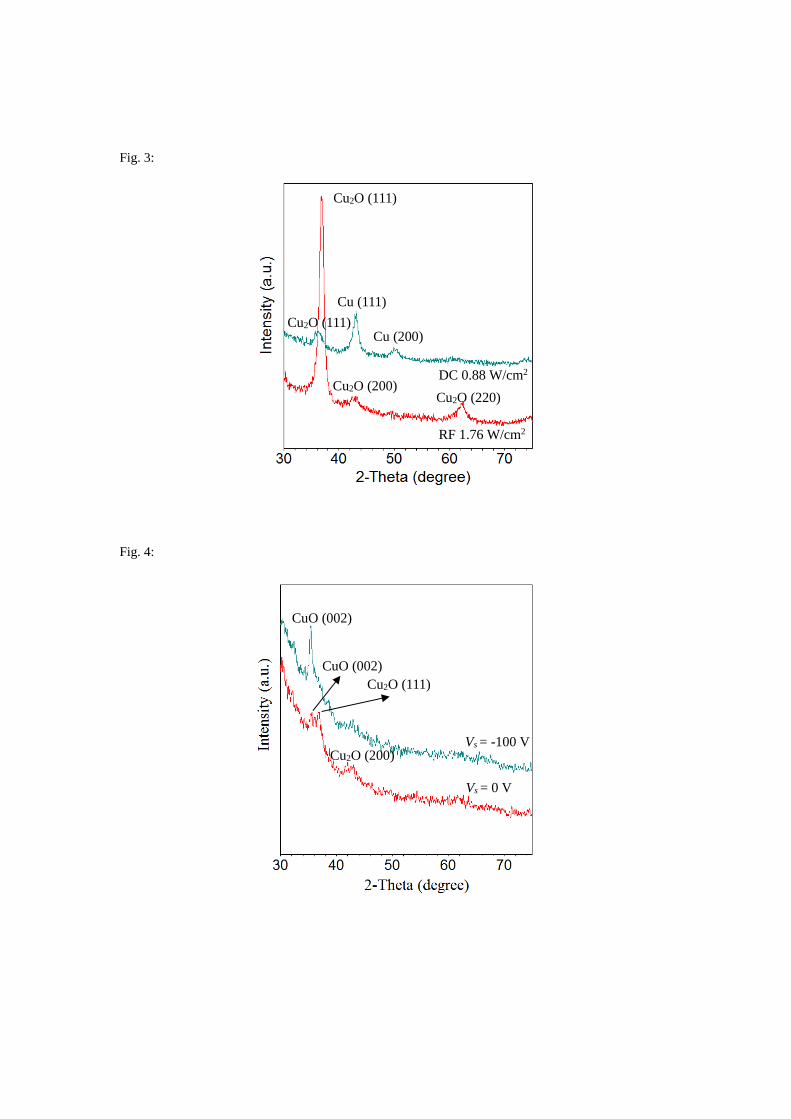
Fig 3
Fig 4
Vs = -100 V
CuO (002)
CuO (002)Cu2O (111)
Cu2O (200)
Vs = 0 V
DC 088 Wcm2
RF 176 Wcm2
Cu (111)
Cu (200)
Cu2O (111)
Cu2O (111)
Cu2O (200)Cu2O (220)
Fig 5
Fig 6
(a)
Ts = 20 degC
Ts = 400 degC
Cu (111)
Cu (200)
Cu2O
(111)
(b)
(c)

Fig 5
Fig 6
(a)
Ts = 20 degC
Ts = 400 degC
Cu (111)
Cu (200)
Cu2O
(111)
(b)
(c)
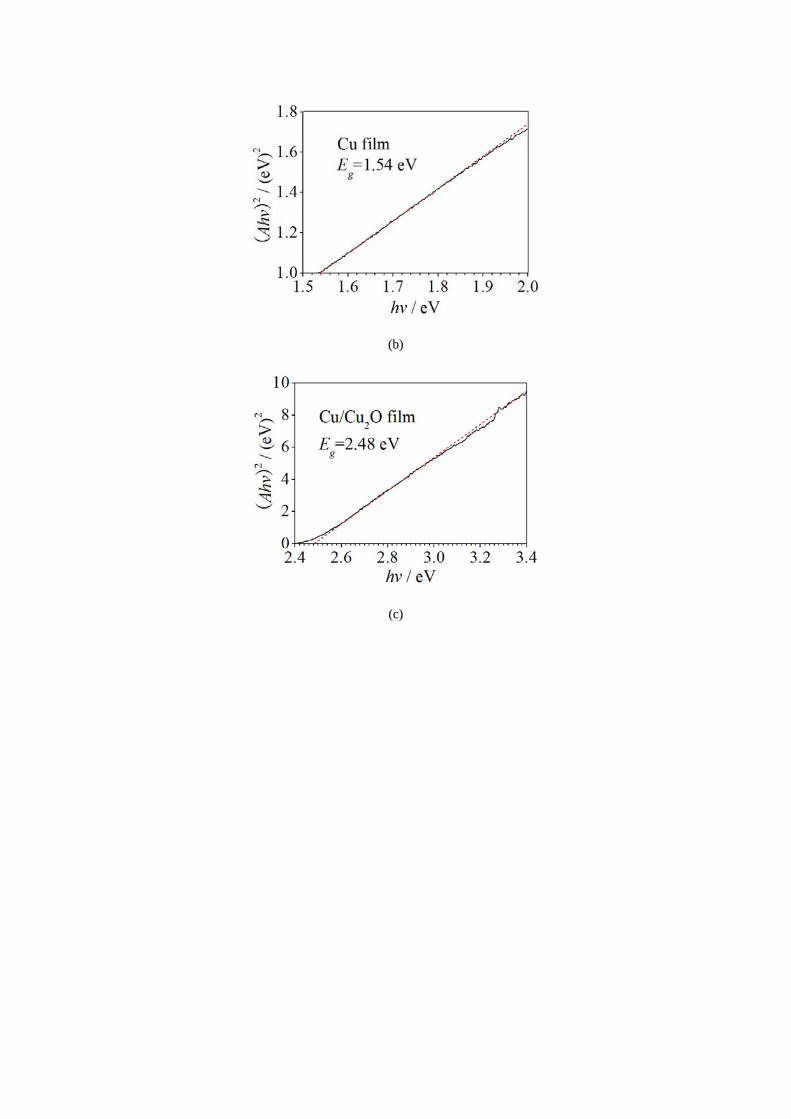
(b)
(c)