Embed Size (px)
Citation preview
1FEATURES
APPLICATIONS
DESCRIPTION
ACAdapter
VDC
GND1F m
1
2 7
5
4
6
8
bq24316DSG
bq24080Charger IC
SYSTEM
IN OUT
VBAT
FAULT
CE
VSS
ILIM
1F m
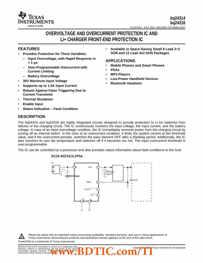
APPLICATION SCHEMATIC
bq24314bq24316
SLUS763C–JULY 2007–REVISED OCTOBER 2007www.ti.com
OVERVOLTAGE AND OVERCURRENT PROTECTION IC ANDLi+ CHARGER FRONT-END PROTECTION IC
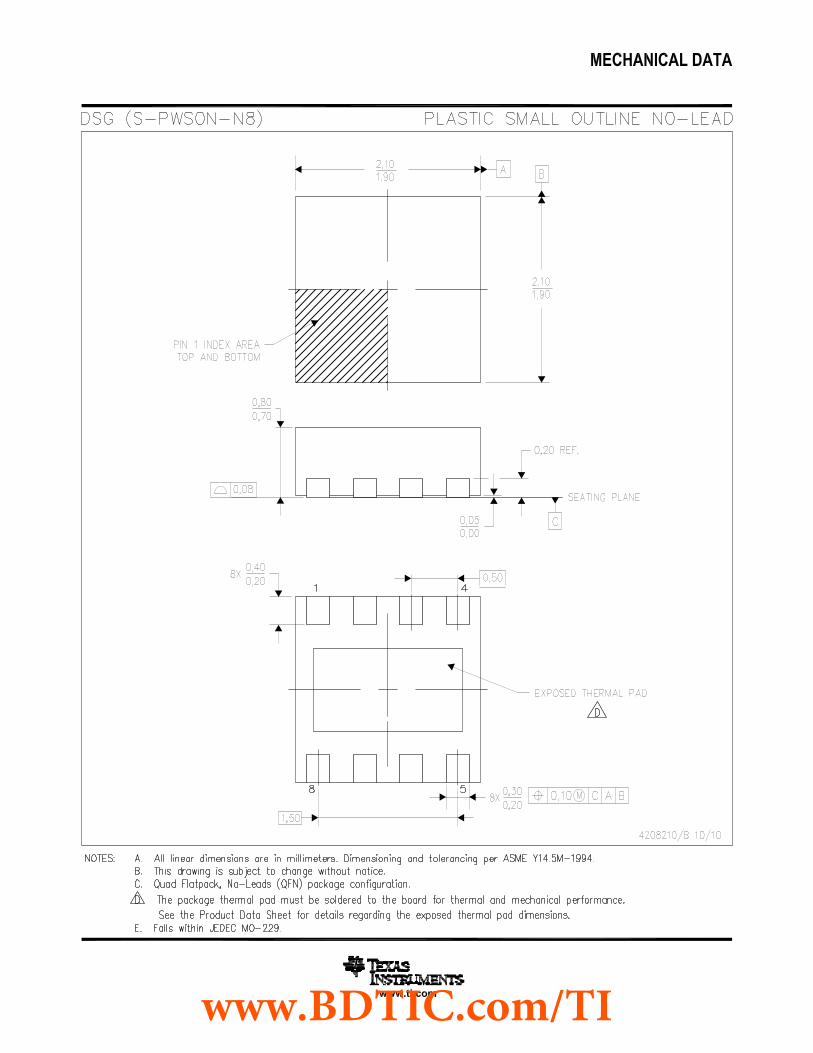
• Available in Space-Saving Small 8 Lead 2×2SON and 12 Lead 4x3 SON Packages
2• Provides Protection for Three Variables:– Input Overvoltage, with Rapid Response in
< 1 μs• Mobile Phones and Smart Phones– User-Programmable Overcurrent with• PDAsCurrent Limiting• MP3 Players– Battery Overvoltage• Low-Power Handheld Devices• 30V Maximum Input Voltage• Bluetooth Headsets
• Supports up to 1.5A Input Current• Robust Against False Triggering Due to
Current Transients• Thermal Shutdown• Enable Input• Status Indication – Fault Condition
The bq24314 and bq24316 are highly integrated circuits designed to provide protection to Li-ion batteries fromfailures of the charging circuit. The IC continuously monitors the input voltage, the input current, and the batteryvoltage. In case of an input overvoltage condition, the IC immediately removes power from the charging circuit byturning off an internal switch. In the case of an overcurrent condition, it limits the system current at the thresholdvalue, and if the overcurrent persists, switches the pass element OFF after a blanking period. Additionally, the ICalso monitors its own die temperature and switches off if it becomes too hot. The input overcurrent threshold isuser-programmable.
The IC can be controlled by a processor and also provides status information about fault conditions to the host.
1
Please be aware that an important notice concerning availability, standard warranty, and use in critical applications ofTexas Instruments semiconductor products and disclaimers thereto appears at the end of this data sheet.
2PowerPAD is a trademark of Texas Instruments.
PRODUCTION DATA information is current as of publication date. Copyright © 2007, Texas Instruments IncorporatedProducts conform to specifications per the terms of the TexasInstruments standard warranty. Production processing does notnecessarily include testing of all parameters.www.BDTIC.com/TI
www.ti.com
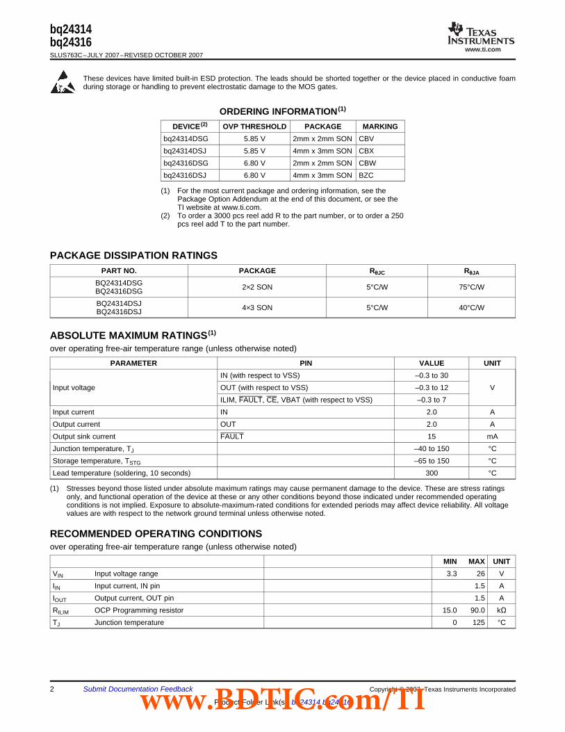
PACKAGE DISSIPATION RATINGS
ABSOLUTE MAXIMUM RATINGS (1)
RECOMMENDED OPERATING CONDITIONS
bq24314bq24316SLUS763C–JULY 2007–REVISED OCTOBER 2007
These devices have limited built-in ESD protection. The leads should be shorted together or the device placed in conductive foamduring storage or handling to prevent electrostatic damage to the MOS gates.
ORDERING INFORMATION (1)
DEVICE (2) OVP THRESHOLD PACKAGE MARKINGbq24314DSG 5.85 V 2mm x 2mm SON CBVbq24314DSJ 5.85 V 4mm x 3mm SON CBXbq24316DSG 6.80 V 2mm x 2mm SON CBWbq24316DSJ 6.80 V 4mm x 3mm SON BZC
(1) For the most current package and ordering information, see thePackage Option Addendum at the end of this document, or see theTI website at www.ti.com.
(2) To order a 3000 pcs reel add R to the part number, or to order a 250pcs reel add T to the part number.
PART NO. PACKAGE RθJC RθJA
BQ24314DSG 2×2 SON 5°C/W 75°C/WBQ24316DSGBQ24314DSJ 4×3 SON 5°C/W 40°C/WBQ24316DSJ
over operating free-air temperature range (unless otherwise noted)
PARAMETER PIN VALUE UNITIN (with respect to VSS) –0.3 to 30
Input voltage OUT (with respect to VSS) –0.3 to 12 VILIM, FAULT, CE, VBAT (with respect to VSS) –0.3 to 7
Input current IN 2.0 AOutput current OUT 2.0 AOutput sink current FAULT 15 mAJunction temperature, TJ –40 to 150 °CStorage temperature, TSTG –65 to 150 °CLead temperature (soldering, 10 seconds) 300 °C
(1) Stresses beyond those listed under absolute maximum ratings may cause permanent damage to the device. These are stress ratingsonly, and functional operation of the device at these or any other conditions beyond those indicated under recommended operatingconditions is not implied. Exposure to absolute-maximum-rated conditions for extended periods may affect device reliability. All voltagevalues are with respect to the network ground terminal unless otherwise noted.
over operating free-air temperature range (unless otherwise noted)
MIN MAX UNITVIN Input voltage range 3.3 26 VIIN Input current, IN pin 1.5 AIOUT Output current, OUT pin 1.5 ARILIM OCP Programming resistor 15.0 90.0 kΩTJ Junction temperature 0 125 °C
2 Submit Documentation Feedback Copyright © 2007, Texas Instruments Incorporated
Product Folder Link(s): bq24314 bq24316www.BDTIC.com/TI
www.ti.com
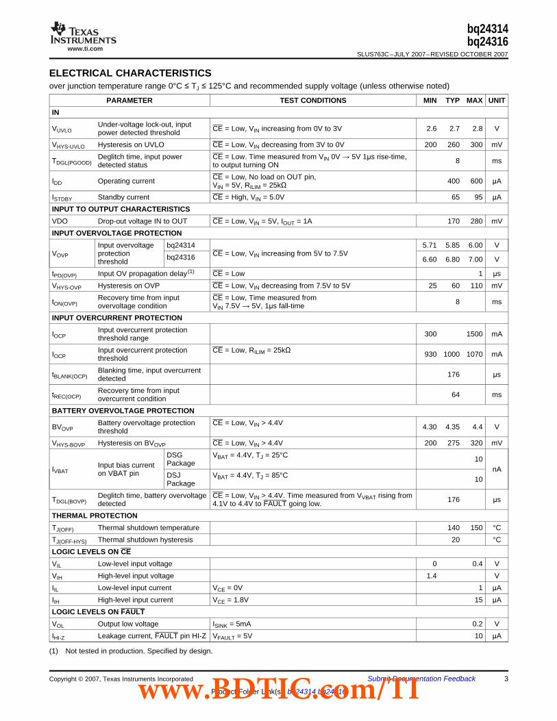
ELECTRICAL CHARACTERISTICS
bq24314bq24316
SLUS763C–JULY 2007–REVISED OCTOBER 2007
over junction temperature range 0°C ≤ TJ ≤ 125°C and recommended supply voltage (unless otherwise noted)
PARAMETER TEST CONDITIONS MIN TYP MAX UNITIN
Under-voltage lock-out, inputVUVLO CE = Low, VIN increasing from 0V to 3V 2.6 2.7 2.8 Vpower detected thresholdVHYS-UVLO Hysteresis on UVLO CE = Low, VIN decreasing from 3V to 0V 200 260 300 mV
Deglitch time, input power CE = Low. Time measured from VIN 0V → 5V 1μs rise-time,TDGL(PGOOD) 8 msdetected status to output turning ONCE = Low, No load on OUT pin,IDD Operating current 400 600 μAVIN = 5V, RILIM = 25kΩ
ISTDBY Standby current CE = High, VIN = 5.0V 65 95 μAINPUT TO OUTPUT CHARACTERISTICSVDO Drop-out voltage IN to OUT CE = Low, VIN = 5V, IOUT = 1A 170 280 mVINPUT OVERVOLTAGE PROTECTION
Input overvoltage bq24314 5.71 5.85 6.00 VVOVP protection CE = Low, VIN increasing from 5V to 7.5Vbq24316 6.60 6.80 7.00 VthresholdtPD(OVP) Input OV propagation delay (1) CE = Low 1 μsVHYS-OVP Hysteresis on OVP CE = Low, VIN decreasing from 7.5V to 5V 25 60 110 mV
Recovery time from input CE = Low, Time measured fromtON(OVP) 8 msovervoltage condition VIN 7.5V → 5V, 1μs fall-timeINPUT OVERCURRENT PROTECTION
Input overcurrent protectionIOCP 300 1500 mAthreshold rangeInput overcurrent protection CE = Low, RILIM = 25kΩIOCP 930 1000 1070 mAthresholdBlanking time, input overcurrenttBLANK(OCP) 176 μsdetectedRecovery time from inputtREC(OCP) 64 msovercurrent condition
BATTERY OVERVOLTAGE PROTECTIONBattery overvoltage protection CE = Low, VIN > 4.4VBVOVP 4.30 4.35 4.4 Vthreshold
VHYS-BOVP Hysteresis on BVOVP CE = Low, VIN > 4.4V 200 275 320 mVDSG VBAT = 4.4V, TJ = 25°C 10PackageInput bias currentIVBAT nAon VBAT pin DSJ VBAT = 4.4V, TJ = 85°C 10Package
Deglitch time, battery overvoltage CE = Low, VIN > 4.4V. Time measured from VVBAT rising fromTDGL(BOVP) 176 μsdetected 4.1V to 4.4V to FAULT going low.THERMAL PROTECTIONTJ(OFF) Thermal shutdown temperature 140 150 °CTJ(OFF-HYS) Thermal shutdown hysteresis 20 °CLOGIC LEVELS ON CEVIL Low-level input voltage 0 0.4 VVIH High-level input voltage 1.4 VIIL Low-level input current VCE = 0V 1 μAIIH High-level input current VCE = 1.8V 15 μALOGIC LEVELS ON FAULTVOL Output low voltage ISINK = 5mA 0.2 VIHI-Z Leakage current, FAULT pin HI-Z VFAULT = 5V 10 μA
(1) Not tested in production. Specified by design.
Copyright © 2007, Texas Instruments Incorporated Submit Documentation Feedback 3
Product Folder Link(s): bq24314 bq24316www.BDTIC.com/TI
www.ti.com
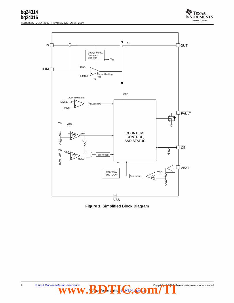
OUT
FAULT
VSS
THERMAL
SHUTDOW
CE
COUNTERS,CONTROL,
AND STATUS
ILIM
VBAT
VIN
ILIMREF
ILIMREF- Δt BLANK(OCP)
t DGL(PGOOD)
ISNS
ISNS
OFF
t DGL(BOVP)
Charge Pump,Bandgap,Bias Gen
Q1
VBG
VBG
VINVBG
OVP
UVLO
VBG
Current limitingloop
OCP comparator
IN
bq24314bq24316SLUS763C–JULY 2007–REVISED OCTOBER 2007
Figure 1. Simplified Block Diagram
4 Submit Documentation Feedback Copyright © 2007, Texas Instruments Incorporated
Product Folder Link(s): bq24314 bq24316www.BDTIC.com/TI
www.ti.com
TERMINAL FUNCTIONS
NC
VSS
FAULT
IN OUT
CE
1
2
3 6
8
7
4 5
VBAT
ILIM
bq24314DSGbq24316DSG
FAULT
NC
VSS
CE
3
4
5 8
10
9
6 7
VBAT
ILIM
2
IN 1 NC12
OUT11
bq24314DSJbq24316DSJ
IN
NC
OUT
bq24314bq24316
SLUS763C–JULY 2007–REVISED OCTOBER 2007
TERMINALI/O DESCRIPTION
NAME DSJ DSG1, 2 1 I Input power, connect to external DC supply. Connect external 1μF ceramic capacitor (minimum) to
IN VSS. For the 12 pin (DSJ-suffix) device, ensure that pins 1 and 2 are connected together on thePCB at the device.
OUT 10, 11 8 O Output terminal to the charging system. Connect external 1μF ceramic capacitor (minimum) to VSS.VBAT 8 6 I Battery voltage sense input. Connect to pack positive terminal through a resistor.
9 7 I/O Input overcurrent threshold programming. Connect a resistor to VSS to set the overcurrentILIM threshold.CE 7 5 I Chip enable input. Active low. When CE = High, the input FET is off. Internally pulled down.
Open-drain output, device status. FAULT = Low indicates that the input FET Q1 has been turned offFAULT 4 4 O due to input overvoltage, input overcurrent, battery overvoltage, or thermal shutdown.VSS 3 2 – Ground terminal
These pins may have internal circuits used for test purposes. Do not make any external connectionsNC 5, 6, 12 3 at these pins for normal operation.There is an internal electrical connection between the exposed thermal pad and the VSS pin of the
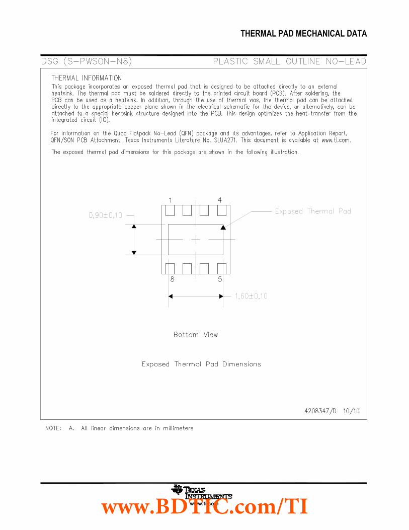
Thermal device. The thermal pad must be connected to the same potential as the VSS pin on the printed–PAD circuit board. Do not use the thermal pad as the primary ground input for the device. The VSS pinmust be connected to ground at all times.
Copyright © 2007, Texas Instruments Incorporated Submit Documentation Feedback 5
Product Folder Link(s): bq24314 bq24316www.BDTIC.com/TI
www.ti.com
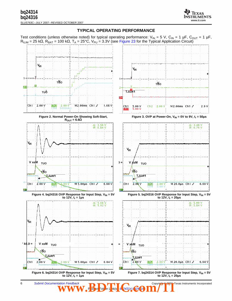
TYPICAL OPERATING PERFORMANCE
VIN
VOUT
IOUT
VIN
VOUT
FAULT
VIN
VOUT
FAULT
Max V= 6.84 V OUT
VIN
VOUT
Max V= 6.76 V OUT
FAULT
VIN
VOUT
Max V= 6.84 V OUT
FAULT
VIN
VOUT
Max V= 6.76 V OUT
FAULT
bq24314bq24316SLUS763C–JULY 2007–REVISED OCTOBER 2007
Test conditions (unless otherwise noted) for typical operating performance: VIN = 5 V, CIN = 1 μF, COUT = 1 μF,RILIM = 25 kΩ, RBAT = 100 kΩ, TA = 25°C, VPU = 3.3V (see Figure 23 for the Typical Application Circuit)
Figure 2. Normal Power-On Showing Soft-Start, Figure 3. OVP at Power-On, VIN = 0V to 9V, tr = 50μsROUT = 6.6Ω
Figure 4. bq24316 OVP Response for Input Step, VIN = 5V Figure 5. bq24316 OVP Response for Input Step, VIN = 5Vto 12V, tr = 1μs to 12V, tr = 20μs
Figure 6. bq24314 OVP Response for Input Step, VIN = 5V Figure 7. bq24314 OVP Response for Input Step, VIN = 5Vto 12V, tr = 1μs to 12V, tr = 20μs
6 Submit Documentation Feedback Copyright © 2007, Texas Instruments Incorporated
Product Folder Link(s): bq24314 bq24316www.BDTIC.com/TI
www.ti.com
VIN
VOUT
IOUT
FAULT
VIN
VOUT
IOUT
FAULT
VIN
VOUT
IOUT
FAULT
VIN
VOUT
IOUT
FAULT
VOUT
VVBAT
FAULT
VVBAT
VOUT
FAULT
Beginsoft-stop
t
= 220 s
DGL(BAT-OVP)
m
bq24314bq24316
SLUS763C–JULY 2007–REVISED OCTOBER 2007
TYPICAL OPERATING PERFORMANCE (continued)
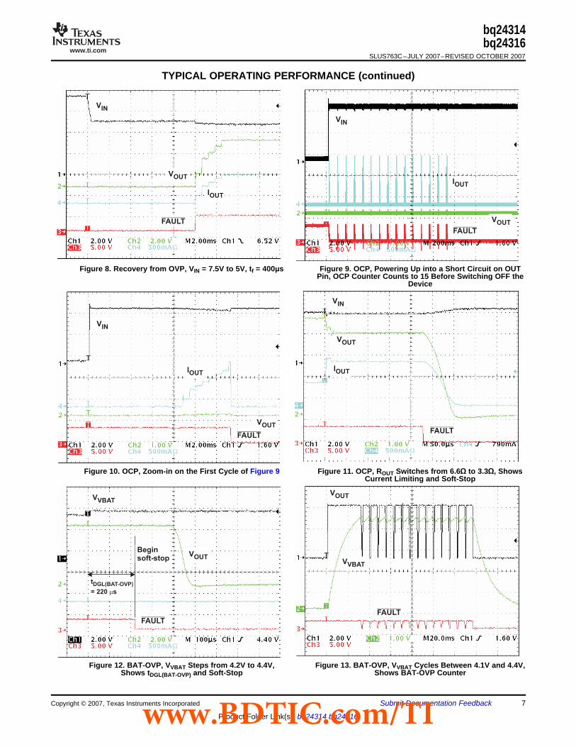
Figure 8. Recovery from OVP, VIN = 7.5V to 5V, tf = 400μs Figure 9. OCP, Powering Up into a Short Circuit on OUTPin, OCP Counter Counts to 15 Before Switching OFF the
Device
Figure 10. OCP, Zoom-in on the First Cycle of Figure 9 Figure 11. OCP, ROUT Switches from 6.6Ω to 3.3Ω, ShowsCurrent Limiting and Soft-Stop
Figure 12. BAT-OVP, VVBAT Steps from 4.2V to 4.4V, Figure 13. BAT-OVP, VVBAT Cycles Between 4.1V and 4.4V,Shows tDGL(BAT-OVP) and Soft-Stop Shows BAT-OVP Counter
Copyright © 2007, Texas Instruments Incorporated Submit Documentation Feedback 7
Product Folder Link(s): bq24314 bq24316www.BDTIC.com/TI
www.ti.com
2.4
2.45
2.5
2.55
2.6
2.65
2.7
2.75
-50 -30 -10 10 30 50 70 90 110 130
V IncreasingIN
V DecreasingIN
Temperature - C°
V, V
- V
UV
LO
HY
S-U
VL
O
100
120
140
160
180
200
220
240
260
280
0 50 100 150
V = 4 VIN
VD
O@
1A
- m
V
Temperature - C°
V = 5 VIN
6.7
6.72
6.74
6.76
6.78
6.8
6.82
-50 -30 -10 10 30 50 70 90 110 130
V IncreasingIN
V DecreasingIN
V, V
- V
OV
PH
YS
-OV
P
Temperature - C°
5.78
5.8
5.82
5.84
5.86
5.88
-50 -30 -10 10 30 50 70 90 110 130
V IncreasingIN
V DecreasingIN
Temperature - C°
V,
V-
VO
VP
HY
S-O
VP
0
200
400
600
800
1000
1200
1400
1600
0 10 20 30 40 50 60 70 80 90 100
I-
mA
OC
P
R - kILIM W
975
976
977
978
979
980
981
982
983
984
985
-50 -30 -10 10 30 50 70 90 110 130
I-
mA
OC
P
Temperature - C°
bq24314bq24316SLUS763C–JULY 2007–REVISED OCTOBER 2007
TYPICAL OPERATING PERFORMANCE (continued)
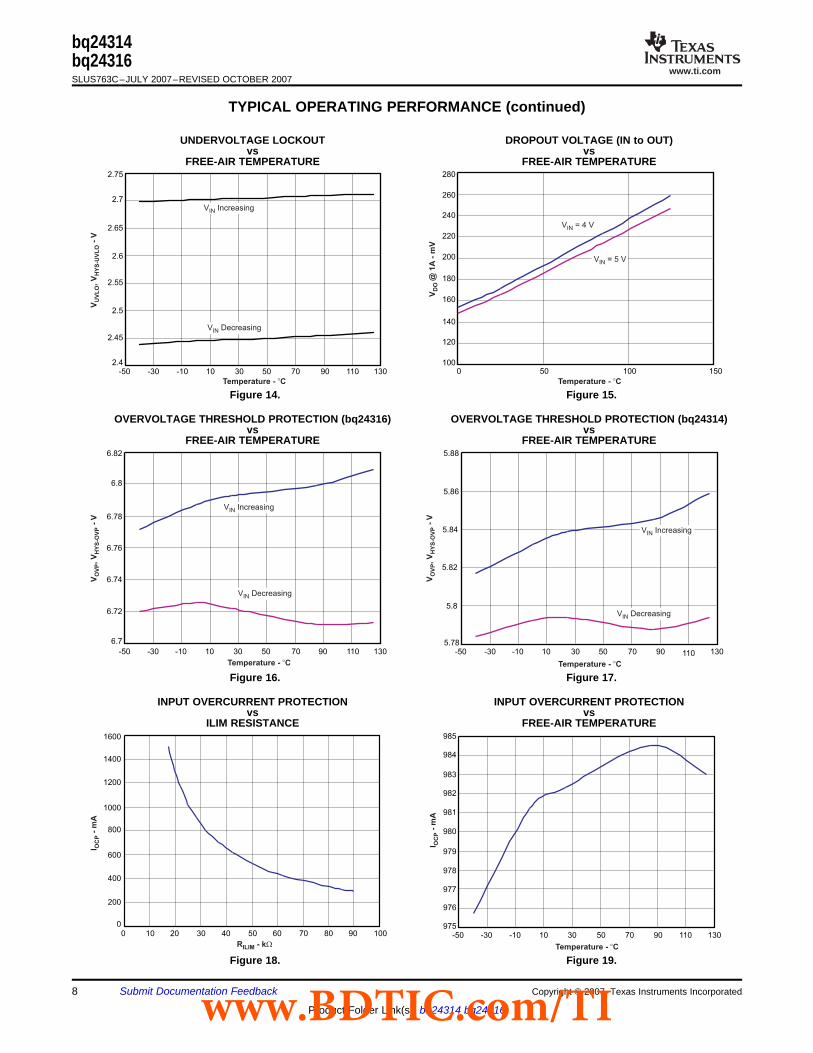
UNDERVOLTAGE LOCKOUT DROPOUT VOLTAGE (IN to OUT)vs vs
FREE-AIR TEMPERATURE FREE-AIR TEMPERATURE
Figure 14. Figure 15.
OVERVOLTAGE THRESHOLD PROTECTION (bq24316) OVERVOLTAGE THRESHOLD PROTECTION (bq24314)vs vs
FREE-AIR TEMPERATURE FREE-AIR TEMPERATURE
Figure 16. Figure 17.
INPUT OVERCURRENT PROTECTION INPUT OVERCURRENT PROTECTIONvs vs
ILIM RESISTANCE FREE-AIR TEMPERATURE
Figure 18. Figure 19.
8 Submit Documentation Feedback Copyright © 2007, Texas Instruments Incorporated
Product Folder Link(s): bq24314 bq24316www.BDTIC.com/TI
www.ti.com
4.05
4.1
4.15
4.2
4.25
4.3
4.35
4.4
-50 -30 -10 10 30 50 70 90 110 130
BV (V Increasing)OVP VBAT
Bat-OVP Recovery (V Decreasing)VBAT
BV
- V
OV
P
Temperature - C°
0
0.5
1
1.5
2
2.5
-50 -30 -10 10 30 50 70 90 110 130
Temperature - C°
I-
nA
VB
AT
0
100
200
300
400
500
600
700
800
900
0 5 10 15 20 25 30 35
I ( = Low)DD CE
I ( = High)STDBY CE
I, I
-A
DD
ST
DB
Ym
V - VIN
bq24314bq24316
SLUS763C–JULY 2007–REVISED OCTOBER 2007
TYPICAL OPERATING PERFORMANCE (continued)
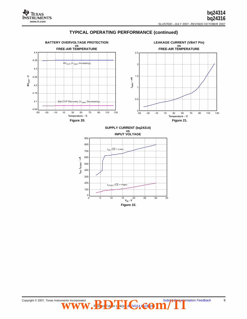
BATTERY OVERVOLTAGE PROTECTION LEAKAGE CURRENT (VBAT Pin)vs vs
FREE-AIR TEMPERATURE FREE-AIR TEMPERATURE
Figure 20. Figure 21.
SUPPLY CURRENT (bq24314)vs
INPUT VOLTAGE
Figure 22.
Copyright © 2007, Texas Instruments Incorporated Submit Documentation Feedback 9
Product Folder Link(s): bq24314 bq24316www.BDTIC.com/TI
www.ti.com
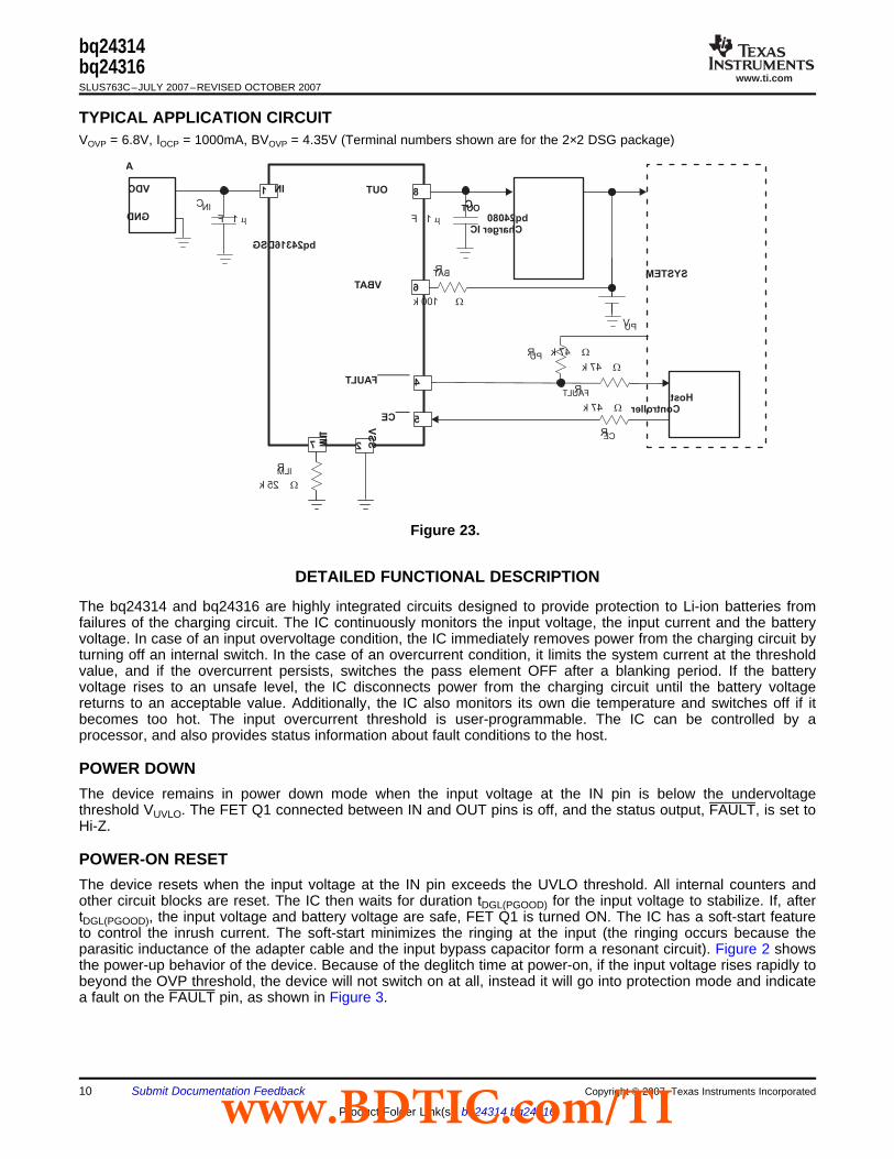
TYPICAL APPLICATION CIRCUIT
ACAdapter
VDC
GND
CIN
1
7 2
5
4
6
8
bq24316DSG
bq24080Charger IC
SYSTEM
IN OUT
VBAT
FAULT
CE
VSS
ILIM
COUTCOUT
RBAT
RCE
HostController
RFAULT
VPU
RPU
1F m1F m
100 k W
47 k W
47 k W
47 k W
RILM
25 k W
DETAILED FUNCTIONAL DESCRIPTION
POWER DOWN
POWER-ON RESET
bq24314bq24316SLUS763C–JULY 2007–REVISED OCTOBER 2007
VOVP = 6.8V, IOCP = 1000mA, BVOVP = 4.35V (Terminal numbers shown are for the 2×2 DSG package)
Figure 23.
The bq24314 and bq24316 are highly integrated circuits designed to provide protection to Li-ion batteries fromfailures of the charging circuit. The IC continuously monitors the input voltage, the input current and the batteryvoltage. In case of an input overvoltage condition, the IC immediately removes power from the charging circuit byturning off an internal switch. In the case of an overcurrent condition, it limits the system current at the thresholdvalue, and if the overcurrent persists, switches the pass element OFF after a blanking period. If the batteryvoltage rises to an unsafe level, the IC disconnects power from the charging circuit until the battery voltagereturns to an acceptable value. Additionally, the IC also monitors its own die temperature and switches off if itbecomes too hot. The input overcurrent threshold is user-programmable. The IC can be controlled by aprocessor, and also provides status information about fault conditions to the host.
The device remains in power down mode when the input voltage at the IN pin is below the undervoltagethreshold VUVLO. The FET Q1 connected between IN and OUT pins is off, and the status output, FAULT, is set toHi-Z.
The device resets when the input voltage at the IN pin exceeds the UVLO threshold. All internal counters andother circuit blocks are reset. The IC then waits for duration tDGL(PGOOD) for the input voltage to stabilize. If, aftertDGL(PGOOD), the input voltage and battery voltage are safe, FET Q1 is turned ON. The IC has a soft-start featureto control the inrush current. The soft-start minimizes the ringing at the input (the ringing occurs because theparasitic inductance of the adapter cable and the input bypass capacitor form a resonant circuit). Figure 2 showsthe power-up behavior of the device. Because of the deglitch time at power-on, if the input voltage rises rapidly tobeyond the OVP threshold, the device will not switch on at all, instead it will go into protection mode and indicatea fault on the FAULT pin, as shown in Figure 3.
10 Submit Documentation Feedback Copyright © 2007, Texas Instruments Incorporated
Product Folder Link(s): bq24314 bq24316www.BDTIC.com/TI
www.ti.com
OPERATION
Input Overvoltage Protection
Input Overcurrent Protection
Battery Overvoltage Protection
Thermal Protection
Enable Function
Fault Indication
bq24314bq24316
SLUS763C–JULY 2007–REVISED OCTOBER 2007
The device continuously monitors the input voltage, the input current, and the battery voltage as described indetail in the following sections.
If the input voltage rises above VOVP, the internal FET Q1 is turned off, removing power from the circuit. Asshown in Figure 4 to Figure 7, the response is very rapid, with the FET turning off in less than a microsecond.The FAULT pin is driven low. When the input voltage returns below VOVP – VHYS-OVP (but is still above VUVLO), theFET Q1 is turned on again after a deglitch time of tON(OVP) to ensure that the input supply has stabilized. Figure 8shows the recovery from input OVP.
The overcurrent threshold is programmed by a resistor RILIM connected from the ILIM pin to VSS. Figure 18shows the OCP threshold as a function of RILIM, and may be approximated by the following equation:IOCP = 25 ÷ RILIM (current in A, resistance in kΩ)
If the load current tries to exceed the IOCP threshold, the device limits the current for a blanking duration oftBLANK(OCP). If the load current returns to less than IOCP before tBLANK(OCP) times out, the device continues tooperate. However, if the overcurrent situation persists for tBLANK(OCP), the FET Q1 is turned off for a duration oftREC(OCP), and the FAULT pin is driven low. The FET is then turned on again after tREC(OCP) and the current ismonitored all over again. Each time an OCP fault occurs, an internal counter is incremented. If 15 OCP faultsoccur in one charge cycle, the FET is turned off permanently. The counter is cleared either by removing andre-applying input power, or by disabling and re-enabling the device with the CE pin. Figure 9 to Figure 11 showwhat happens in an overcurrent fault.
To prevent the input voltage from spiking up due to the inductance of the input cable, Q1 is turned off slowly,resulting in a “soft-stop”, as shown in Figure 11.
The battery overvoltage threshold BVOVP is internally set to 4.35V. If the battery voltage exceeds the BVOVPthreshold, the FET Q1 is turned off, and the FAULT pin is driven low. The FET is turned back on once the batteryvoltage drops to BVOVP – VHYS-BOVP (see Figure 12 and Figure 13). Each time a battery overvoltage fault occurs,an internal counter is incremented. If 15 such faults occur in one charge cycle, the FET is turned off permanently.The counter is cleared either by removing and re-applying input power, or by disabling and re-enabling thedevice with the CE pin. In the case of a battery overvoltage fault, Q1 is switched OFF gradually (see Figure 12).
If the junction temperature of the device exceeds TJ(OFF), the FET Q1 is turned off, and the FAULT pin is drivenlow. The FET is turned back on when the junction temperature falls below TJ(OFF) – TJ(OFF-HYS).
The IC has an enable pin which can be used to enable or disable the device. When the CE pin is driven high, theinternal FET is turned off. When the CE pin is low, the FET is turned on if other conditions are safe. The OCPcounter and the Bat-OVP counter are both reset when the device is disabled and re-enabled. The CE pin has aninternal pulldown resistor and can be left floating. Note that the FAULT pin functionality is also disabled when theCE pin is high.
The FAULT pin is an active-low open-drain output. It is in a high-impedance state when operating conditions aresafe, or when the device is disabled by setting CE high. With CE low, the FAULT pin goes low whenever any ofthese events occurs:• Input overvoltage• Input overcurrent• Battery overvoltage• IC Overtemperature
Copyright © 2007, Texas Instruments Incorporated Submit Documentation Feedback 11
Product Folder Link(s): bq24314 bq24316www.BDTIC.com/TI
www.ti.com
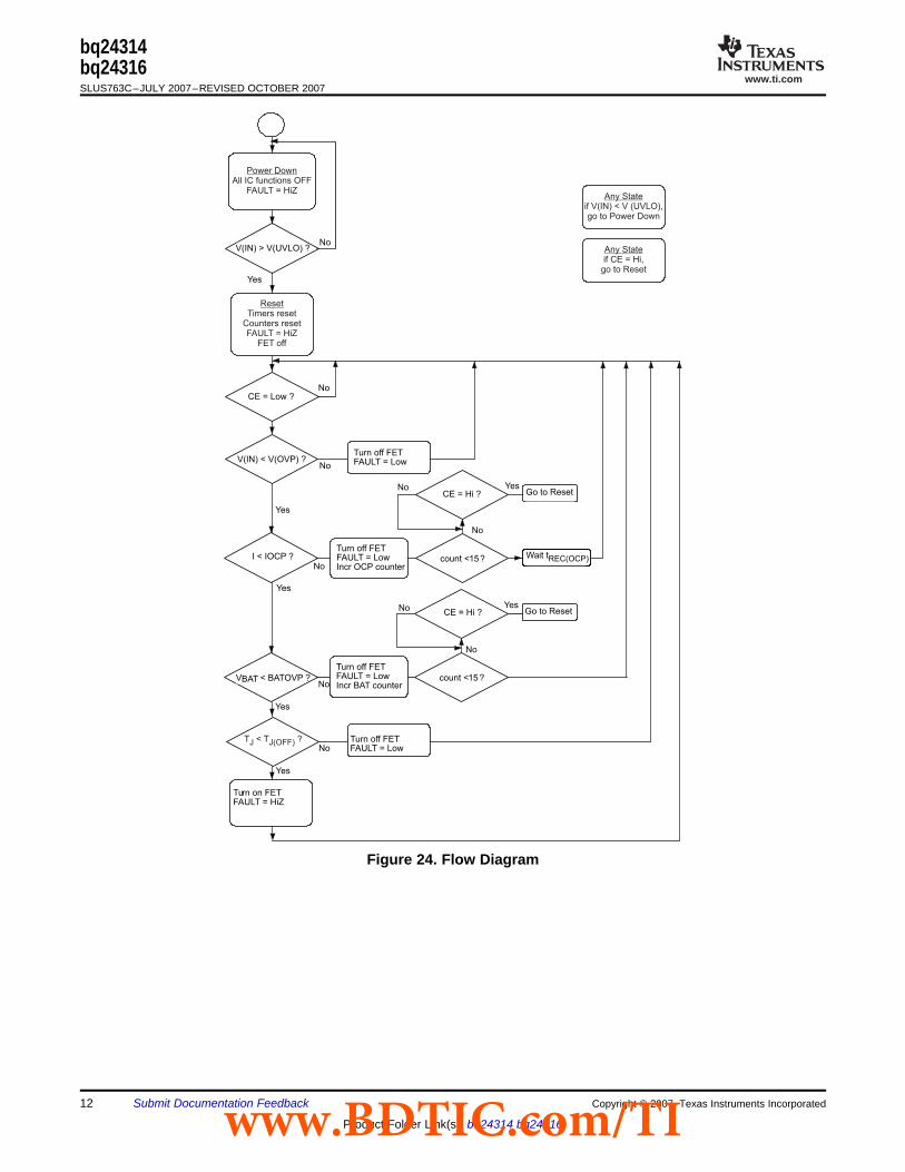
V(IN) > V(UVLO) ?No
CE = Low ?No
V(IN) < V(OVP) ?
Yes
No
Turn off FETFAULT = Low
I < IOCP ?
Yes
No
Wait tREC(OCP)
VBAT < BATOVP ?
Yes
No
Turn on FETFAULT = HiZ
Turn off FETFAULT = LowIncr OCP counter
count <15?
CE = Hi ?No
No
Go to ResetYes
Turn off FETFAULT = LowIncr BAT counter
count <15 ?
CE = Hi ? Go to ResetYes
No
No
Yes
Yes
NoTurn off FETFAULT = Low
Power DownAll IC functions OFF
FAULT = HiZ
ResetTimers reset
Counters resetFAULT = HiZ
FET off
T < T ?J J(OFF)
Any Stateif V(IN) < V (UVLO),go to Power Down
Any Stateif CE = Hi,
go to Reset
bq24314bq24316SLUS763C–JULY 2007–REVISED OCTOBER 2007
Figure 24. Flow Diagram
12 Submit Documentation Feedback Copyright © 2007, Texas Instruments Incorporated
Product Folder Link(s): bq24314 bq24316www.BDTIC.com/TI
www.ti.com
APPLICATION INFORMATION (WITH REFERENCE TO FIGURE 23)
Selection of RBAT
Selection of RCE, RFAULT, and RPU
Selection of Input and Output Bypass Capacitors
Powering Accessories
bq24314bq24316
SLUS763C–JULY 2007–REVISED OCTOBER 2007
It is strongly recommended that the battery not be tied directly to the VBAT pin of the device, as under somefailure modes of the IC, the voltage at the IN pin may appear on the VBAT pin. This voltage can be as high as30V, and applying 30V to the battery in case of the failure of the bq2431x can be hazardous. Connecting theVBAT pin through RBAT prevents a large current from flowing into the battery in case of a failure of the IC. In theinterests of safety, RBAT should have a very high value. The problem with a large RBAT is that the voltage dropacross this resistor because of the VBAT bias current IVBAT causes an error in the BVOVP threshold. This error isover and above the tolerance on the nominal 4.35V BVOVP threshold.
Choosing RBAT in the range 100kΩ to 470kΩ is a good compromise. In the case of an IC failure, with RBAT equalto 100kΩ, the maximum current flowing into the battery would be (30V – 3V) ÷ 100kΩ = 246μA, which is lowenough to be absorbed by the bias currents of the system components. RBAT equal to 100kΩ would result in aworst-case voltage drop of RBAT × IVBAT = 1mV. This is negligible to compared to the internal tolerance of 50mVon BVOVP threshold.
If the Bat-OVP function is not required, the VBAT pin should be connected to VSS.
The CE pin can be used to enable and disable the IC. If host control is not required, the CE pin can be tied toground or left un-connected, permanently enabling the device.
In applications where external control is required, the CE pin can be controlled by a host processor. As in thecase of the VBAT pin (see above), the CE pin should be connected to the host GPIO pin through as large aresistor as possible. The limitation on the resistor value is that the minimum VOH of the host GPIO pin less thedrop across the resistor should be greater than VIH of the bq2431× CE pin. The drop across the resistor is givenby RCE × IIH.
The FAULT pin is an open-drain output that goes low during OV, OC, battery-OV, and OT events. If theapplication does not require monitoring of the FAULT pin, it can be left unconnected. But if the FAULT pin has tobe monitored, it should be pulled high externally through RPU, and connected to the host through RFAULT. RFAULTprevents damage to the host controller if the bq2431x fails (see above). The resistors should be of high value, inpractice values between 22kΩ and 100kΩ should be sufficient.
The input capacitor CIN in Figure 23 is for decoupling, and serves an important purpose. Whenever there is astep change downwards in the system load current, the inductance of the input cable causes the input voltage tospike up. CIN prevents the input voltage from overshooting to dangerous levels. It is strongly recommended that aceramic capacitor of at least 1μF be used at the input of the device. It should be located in close proximity to theIN pin.
COUT in Figure 23 is also important: If a very fast (< 1μs rise time) overvoltage transient occurs at the input, thecurrent that charges COUT causes the device’s current-limiting loop to kick in, reducing the gate-drive to FET Q1.This results in improved performance for input overvoltage protection. COUT should also be a ceramic capacitor ofat least 1μF, located close to the OUT pin. COUT also serves as the input decoupling capacitor for the chargingcircuit downstream of the protection IC.
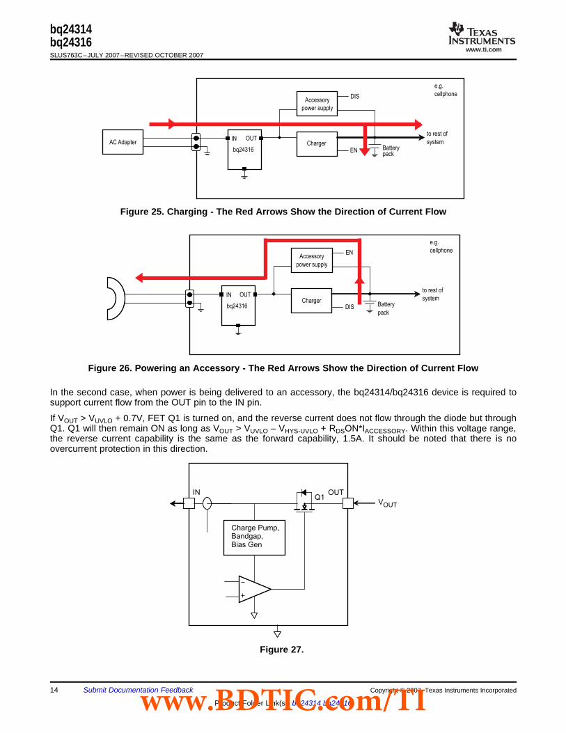
In some applications, the equipment that the protection IC resides in may be required to provide power to anaccessory (e.g. a cellphone may power a headset or an external memory card) through the same connector pinsthat are used by the adapter for charging. Figure 25 and Figure 26 illustrate typical charging andaccessory-powering scenarios:
Copyright © 2007, Texas Instruments Incorporated Submit Documentation Feedback 13
Product Folder Link(s): bq24314 bq24316www.BDTIC.com/TI
www.ti.com
bq24316
IN OUTCharger
Accessory
power supply
EN
DIS
Batterypack
to rest of
system
e.g.
cellphone
AC Adapter
bq24316
IN OUTCharger
Accessory
power supply
EN
DIS Battery
pack
to rest of
system
e.g.
cellphone
IN OUT
Charge Pump,Bandgap,Bias Gen
Q1VOUT
bq24314bq24316SLUS763C–JULY 2007–REVISED OCTOBER 2007
Figure 25. Charging - The Red Arrows Show the Direction of Current Flow
Figure 26. Powering an Accessory - The Red Arrows Show the Direction of Current Flow
In the second case, when power is being delivered to an accessory, the bq24314/bq24316 device is required tosupport current flow from the OUT pin to the IN pin.
If VOUT > VUVLO + 0.7V, FET Q1 is turned on, and the reverse current does not flow through the diode but throughQ1. Q1 will then remain ON as long as VOUT > VUVLO – VHYS-UVLO + RDSON*IACCESSORY. Within this voltage range,the reverse current capability is the same as the forward capability, 1.5A. It should be noted that there is noovercurrent protection in this direction.
Figure 27.
14 Submit Documentation Feedback Copyright © 2007, Texas Instruments Incorporated
Product Folder Link(s): bq24314 bq24316www.BDTIC.com/TI

www.ti.com
PCB Layout Guidelines:
bq24314bq24316
SLUS763C–JULY 2007–REVISED OCTOBER 2007
• This device is a protection device, and is meant to protect down-stream circuitry from hazardous voltages.Potentially, high voltages may be applied to this IC. It has to be ensured that the edge-to-edge clearances ofPCB traces satisfy the design rules for high voltages.
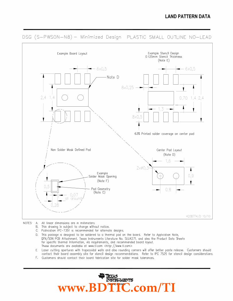
• The device uses SON packages with a PowerPAD™. For good thermal performance, the PowerPAD shouldbe thermally coupled with the PCB ground plane. In most applications, this will require a copper pad directlyunder the IC. This copper pad should be connected to the ground plane with an array of thermal vias.
• CIN and COUT should be located close to the IC. Other components like RILIM and RBAT should also be locatedclose to the IC.
Copyright © 2007, Texas Instruments Incorporated Submit Documentation Feedback 15
Product Folder Link(s): bq24314 bq24316www.BDTIC.com/TI
www.ti.com
bq24314bq24316SLUS763C–JULY 2007–REVISED OCTOBER 2007
Revision History
Changes from Revision B (September 2007) to Revision C .......................................................................................... Page
• Changed bq24314DSJ marking from preview to CBX .......................................................................................................... 2• Changed bq24316DSJ marking from preview to BZC........................................................................................................... 2
16 Submit Documentation Feedback Copyright © 2007, Texas Instruments Incorporated
Product Folder Link(s): bq24314 bq24316www.BDTIC.com/TI
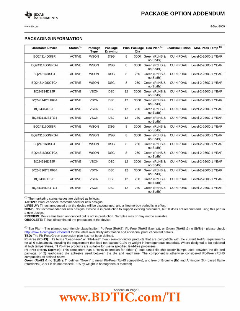
PACKAGING INFORMATION
Orderable Device Status (1) PackageType
PackageDrawing
Pins PackageQty
Eco Plan (2) Lead/Ball Finish MSL Peak Temp (3)
BQ24314DSGR ACTIVE WSON DSG 8 3000 Green (RoHS &no Sb/Br)
CU NIPDAU Level-2-260C-1 YEAR
BQ24314DSGRG4 ACTIVE WSON DSG 8 3000 Green (RoHS &no Sb/Br)
CU NIPDAU Level-2-260C-1 YEAR
BQ24314DSGT ACTIVE WSON DSG 8 250 Green (RoHS &no Sb/Br)
CU NIPDAU Level-2-260C-1 YEAR
BQ24314DSGTG4 ACTIVE WSON DSG 8 250 Green (RoHS &no Sb/Br)
CU NIPDAU Level-2-260C-1 YEAR
BQ24314DSJR ACTIVE VSON DSJ 12 3000 Green (RoHS &no Sb/Br)
CU NIPDAU Level-2-260C-1 YEAR
BQ24314DSJRG4 ACTIVE VSON DSJ 12 3000 Green (RoHS &no Sb/Br)
CU NIPDAU Level-2-260C-1 YEAR
BQ24314DSJT ACTIVE VSON DSJ 12 250 Green (RoHS &no Sb/Br)
CU NIPDAU Level-2-260C-1 YEAR
BQ24314DSJTG4 ACTIVE VSON DSJ 12 250 Green (RoHS &no Sb/Br)
CU NIPDAU Level-2-260C-1 YEAR
BQ24316DSGR ACTIVE WSON DSG 8 3000 Green (RoHS &no Sb/Br)
CU NIPDAU Level-2-260C-1 YEAR
BQ24316DSGRG4 ACTIVE WSON DSG 8 3000 Green (RoHS &no Sb/Br)
CU NIPDAU Level-2-260C-1 YEAR
BQ24316DSGT ACTIVE WSON DSG 8 250 Green (RoHS &no Sb/Br)
CU NIPDAU Level-2-260C-1 YEAR
BQ24316DSGTG4 ACTIVE WSON DSG 8 250 Green (RoHS &no Sb/Br)
CU NIPDAU Level-2-260C-1 YEAR
BQ24316DSJR ACTIVE VSON DSJ 12 3000 Green (RoHS &no Sb/Br)
CU NIPDAU Level-2-260C-1 YEAR
BQ24316DSJRG4 ACTIVE VSON DSJ 12 3000 Green (RoHS &no Sb/Br)
CU NIPDAU Level-2-260C-1 YEAR
BQ24316DSJT ACTIVE VSON DSJ 12 250 Green (RoHS &no Sb/Br)
CU NIPDAU Level-2-260C-1 YEAR
BQ24316DSJTG4 ACTIVE VSON DSJ 12 250 Green (RoHS &no Sb/Br)
CU NIPDAU Level-2-260C-1 YEAR
(1) The marketing status values are defined as follows:ACTIVE: Product device recommended for new designs.LIFEBUY: TI has announced that the device will be discontinued, and a lifetime-buy period is in effect.NRND: Not recommended for new designs. Device is in production to support existing customers, but TI does not recommend using this part ina new design.PREVIEW: Device has been announced but is not in production. Samples may or may not be available.OBSOLETE: TI has discontinued the production of the device.
(2) Eco Plan - The planned eco-friendly classification: Pb-Free (RoHS), Pb-Free (RoHS Exempt), or Green (RoHS & no Sb/Br) - please checkhttp://www.ti.com/productcontent for the latest availability information and additional product content details.TBD: The Pb-Free/Green conversion plan has not been defined.Pb-Free (RoHS): TI's terms "Lead-Free" or "Pb-Free" mean semiconductor products that are compatible with the current RoHS requirementsfor all 6 substances, including the requirement that lead not exceed 0.1% by weight in homogeneous materials. Where designed to be solderedat high temperatures, TI Pb-Free products are suitable for use in specified lead-free processes.Pb-Free (RoHS Exempt): This component has a RoHS exemption for either 1) lead-based flip-chip solder bumps used between the die andpackage, or 2) lead-based die adhesive used between the die and leadframe. The component is otherwise considered Pb-Free (RoHScompatible) as defined above.Green (RoHS & no Sb/Br): TI defines "Green" to mean Pb-Free (RoHS compatible), and free of Bromine (Br) and Antimony (Sb) based flameretardants (Br or Sb do not exceed 0.1% by weight in homogeneous material)
PACKAGE OPTION ADDENDUM
www.ti.com 8-Dec-2009
Addendum-Page 1
www.BDTIC.com/TI
(3) MSL, Peak Temp. -- The Moisture Sensitivity Level rating according to the JEDEC industry standard classifications, and peak soldertemperature.
Important Information and Disclaimer:The information provided on this page represents TI's knowledge and belief as of the date that it isprovided. TI bases its knowledge and belief on information provided by third parties, and makes no representation or warranty as to theaccuracy of such information. Efforts are underway to better integrate information from third parties. TI has taken and continues to takereasonable steps to provide representative and accurate information but may not have conducted destructive testing or chemical analysis onincoming materials and chemicals. TI and TI suppliers consider certain information to be proprietary, and thus CAS numbers and other limitedinformation may not be available for release.
In no event shall TI's liability arising out of such information exceed the total purchase price of the TI part(s) at issue in this document sold by TIto Customer on an annual basis.
PACKAGE OPTION ADDENDUM
www.ti.com 8-Dec-2009
Addendum-Page 2
www.BDTIC.com/TI
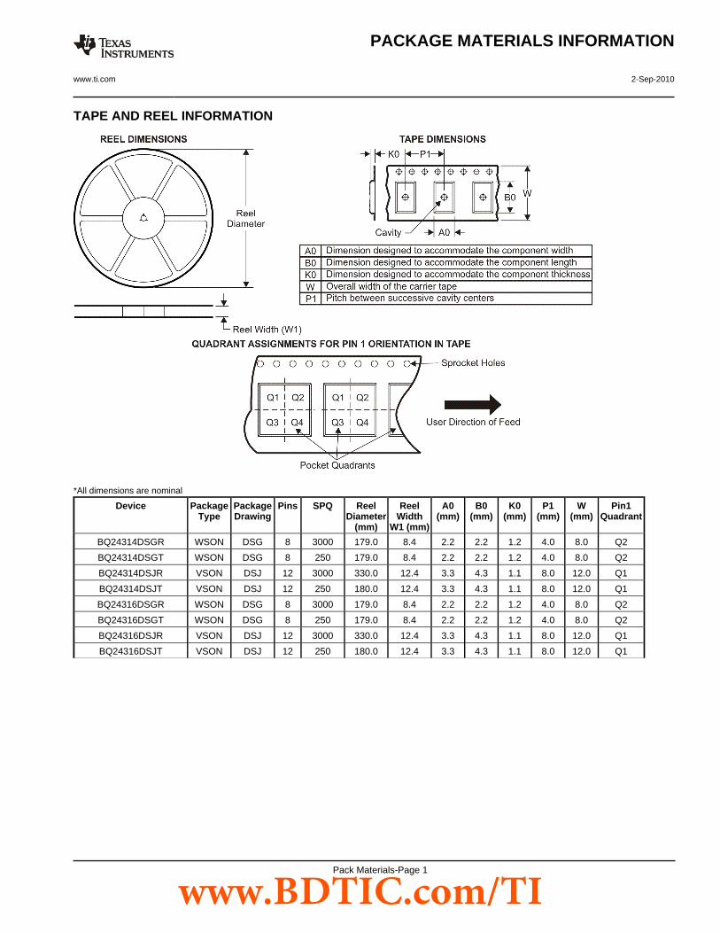
TAPE AND REEL INFORMATION
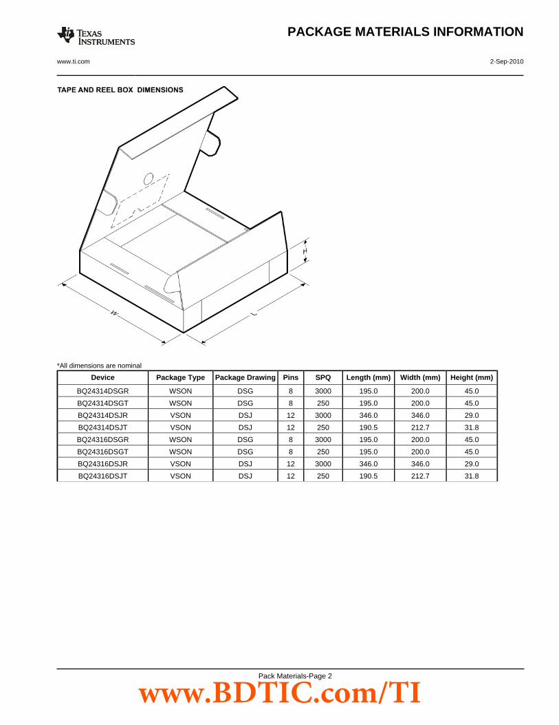
*All dimensions are nominal
Device PackageType
PackageDrawing
Pins SPQ ReelDiameter
(mm)
ReelWidth
W1 (mm)
A0(mm)
B0(mm)
K0(mm)
P1(mm)
W(mm)
Pin1Quadrant
BQ24314DSGR WSON DSG 8 3000 179.0 8.4 2.2 2.2 1.2 4.0 8.0 Q2
BQ24314DSGT WSON DSG 8 250 179.0 8.4 2.2 2.2 1.2 4.0 8.0 Q2
BQ24314DSJR VSON DSJ 12 3000 330.0 12.4 3.3 4.3 1.1 8.0 12.0 Q1
BQ24314DSJT VSON DSJ 12 250 180.0 12.4 3.3 4.3 1.1 8.0 12.0 Q1
BQ24316DSGR WSON DSG 8 3000 179.0 8.4 2.2 2.2 1.2 4.0 8.0 Q2
BQ24316DSGT WSON DSG 8 250 179.0 8.4 2.2 2.2 1.2 4.0 8.0 Q2
BQ24316DSJR VSON DSJ 12 3000 330.0 12.4 3.3 4.3 1.1 8.0 12.0 Q1
BQ24316DSJT VSON DSJ 12 250 180.0 12.4 3.3 4.3 1.1 8.0 12.0 Q1
PACKAGE MATERIALS INFORMATION
www.ti.com 2-Sep-2010
Pack Materials-Page 1
www.BDTIC.com/TI
*All dimensions are nominal
Device Package Type Package Drawing Pins SPQ Length (mm) Width (mm) Height (mm)
BQ24314DSGR WSON DSG 8 3000 195.0 200.0 45.0
BQ24314DSGT WSON DSG 8 250 195.0 200.0 45.0
BQ24314DSJR VSON DSJ 12 3000 346.0 346.0 29.0
BQ24314DSJT VSON DSJ 12 250 190.5 212.7 31.8
BQ24316DSGR WSON DSG 8 3000 195.0 200.0 45.0
BQ24316DSGT WSON DSG 8 250 195.0 200.0 45.0
BQ24316DSJR VSON DSJ 12 3000 346.0 346.0 29.0
BQ24316DSJT VSON DSJ 12 250 190.5 212.7 31.8
PACKAGE MATERIALS INFORMATION
www.ti.com 2-Sep-2010
Pack Materials-Page 2
www.BDTIC.com/TI
www.BDTIC.com/TI
www.BDTIC.com/TI
www.BDTIC.com/TI
www.BDTIC.com/TI
www.BDTIC.com/TI
IMPORTANT NOTICE
Texas Instruments Incorporated and its subsidiaries (TI) reserve the right to make corrections, modifications, enhancements, improvements,and other changes to its products and services at any time and to discontinue any product or service without notice. Customers shouldobtain the latest relevant information before placing orders and should verify that such information is current and complete. All products aresold subject to TI’s terms and conditions of sale supplied at the time of order acknowledgment.
TI warrants performance of its hardware products to the specifications applicable at the time of sale in accordance with TI’s standardwarranty. Testing and other quality control techniques are used to the extent TI deems necessary to support this warranty. Except wheremandated by government requirements, testing of all parameters of each product is not necessarily performed.
TI assumes no liability for applications assistance or customer product design. Customers are responsible for their products andapplications using TI components. To minimize the risks associated with customer products and applications, customers should provideadequate design and operating safeguards.
TI does not warrant or represent that any license, either express or implied, is granted under any TI patent right, copyright, mask work right,or other TI intellectual property right relating to any combination, machine, or process in which TI products or services are used. Informationpublished by TI regarding third-party products or services does not constitute a license from TI to use such products or services or awarranty or endorsement thereof. Use of such information may require a license from a third party under the patents or other intellectualproperty of the third party, or a license from TI under the patents or other intellectual property of TI.
Reproduction of TI information in TI data books or data sheets is permissible only if reproduction is without alteration and is accompaniedby all associated warranties, conditions, limitations, and notices. Reproduction of this information with alteration is an unfair and deceptivebusiness practice. TI is not responsible or liable for such altered documentation. Information of third parties may be subject to additionalrestrictions.
Resale of TI products or services with statements different from or beyond the parameters stated by TI for that product or service voids allexpress and any implied warranties for the associated TI product or service and is an unfair and deceptive business practice. TI is notresponsible or liable for any such statements.
TI products are not authorized for use in safety-critical applications (such as life support) where a failure of the TI product would reasonablybe expected to cause severe personal injury or death, unless officers of the parties have executed an agreement specifically governingsuch use. Buyers represent that they have all necessary expertise in the safety and regulatory ramifications of their applications, andacknowledge and agree that they are solely responsible for all legal, regulatory and safety-related requirements concerning their productsand any use of TI products in such safety-critical applications, notwithstanding any applications-related information or support that may beprovided by TI. Further, Buyers must fully indemnify TI and its representatives against any damages arising out of the use of TI products insuch safety-critical applications.
TI products are neither designed nor intended for use in military/aerospace applications or environments unless the TI products arespecifically designated by TI as military-grade or "enhanced plastic." Only products designated by TI as military-grade meet militaryspecifications. Buyers acknowledge and agree that any such use of TI products which TI has not designated as military-grade is solely atthe Buyer's risk, and that they are solely responsible for compliance with all legal and regulatory requirements in connection with such use.
TI products are neither designed nor intended for use in automotive applications or environments unless the specific TI products aredesignated by TI as compliant with ISO/TS 16949 requirements. Buyers acknowledge and agree that, if they use any non-designatedproducts in automotive applications, TI will not be responsible for any failure to meet such requirements.
Following are URLs where you can obtain information on other Texas Instruments products and application solutions:
Products Applications
Amplifiers amplifier.ti.com Audio www.ti.com/audio
Data Converters dataconverter.ti.com Automotive www.ti.com/automotive
DLP® Products www.dlp.com Communications and www.ti.com/communicationsTelecom
DSP dsp.ti.com Computers and www.ti.com/computersPeripherals
Clocks and Timers www.ti.com/clocks Consumer Electronics www.ti.com/consumer-apps
Interface interface.ti.com Energy www.ti.com/energy
Logic logic.ti.com Industrial www.ti.com/industrial
Power Mgmt power.ti.com Medical www.ti.com/medical
Microcontrollers microcontroller.ti.com Security www.ti.com/security
RFID www.ti-rfid.com Space, Avionics & www.ti.com/space-avionics-defenseDefense
RF/IF and ZigBee® Solutions www.ti.com/lprf Video and Imaging www.ti.com/video
Wireless www.ti.com/wireless-apps
Mailing Address: Texas Instruments, Post Office Box 655303, Dallas, Texas 75265Copyright © 2010, Texas Instruments Incorporated
www.BDTIC.com/TI