Embed Size (px)
Citation preview

1
Kang L. WangECE, MSE & PhysicsUniversity of California - Los Angeles (E: [email protected]; P:310-825-1609)
Overview of Magnetics and Spintronics
@ Monterey, CA March 21-23, 2017
Qinglin HeCecile Grezes
Guoqiang Yu Xiang LiPramey Upadhyaya
Alex Grutter

2
The Need: Energy efficient high performance
• Deep Learning !• Big data• Autonomous systems• Intelligent systems Watson
Deep Learning
Energy and power dissipationMemory, Memory… .
• Computing in Memory• Neuromorphics• Memory intensive systems
The progress in nonvolatile spintronics memory: Low power, High Density and Endurance, …

Information/Electronics systems Device level -Size and V scaling System level -Memory (Storage)
Data Bus
ALUCaches
MemoryRegisters
CPUSoftware Programs
Microprocessor
Storage(nonvolatile)
Von Neumann’s Limit
High endurance
fJ /switch
10~100 pJ/bit

4
Collective Spintronics
Complementary to CMOSCollective
spins
Leakage
Sub-threshold
Low dynamic powernonvolatility
Low voltage & subthreshold
Why Spintronics?
Device & Systems levelsRoom Temperature
Dynamic energy: CV2f &The limit: E=NkTln(2)= N3x10-21 Jx
FM Collective• Single crystalline not needed – no epi• Reproducible• Backend – Tprocess < 400 C
(order parameters)
𝑯𝑯 = −𝟏𝟏/𝟐𝟐𝒊𝒊,𝒋𝒋
𝑱𝑱𝒊𝒊,𝒋𝒋𝑺𝑺𝒊𝒊 ⋅ 𝑺𝑺𝒋𝒋
Heisenberg exchange
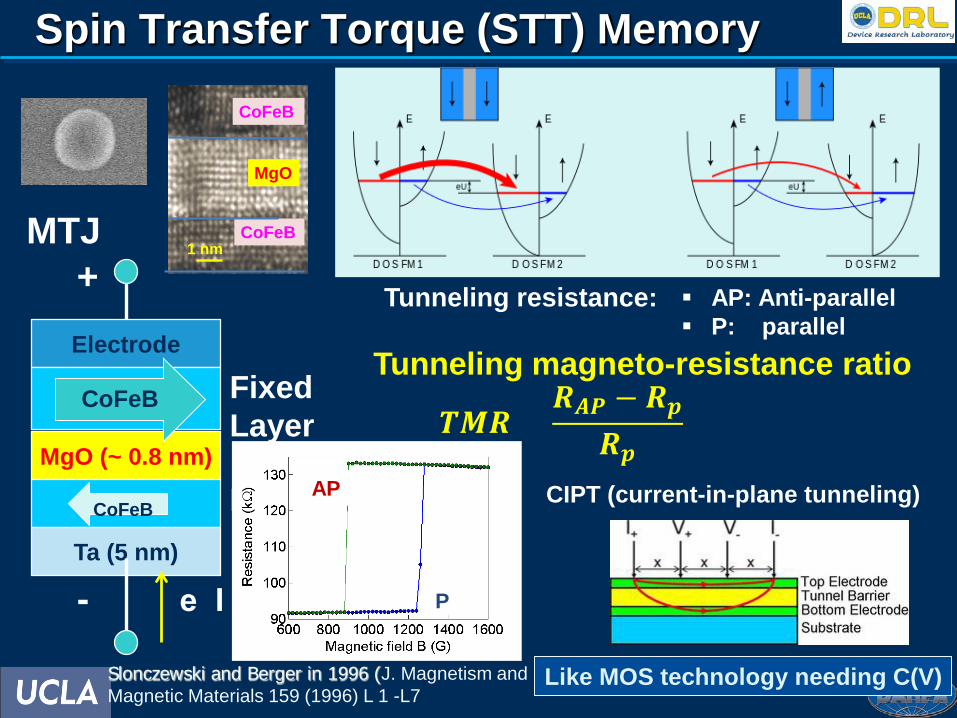
MgO (~ 0.8 nm)
CoFeB
Ta (5 nm)
+
-
Electrode
CoFeB
e I ≠ 0 , V ≠ 0
Fixed Layer
Free Layer
CoFeB
CoFeB
Tunneling resistance:
Tunneling magneto-resistance ratio
𝑻𝑻𝑻𝑻𝑻𝑻 =𝑻𝑻𝑨𝑨𝑨𝑨 − 𝑻𝑻𝒑𝒑
𝑻𝑻𝒑𝒑
Spin Transfer Torque (STT) Memory
1 nm
CoFeB
MgO
CoFeBMTJ
CIPT (current-in-plane tunneling)
AP: Anti-parallel P: parallel
P
AP
Like MOS technology needing C(V)Slonczewski and Berger in 1996 (J. Magnetism and Magnetic Materials 159 (1996) L 1 -L7

Spin Transfer Torque (STT) dynamics
MgO (~ 0.8 nm)
CoFeB
Ta (5 nm)
+
-
CoFeB
Electrode
e I ≠ 0 , V ≠ 0
Fixed Layer
Free Layer
LLG (Landau-Lifshitz-Gilbert Equation:
0≠If M and p are not colinear
Predicted by Slonczewski and Berger in 1996 (J. Magnetism and Magnetic Materials 159 (1996) L 1 -L7
Heff
Magnetization
Spin Torque
Damping
SpinPolarization
• During Current Pulse –Spin torque transferred to turn the magnet
• Speed: Precessing or FMR (acoustic)
HSTT
Precessing damping STT
𝜕𝜕𝑡𝑡𝒎𝒎 = −𝛾𝛾𝒎𝒎 × 𝑯𝑯 𝒎𝒎 + 𝛼𝛼𝒎𝒎 × 𝜕𝜕𝑡𝑡𝒎𝒎
6
𝛼𝛼(𝒎𝒎 × 𝒎𝒎 × 𝑯𝑯 )− 𝒈𝒈𝑱𝑱𝒎𝒎 × (𝒎𝒎 × 𝒑𝒑)

STT Status, Scaling and Voltage-Controlled
Current-driven:Too much power & not scalable!
Spin Transfer TorqueSTT-MRAM (2016) 1 Gb
Khalili and Wang, Spin, 2, 1240002 (2012)Wang, Alzate, and Khalili, J. Phys. D: Appl. Phys., 46, 074003 (2013)
Type Flash PCRAM FERAM RRAM STTRAMWrite Energy/ bit > 1 nJ ~ 100 pJ ~ 1 pJ ~ 1 pJ ~ 100 fJ
Speed 1 us~1 ms ~ 50 ns ~ 50 ns ~ 10 ns 0.1 – 10 nsEndurance Very Low
1000Low moderate Low~ mid Very High
1015
Density (F2) 4 – 8 6 – 10 6 – 10 6 – 10 6 – 20 Maturity Product Product Product R&D R&D
Slonczewski and Berger in 1996 (J. Magnetism and Magnetic Materials 159 (1996) L 1 -L7
< 1 nm
Everspin, Avalanches, etc.
Global, Intel, Samsung, TSMC, SMIC, Toshiba/SK Hynix, … .
CMOS at 65 nm: 1 fJ

8
Beyond STT: Riding on the success of itSpin Orbit Coupling (SOC) Engineering
SOC
Spin Hall, Rashba, Spin Orbit Torque, VCMA, Dzyaloshinskii- Morya Interaction (DMI), Skyrmionics,, Topological matters, etc… .
Low voltage & Low power
SOC ~ Z3~4
+V
→𝑩𝑩𝒍𝒍
ℋ𝑆𝑆𝑆𝑆 = −ℏ
4𝑚𝑚02𝑐𝑐2
𝝈𝝈 ⋅ 𝒑𝒑 × 𝛁𝛁𝜙𝜙
ℋ𝑻𝑻𝑹𝑹𝑹𝑹𝑹𝑹𝑹𝑹𝑹𝑹 = 𝜶𝜶𝝈𝝈 𝒑𝒑 × 𝒛𝒛• Interface of heterostructure:
• For Bulk: Spin Hall
𝑬𝑬
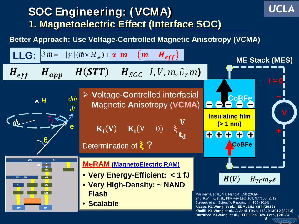
MeRAM (MagnetoElectric RAM)
• Very Energy-Efficient: < 1 fJ• Very High-Density: ~ NAND
Flash• Scalable
Maruyama et al., Nat Nano 4, 158 (2009);Zhu, KW , IK, et al., Phy Rev Lett, 108, 977203 (2012)Stewart, et al., Scientific Reports, 4, 4105 (2014)Alzate, KL Wang, et al., IEDM, 681-684 (2012)Khalili, KL Wang et al., J. Appl. Phys. 113, 013912 (2013)Dorrance, KLWang et al., IEEE Elec. Dev. Lett., (20134
Insulating film(> 1 nm)
CoBFe
CoBFe
+
−
V
I ≈ 0
+ + + + +
− − − − −
ME Stack (MES)
SOC Engineering: (VCMA)1. Magnetoelectric Effect (Interface SOC)
9
| | ( ) ( )t eff tm m H m mγ α∂ = − × + ×∂ LLG:
𝑯𝑯 𝑽𝑽 = 𝐻𝐻𝑉𝑉𝑉𝑉𝑚𝑚𝑧𝑧𝒛𝒛
𝛼𝛼(𝒎𝒎 × 𝒎𝒎 × 𝑯𝑯𝒆𝒆𝒆𝒆𝒆𝒆 )
θ
H
edτ
dmdt
𝝓𝝓
Voltage-Controlled interfacial Magnetic Anisotropy (VCMA)
𝐊𝐊𝐢𝐢 𝐕𝐕 = 𝐊𝐊𝐢𝐢 V = 0 − 𝛏𝛏𝐕𝐕𝐭𝐭𝐝𝐝
Determination of 𝛏𝛏 ?
Better Approach: Use Voltage-Controlled Magnetic Anisotropy (VCMA)
𝑯𝑯𝒆𝒆𝒆𝒆𝒆𝒆 = 𝑯𝑯𝑹𝑹𝒑𝒑𝒑𝒑 + 𝑯𝑯 𝑺𝑺𝑻𝑻𝑻𝑻 + 𝑯𝑯𝑆𝑆𝑆𝑆𝑉𝑉 (𝐼𝐼,𝑉𝑉,𝑚𝑚, ∂𝑟𝑟𝑚𝑚)

Switching Mechanism: VCMA driven precession
10
m
p
• With every properly timed pulse, the magnetization rotates 180 degrees
Voltage controlled magnetic anisotropy (VCMA) driven precessional switching
𝑯𝑯𝒆𝒆𝒆𝒆𝒆𝒆

Magnetic tunnel junction device
Perpendicular anisotropy, 50 nm junction diameter Resistance-area product = 650 Ωµm2
102 x larger than STT-MTJs Reduce the Ohmic dissipation
Perpendicular anisotropy
Electric-field modulation of perpendicular
coercivity:𝛏𝛏 =140 Oe/V (~ 30 fJ/Vm)
TMR up to 250 %
Modulation of interfacial anisotropy by applied voltage Negative (positive) voltages increase (decrease) the perpendicular coercivity
TMR ~ 165%

Esw =Vsw2
RAtsw ×
π𝐝𝐝𝟐𝟐
4
RA = 650 Ω.μm2
• Size independent write voltage and speed
• Write energy scales as ~ d2
< 1fJ/bit
Write energy <1fJ/bit for bit size < 20 nm
C. Grezes, K L Wang et al., Appl. Phys. Lett (2015)This is based on earlier work of ξ= 30fJ/Vm; Now we have 130 fJ/Vm. Our target is > 200 fJ/Vm Recent results from Suzuki’s group: 290 fJ/Vm
Scaling of the write performance

13
Energy Scaling of STT and Voltage- controlled MeRAM
1010-2
10-1
100
101
102
constant field scaling
60504030
tw = 1 ns
SRAM, 2026,VW = 0.7 V, A = 140 F2
Writ
e en
ergy
(fJ)
Technology node F (nm)
STT-RAM, VW = 0.5 V, A = 9-15 F2
MeRAM, VW = 0.5 V, A = 4 F2
160X more energy efficient
SRAM, 2013,VW = 1 V, A = 140 F2
20
constant voltage scaling
MeRAM
2
2MEJ
2
V
1D
A
VCtR
VE opw
op
∝∝
+=
STT-MRAM
ΔηαIop ∝
wop tARAI
E2
C =
1. 2. MgOdRA∝
Fixed Vop and dMgO
• Reduced α/η and dMgO
AkTdVop
ζMgO=
∆MeRAM Cost?? Smaller areas, higher density (cross bar)

Electronic Memory – Energy Dissipation
SRAM~10fJ, 1-10 ns
DRAM~ 10 ns
Flash> nJ
~ 100 µs
Storage
Memory: over 70% of power consumption of smart phones; 50% for data centers.(J Howard, ISSCC 2010)
22 nm CMOS Microprocessor
12~16 M
EnablingLow energy
brain-likesystems
Embedded Memory
10pJ10 ns
Low energy High-speed, High-density solutions?
MeRAM <1fJ, ns
Multiferroic film(> 1 nm)
+ + + + +
− − − − −HDD
> 1 ms
108
1012
1010
107
Greener Energy (Jule)10-1510-1210-910-6
STT-RAM0.1 pJ, ns
KL Wang, Lee and Khalali, TNANO 2105
10-9 s

Advantage of SHE:• Small operation voltage due to lower resistance• More energy efficient because of high spin current injection
efficiency• Fast switching without reliability concerns (No tunneling in
writing)
15
[1] Liu L et al, Science 336 555–8 (2012)[2] Y, Fan, KL Wang, et al. Nature Materials 2014
Pinned Layer
MgO
Free LayerSpin Up Spin Down
MTJ
Conductor with relatively high spin Hall angle
Spin Hall Effect Spin Transfer Torque
SOC
+
−
e
𝐼𝐼𝑆𝑆𝑆𝑆𝑆𝑆 𝑰𝑰𝑺𝑺𝑯𝑯𝑬𝑬 Write energy = 100 fJ
Write energy ~ 1 fJ
SHE SH
STT SH MTJ
I AI A
ηθ
∝
𝐼𝐼𝑆𝑆𝑆𝑆𝑆𝑆
𝐴𝐴𝑆𝑆𝑆𝑆𝑆𝑆
(𝐴𝐴𝑆𝑆𝑆𝑆𝑆𝑆) (𝐴𝐴𝑆𝑆𝑆𝑆𝑆𝑆)
Spin Orbit Torque (SOT)
MTJPinned Layer
MgO
Free Layer

16
S
P1, P2
∆SO
Normal Semiconductor (Eg > kT)
S
P1, P2
SO
∆SO
Band Inversion (Eg < kT)
Topological Spintronics (due to SOC)Combining with Topological Insulator
Sphere (C1=0) Torus (C1=1)
Increase SOC
Chern Number C1=0
Chern Number C1=1
1First Chern or TKNN number: ; 4
, Berry connection
x yBZ
i i k i
n dk dk z A
A i U Uπ
= •
= ∇
∫∫
SO
Massless Dirac Electrons

17
SOT in TI/Cr-doped Ferromagnetic TI bilayer heterostructure
(Sb)
(Sb)
(Sb)
(Sb)
(Sb)
(Te)
(Te)
(Te)
(Te)
1 nm(111)GaAs
Cr0.08 (Bi0.57Sb0.39)2Te3
(Bi0.5Sb0.5)2Te3
a b
Bi
TeSb
Bi SbTe
Sb
TeSbTe
Cr
BiSb
TeSb
Te SbTe
BiTeSb
10 μm
TI/Cr-doped TI bilayer structure
BK
Cr0.16(Bi0.54Sb0.38)2Te3
TI (Bi0.5Sb0.5)2Te3
y
z
M
BextθM
θB
BSH TSH
Idc
• ~5000X giant spin-orbit field• Magnetic switching a magnetic
topological insulator hetero-structure[1]:Junyeon Kim et al., Nature Materials, 12, 240 (2013).[2]:Yabin Fan,, .., Y Tserkovnyiak, K. Wang, Nature materials, April 28 (2014)

18
Topological Spintronics Topological surface states Strong spin-orbit coupling (SOC)
K L Wang, et al., Proceedings of the IEEE 104 (10), 1974 (2016).
TI/Cr-doped TI Ta/CoFeB/MgO
Switching current density ~ 104 (Acm-2) ~ 107 (Acm-2)
Spin-torque ratio 140~425 (1.9K) 1-3 (300k) ~0.1- 0.2 (300K)

19
Topological Spin Texture in Real Space (Skyrmion) Dzyaloshinskii-Moriya interaction (DMI):
Interfacial DMI:Bulk DMI:
ℋ = E= 𝑫𝑫𝒊𝒊𝒋𝒋 ⋅ 𝑺𝑺i x 𝑺𝑺𝒋𝒋
ℋ = 𝐸𝐸𝐷𝐷𝐷𝐷𝐷𝐷𝐵𝐵 = 𝐷𝐷𝐵𝐵𝐦𝐦 ⋅ 𝛁𝛁 × 𝒎𝒎 ℋ𝐷𝐷𝐷𝐷𝐷𝐷𝐷𝐷 = 𝐸𝐸𝐷𝐷𝐷𝐷𝐷𝐷𝐷𝐷 = 𝐷𝐷𝐷𝐷𝑚𝑚𝑧𝑧𝛻𝛻 ⋅ 𝒎𝒎
B20 compound MnSi, FeGe, FeCoSi
Bloch-type Skyrmion
Ta/CoFeB/MgO, Pt/Co/MgO, Ir/Fe/Pd
Néel-type Skyrmion
N. Romming, et al., Science 341, 636 (2013)P. Jsu, et al. arXiv: 1601.20935 (2016)
W. Jiang, P. Upadhyaya, W. Zhang, G. Q. Yu, K L. Wang, A. Hoffmann, et al. Science (2015)
C. Luchaire, et al., Nat. Nano (2016)O. Boulle, et al., Nat. Nano (2016)
S. Woo, et al., Nat. Mat. (2016)G. Chen, et al., APL (2015)
G. Q. Yu,, K L. Wang, et al.,, Nano Letters, (2016)
Ir/Fe/Pd, T = 8 K
Skyrmion number:

203/29/2017
Speed nspsfsGHzTHz
Magneto-Optics Anti-ferromagnetic(ME Switch)
Ferromagnetic(STT/SOT Switch)
Scaling of Magnetic Interactions
FM Free LayerTunneling OxideFM Fixed Layer
Electrode
JS
Energy pJfJaJ
Fixed Layer
Tunneling Oxide
Free LayerElectrode
v
JC = 0
MeRAM SOT-MRAM STT-MRAM
Fixed Layer
Tunneling OxideFree Layer
Electrode
JeJS
K L Wang, et al., Proceedings of the IEEE 104 (10), 1974 (2016).

Exchange Coupling in Magnetic TI/Antiferromagnet heterostructure
Sb
Cr
Metallic with TN> 700K, Type A
Q. He and K L. Wang, et al., Nature Materials 16, 94 (2017)
Neutron Scattering at NIST (Alex Grutter)• Magnetization mostly confined in the
MTI• Significant magnetizations are
detected in the AFM layers
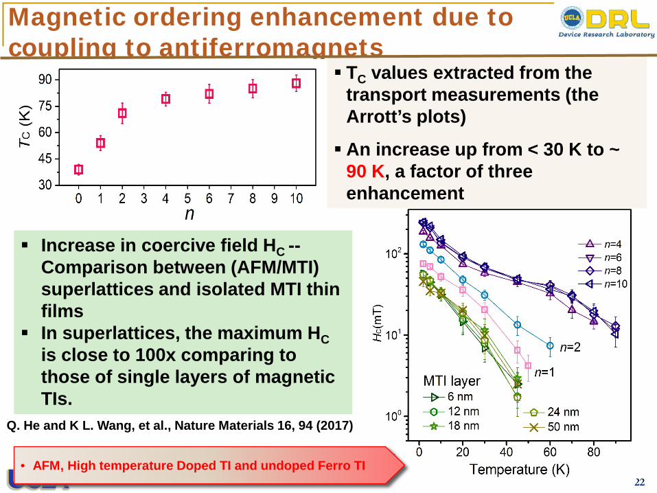
22
Magnetic ordering enhancement due to coupling to antiferromagnets
Increase in coercive field HC --Comparison between (AFM/MTI) superlattices and isolated MTI thin films
In superlattices, the maximum HCis close to 100x comparing to those of single layers of magnetic TIs.
Q. He and K L. Wang, et al., Nature Materials 16, 94 (2017)
TC values extracted from the transport measurements (the Arrott’s plots)
An increase up from < 30 K to ~ 90 K, a factor of three enhancement
• AFM, High temperature Doped TI and undoped Ferro TI

Summary and Outlook
Data Bus
ALUCache Memory
RegistersCPU
Software Programs
Microprocessor
Storage(nonvolatile)
Cache MemoryRegisters
KL Wang, et al., IEEE Proc. 104, 1976-2008, Oct 2016; J of Spin, 2, 1250009, 2012
Spintronics: Energy scaling Low dissipation, fast, high endurance, cost effective nonvolatile memory (& logic)
SOC engineering - Voltage write MeRAM low dissipation
Topological Spintronics
Metrology for accelerating the progress• VCMA, SOT, Skyrmions, etc..
Atomic scaling imaging, dynamics and understanding• XMCA, neutron, Magnetic probe, NV cell probe, Lorentz TEM, ..
Dense MemorySparse Logics
Cognitive systemsLow latency,
Cost effective
Neuro-morphicsystems
TI
Magnet
mz
< >
< >

24
Acknowledgements NSF, ARO, DOE EFRC Program SHINES, C-Spin &
FAME/DARPA, TANMS, for funding support All students and researchers Experimental collaborations
Prof. Jing Shi (UCR), Ilya Krivorotov (UCI), Caroline A. Ross (MIT), Wei-Li Lee (IOP), E. S. Choi (NHMFL), Elaine Li (UT Austin), Ming Zhong Wu (Colorado)
Theoretical collaborationsAllan MacDonald (UT Austin), Yaroslav Tserkovnyak (UCLA, So Takei (UCLA), Pramey Upadhyaya (UCLA), S. K. Kim (UCLA),Shoucheng Zhang (Stanford), Jing Wang (Stanford)
Thank you very much!
ARO
25
25 minutes and 5 minutes questions


![Spintronics [EDocFind.com]](https://img.pdfslide.us/doc/110x75/577d2e0b1a28ab4e1eaea99b/spintronics-edocfindcom.jpg)
