Embed Size (px)
Citation preview

13
Overview of Computational Methods for Photonic Crystals
Laurent Oyhenart and Valérie Vignéras IMS Laboratory, CNRS, University of Bordeaux 1
France
1. Introduction
A photonic crystal (PC) is a periodic structure whose refraction index of the material is periodically modulated on the wavelength scale to affect the electromagnetic wave propagation by creating photonic band gaps. In 1887, Lord Rayleigh is the first to show a band gap in one-dimensional periodic structures i.e. a Bragg mirror. In 1987, Eli Yablonovitch and Sajeev John have extended the band gap concept to the two and three-dimensional structures and for the first time, they use the term "photonic crystal" (Yablonovitch, 1987; John, 1987).
Progress in computational methods for the photonic crystals is understood through an historical review (Oyhenart, 2005). At the beginning of research in the photonic crystals, the purpose was to find a structure with complete band gap by improving the computational methods. In 1988, John shows theoretically by the scalar method of Korringa-Kohn-Rostoker (KKR) that the face centered cubic lattice (FCC) has a complete band gap between the second and the third band. One year later, Yablonovitch builds this structure and finds a band gap experimentally but the W-point raises a problem. In 1990, Satpathy et al. and Leung et al. confirm the complete band gap by the scalar plane wave method (PWM). A few months later, these two teams improve their methods to obtain vectorial PWM on D and E
fields. They find that FCC structure does not have complete band gap because W-point and U-point are degenerate. With these results, the editor of the journal "Nature" writes “Photonic Crystals bite the dust” (Maddox, 1990). Only two weeks later, Ho et al. created the vectorial PWM on H and they do not find the complete band gap in FCC structure but they show a complete band gap in the diamond lattice. In 1992, Sözuer et al. improve convergence of the PWM and they obtain a complete band gap for FCC lattice between 8th and 9th band. This structure that has caused many discussions has a complete band gap but not where it was expected.
To study and understand the propagation of the electromagnetic fields in the photonic crystals, computational methods were improved by using their symmetries and periodicities. We will study the classical methods for microwave devices such as the finite element method and the finite difference time domain. After some modifications of these methods, we obtain the band structure of PC which can be calculated by the methods from the solid state physics. For example the plane wave method, the tight binding method and the multiple-scattering theory will be studied. All these computational
www.intechopen.com
Photonic Crystals – Introduction, Applications and Theory
268
methods will be presented in this article and a PC example will be studied to compare these methods.
2. Equations, symmetries and periodicities in photonic crystals
2.1 Equations in photonic crystals
The Maxwell equations without sources control the electromagnetic wave propagation in PC.
, ,
, ,
, 0 , 0
t tt t
t t
t t
B r D rE r 0 H r 0
D r B r
(1)
In these laws, the same physical behavior is observed if we change simultaneously the
wavelength and the structure dimensions in the same proportions. Therefore, it is
convenient to introduce a normalized wavelength ┣0/a and a normalized frequency
af/c= a/┣0, with a the lattice constant of the photonic crystal (Joannopoulos et al., 2008).
Some methods do not solve the Maxwell equations directly but they use the Helmholtz equations, for example the E-wave equation or the H-wave equation:
2 2
0
1 2
0
r
r
k
k
E r E r r E r
r H r H r
with
,
,
i t
i t
t
t
e
e
E r E r
H r H r
(2)
Equations number to be solved depends on dimension of the photonic crystal. In the two-
dimensional case, the problem is simplified. It is assumed that the materials are uniform
along z-axis. It follows that the fields are uniform and the partial derivatives with respect to
the variable z vanish. The previous equation is simplified and split-up into TE-polarization
and TM-polarization; we have a scalar equation for each polarization:
2 2
2
02 2
for TE-polarizationwith
for TM-polarization0
z
r
z
F EF Fk
F Hx yF
r r
r r (3)
The computation time decreases exponentially compared to the three-dimensional case. In
the one-dimensional case, the problem is even more simplified. If the materials are uniform
along x-axis and y-axis, we solve analytically one second-order equation:
2
2
020
r
d Fk F
dz r
r r with , , or x y x y
F E E H H (4)
2.2 Symmetries of photonic crystals
Like all sets of differential equations, Maxwell's equations cannot be uniquely solved
without a suitable set of boundary conditions. Photonic crystals have symmetries which
define boundary conditions. Symmetries of the structure are not a sufficient condition to
reduce the computational domain; the electromagnetic field must be also symmetrical. On
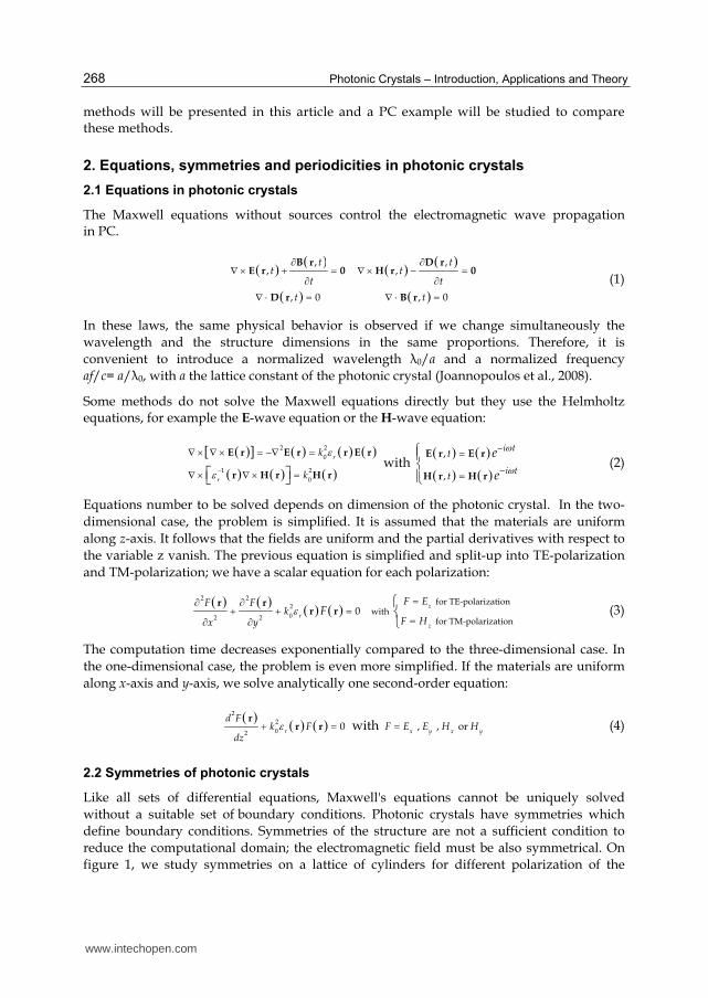
figure 1, we study symmetries on a lattice of cylinders for different polarization of the
www.intechopen.com
Overview of Computational Methods for Photonic Crystals
269
incident wave. In the first case, we apply a TM incident wave on the lattice with a horizontal
symmetry and the tangential magnetic field vanishes on the axis of symmetry. We put
perfect magnetic conductor (PMC) as boundary condition on the symmetry axis and we
study only half top or bottom of the problem. In the second case, we apply a TE incident
wave. Similarly, we reduce the problem with a perfect electric conductor condition (PEC).
Fig. 1. Both kinds of lateral symmetries
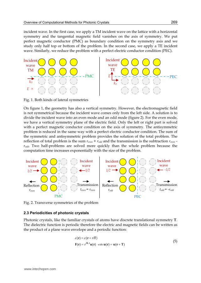
On figure 1, the geometry has also a vertical symmetry. However, the electromagnetic field is not symmetrical because the incident wave comes only from the left side. A solution is to divide the incident wave into an even mode and an odd mode (figure 2). For the even mode, we have a vertical symmetry plane of the electric field. Only the left or right part is solved with a perfect magnetic conductor condition on the axis of symmetry. The antisymmetric problem is reduced in the same way with a perfect electric conductor condition. The sum of the symmetric and antisymmetric problem provides the solution of the total problem. The reflection of total problem is the sum reven + rodd and the transmission is the subtraction reven - rodd. Two half-problems are solved more quickly than the whole problem because the computation time increases exponentially with the size of the problem.
Fig. 2. Transverse symmetries of the problem
2.3 Periodicities of photonic crystals
Photonic crystals, like the familiar crystals of atoms have discrete translational symmetry T.
The dielectric function is periodic therefore the electric and magnetic fields can be written as
the product of a plane wave envelope and a periodic function:
.
with
( ) ( )
( ) ( ) ( ) ( ) i
n
e
K r
r r T
F r u r u r u r T (5)
www.intechopen.com
Photonic Crystals – Introduction, Applications and Theory
270
The result above is commonly known as Bloch's theorem in solid state physics (Kittel, 2005).
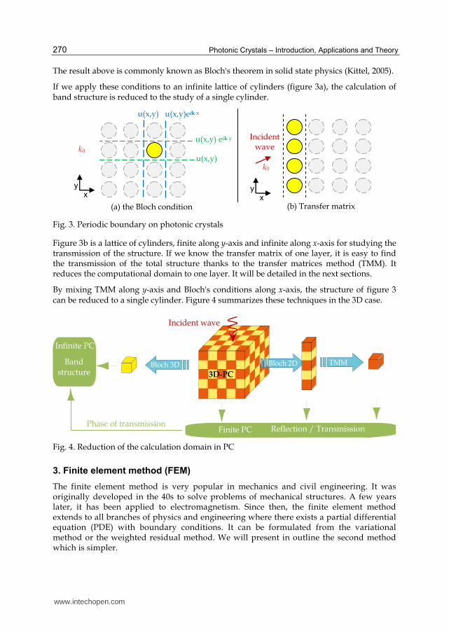
If we apply these conditions to an infinite lattice of cylinders (figure 3a), the calculation of band structure is reduced to the study of a single cylinder.
Fig. 3. Periodic boundary on photonic crystals
Figure 3b is a lattice of cylinders, finite along y-axis and infinite along x-axis for studying the transmission of the structure. If we know the transfer matrix of one layer, it is easy to find the transmission of the total structure thanks to the transfer matrices method (TMM). It reduces the computational domain to one layer. It will be detailed in the next sections.
By mixing TMM along y-axis and Bloch's conditions along x-axis, the structure of figure 3 can be reduced to a single cylinder. Figure 4 summarizes these techniques in the 3D case.
Fig. 4. Reduction of the calculation domain in PC
3. Finite element method (FEM)
The finite element method is very popular in mechanics and civil engineering. It was originally developed in the 40s to solve problems of mechanical structures. A few years later, it has been applied to electromagnetism. Since then, the finite element method extends to all branches of physics and engineering where there exists a partial differential equation (PDE) with boundary conditions. It can be formulated from the variational method or the weighted residual method. We will present in outline the second method which is simpler.
www.intechopen.com

Overview of Computational Methods for Photonic Crystals
271
Let us consider a partial differential equation with the differential operator of order n
applied to a function φ and a source function f:
f (6)
The first step is to expand the function φ on a set of functions:
1
N
j j
j
c
(7)
j are the chosen expansion functions and
jc are constant coefficients to be determined. The
best solution of the equation 6 is obtained when the residue r f is weakest on all points
of the domain . The weighted residual method requires this condition:
1
0N
i i j i j
j
R w rd c w f d
(8)
If we use the Galerkin method, the weight functions wi are the functions of previous interpolations and we write the problem in matrix form:
1
N
j ij i
j
c L b
with ij i jL d
and i ib fd
(9)
So now, we have to solve a linear system with cj unknowns where most of the entries of the matrix L are zero. Such matrices are known as sparse matrices, there are efficient solvers for such problems.
The basic idea of the finite element method is to divide the computation domain into small subdomains, which are called finite elements, and then use simple functions, such as linear and quadratic functions, to approximate the unknown solution over each element. For plane geometries, the domain is divided into finite triangular sub-domains. For three-dimensional problems, the sub-domains are tetrahedra. These two- and three-dimensional finite elements are widely used because it is a variable mesh and adapts to curved structures.
3.1 Transmission calculation of a photonic crystal
The finite element method usually solves the E-wave equation for PC (equation 5):
2
0 rk E r r E r (10)
For most of the finite elements computer programs, the frequency is fixed and the electric field is the unknown (Massaro et al., 2008). We use a commercial software, Ansys HFSS (High Frequency Structure Simulator). This three-dimensional computer program builds an adaptive tetrahedral mesh to model microwave devices, for example microstrips and antennas. These devices have a characteristic length lower than the wavelength of study. It is more difficult to study PC because it has a periodicity close to the wavelength and the matrix of calculation is large. To simplify calculations, we will study a periodic PC according to two directions of space. The directions where PC is infinitely periodic require
www.intechopen.com

Photonic Crystals – Introduction, Applications and Theory
272
to study only one period according to this direction. Several methods exist to model these conditions.
In the first method, the source is a plane wave and we use periodic boundary conditions
(PBC) on lateral faces and absorbing boundary conditions (ABC) on bases. We study only
one lateral period (figure 5). If the source has an oblique incidence, the phase shift is easily
taken into account by PBC because the E-field is a complex vector in FEM.
Fig. 5. Calculation of E-field in the PC with PBC, ABC and incident wave
The second method requires a very different source, a wave port. This source is a semi-
infinite waveguide whose cross section is drawn on bases of structure. Propagative modes
of this fictitious guide will be the source of the structure. For a plane wave source, we apply
to lateral faces and on the fictitious guide the conditions PEC and PMC (figure 6). The
source is transverse and has a normal incidence. It is not possible to change the angle of
incidence without change the boundary conditions of the lateral faces. The PC studied on
figure 5 can be reduced to quarter-spheres thanks to the symmetry of the fields at normal
incidence.
Fig. 6. Calculation of E-field in the PC with PEC, PMC and wave ports
3.2 Band structure calculation
The band structure shows the states which propagate in a PC. These states are differentiated
by their frequency and their Bloch wave vector. FEM sets the wave vector and solves the
wave equation to find the frequencies. There is no source, only boundary conditions to set
because it is an eigenvalue problem. In the case of a cavity resonator, the boundary
conditions of the domain are PEC. Whereas, for PC, we choose the Bloch conditions on all
faces of the unit cell to set the wave vector. The phase shift of the Bloch conditions is set
easily because the fields are complex vectors. The FEM calculates the band structure of
dielectric with or without losses, metallic, and metallodielectric PC. Any material can be
used by this method, it is the main advantage.
In this chapter, we choose a photonic crystal to study, a cubic lattice with several layers of
dielectric spheres which have a permittivity equal to 5.1 and radius equal to 0.4*a (a: lattice
Wave port2 Source
Wave port1
Lateral boundary conditions: PEC on up and down faces PMC on left and right faces
ABABC
k0
E
PBC on lateral faces
Source: incident wave
www.intechopen.com

Overview of Computational Methods for Photonic Crystals
273
constant). For the band structure, the number of layer is infinite, and for transmission
calculation, we study four and eight layers. The structure is deliberately simple to be
studied by all the methods. The band structure, the transmission coefficient in normal
incidence and some modes of dielectric PC are plotted on figure 7. For normal incidence, the
first two band gaps are found in the band structure and transmission curves.
The first method with incident waves takes about 7 hours and 960 Mo of working memory
on a personal computer to calculate the transmission of 8 layers i.e. 8 spheres. Whereas if we
use the second method with the wave ports, the memory is reduced to 360 Mo and the CPU
time is reduced to 8 min. To obtain this optimization, we reduced the geometry to four
quarter-spheres thanks to symmetries and we use the Padé interpolation on frequencies. It is
necessary to make optimizations if you want to use FEM.
Fig. 7. Band structure and transmission coefficient of dielectric PC
4. Finite-difference time-domain method (FDTD)
Finite difference method is a numerical method for approximating differential equations
using finite difference equations to approximate derivatives. This is very simple
to implement but it has some limitations in the mesh geometries. In 1966, Yee proposed a
finite difference scheme applied to electromagnetism. The FDTD was born (Taflove &
Hagness, 2005). The success of this method is due to the scheme based on the Taylor series
of second-order. For example, this method is used to model the effects of cellphones on the
human body, antennas and printed circuits. The FDTD uses the two structural equations of
Maxwell in a conducting, isotropic and homogeneous medium:
1
1
t
t µ
EH E
HE
(11)
www.intechopen.com
Photonic Crystals – Introduction, Applications and Theory
274
The FDTD uses an approximation of derivatives by centered finite differences.
2
2
i ii
i
u x h u x hdu x h
dx h (12)
Let us apply this approximation to one-dimensional case in order to understand the FDTD principle. The E and H-field are stepped in time and space. By replacing curls and derivatives, we obtain one-dimensional Yee scheme:
1/2 1/21/2 1/2
1 1/2 1/21/2 1/2 1
with
1
1
n nn nk kk k
n n n nk k k k
H HE E
t x
E E H H
t x
( . , ) ( , )
( . , ) ( , )
nk
nk
E E n t k x E t x
H H n t k x H t x
(13)
The E and H-field are staggered and updated step by step in time. E-field updates are conducted midway during each time-step between successive H-field updates, and conversely. This explicit time-stepping scheme avoids the need to solve simultaneous equations, and furthermore it is order N i.e. proportional to the size of the system to model. This scheme can be generalized for two-dimensional and three-dimensional problems. The Yee scheme is stable if the wave propagates from one cell to another with a speed less than the light (the Current-Friedrichs-Lewy condition).
4.1 Calculation of transmission coefficient
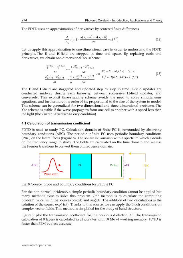
FDTD is used to study PC. Calculation domain of finite PC is surrounded by absorbing boundary conditions (ABC). The periodic infinite PC uses periodic boundary conditions (PBC) on the lateral faces (Figure 8). The source is Gaussian with a spectrum which extends on the frequency range to study. The fields are calculated on the time domain and we use the Fourier transform to convert them on frequency domain.
Fig. 8. Source, probe and boundary conditions for infinite PC
For the non-normal incidence, a simple periodic boundary condition cannot be applied but many methods exist to solve this problem. One method is to calculate the computing problem twice, with the sources cos(t) and sin(t). The addition of two calculations is the solution of the source exp(-it). Thanks to this source, we can apply the Bloch conditions on complex vector fields. This method is simplified for the study of band structure.
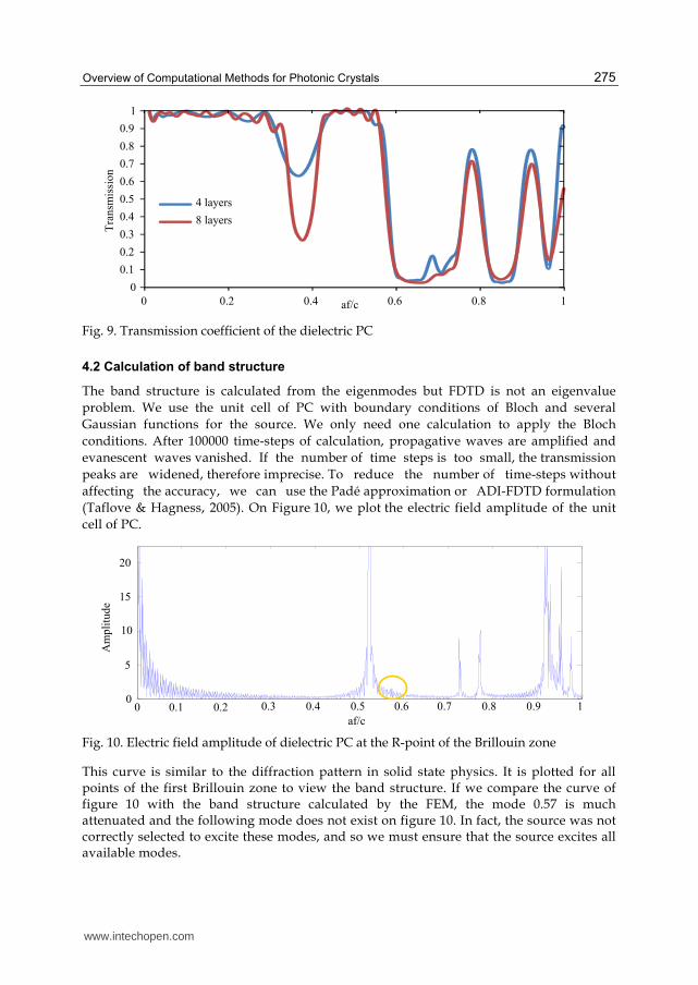
Figure 9 plot the transmission coefficient for the previous dielectric PC. The transmission calculation of 8 layers is calculated in 32 minutes with 58 Mo of working memory. FDTD is faster than FEM but less accurate.
PBC Probe PC
Plane wave
ABC ABC
www.intechopen.com
Overview of Computational Methods for Photonic Crystals
275
Fig. 9. Transmission coefficient of the dielectric PC
4.2 Calculation of band structure
The band structure is calculated from the eigenmodes but FDTD is not an eigenvalue
problem. We use the unit cell of PC with boundary conditions of Bloch and several
Gaussian functions for the source. We only need one calculation to apply the Bloch
conditions. After 100000 time-steps of calculation, propagative waves are amplified and
evanescent waves vanished. If the number of time steps is too small, the transmission
peaks are widened, therefore imprecise. To reduce the number of time-steps without
affecting the accuracy, we can use the Padé approximation or ADI-FDTD formulation
(Taflove & Hagness, 2005). On Figure 10, we plot the electric field amplitude of the unit
cell of PC.
Fig. 10. Electric field amplitude of dielectric PC at the R-point of the Brillouin zone
This curve is similar to the diffraction pattern in solid state physics. It is plotted for all points of the first Brillouin zone to view the band structure. If we compare the curve of figure 10 with the band structure calculated by the FEM, the mode 0.57 is much attenuated and the following mode does not exist on figure 10. In fact, the source was not correctly selected to excite these modes, and so we must ensure that the source excites all available modes.
0 0.1 0.2 0.3 0.4 0.5 0.6 0.7 0.8 0.9 1 0
5
10
15
20
Am
pli
tud
e
0
0.1
0.2
0.3
0.4
0.5
0.6
0.7
0.8
0.9
1
0 0.2 0.4 0.6 0.8 1
Tra
nsm
issi
on
af/c
4 layers
8 layers
af/c
www.intechopen.com

Photonic Crystals – Introduction, Applications and Theory
276
5. Finite-difference frequency-domain method (FDFD)
We will study a finite difference method combined with transfer matrix method and the
Fourier transform. The finite difference method substitutes the derivatives in PDE to obtain
finite difference schemes. In electromagnetism, FDFD uses the structural equations of
Maxwell on space (k, ) and applies approximations on the wave vector:
0
with
1 /
1 /
1 /
x
y
z
ik ax
ik b
y
ik cz
k e ia
k e ib
k e ic
k E H
k H E (14)
a,b,c are lattice constants along x, y and z-axis. We obtain discrete equations which are
applied to one layer of the structure on a cubic lattice. In 1992, Pendry and MacKinnon
(Pendry & MacKinnon, 1992) used this method with transfer matrix method (TMM) which
extended the solution of one layer to the total structure. To apply TMM, the discrete
equations must be written on real space. We obtain a set of equations where z-component of
the E and H-fields can be removed. The six equations are reduced to four equations which
are written in a matrix form:
Tˆ , with
r
x y x yc E E H H
F r T r r F r F r r r r r (15)
5.1 Calculation of band structure
The band structure is calculated from unit cell of structure by setting frequency and
calculating wave vectors propagating in the unit cell. Bloch's theorem applies to vector F:
x
y
z
ik a
ik b
ik c
a e
b e
c e
F r F r
F r F r
F r F r
(16)
and' , ' 'a a b b c c are the mesh size along x, y and z-axis. The transfer matrix of
the unit cell is written from the unit mesh:
1
1
withˆ ˆ ˆ,0 ,0 , N
j j
r j
c c c F r T F r T T r r (17)
If the above equations are joined together, we have an eigenvalue problem:
ˆ ,0 zik c
r
c e
T F r F r (18)
We set the wave number k and the wavelength k0 to solve the eigenvalue problem. The
eigenvalues kz having an imaginary part are eliminated because they are not propagating
waves. The remaining eigenvalues gives us the band structure kz(k0).
www.intechopen.com

Overview of Computational Methods for Photonic Crystals
277
5.2 Calculation of transmission coefficient
The reflection and transmission calculation is performed using the transfer matrices. It is more interesting to calculate the elements of transmission matrix than the transmitted field in some points. The incident, reflected and transmitted waves are expanded on a plane-wave basis sets thanks to the transfer matrices.
ˆ0
T is the transfer matrix of a vacuum layer. The eigenvectors of ˆ0
T define a plane-wave
basis set:
ˆ
ˆ
i
i
ik ci i
ik ci i
r e r
l e l
0
0
T
T (19)
The right and left eigenvectors are different because ˆ0
T operator is not self-adjoint. They are
expanded on the reciprocal space kx and ky and translate on the direct space with the Fourier
transform because the transfer matrix is known in direct space. kz is found easily because we
are in a vacuum layer. The transfer matrix T is not compatible with the new plane-wave
basis set, we convert this matrix:
ˆj i j i i j jil r l T r T l r T
T (20)
To calculate the transmission coefficient, this matrix is arranged to group the eigenvectors with the same propagation direction. This matrix is divided into four blocks:
11 12
21 22
T T
TT T
(21)
TMM calculates the transmission coefficient of several layers from one layer (see 1D-MST). A great number of layers can be calculated without increasing the computing power.
Figure 11 plot the band structure and the transmission coefficient calculated by FDFD, for the previous dielectric PC. If we compares with figure 7, the first bands are correct but inaccuracies on the higher band after 0.6-frequency are due to the weak mesh (7x7x7 cells). If we increase the number of cells, accuracy increases. Calculation is more difficult for high frequencies because the E- and H-field are functions that oscillate more. The transmission calculation of 8 layers is calculated in 22 seconds with 3.3 Mo of working memory for 7x7x7 cells. The computing time is low because only one sphere is actually calculated thanks TMM.
6. Finite Integration Technique (FIT)
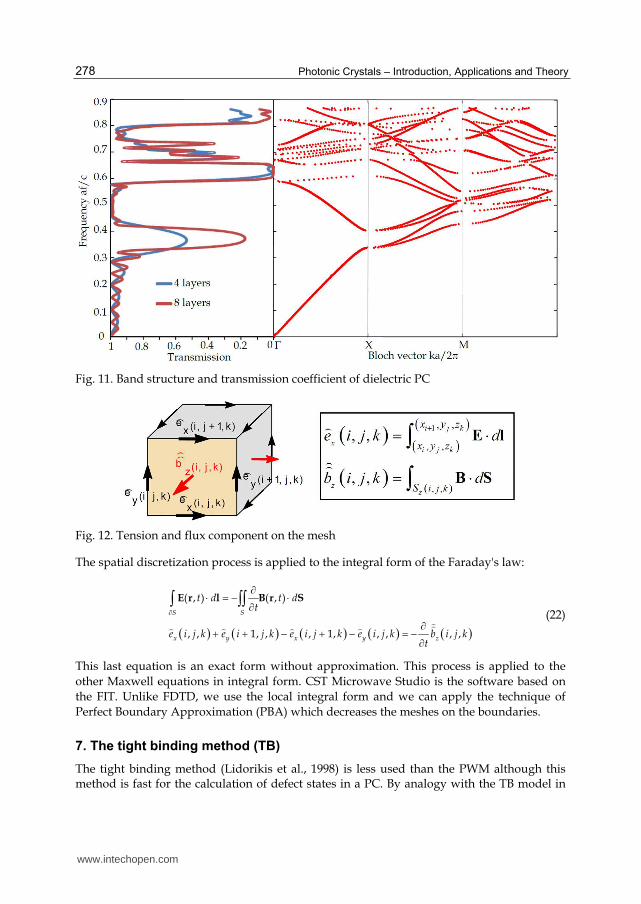
In 1977, Weiland proposes a spatial discretization scheme to solve the integral equations of Maxwell (Weiland, 1977). This scheme called Finite Integration Technique (FIT) can be applied to many electromagnetism problems, in time and frequency domain, from static up to high frequency. The basic idea of this approach is to apply the Maxwell equations in integral form to a set of staggered grids like FDTD (figure 12).
www.intechopen.com
Photonic Crystals – Introduction, Applications and Theory
278
Fig. 11. Band structure and transmission coefficient of dielectric PC
Fig. 12. Tension and flux component on the mesh
The spatial discretization process is applied to the integral form of the Faraday's law:
( , ) ( , )
, , 1, , , 1, , , , ,
S S
x y x y z
t d t dt
e i j k e i j k e i j k e i j k b i j kt
E r l B r S
(22)
This last equation is an exact form without approximation. This process is applied to the
other Maxwell equations in integral form. CST Microwave Studio is the software based on
the FIT. Unlike FDTD, we use the local integral form and we can apply the technique of
Perfect Boundary Approximation (PBA) which decreases the meshes on the boundaries.
7. The tight binding method (TB)
The tight binding method (Lidorikis et al., 1998) is less used than the PWM although this method is fast for the calculation of defect states in a PC. By analogy with the TB model in
www.intechopen.com
Overview of Computational Methods for Photonic Crystals
279
solid-state physics, H-field is expanded on localized wave functions. They are calculated from the Wannier functions an(R,r) for a PC without defect:
1
2
32
, ( , )2
in n
BZ
e d k R
a R r H k r k (23)
The Wannier functions are a complete set of orthogonal functions which is defined for each band and each unit cell. The Wannier functions only depend on the quantity (r-R), r is the space position and R is any lattice vector. The reverse relation is written as follows:
12
32
( , ) ,2
in n e
k R
G
H k r a R r (24)
Hn(k,r) functions are the eigenvectors of H-wave equation. PWM solve this equation to get the Hn(k,r) functions for the PC without defect. To study a defect in PC, the H-field is expanded on the previous Wannier functions:
( ) ,n n
n
cR
H r R a R r (25)
Green's functions method solve the H-wave equation for the photonic crystal with defect.
8. Plane Wave Method (PWM)
Plane wave method is used to study the band structure of PC. It comes from the solid state physics where the electronic wave functions are scalar whereas the electromagnetic fields are vectors. A scalar approximation of fields is not enough to describe band structure. This method is modified to take the vectorial nature of the fields into account. Three computational methods of vectorial PWM were created quasi-simultaneously: the E-field method (Leung & Liu, 1990), the D-field method (Zhang & Satpathy, 1990) and the H-field method (Ho et al., 1990). The D and H-field are continuous in PC unlike the E-field. Moreover, only the differential operators of the wave equation on E-field and H-field are self-adjoint. We present the H-field method because of these properties. PWM expands the field and permittivity on plane-wave basis set. The permittivity is a periodic function with translational symmetry T, so Bloch's theorem can be applied to the H-field:
with.
( ) ( ) ( ) ( )ie K rH r h r h r h r T (26)
All periodic functions can be expanded on reciprocal space with Fourier series:
.
.
( )
( )
ir
i
e
e
G r
G
G
G r
G
G
r
h r h
(27)
The H-field is written:
www.intechopen.com

Photonic Crystals – Introduction, Applications and Theory
280
. .
, 1,2
ˆ( )i i
e h e
K G r K G r
G G K G
G G
H r h e (28)
As the H-field is transverse, each plane wave is perpendicular to the propagation vector
K+G. The transverse plane of the propagation vector is described by the unit vectors 1ˆ K Ge
and 2ˆ K Ge . The set of vectors 1 2ˆ ˆ, ,
K G K Ge e K G represents an orthonormal basis. We only
need to storage two vectors instead of three, consequently data storage is reduced. The
Fourier series expansion is replaced in the H-wave equation:
1 20
. .1 . 20
, ,
ˆ ˆ
r
i ii
k
e h e k h e
K G r K G rG r
G G K G G K G
G G G
r H r H r
e e
(29)
Some algebraic calculations simplify this equation and we get for every vector G, the central equation of the photonic crystals:
1 20
,
ˆ ˆ h k h
G G K G K G G G
G
K G e K G e (30)
This equation is an eigenvalue problem which is solved with classical methods. The Bloch vector K is set and we try to find the eigenvalues k0. The calculation convergence depends on the N number of reciprocal lattice vectors G. A minimum number of vectors G is necessary to describe correctly the permittivity of the PC. The convergence of the problem is rather slow. As the H-field is transverse, the number of equations is decreased from 3N to 2N. The PWM is difficult to apply to the materials whose permittivity depends on the frequency like metals. On figure 13, we plot the band structure of the dielectric PC. It is calculated in 12 seconds with 10 Mo of working memory for 343 plane-waves. Calculation is fast because the structure is simple. If we compares with figure 7, we obtain the same result.
Fig. 13. Band structure of the previous dielectric PC
X M R
0
0.1
0.2
0.3
0.4
0.5
0.6
0.7
0.8
0.9
1
ka / 2
k0a
/ 2
www.intechopen.com
Overview of Computational Methods for Photonic Crystals
281
8.1 One and two-dimensional photonic crystals
If we study one or two-dimensional PC, the central equation is written in another form and will be simplified:
2 2 2 1
201 2 1 1
1 11
2 2
ˆ ˆ ˆ ˆ
ˆ ˆ ˆ ˆk
h h
h h
K G K G K G K G
K G K G K G K G
G G
G G
G G G
e e e e
e e e e
K G K G (31)
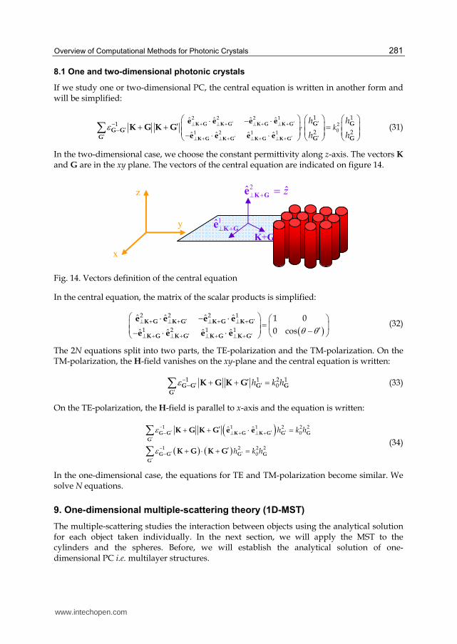
In the two-dimensional case, we choose the constant permittivity along z-axis. The vectors K and G are in the xy plane. The vectors of the central equation are indicated on figure 14.
Fig. 14. Vectors definition of the central equation
In the central equation, the matrix of the scalar products is simplified:
2 2 2 1
1 2 1 1
ˆ ˆ ˆ ˆ 1 0
0 cosˆ ˆ ˆ ˆ
K G K G K G K G
K G K G K G K G
e e e e
e e e e
(32)
The 2N equations split into two parts, the TE-polarization and the TM-polarization. On the TM-polarization, the H-field vanishes on the xy-plane and the central equation is written:
1 1 2 10h k h
G G G G
G
K G K G (33)
On the TE-polarization, the H-field is parallel to x-axis and the equation is written:
1 1 1 2 2 20
1 2 2 20
ˆ ˆ h k h
h k h
G G K G K G G G
G
G G G G
G
K G K G e e
K G K G
(34)
In the one-dimensional case, the equations for TE and TM-polarization become similar. We solve N equations.
9. One-dimensional multiple-scattering theory (1D-MST)
The multiple-scattering studies the interaction between objects using the analytical solution for each object taken individually. In the next section, we will apply the MST to the cylinders and the spheres. Before, we will establish the analytical solution of one-dimensional PC i.e. multilayer structures.
x
z 2ˆ z
K Ge
K+G
1ˆ K Ge y
www.intechopen.com
Photonic Crystals – Introduction, Applications and Theory
282
9.1 Transfer-matrix method (TMM)
Transfer-matrix method is known since many years (Born & Wolf, 1999). It is essential for the study of PC. TMM reduces the computational domain. In this section, transfer matrix will be applied to one-dimensional PC. For oblique incidences, we solve the E-wave equation for TE-polarization and the H-wave equation for TM-polarization. Two polarizations are separated and we use the same steps of calculation for two polarizations. We will study only the E-wave equation:
2 20 0rk E r r E r (35)
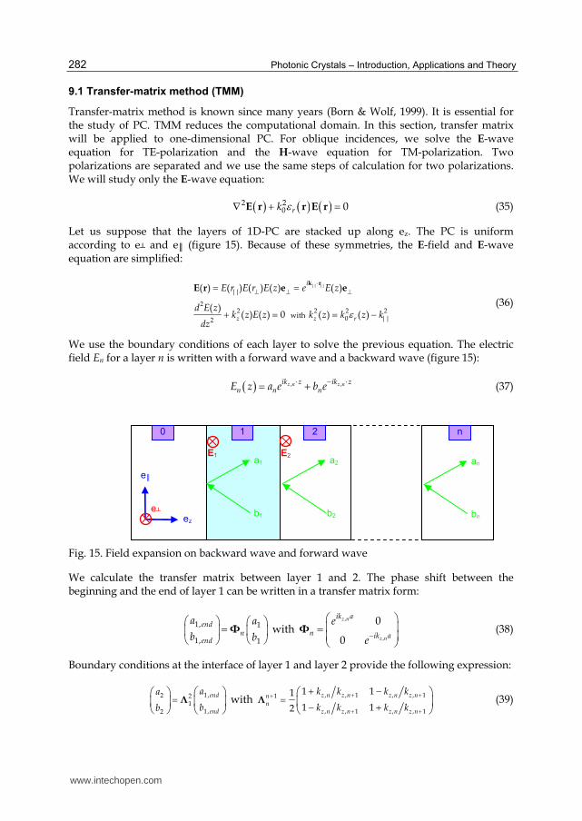
Let us suppose that the layers of 1D-PC are stacked up along ez. The PC is uniform according to e┴ and e║ (figure 15). Because of these symmetries, the E-field and E-wave equation are simplified:
|| ||
||
22 2 2 2
0 ||2with
( ) ( ) ( ) ( ) ( )
( )( ) ( ) 0 ( ) ( )
i
z z r
E r E r E z e E z
d E zk z E z k z k z k
dz
k rE r e e
(36)
We use the boundary conditions of each layer to solve the previous equation. The electric field En for a layer n is written with a forward wave and a backward wave (figure 15):
, ,z n z nik z ik zn n nE z a e b e
(37)
Fig. 15. Field expansion on backward wave and forward wave
We calculate the transfer matrix between layer 1 and 2. The phase shift between the beginning and the end of layer 1 can be written in a transfer matrix form:
1, 1
1, 1
endn
end
a a
b b
Φ with ,
,
0
0
z n
z n
ik a
n ik a
e
e
Φ (38)
Boundary conditions at the interface of layer 1 and layer 2 provide the following expression:
1,2 2
11,2
end
end
aa
bb Λ with
, , 1 , , 11
, , 1 , , 1
1 11
1 12
z n z n z n z nnn
z n z n z n z n
k k k k
k k k k
Λ (39)
a2
b2
E2
e║
ez
E1
0 1 n 2
e┴
an
bn
a1
b1
www.intechopen.com

Overview of Computational Methods for Photonic Crystals
283
The product of previous matrices provides the transfer matrix from layer 1 to layer 2:
2 1 11 12 2
1 12 1 21 22
with .a a T T
b b T T T T Λ Φ (40)
The transmission of the layer is calculated from inversion of transfer matrix. The inverse will be calculated directly from phase shift matrices and interface matrix to avoid inaccuracies:
111 2 221 1
1 2 2
1 a a a
b b b
T Φ Λ (41)
The following equation converts the transfer matrix to scattering matrix:
1 1 1 1 1
1 11 12 1 21 11 22 12 21 1
1 12 21 22 2 211 12
1
1
b S S a T T T T T a
a S S b bT T
(42)
Reflection and transmission coefficients are equal respectively to:
1
2111 211 1
11 11
1
TS S
T T
(43)
Several layers are calculated similarly.
9.2 Kronig-Penney model
The Kronig-Penney model evaluates the electronic levels of a crystal structure in a one-dimensional periodic potential (Kittel, 2005). This model has been modified to be used in PC and takes into account the oblique incidences (Mishra & Satpathy, 2003). We use TMM and the field expansion on backward and forward wave. The structure is periodic according to z-axis (figure 16).
Fig. 16. Refraction index of one dimensional PC
a1
b1
a2
b2
z
n(z)
0 a
E1 E2
a
www.intechopen.com
Photonic Crystals – Introduction, Applications and Theory
284
The field E(z) of the previous section is a Bloch function on z. The continuity of tangential fields and the Bloch theorem give the two following relations:
2 1
2 1
0
( ) (0)iKa
iKa
a
E a e E
dE dEe
dz dz
(44)
K is the wave vector of Bloch. In the unit cell, the permittivity is not uniform according to z-axis. It is splitted into sub-cells with a constant permittivity. We calculate the transfer matrix of the unit cell from the expressions of the previous section:
2 11 12 1
2 21 22 1
a T T a
b T T b (45)
We expand equation 44 on forward and backward waves:
2 2 1 1
2 2 1 1
iKa
iKa
a b e a b
a b e a b
(46)
Equation 46 is replaced in equation 45:
11 12 1 1
21 22 1 1
= iKaT T a a
eT T b b
(47)
The Bloch factor eiKa and the complex conjugate value e-iKa are the two eigenvalues of the transfer matrix because the determinant of this matrix is equal to one. The trace of the transfer matrix is equal to the sum of the eigenvalues:
11 22iKa iKa
T T e e (48)
If the materials of the photonic crystal do not absorb, we have *11 22T T . Similarly to the
Kronig-Penney model, the above relation is written from the transmission coefficient:
21
21 21
1 1*21 21 11 22
21 21
S
S S
i
i i
iKa iKa
S S e T T
e ee e
S S
(49)
After simplification, the transcendent equation is written:
21
21
coscos
SKa
S
(50)
We get an equation similar to electronic case. The transmission coefficient is different in the TE and TM-polarization. To plot band structure f( k║,K, k0) = 0, we set the wave numbers k0 and k║ and calculate the Bloch number K.
www.intechopen.com

Overview of Computational Methods for Photonic Crystals
285
10. Two-dimensional multiple-scattering theory (2D-MST)
The multiple-scattering is an analytical theory which calculates the scattering of N objects from the scattering of each object independently (Felbacq et al., 1994). In the two-dimensional case, objects are cylinders and the theory uses the scalar wave equation:
2 2 2 1 rE k E k E r r r r (51)
Outside the cylinders, the wave equation can be split into two equations, one for the incident field E0 and the other one for the scattered field Es:
0
2 20 0
2 2 2
0
1
s
s s r
E E E
E k E
E k E k E
r r r
r r
r r r r
(52)
Using Green's theorem, the scattered field outside the cylinder can be written as follows:
2
14
s r
ikE H k E dS r r r r r (53)
The function H is a Hankel function. The surface integral can be restricted to the Cj cylinders. The scattered field is written as a sum:
2 1
4 j
js s
j
jrj
s C
E E
ikE H k E dS
r r
r
r r r r
(54)
The cylinders interact to give the scattered field by the structure. To better understand the process of multiple-scattering between the cylinders, we will study a simple example of cylinders with circular section aligned along x-axis and excited by an incident field propagating along x-axis (figure 17).
Fig. 17. Incident field on n cylinders aligned
The incident field is expanded into Bessel functions:
0 0ikx l
l l ll l
E e i J kr a J kr r (55)
We define the total incident field around the cylinder i which takes into account other cylinders:
C1
y
C2 Cn
x
E
…
www.intechopen.com
Photonic Crystals – Introduction, Applications and Theory
286
ii il l
l
E a J krr (56)
In the case of the cylinders with circular section, the integral 54 is calculated analytically:
(1)js jl l
l
E b H krr with jl jl jlb S a (57)
Sjl is the scattering coefficients (Bohren & Huffman, 1998). The field jsE r scattered by a
cylinder j is shifting on another cylinder i to become an incident field Gjil.bjl on this cylinder
with Gjil the translation coefficients (Felbacq et al., 1994). If we shift all the scattered fields
on the cylinder i, and if we add the initial incident field to it, we get the total incident field
on the cylinder i:
0il jil jl lj i
a G b a
(58)
By using the equation 57, we get the multiple-scattering equation:
0il jil jl jl lj i
a G S a a
(59)
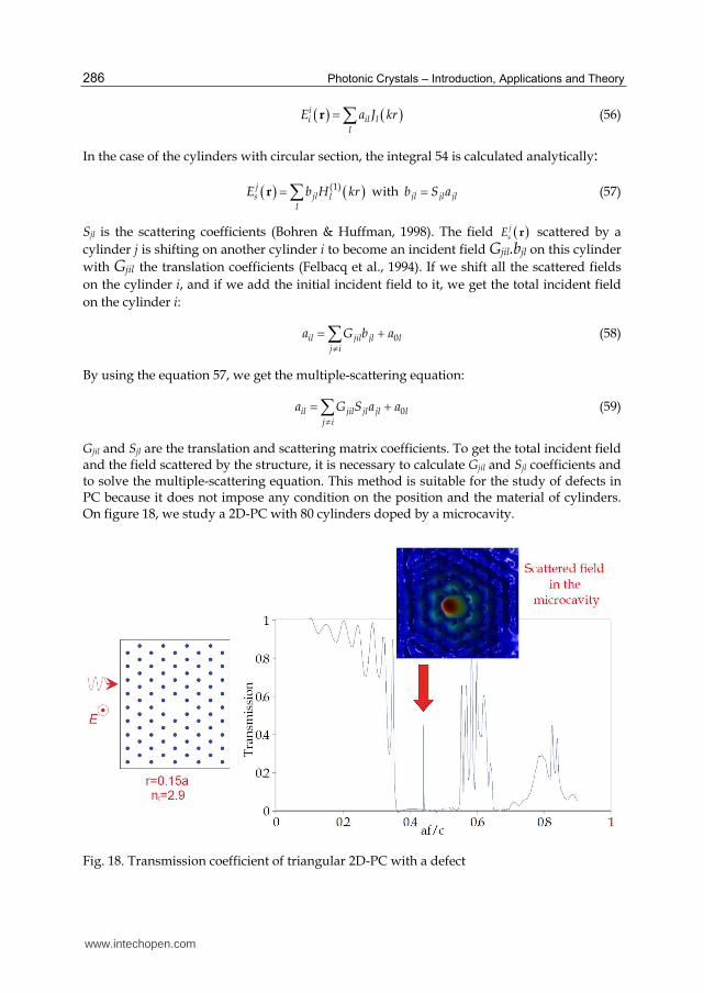
Gjil and Sjl are the translation and scattering matrix coefficients. To get the total incident field and the field scattered by the structure, it is necessary to calculate Gjil and Sjl coefficients and to solve the multiple-scattering equation. This method is suitable for the study of defects in PC because it does not impose any condition on the position and the material of cylinders. On figure 18, we study a 2D-PC with 80 cylinders doped by a microcavity.
Fig. 18. Transmission coefficient of triangular 2D-PC with a defect
www.intechopen.com
Overview of Computational Methods for Photonic Crystals
287
11. Three-dimensional multiple-scattering theory (3D-MST)
The three-dimensional multiple-scattering theory use same principles as the two-dimensional case but three-dimensional case is more complex because the Helmholtz equation is vectorial. The 3D-MST is separated into two parts, the calculation for one sphere and the generalization to N spheres (Oyhenart & Vignéras, 2007). The first part calculates the scattered wave by one sphere with Mie theory. The base of spherical harmonics is written as follows:
1, ,
1, , 1
4( ) ,
1
ˆ
l
l m l lm
l m M
iz kr Y
i l l
i
k
Z r
Z Z
(60)
Zl are the Hankel and Bessel spherical functions and ,lm
Y are scalar spherical wave
functions. The incident field and the scattered field are expanded on spherical wave
functions:
0 (1)0 , , , ,
, ,
(3) 0, , , , , , , ,
, ,
with
( )
l m l m
l m
s ss l m l m l m l l m
l m
E
E E S E
r Z
E Z
E
(61)
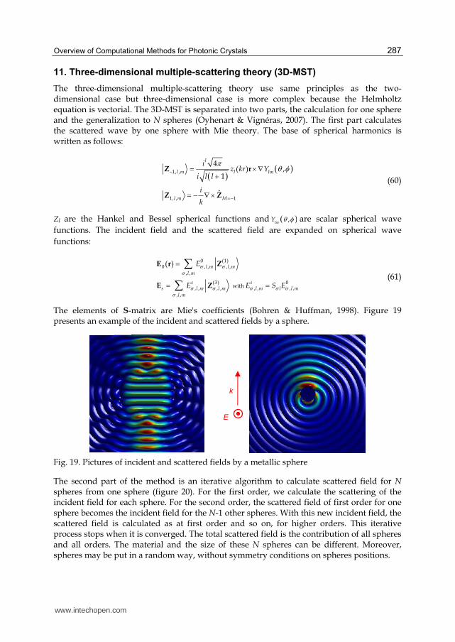
The elements of S-matrix are Mie's coefficients (Bohren & Huffman, 1998). Figure 19 presents an example of the incident and scattered fields by a sphere.
Fig. 19. Pictures of incident and scattered fields by a metallic sphere
The second part of the method is an iterative algorithm to calculate scattered field for N spheres from one sphere (figure 20). For the first order, we calculate the scattering of the incident field for each sphere. For the second order, the scattered field of first order for one sphere becomes the incident field for the N-1 other spheres. With this new incident field, the scattered field is calculated as at first order and so on, for higher orders. This iterative process stops when it is converged. The total scattered field is the contribution of all spheres and all orders. The material and the size of these N spheres can be different. Moreover, spheres may be put in a random way, without symmetry conditions on spheres positions.
E
k
www.intechopen.com

Photonic Crystals – Introduction, Applications and Theory
288
These two last remarks show all the interest of this method in calculation of PC with defects and random structures.
Fig. 20. Block diagram of multiple-scattering method, the total scattered field is the sum of the scattered fields for all orders.
For periodic structures, calculation is simplified. Figure 21 plot the transmission coefficient for the previous infinite dielectric PC. The transmission calculation of 8 layers is calculated in 11 minutes with 63 Mo of working memory. By using the principle of KKR-method of
solid state physics, MST can also calculate the band structure (Wang and Al, 1993). MST
is the fastest method for the finite structures and random structures.
Fig. 21. Transmission coefficient of the infinite periodic dielectric PC
www.intechopen.com

Overview of Computational Methods for Photonic Crystals
289
12. Conclusion: Comparison of computational method
The computational methods are studied and compared on table 1. The first four methods are
three-dimensional numerical methods coming from electromagnetism. The FEM gives very
precise results but it requires many resources systems. Another method, the FDTD is very
used and converges without an excessive mesh thanks to its formulation. If you want more
precise results, the mesh becomes heavy and you need to use FEM. The FDFD studies
photonic crystals with a high number of layers by modeling only one layer. The FIT is a
method which studies numerically PC with a high number of objects, without holding
excessive resources system but the result is approximate. These methods calculate dielectric
and metallic PC to obtain reflection and transmission coefficients and the band structure.
Then, we have others methods resulting from the solid state physics which require a very
small computing time. They were adapted from the scalar methods of the solid state
physics. The PWM calculate only the band structure. The tight binding method is less used
than the PWM although this method is fast for the calculation of defect states in a PC. The
multiple-scattering theory which is also used in optics studies analytically large finite PC
and it easily takes the defects into account in the PC. For three-dimensional PC, there is
no simple method, fast and accurate. We must remove a feature. For example, the 3D-
MST is fast and accurate but the computer program is complex to write.
FEM FDTD FDFD FIT TB PWM 1D-MST 2D-MST 3D-MST
Origin E.M. E.M. E.M. E.M. Q.M. Q.M. Q.M. E.M. both
Maxwell's equations Freq. Time Freq. Time Freq. Freq. Freq. Freq. Freq.
Calculation Num. Num. Num. Num. Num. Num. Analyt. Analyt. Analyt.
Geometries 3D 3D 3D 3D 2D/3D 3D 1D Cyl. Sphere
Discrete equations X X X X
Expansion, series X X X X X X
Free space, finite PC X X X X X X
Infinite periodic PC X X X X X X X X
Band structure X X X X X X X X
Transmission/reflection X X X X X X X
Metallic PC X X X X X
Single defect in finite-PC X X X X X X
Periodic defect X X X X X X X X X
computing speed slow med. fast fast fast med. fast fast fast
data storage large low low low low low low low low
commercial software X X X
Free software X X X X X X
Popular method in PC X X X
Abbreviations: Q.M. : quantum mechanics and solid state physics E.M. : electromagnetism Freq. : frequency domain Time : time domain
Analyt. : analytical method Num. : numerical method Med. : medium Cyl. : cylinder
Table 1. Specifications of the computational methods
www.intechopen.com

Photonic Crystals – Introduction, Applications and Theory
290
13. References
Bohren, C.F. & Huffman, D. R. (1998). Absoption and scattering of light by small particles, Wiley, ISBN: 978-0-471-29340-8, New-York, USA
Born, M. & Wolf, E. (1999). Principles of optics (7th edition), Cambridge Press, ISBN 0521642221, Cambridge, United Kingdom
Felbacq, D.; Tayeb, G. & Maystre, D. (1994). Scattering by a random set of parallel cylinders, J. Opt. Soc. Am. A, Vol.11, No. 9, (September 1994) pp. 2526-2538
Ho, K.M.; Chan, C.T. & Soukoulis, C.M. (1990). Existence of a Photonic Gap in Periodic Dielectric Structures, Phys. Rev. Lett., Vol.65, No.25, (December 1990), pp. 3152-3155
Joannopoulos, J.D.; Johnson, S.J.; Winn, J.N. & Meade, R.D. (2008). Photonic crystals: molding the flow of light, Princeton University Press, ISBN: 9780691124568, Princeton, USA
John, S. (1987). Strong localization of photons in certain disordered dielectric superlattices, Phys. Rev. Lett., Vol.58, No.23, (June 1987) pp. 2486-2489
Kittel, C. (2005). Introduction to Solid State Physics (8th edition), Wiley, ISBN 978-0-471-41526-8, New-York, USA
Leung, K.M. & Liu, Y.F. (1990). Full Vector Wave Calculation of Photonic Band Structures in Face-Centered-Cubic Dielectric Media, Phys. Rev. Lett., Vol.65, No.21, (November 1990), pp. 2646-2649
Lidorikis, E.; Sigalas, M.M.; Economou, E.N. & Soukoulis, C.M. (1998). Tight-Binding Parametrization for Photonic Band Gap Materials, Phys. Rev. Lett., Vol.81, No.7, (August 1998) pp. 1405-1408
Maddox, J. (1990). Photonic Band-Gaps Bite the Dust. Nature, Vol.348, (December 1990), pp. 481
Massaro, A.; Errico, V.; Stomeo, T.; Salhi, A.; Cingolani,R.; Passaseo, A. & DeVittorio , M. (2008) 3D FEM Modeling and Fabrication of Circular Photonic Crystal Microcavity, IEEE Journal of Lightwave Technology, vol.26, no. 16, (August 2008), pp. 2960-2968
Mishra & S. Satpathy, S. (2003). One-dimensional photonic crystal: the Kronig-Penney model, Phys. Rev. B, Vol.68, No.4, (July 2003), pp. 045121.1-045121.9
Pendry, J.B. & MacKinnon, A. (1992). Calculation of Photon Dispersion Relations, Phys. Rev. Lett. Vol.69, No.19, (November 1992), pp. 2772-2775
Taflove, A. & Hagness, S.C. (2005). Computational Electrodynamics: The Finite-Difference Time-Domain Method, Artech House, ISBN 978-1-58053-832-9, Boston, USA
Oyhenart, L. (2005). Modelling, realization and characterization of three-dimensional photonic crystal for electromagnetic compatibility applications, thesis of Bordeaux 1 University, Bordeaux, France
Oyhenart, L. & Vignéras, V. (2007). Study of finite periodic structures using the generalized Mie theory, Eur. Phys. J. A. P., Vol.39, No.2, (August 2007) pp. 95-100
Weiland, T. (1977). A Discretization Method for the Solution of Maxwell’s Equations for Six-Component Fields, Electronics and Communication, Vol.31, (March 1977) pp. 116-120
Wang, X.; Zhang, X. G.; Yu, Q. & Harmon, B.N. (1993) Multiple-scattering theory for electromagnetic waves, Phys. Rev. B, Vol.47, No. 8, (February 1993) pp. 4161-4167
Yablonovitch, E. (1987). Inhibited spontaneous emission in solid-state physics and electronics, Phys. Rev. Lett., Vol.58, No.20, (May 1987) pp. 2059-2062
Zhang, Z. & Satpathy, S. (1990). Electromagnetic-Wave Propagation in Periodic Structures - Bloch Wave Solution of Maxwell Equations, Phys. Rev. Lett., Vol.65, No.21, (November 1990), pp. 2650-2653
www.intechopen.com
Photonic Crystals - Introduction, Applications and TheoryEdited by Dr. Alessandro Massaro
ISBN 978-953-51-0431-5Hard cover, 344 pagesPublisher InTechPublished online 30, March, 2012Published in print edition March, 2012
InTech EuropeUniversity Campus STeP Ri Slavka Krautzeka 83/A 51000 Rijeka, Croatia Phone: +385 (51) 770 447 Fax: +385 (51) 686 166www.intechopen.com
InTech ChinaUnit 405, Office Block, Hotel Equatorial Shanghai No.65, Yan An Road (West), Shanghai, 200040, China
Phone: +86-21-62489820 Fax: +86-21-62489821
The first volume of the book concerns the introduction of photonic crystals and applications including designand modeling aspects. Photonic crystals are attractive optical materials for controlling and manipulating theflow of light. In particular, photonic crystals are of great interest for both fundamental and applied research,and the two dimensional ones are beginning to find commercial applications such as optical logic devices,micro electro-mechanical systems (MEMS), sensors. The first commercial products involving two-dimensionally periodic photonic crystals are already available in the form of photonic-crystal fibers, which use amicroscale structure to confine light with radically different characteristics compared to conventional opticalfiber for applications in nonlinear devices and guiding wavelengths. The goal of the first volume is to providean overview about the listed issues.
How to referenceIn order to correctly reference this scholarly work, feel free to copy and paste the following:
Laurent Oyhenart and Valérie Vignéras (2012). Overview of Computational Methods for Photonic Crystals,Photonic Crystals - Introduction, Applications and Theory, Dr. Alessandro Massaro (Ed.), ISBN: 978-953-51-0431-5, InTech, Available from: http://www.intechopen.com/books/photonic-crystals-introduction-applications-and-theory/overview-of-computational-methods-for-photonic-crystals