Embed Size (px)
Citation preview
University of DaytoneCommonsElectrical and Computer Engineering FacultyPublications
Department of Electrical and ComputerEngineering
5-2001
Overview of Acousto-optic Bistability, Chaos, andLogical ApplicationsMonish Ranjan ChatterjeeUniversity of Dayton, [email protected]
Erol SonmezState University of New York at Binghamton
Follow this and additional works at: https://ecommons.udayton.edu/ece_fac_pub
Part of the Computer Engineering Commons, Electrical and Electronics Commons,Electromagnetics and Photonics Commons, Optics Commons, Other Electrical and ComputerEngineering Commons, and the Systems and Communications Commons
This Conference Paper is brought to you for free and open access by the Department of Electrical and Computer Engineering at eCommons. It hasbeen accepted for inclusion in Electrical and Computer Engineering Faculty Publications by an authorized administrator of eCommons. For moreinformation, please contact [email protected], [email protected].
eCommons CitationChatterjee, Monish Ranjan and Sonmez, Erol, "Overview of Acousto-optic Bistability, Chaos, and Logical Applications" (2001).Electrical and Computer Engineering Faculty Publications. 338.https://ecommons.udayton.edu/ece_fac_pub/338
An overview of acousto-optic bistabiity, chaos,and logical applications
Monish R. Chatteijee and Erol Sonmez
Department ofEleôtrical Engineering, Watson School, Binghamton University,State University ofNew York, Binghamton, New York 13902-6000, U.S.A.
ABSTRACT
An overview is presented ofthe key results in the field ofacousto-optic bistability in the past two decades. It is shown thatthe basic acousto-optic bistable device may be described as a nonlinear dynamical system which satisfies a quadratic. map.Thereafter, details are presented of several analytical methods, computer modeling approaches, including the SPICE circuitmodeling technique, and experiments that have been used to understand the phenomenon. Extensions to logical and digitalapplications are also discussed.
Keywords: bistability, chaos, quadratic maps, iteration maps, Bragg cells, hysteresis, optical flip-flops, nonlinearfeedback, nonlinear modeling, optical logic
1. INTRODUCTIONIn the past two decades, there has been much interest in nonlinear optical devices that exhibit hysteresis, differential gain,and hard limits ofthe optical output versus input power characteristics [1-8]. It is known that acousto-optic (AO) deviceswith feedback gain exhibit bistability characteristics [1,3]. In an acousto-optic device operating in Bragg domain theamplitudes ofthe two diffracted beams at the output ofthe Bragg cell are related through a set ofcoupled differentialequations. If the first order diffracted light is detected, amplified and fed back into the acoustic drive; making the acousticçnergy a function df diffracted light intensity, the resulting hybrid device exhibits optical bistability with respect to at leastthree parameters, viz., the acoustic driver bias, the feedback gain, and the incident optical amplitude. One prerequisite forbistability is the presence of a time delay in the feedback path. This is generally provided directly thiough thephotodetector conversion process; in some cases, delay can be separately introduced, as through optical delay lines, such assections of fibers or transmission lines. The basic hybrid device as well as the standard A-O Bragg cell may also bemodified to realize optical flip-flops and other logic devices for possible digital optical applications. In section 2 of thispaper, we review the analytical methods previously developed by various research groups, including quadratic maps, tracediagrams, dynamical and bifurcation/chaotic analyses, Fortran programming of two and four-order diffraction, and an earlyequivalent electrical circuit model ofthe hybrid feedback system due to Chrostowski et al. in 1983 [4]. The concept ofusing nonlinear SPICE modeling to simulate the bistable device, which was first introduced in by Chatteiee and Huang in1992 [5] is discussed in some detail in section 3. The development ofa set-reset flip-flop using a dual-input device isdescribed in section 4. Other logical devices, such as NOT, AND and OR gates, which incorporate grating control viasound cell phase delay parameter in open-loop Bragg cells are presented with simulations in section 5. Section 6 concludesthis paper.
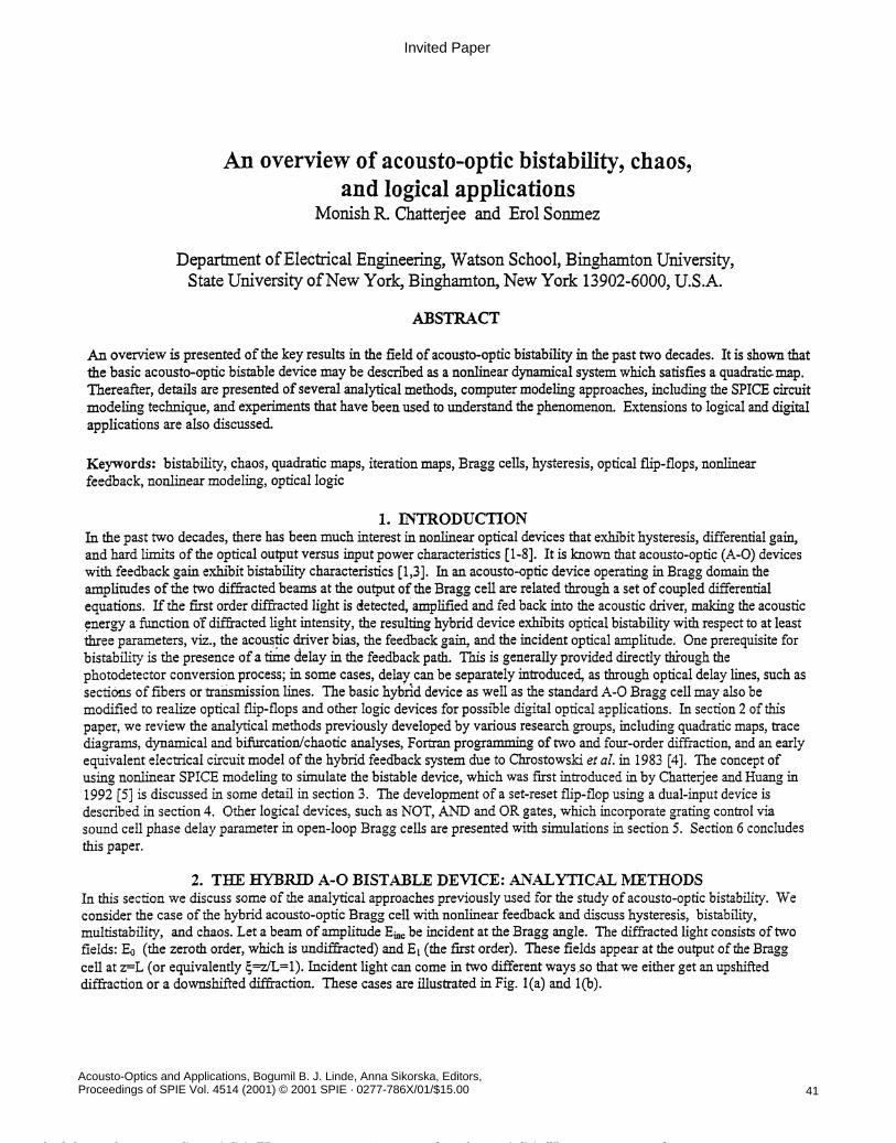
2. TIlE HYBRID A-O BISTABLE DEVICE: ANALYTICAL METHODSIn this section we discuss some of the analytical approaches previously used for the study of acousto-optic bistability. Weconsider the case ofthe hybrid acousto-optic Bragg cell with nonlinear feedback and discuss hysteresis, bistability,multistability, and chaos. Let a beam of amplitude be incident at the Bragg angle. The diffracted light consists of twofields: E0 (the zeroth order, which is undif&acted) and E1 (the first order). These fields appear at the output ofthe Braggcell at z=L (or equivalently =zfL=l). Incident light can come in two different ways so that we either get an upshifteddiffraction or a downshifted diffraction. These cases are illustrated in Fig. 1(a) and 1(b).
Acousto-Optics and Applications, Bogumil B. J. Linde, Anna Sikorska, Editors,Proceedings of SPIE Vol. 4514 (2001) © 2001 SPIE · 0277-786X/01/$15.00 41
Invited Paper
Downloaded From: http://proceedings.spiedigitallibrary.org/ on 07/21/2016 Terms of Use: http://spiedigitallibrary.org/ss/TermsOfUse.aspx
tK ___
() (b)
Fig. 1. Acousto-optic device operating . in the Bragg regime: (a) upshi.fted Bragg diffracon, (b) downshifted Braggdiffraction (after [5J).
To determine the diffracted outputs we use the well-known coupled differential equations for the two Bragg orders.Considering upshifted diffraction, the coupled differential equations for E0 and E1 within the Bragg cell are given (in termsof the normalized longitudinal distance (= ilL) where L is the so-called interaction width) by [9]
dE0 &—=—j—E1, (la)
=-jE0. (Th)
Equations (la) and (ib) are solved to give
(a"iE0(ç) = Acos + Bsni — , (2a)
E1()= CcosJ+Ds(). (2b)
With the initial conditions E0(O) = E1(O) = 0, the solutions for the field inside the Bragg cell may be obtained as
E0 () =E1, cos , (3a)
E1() = -jE1 sin (J . (3b)
At the output of the Bragg cell (z=l or =l) we have
Proc. SPIE Vol. 451442
Downloaded From: http://proceedings.spiedigitallibrary.org/ on 07/21/2016 Terms of Use: http://spiedigitallibrary.org/ss/TermsOfUse.aspx
(aE =E. Co
= -jLsin(IJ
,
The above fields may be expressed in intensity form as
21"a'\11=1inc t\2)
2(a)Io=Iinccos I—
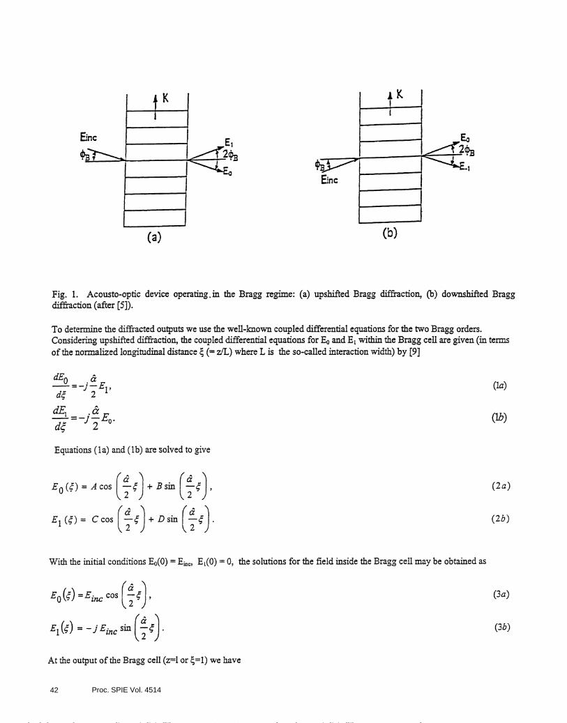
where '= I E0 2 11= E1 I2 ii= I E 12, and is the total phase delay.
Fig. 2. Hybrid bistable device (after [5]).
(3c)
(3d)
(4a)
(4b)
Fig. 2 shows a hybrid bistable device based on Bragg diffraction [1,2,8]. An incident field Eth at z=O generates two fieldsE0 andE at z=L. The first-order diffracted field E1 is detected and fed back into the generator making the acoustic energya function of the diffracted light intensity. Total phase delay a may be expressed as
a=ao+ f3IE1 12,
where 13 is the effective feedback gain, o is the external bias to the source driver.
(5)
Einc
Proc. SPIE Vol. 4514 43
Downloaded From: http://proceedings.spiedigitallibrary.org/ on 07/21/2016 Terms of Use: http://spiedigitallibrary.org/ss/TermsOfUse.aspx
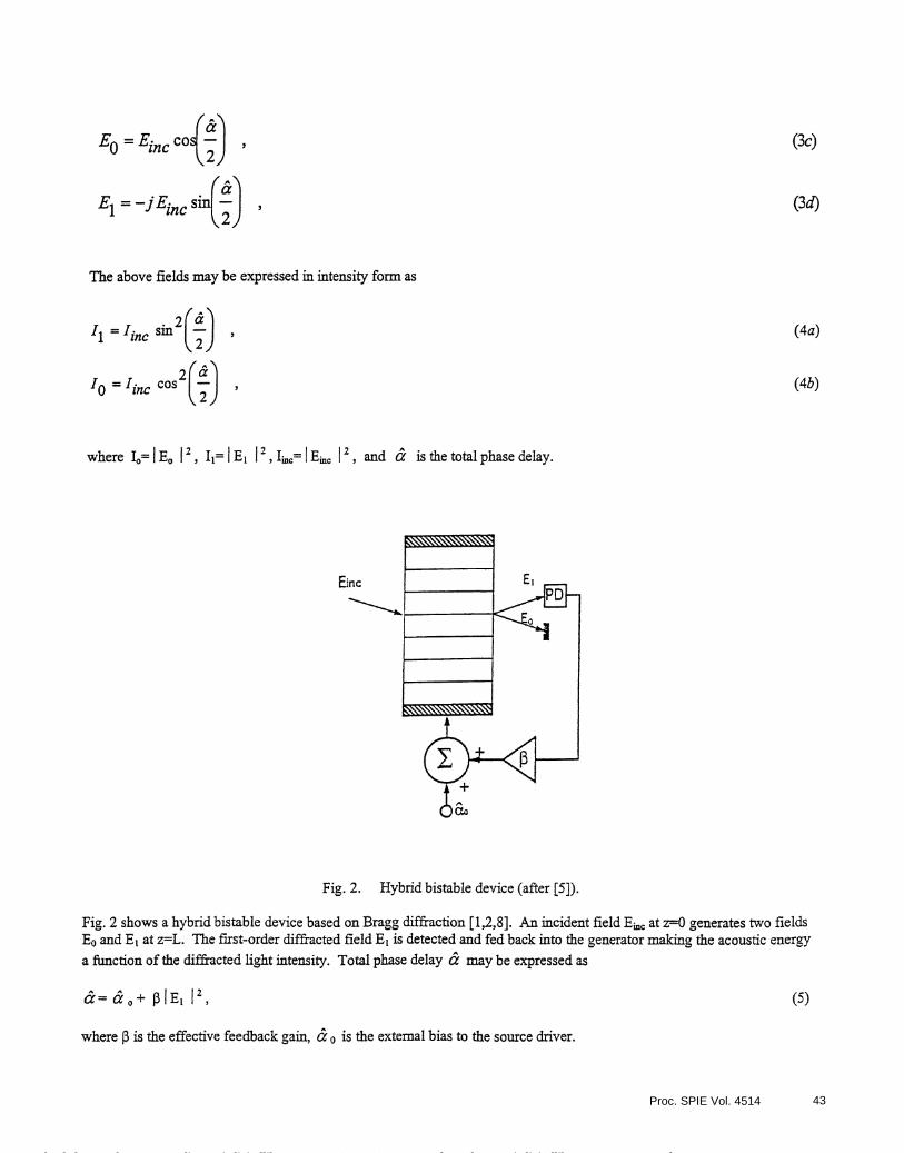
The steady state behavior ofthe device is given by the simultaneous solution ofEqs.(4a) and (5). Note that the intensity onthe LHS of Eq.(4), or the amplitude on the LHS of Eq.(3), recurs after a time delay suffered during feedback via the field-
dependent a parameter (Eq.(5)). This time delay is crucial to bistability and chaos in this dynamical system. Furtherdetails are presented in section that follows. There are three modes ofoperation each leading to a hysteresis curve for the
output intensity: (a) varying the input intensity, (b) varying the gain in the feedback path, and (c) varying the bias voltage
a0. Fig. 3 shows the graphical solutions of eqs.(la) and (5) for three modes of operation.
a0
a0- 0+
U
(c)(3) (b)
Fig. 3. Three modes ofoperation ofthe acousto-optic bistable device (after[l]): (a) input intensity tuning, (b) feedback gaintuning, (c) bias voltage tuning.
Fig. 3(a) shows the mode of operation leading to hysteretic behavior in the output versus input intensity curve. The
straight line starting from a = corresponds to the feedback loop. Changing the laser intensity from lower bistabilitylimit I_ to upper bistability limit 1+ one gets all the intermediate curves between I and 1+. Let the curve marked I
correspond to the initial laser intensity (Ii). The operating point o is chosen in such a way that the feedback line crossesthe curve I both in the lower part of the curve, i.e., the "off" state, from initial off state to on state, one has toincrease theinput laser intensity from I to 1+, for which only one solution offormulations (la) and (5)exists. When the input intensityis decreased, the system still stays in the on state until the feedback line is tangent to the transmission curve marked I_,where the system switches to the off state.
Fig. 3(b) describes the feedback tuning mode with the input intensity fixed. It is possible to switch from offto on and viceversa by chahging j3, where 3 is the inverse of the slope ofthe feedback line. The parameters f3+ and 3 are the maximumand minimum gains for bistability, respectively.
Fig. 3(c) shows the third mode of operation for a varying bias voltage o with the input intensity and gain fixed. The
values a . and a+ are the voltage limits within which bistability is obtained.
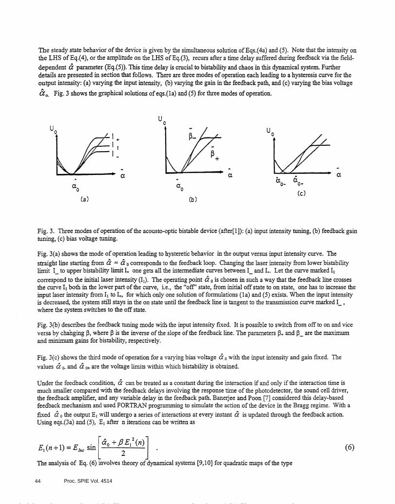
Under the feedback condition, a can be treated as a constant during the interaction if and only if the interaction time ismuch smaller compared with the feedback delays involving the response time of the photodetector, the sound cell driver,the feedback amplifier, and any variable delay in the feedback path. Banerjee and Poon [7] considered this delay-basedfeedback mechanism and used FORTRAN programming to simulate the action of the device in the Bragg regime. With a
fixed the output E1 will undergo a series of interactions at every instant a is updated through the feedback action.Using eqs.(3a) and (5), E1 after n iterations can be written as
E1(n+1)=E1+flE12(n)]
. (6)
The analysis of Eq. (6) involves theory of dynamical systems [9,1O for quadratic maps ofthe type
Proc. SPIE Vol. 451444
Downloaded From: http://proceedings.spiedigitallibrary.org/ on 07/21/2016 Terms of Use: http://spiedigitallibrary.org/ss/TermsOfUse.aspx
(7)
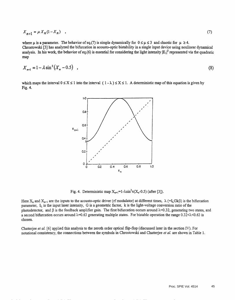
where JL iS a parameter. The behavior of eq.(7) is simple dynamically for 0 � j.t � 3 and chaotic for t � 4.Chrostowski [3] has analyzed the bifurcation in acousto-optic bistability in a single input device using nonlinear dynamicalanalysis. In his work, the behavior ofeq.(6) is essential for considering the light intensity JE1j2 represented via the quadratic
map
X1=1—2sin2(X--O.5)
which maps the interval 0 � X � 1 into the interval ( 1 - X ) �X � 1 . A deterministic map ofthis equation is given byFig. 4.
X4:1
Fig. 4. Deterministic map X+1=1-?sin2ic(X-O.5) (after [3]).
(8)
Here X and X+1 are the inputs to the acousto-optic driver (rfmodulator) at different times, 2 (=ILGk3) is the bifurcationparameter, 'L is the input laser intensity, G is a geometric factor, k is the light-voltage conversion ratio of thephotodetector, and J3 is the feedback amplifier gain. The first bifurcation occurs around X=O.32, generating two states, anda second bifurcation occurs around =O.63 generating multiple states. For bistable operation the range O.32<2<O.63 ischosen.
Chatterjee et al. [6] applied this analysis to the zeroth order optical flip-flop (discussed later in the section IV). Fornotational consistency, the connections between the symbols in Chrostowski and Chatterjee et al. are shown in Table 1.
xn
Proc. SPIE Vol. 4514 45
Downloaded From: http://proceedings.spiedigitallibrary.org/ on 07/21/2016 Terms of Use: http://spiedigitallibrary.org/ss/TermsOfUse.aspx
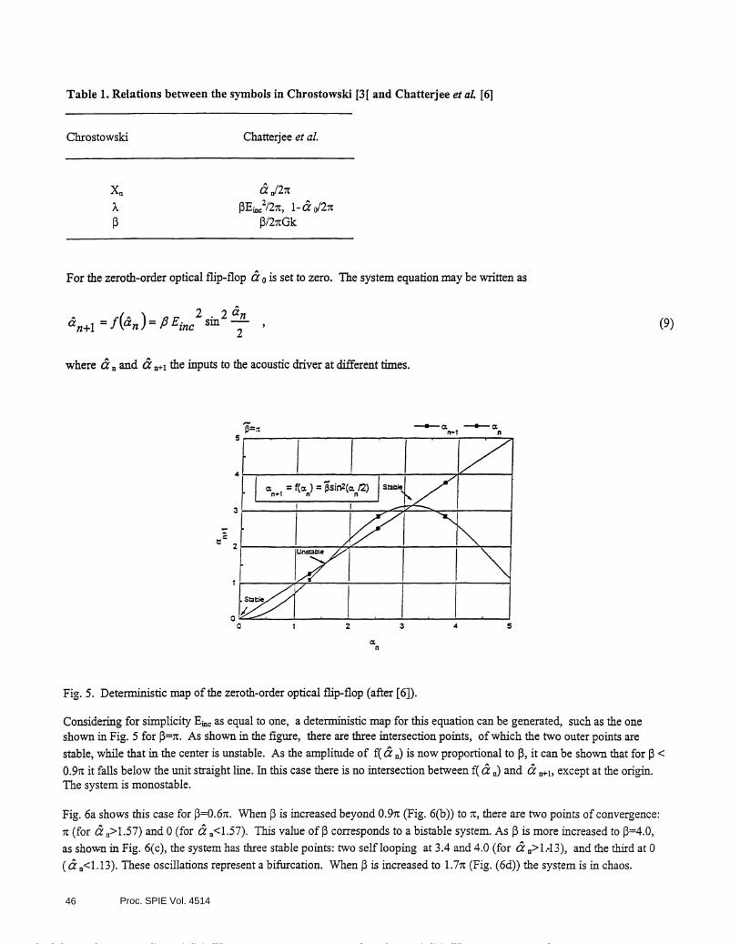
Table 1. Relations between the symbols in Chrostowski [3[ and Chatterjee et a!. [6j
Chrostowski Chatteijee et al.
xn a I2irx j3E2I2t, 1-&/2itJ3 f3/2itGk
For the zeroth-order optical flip-flop o is set to zero. The system equation may be written as
a1 jn) fiE12 2 nsm —2
where and n+1 the inputs to the acoustic driver at different times.
Fig. 5. Deterministic map ofthe zeroth-order optical flip-flop (after [6]).
(9)
Considering for simplicity Ej as equal to one, a deterministic map for this equation can be generated, such as the oneshown in Fig. 5 for f3=t. As shown in the figure, there are three intersection points, ofwhich the two outer points arestable, while that in the center is unstable. As the amplitude of f( a is now proportional to 3, it can be shown that for [3 <
O.9it it falls below the unit straight line. In this case there is no intersection between f( a and c except at the origin.The system is monostable.
Fig. 6a shows this case for f3=O.6n. When 3 is increased beyond O.9it (Fig. 6(b)) to it, there are two points of convergence:
IC (for a>l.57) and 0 (for a<l.57). This value of 3 corresponds to a bistable system. As 3 is more increased to J3=4.O,
as shown in Fig. 6(c), the system has three stable points: two seiflooping at 3.4 and 4.0 (for >ll3), and the third at 0
(a <i.i3). These oscillations represent a bifurcation. When is increased to 1 .7it (Fig. (6d)) the system is in chaos.
I,
Proc. SPIE Vol. 451446
Downloaded From: http://proceedings.spiedigitallibrary.org/ on 07/21/2016 Terms of Use: http://spiedigitallibrary.org/ss/TermsOfUse.aspx
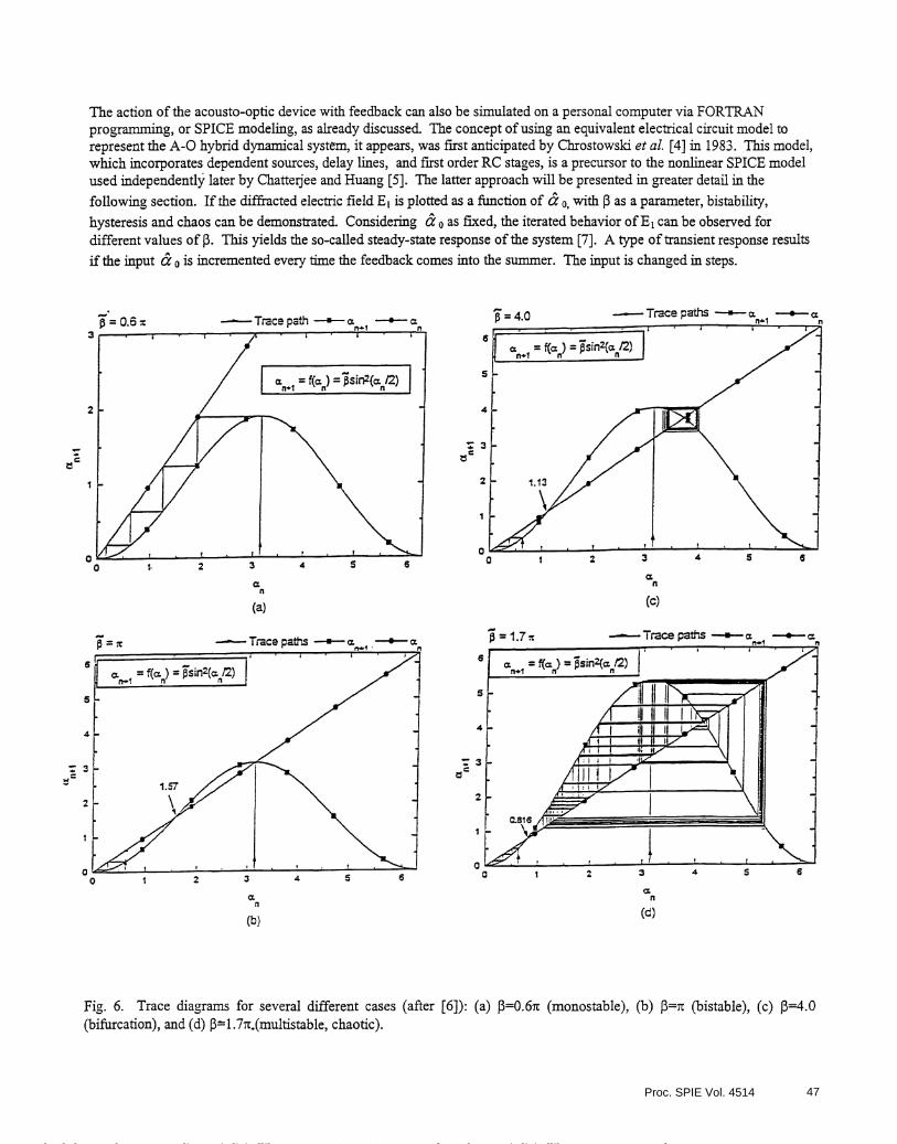
The action of the acousto-optic device with feedback can also be simulated on a personal computer via FORTRANprogramming, or SPICE modeling, as already discussed. The concept ofusing an equivalent electrical circuit model torepresent the A-O hybrid dynamical system, it appears, was first anticipated by Chrostowski et al. [4] in 1983. This model,which incorporates dependent sources, delay lines, and first order RC stages, is a precursor to the nonlinear SPICE modelused independently later by Chatterjee and Huang [5]. The latter approach will be presented in greater detail in thefollowing section. Ifthe diffracted electric field E1 is plotted as a function of o, with f3 as a parameter, bistabiity,hysteresis and chaos can be demonstrated. Considering o as fixed, the iterated behavior ofE1 can be observed fordifferent values of 3. This yields the so-called steady-state response ofthe system [7]. A type oftransient response resultsif the input incremented every time the feedback comes into the summer. The input is changed in steps.
Fig. 6. Trace diagrams for several different cases (after [6]): (a) f3=O.6it (monostable), (b) j3=rc (bistable), (c) f3=4.O(bifurcation), and (d) l .7it.(multistable, chaotic).
(a) (C)
3
(d)(b)
Proc. SPIE Vol. 4514 47
Downloaded From: http://proceedings.spiedigitallibrary.org/ on 07/21/2016 Terms of Use: http://spiedigitallibrary.org/ss/TermsOfUse.aspx
With the average rate of change being given by the ratio ofthe increment zS. a and the delay in the feedback. This change in
a related to an equivalent feedback delay (ta) through the following relationship,
(td H 2 (10)
t\ a0
where ta S the total sweep time ofthe input and o, is the peak value of a. Note that the & increment (ia in Eq. (8),which contributes to the feedback delay, is similar to the corresponding parameter in ref.[5]. Likewise, the delay tmentioned here reappears in the SPICE-based work by Chatterjee and co-workers [5,6]. Ifthe delay is ignored, the pointwhere the slope ofthe E1 versus & o curve becomes zero is at
aO(sat) = 7z — 1 (11)
In Banerjee and Poon [7], however, the time delay is not discussed explicitly.
3. TUE HYBRID A-O DEVICE: SPICE MODELINGIn this section we discuss nonlinear modeling ofthe hybrid A-O device. Each physical system can be modeled using acircuit modeL In many cases circuit models are simpler to understand and easier to test than other models. After developinga reasonably good circuit model, it becomes considerably more convenient to investigate the characteristics of the hybriddevice by means ofthe model. A circuit model that is appropriate for simulation that uses I-G SPICE package has beendeveloped by Chatterjee et al. [5,6]. Three types ofequivalent circuit models are used to demonstrate optical bistability,multistability, and chaos in these simulations.
Considering the interaction time in the device to be much smaller than the delay in the feedback path, acanbe treated asconstant during the interaction. Combining the eqs.(la) and (5) at =l (output ofthe acousto-optic device) we have
(a0 p 2'E1
=
sin1—--+ —E1
J(12)
This equation specifies the nature ofthe evolution ofE1 at the output. Because it was impossible to represent eq.(l2)entirely by a nonlinear SPICE model at that time, it is expanded in an infinite Taylor series
5 7
E1 ÷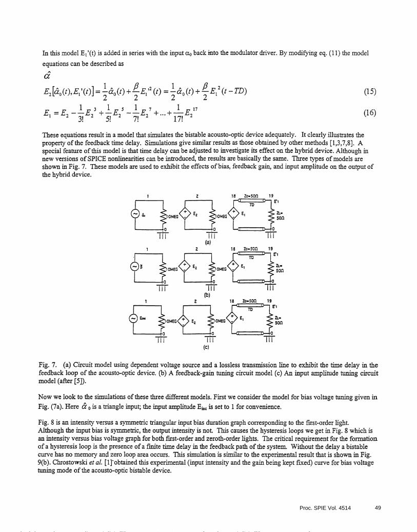
In this model E1 '(t) is added in series with the input back into the modulator driver. By modifying eq. (11) the model
equations can be described as
E[â0(t),'(t)]=a0(t)+E1?2(t) = Ia0(t)÷E12(t -TD)
E1 3! 2 5! 7! 2 17!
(15)
(16)
These equations result in a model that simulates the bistable acousto-optic device adequately. It clearly illustrates theproperty ofthe feedback time delay. Simulations give similar results as those obtained by other methods [1,3,7,8]. Aspecial feature ofthis model is that time delay can be adjusted to investigate its effect on the hybrid device. Although innew versions of SPICE nonlinearities can be introduced, the results are basically the same. Three types of models areshown in Fig. 7. These models are used to exhibit the effects ofbias, feedback gain, and input amplitude on the output ofthe hybrid device.
Ei
ZL.500
(C)
Fig. 7. (a) Circuit model using dependent voltage source and a lossless transmission line to exhibit the time delay in thefeedback loop of the acousto-optic device. (b) A feedback-gain tuning circuit model (c) An input amplitude tuning circuitmodel (after [5]).
Now we look to the simulations ofthese three different models. First we consider the model for bias voltage tuning given in
Fig. (7a). Here o is a triangle input; the input amplitude Ej is set to 1 for convenience.
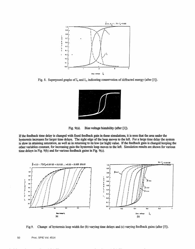
Fig. 8 is an intensity versus a symmetric triangular input bias duration graph corresponding to the first-order light.Although the input bias is symmetric, the output intensity is not. This causes the hysteresis loops we get in Fig. 8 which isan intensity versus bias voltage graph for both first-order and zeroth-order lights. The critical requirement for the formationof a hysteresis ioop is the presence ofa finite time delay in the feedback path ofthe system. Without the delay a bistablecurve has no memory and zero loop area occurs. This simulation is similar to the experimental result that is shown in Fig.9(b). Cbrostowski et a!. [l]obtained this experimental (input intensity and the gain being kept fixed) curve for bias voltagetuning mode ofthe acousto-optic bistable device.
Proc. SPIE Vol. 4514 49
Downloaded From: http://proceedings.spiedigitallibrary.org/ on 07/21/2016 Terms of Use: http://spiedigitallibrary.org/ss/TermsOfUse.aspx
N1•
EN$
1V
E O/ r0-o.o2!
—I 7
Iii eAtag. *
Fig. 8. Superposed graphs ofL and I, indicating conservation ofdiffracted energy (after [5]).
2.3 • : TDi%O.OO125 -.: 0.0125 ... :O.O2 — 0.025 0:0.05
Fig. 9(a). Bias voltage bistability (after [1}).
Tithe feedback time delay is changed with fixed feedback gain in these simulations, it is seen that the area under thehysteresis increases for larger time delays. The right edge ofthe loop moves to the left For a large time delay the systemis slow in attaining saturation, as well as in returning to its low (or high) value. Tithe feedback gain is changed keeping theother variables constant for increasing gain the hysteresis loop moves to the left. Simulation results are shown for varioustime delays in Fig. 9(b) and for various feedback gains in Fig. 9(c).
Ta -O.OOf2$
Na:e__3iaN voitags
(a) (b)
Fig.9. Change of hysteresis ioop width for (b) varying time delays and (c) varying feedback gains (after [5]).
a
Proc. SPIE Vol. 451450
Downloaded From: http://proceedings.spiedigitallibrary.org/ on 07/21/2016 Terms of Use: http://spiedigitallibrary.org/ss/TermsOfUse.aspx
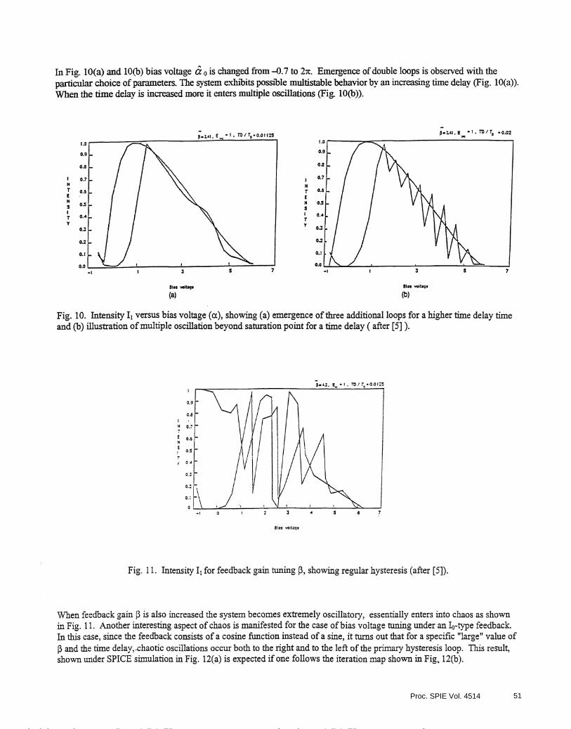
In Fig. 10(a) and 10(b) bias voltage o iS changed from —0.7 to 2t. Emergence ofdouble loops is observed with theparticular choice of parameters. The system exhibits possible multistable behavior by an increasing time delay (Fig. 1O(a).When the time delay is increased more it enters multiple oscillations (Fig. 10(b)).
Fig. 10. Intensity I versus bias voltage (a), showing (a) emergence ofthree additional loops for a higher time delay timeand (b) ifiustration ofmultiple oscillation beyond saturation point for a time delay (after [5]).
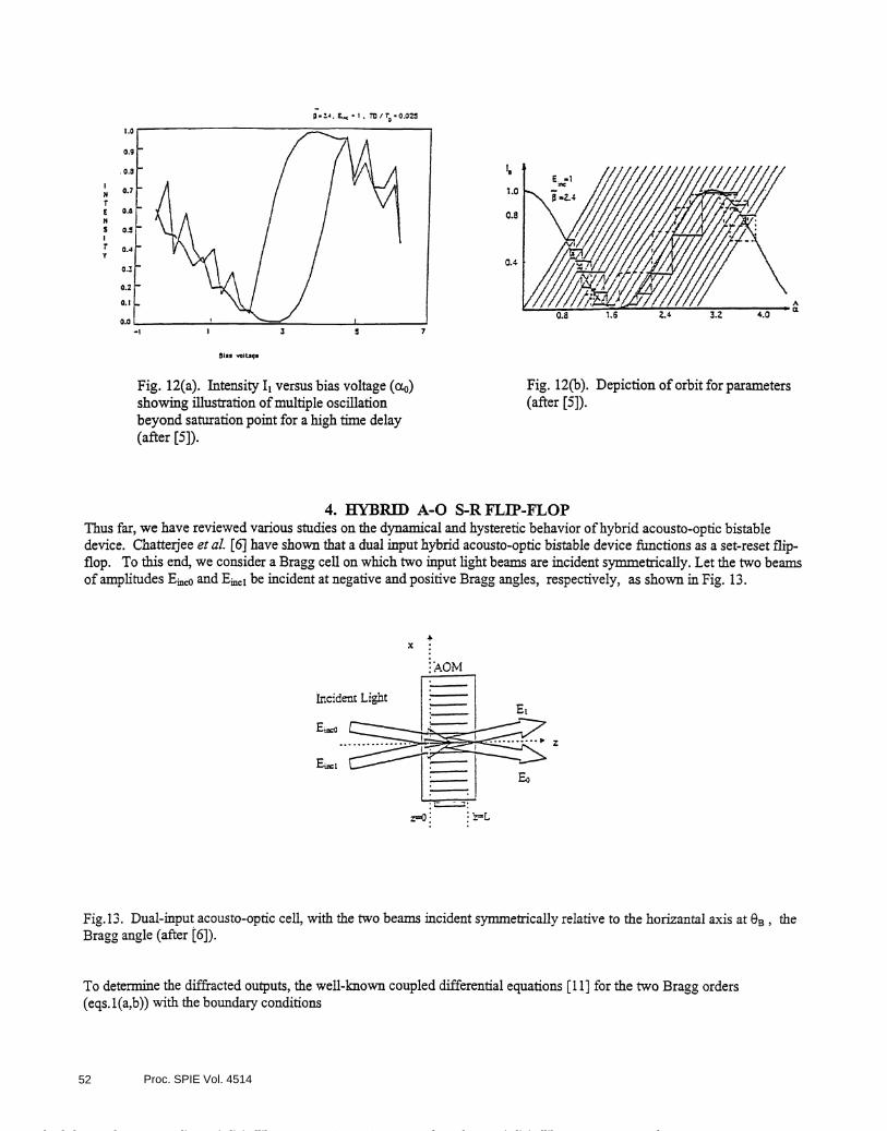
When feedback gain f3 is also increased the system becomes extremely oscillatory, essentially enters into chaos as shownin Fig. 11. Another interesting aspect of chaos is manifested for the case ofbias voltage tuning under an b-type feedback.In this case, since the feedback consists of a cosine function instead of a sine, it turns out that for a specific "large" value of
1 and the time delay,.chaotic oscillations occur both to the right and to the left ofthe primary hysteresis loop. This result,shown under SPICE simulation in Fig. 12(a) is expected if one follows the iteration map shown in Figs 12(b).
N1£NS
Y
Tot; —0.02
N1£N
rY
£t.s vsIbgi
(a)
£Iu voltage
(b)
Fig. 1 1 . Intensity I for feedback gain tuning 3, showing regular hysteresis (after [5]).
£iav valtaqe
Proc. SPIE Vol. 4514 51
Downloaded From: http://proceedings.spiedigitallibrary.org/ on 07/21/2016 Terms of Use: http://spiedigitallibrary.org/ss/TermsOfUse.aspx
N1
N
S
Y
P2.4. E,• TD/T-O.O2!
Fig. 12(a). Intensity I versus bias voltage (ao)showing ifiustration ofmultiple oscillationbeyond saturation point for a high time delay(after [5]).
Fig. 12(b). Depiction of orbit for parameters(after [5]).
4. HYBRID A-O S-R FLIP..FLOPThus far, we have reviewed various studies on the dynamical and hysteretic behavior ofhybrid acousto-optic bistabledevice. Chatterjee et aL [6] have shown that a dual input hybrid acousto-optic bistable device functions as a set-reset flip-flop. To this end, we consider a Bragg cell on which two input light beams are incident symmetrically. Let the two beamsof amplitudes Ej0 and E1 be incident at negative and positive Bragg angles, respectively, as shown in Fig. 13.
4x
AOM
z L
Fig.13. Dual-input acousto-optic cell, with the two beams incident symmetrically relative to the horizantal axis at eB the
Bragg angle (after [6]).
To determine the diffracted outputs, the well-known coupled differential equations [1 1] for the two Bragg orders(eqs.l(a,b)) with the boundary conditions
SIas vItg.
Incident Light
--...
Proc. SPIE Vol. 451452
Downloaded From: http://proceedings.spiedigitallibrary.org/ on 07/21/2016 Terms of Use: http://spiedigitallibrary.org/ss/TermsOfUse.aspx
E0(z = 0) = E1o,E1 (z = 0) =
for the E fields at z=0 must be solved. The solutions may be obtained as
= Eto cos — jE1i sin
E1 = E1i cos — jE1o sin (J.
These equations can be expressed in intensity form as
2('a10 = 'incO cos j-4) + 'md '
2('âIl = 'md cos + 'incO Sfl
(17)
(18)
(19)
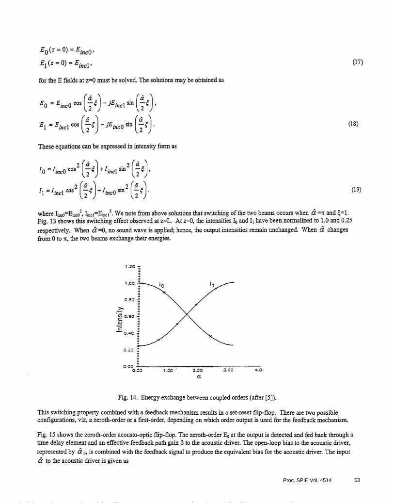
where I=E2, ImciEmci2. We note from above solutions that switching ofthe two beams occurs when a and =1.Fig. 13 shows this switching effect observed at z=L. At z=0, the intensities J and I have been normalized to 1.0 and 0.25
respectively. When â=0, no sound wave is applied; hence, the output intensities remain unchanged. When changesfrom 0 to it, the two beams exchange their energies.
0. C
Fig. 14. Energy exchange between coupled orders (after [5]).
This switching property combined with a feedback mechanism results in a set-reset flip-flop. There are two possibleconfigurations, viz, a zeroth-order or a first-order, depending on which order output is used for the feedback mechanism.
Fig. 15 shows the zeroth-order acousto-optic flip-flop. The zeroth-order E0 at the output is detected and fed back through atime delay element and an effective feedback path gain 13 to the acoustic driver. The open-loop bias to the acoustic driver,
represented by o, is combined with the feedback signal to produce the equivalent bias for the acoustic driver. The inputa to the acoustic driver is given as
1.cc
o.ac
c.5c
O.2C
Proc. SPIE Vol. 4514 53
Downloaded From: http://proceedings.spiedigitallibrary.org/ on 07/21/2016 Terms of Use: http://spiedigitallibrary.org/ss/TermsOfUse.aspx
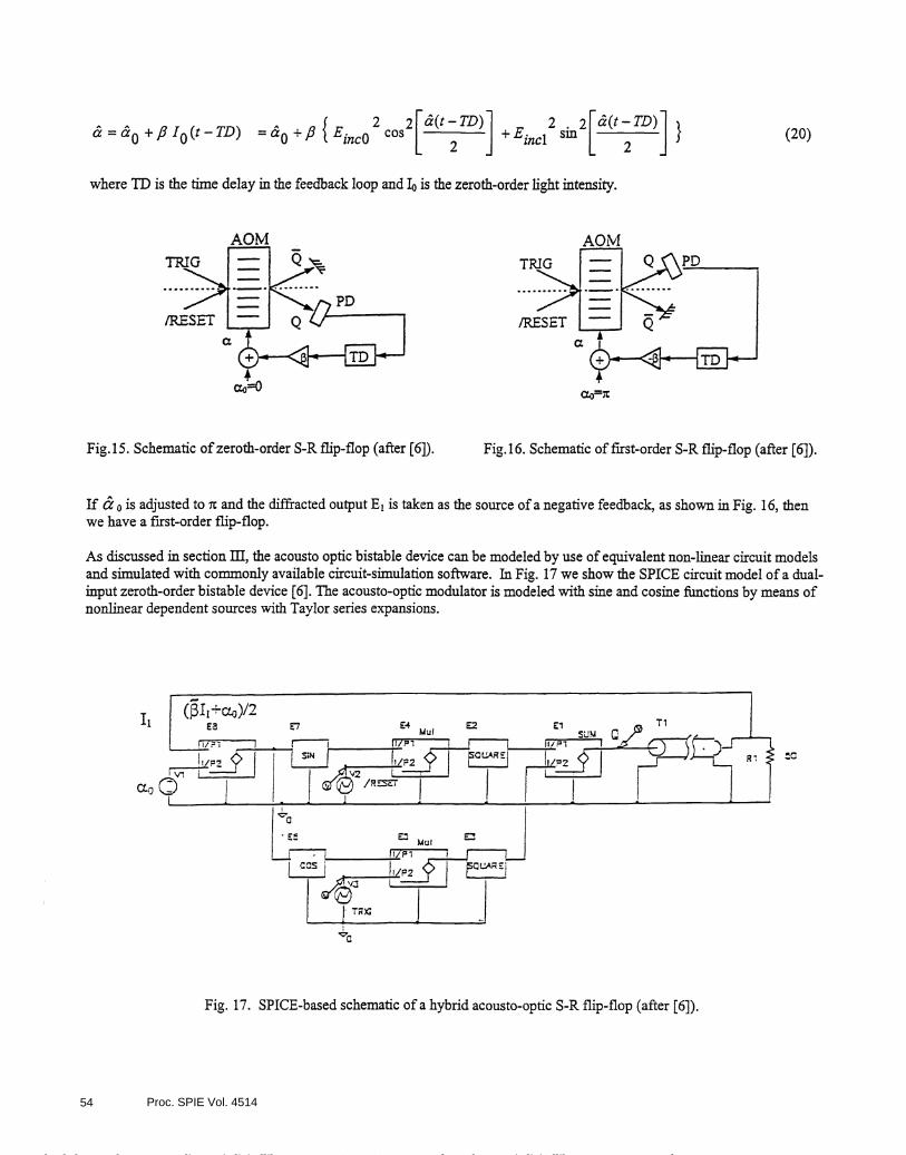
a = + fi 10(t —TD) = + fi { E02 cos2[t+
sin2[t —TD)]}
AOMP D
Fig.15. Schematic of zeroth-order S-R flip-flop (after [6]). Fig. 16. Schematic of first-order S-R flip-flop (after [6]).
I_f is adjusted to rc and the diffracted output E1 is taken as the source ofa negative feedback, as shown in Fig. 16, thenwe have a first-order flip-flop.
As discussed in section ifi, the acousto optic bistable device can be modeled by use of equivalent non-linear circuit modelsand simulated with commonly available circuit-simulation software. In Fig. 17 we show the SPICE circuit model ofa dual-input zeroth-order bistable device [6]. The acousto-optic modulator is modeled with sine and cosine fI.mctions by means ofnonlinear dependent sources with Taylor series expansions.
Ii
a0
Fig. 17. SPICE-based schematic ofa hybrid acousto-optic S-R flip-flop (after [6]).
where TD is the time delay in the feedback loop and I is the zeroth-order light intensity.
(20)
PD
a
Proc. SPIE Vol. 451454
Downloaded From: http://proceedings.spiedigitallibrary.org/ on 07/21/2016 Terms of Use: http://spiedigitallibrary.org/ss/TermsOfUse.aspx
The circuit time-.delay element is represented by a transmission line T1 with proper termination, and the photodetector issquaring-operator element that uses another nonlinear dependent source.
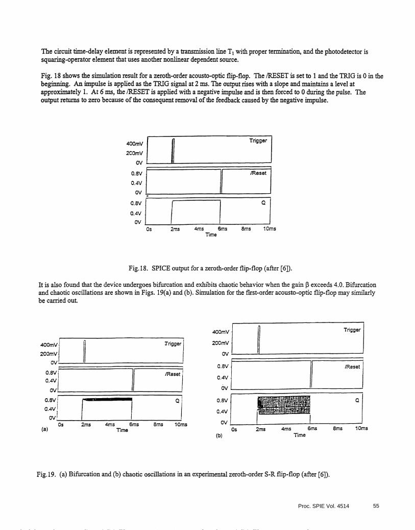
Fig. 18 shows the simulation result for a zeroth-order acousto-optic flip-flop. The IRESET is set to 1 and the TRIG is 0 in thebeginning. An impulse is applied as the TRIG signal at 2 ms. The output rises with a slope and maintains a level atapproximately 1. At 6 ins, the [RESET is applied with a negative impulse and is then forced to 0 during the pulse. Theoutput returns to zero because ofthe consequent removal ofthe feedback caused by the negative impulse.
400rnV
200rnV
cv-.
o.avjC.4V
ovLo.sv I
O.4V'
ov
400mV
2COmV
cv -o.8v
O.4V
ày
o.sv
O.4V
cv
11
Trigger400mV
2CCmV
cv
o.8v
O4V
cv
cayO.4v
cv
L
IT/Resj
QOs 2rris 4rriz 6r,s 8ms lOrns
Time
Fig.1 8. SPICE output for a zeroth-order flip-flop (after [6]).
It is also found that the device undergoes bifurcation and exhibits chaotic behavior when the gain f3 exceeds 4.0. Bifurcationand chaotic oscillations are shown in Figs. 19(a) and (b). Simulation for the first-order acousto-optic flip-flop may similarlybe carried out.
I
Trigger
Jr IReset
Trigger
TiOs 2rns 4ms 6ms Sms I Oms
(a) Time(b)
Fig.19. (a) Bifurcation and (b) chaotic oscillations in an experimental zeroth-order S-R flip-flop (after [6]).
Os 2ms 4ms 6ms 8msTime
lOms
Proc. SPIE Vol. 4514 55
Downloaded From: http://proceedings.spiedigitallibrary.org/ on 07/21/2016 Terms of Use: http://spiedigitallibrary.org/ss/TermsOfUse.aspx
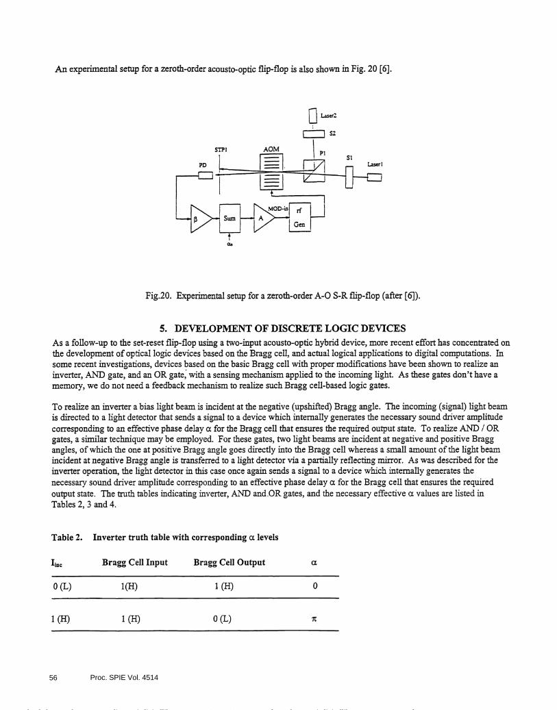
An experimental setup for a zeroth-order acousto-optic flip-flop is also shown in Fig. 20 [6].
Fig.20. Experimental setup for a zeroth-order A-O S-R flip-flop (after [6]).
5. DEVELOPMENT OF DISCRETE LOGIC DEVICESAs a follow-up to the set-reset flip-flop using a two-input acousto-optic hybrid device, more recent effort has concentrated onthe development of optical logic devices based on the Bragg cell, and actual logical applications to digital computations. Insome recent investigations, devices based on the basic Bragg cell with proper modifications have been shown to realize aninverter, AND gate, and an OR gate, with a sensing mechanism applied to the incoming light. As these gates don't have amemory, we do not need a feedback mechanism to realize such Bragg cell-based logic gates.
To realize an inverter a bias light beam is incident at the negative (upshifted) Bragg angle. The incoming (signal) light beamis directed to a light detector that sends a signal to a device which internally generates the necessary sound driver amplitudecorresponding to an effective phase delay a for the Bragg cell that ensures the required output state. To realize AND I ORgates, a similar technique may be employed. For these gates, two light beams are incident at negative and positive Braggangles, of which the one at positive Bragg angle goes directly into the Bragg cell whereas a small amount ofthe light beamincident at negative Bragg angle is transferred to a light detector via a partially reflecting mirror. As was described for theinverter operation, the light detector in this case once again sends a signal to a device which internally generates thenecessary sound driver amplitude corresponding to an effective phase delay c for the Bragg cell that ensures the requiredoutput state. The truth tables indicating inverter, AND andOR gates, and the necessary effective c values are listed inTables 2, 3 and 4.
Table 2. Inverter truth table with corresponding a levels
STP1
PD
S2
AOMSI
Lascrl
'inc Bragg Cell Input Bragg Cell Output a
0(L) 1(H) 1(H) 0
1(H) 1(H) 0(L) ir
Proc. SPIE Vol. 451456
Downloaded From: http://proceedings.spiedigitallibrary.org/ on 07/21/2016 Terms of Use: http://spiedigitallibrary.org/ss/TermsOfUse.aspx
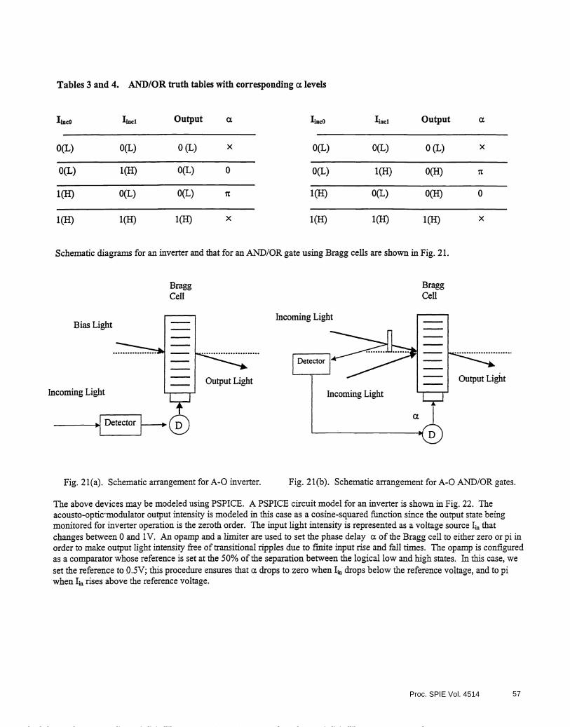
Tables 3 and 4. AND/OR truth tables with corresponding a levels
Schematic diagrams for an inverter and that for an AND/OR gate using Bragg cells are shown in Fig. 21.
BraggCell
BiasLight:_____LJ—
[Detector
BraggCell
Fig. 21(a). Schematic arrangement for A-O inverter. Fig. 21(b). Schematic arrangement for A-O AND/OR gates.
The above devices may be modeled using PSPICE. A PSPICE circuit model for an inverter is shown in Fig. 22. Theacousto-opticrnaodulator output intensity is modeled in this case as a cosine-squared function since the output state beingmonitored for inverter operation is the zeroth order. The input light intensity is represented as a voltage source I, thatchanges between 0 and 1V. An opamp and a limiter are used to set the phase delay a ofthe Bragg cell to either zero orpi inorder to make output light intensity free oftransitional ripples due to finite input rise and fall times. The opamp is configuredas a comparator whose reference is set at the 50% of the separation between the logical low and high states. In this case, weset the reference to Q.SV; this procedure ensures that a drops to zero when I drops below the reference voltage, and to piwhen I, rises above the reference voltage.
'incO 'mci Output a 'incO 'mci Output
0(L) 0(L) 0 (L) X
0(L) 1(H) 0(L) 0
1(H) 0(L) 0(L) it
a
1(H) 1(H 1(H
0(L) 0(L) 0 (L) X
0(L) 1(H) 0(H) it
1(H) 0(L) 0(H) 0
x 1(H) 1(H) 1(H) x
Incoming Light
Incoming Light
z...•..•....
Output LightLH::
Incoming Light
Output Light
Proc. SPIE Vol. 4514 57
Downloaded From: http://proceedings.spiedigitallibrary.org/ on 07/21/2016 Terms of Use: http://spiedigitallibrary.org/ss/TermsOfUse.aspx
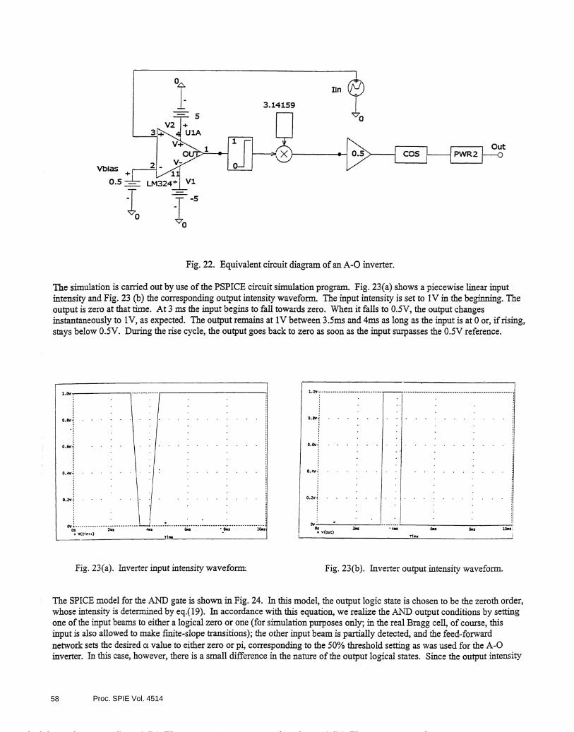
Vbias
0.5
Fig. 22. Equivalent circuit diagram of an A-O inverter.
The simulation is carried out by use ofthe PSPICE circuit simulation program. Fig. 23(a) shows a piecewise linear inputintensity and Fig. 23 (b) the corresponding output intensity waveform. The input intensity is set to IV in the beginning. Theoutput is zero at that time. At 3 ins the input begins to fall towards zero. When it falls to O.SV, the output changesinstantaneously to 1V, as expected. The output remains at 1V between 3.Sms and 4ms as long as the input is at 0 or, if rising,stays below O.5V. During the rise cycle, the output goes back to zero as soon as the input surpasses the O.5V reference.
1.Ov - -
o.3vi
O.6v
O.4V
0
:.. v(Out)
2 —.
Fig. 23(a). Inverter input intensity wavefornt Fig. 23(b). Inverter output intensity waveform.
The SPICE model for the AND gate is shown in Fig. 24. In this model, the output logic state is chosen to be the zerothorder,whose intensity is determined by eq.(19). In accordance with this equation, we realize the AND output conditions by settingone ofthe input beams to either a logical zero or one (for simulation purposes only; in the real Bragg cell, of course, thisinput is also allowed to make fmite-slope transitions); the other input beam is partially detected, and the feed-forwardnetwork sets the desired a value to either zero or pi, corresponding to the 50% threshold setting as was used for the A-Oinverter. In this case, however, there is a small difference in the nature ofthe output logical states. Since the output intensity
+1
Out
Proc. SPIE Vol. 451458
Downloaded From: http://proceedings.spiedigitallibrary.org/ on 07/21/2016 Terms of Use: http://spiedigitallibrary.org/ss/TermsOfUse.aspx
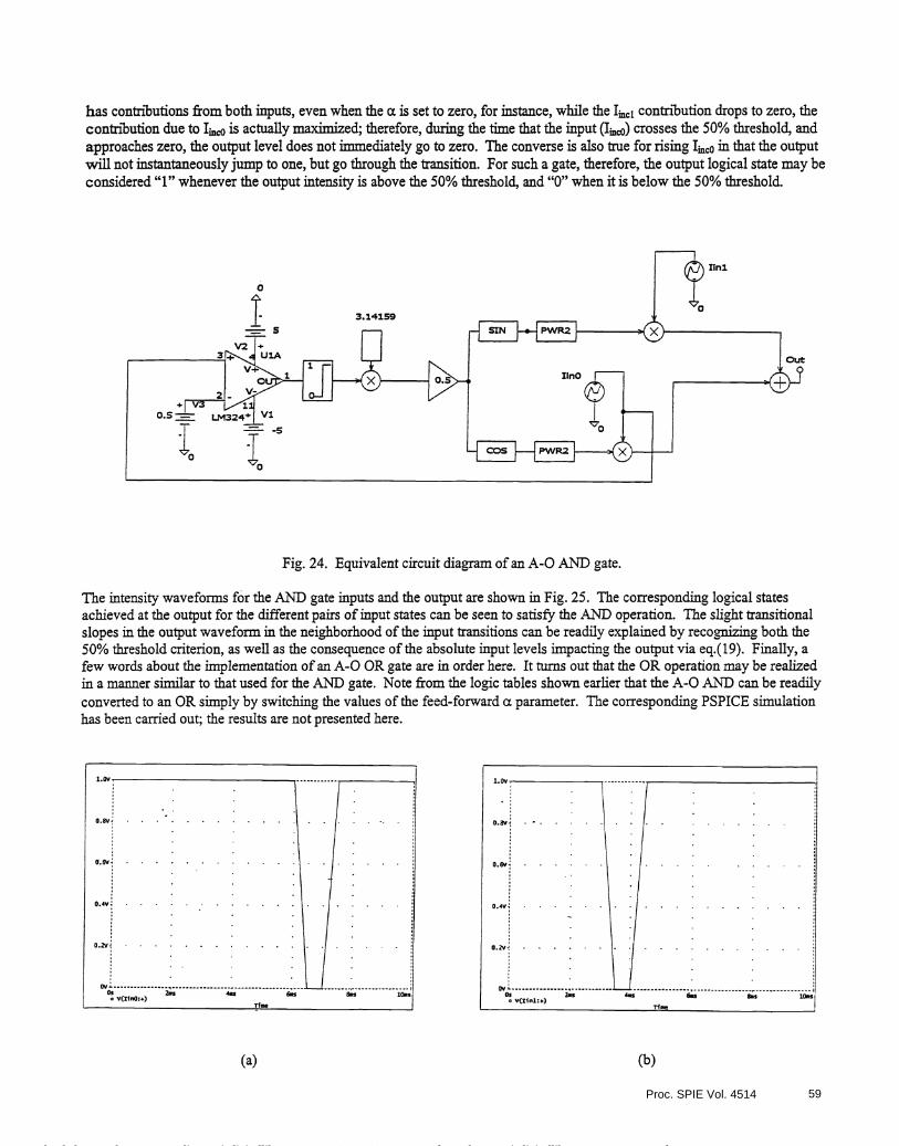
has contributions from both inputs, even when the a is set to zero, for instance, while the 'c1contribution drops to zero, thecontribution due to I is actually maximized; therefore, during the time that the input (I) crosses the 50%threshold, andapproaches zero, the output level does not immediately go to zero. The converse is also tme for rising 'jcO1 that the outputwill not instantaneously jump to one, but go through the iransition. For such a gate, therefore, the output logical state may beconsidered "1" whenever the output intensity is above the 50% threshold, and "0" when it is below the 50%threshold.
Fig. 24. Equivalent circuit diagram of an A-O AND gate.
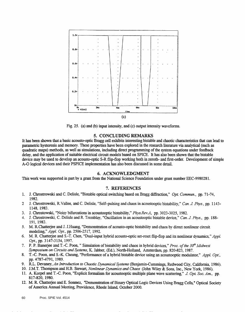
The intensity waveforms for the AND gate inputs and the output are shown in Fig. 25. The corresponding logical statesachieved at the output for the different pairs ofinput states can be seen to satisfy the AND operation. The slight transitionalslopes in the output waveform in the neighborhood of the input transitions can be readily explained by recognizing both the50% threshold criterion, as well as the consequence ofthe absolute input levels impacting the output via eq.(19). Finally, afew words about the implementation of an A-O OR gate are in order here. It turns out that the OR operation may be realizedin a manner similar to that used for the AND gate. Note from the logic tables shown earlier that the A-O AND can be readilyconverted to an OR simply by switching the values ofthe feed-forward a parameter. The corresponding PSPICE simulationhas been carried out; the results are not presented here.
(a) (b)
3.14159
Xml
Proc. SPIE Vol. 4514 59
Downloaded From: http://proceedings.spiedigitallibrary.org/ on 07/21/2016 Terms of Use: http://spiedigitallibrary.org/ss/TermsOfUse.aspx
5. CONCLUDING REMARKSIt has been shown that a basic acousto-optic Bragg cell exhibits interesting bistable and chaotic characteristics that can lead toparametric hysteresis and memory. These properties have been explored in the research literature via analytical (such asquadratic maps) methods, as well as simulations, including direct progziinming ofthe system equations under feedbackdelay, and the application of suitable electrical circuit models based on SPICE. It has also been shown that the bistabledevice may be used to develop an acousto-optic S-R flip-flop working both in zeroth- and first-order. Development of simpleA-O logical devices and their PSPICE implementation has also been discussed in some detail.
6. ACKNOWLEDGMENTThis work was supported in part by a grant from the National Science Founthtion under grant number EEC-9980281.
7. REFERENCES1. J. Chrostrowski and C. Delisle, "Bistable optical switching based on Bragg diffraction?' Opt. Commun., pp. 71-74,
1982.2 3. Chrostrowski, RVallee, and C. Delisle. "Self—pulsing and chaos in acoustooptic bistability," Can. J. Pkvs., pp. 1143-
1148, 1983.3. J. Chrostowski, "Noisy bifurcations in acoustooptic bistability," Pkvs.Rev.A, pp. 3023-3025, 1982.4. J. Chrostrowski, C. Delisle and R. Tremblay, "Oscillation in an acoustooptic bistable device," Can. J. Phvs., pp. 188-
191, 1983.5. M. RChatterjee and J. J.Huang, "Demonstration ofacousto-optic bistability and chaos by direct nonlinear circuit
modeling," Appi. Opt., pp. 2506-25 17, 1992.6. M. It Chatterjee and S.-T. Chen, "Dual-input hybrid acousto-optic set-reset ifip-flop and its nonlinear dynamics," Appi.
Opt., pp. 3147-3154, 1997.7. P. P. Banerjee and T.-C. Poon, " Simulation ofbistability and chaos in hybrid devices," Proc. ofthe 3O Midwest
Symposium on Circuits and Systems, K. Jabber, (Ed.), North-Holland, Amsterdam. pp. 820-823, 1987.8. T.-C. Poon, and S.-K. Cheung, "Performance ofa hybrid bistable device using an acoustooptic modulator," Appi. Opt.,
pp. 4787-4791, 1989.9. RL. Devaney, An Introduction to Chaotic Dynamical Systems (Benjaniin-Cuniniings, Redwood City, California. 1986).10. J.M.T. Thompson and RB. Stewart, Nonlinear Dynamics and Chaos (John Wiley & Sons, Inc., New York, 1986).I 1. A. Korpel and T.-C. Poon, "Explicit formalism for acoustooptic multiple plane wave scattering," J. Opt. Soc. Am., pp.
817-820, 1980.12. M. R. Chatterjee and E. Sonmez, "Demonstration ofBinaiy Optical Logic Devices Using Bragg Cells," Optical Society
ofAmerica Annual Meeting, Providence, Rhode Island. October 2000.
(c)
Fig. 25. (a) and (b) input intensity, and (c) output intensity waveforms.
Proc. SPIE Vol. 451460
Downloaded From: http://proceedings.spiedigitallibrary.org/ on 07/21/2016 Terms of Use: http://spiedigitallibrary.org/ss/TermsOfUse.aspx