Embed Size (px)
Citation preview
AS358/358A/358B Document number: DS36834 Rev. 6 - 2
1 of 19 www.diodes.com
May 2018 © Diodes Incorporated
AS358/358A/358B
LOW POWER DUAL OPERATIONAL AMPLIFIERS
Description
The AS358/358A/358B consists of two independent, high gain and
internally frequency compensated operational amplifiers, they are
specifically designed to operate from a single power supply.
Operation from split power supply is also possible and the low power
supply current drain is independent of the magnitude of the power
supply voltages. Typical applications include transducer amplifiers,
DC gain blocks and most conventional operational amplifier circuits.
The AS358/358A/358B series is compatible with industry standard
358. The AS358A has more stringent input offset voltage than the
AS358.
The AS358 is available in PDIP-8, TDIP-8, SO-8, TSSOP-8 and
MSOP-8 packages, the AS358A is available in PDIP-8 and SO-8
packages and AS358B is available in TSSOP-8 package.
Features
Internally Frequency Compensated for Unity Gain
Large Voltage Gain: 100dB (Typical)
Low Input Bias Current: 20nA (Typical)
Low Input Offset Voltage: 2mV (Typical)
Low Supply Current: 0.5mA (Typical)
Wide Power Supply Voltage:
Single Supply: 3V to 36V
Dual Supplies: ±1.5V to ±18V
Input Common Mode Voltage Range Includes Ground
Large Output Voltage Swing: 0V to VCC -1.5V
Lead-Free Packages: SO-8, PDIP-8 and TSSOP-8
Totally Lead-Free; RoHS Compliant (Notes 1 & 2)
Lead-Free Packages, Available in “Green” Molding Compound:
SO-8, PDIP-8, TDIP-8, TSSOP-8 and MSOP-8
Totally Lead-Free & Fully RoHS Compliant (Notes 1 & 2)
Halogen and Antimony Free. “Green” Device (Note 3)
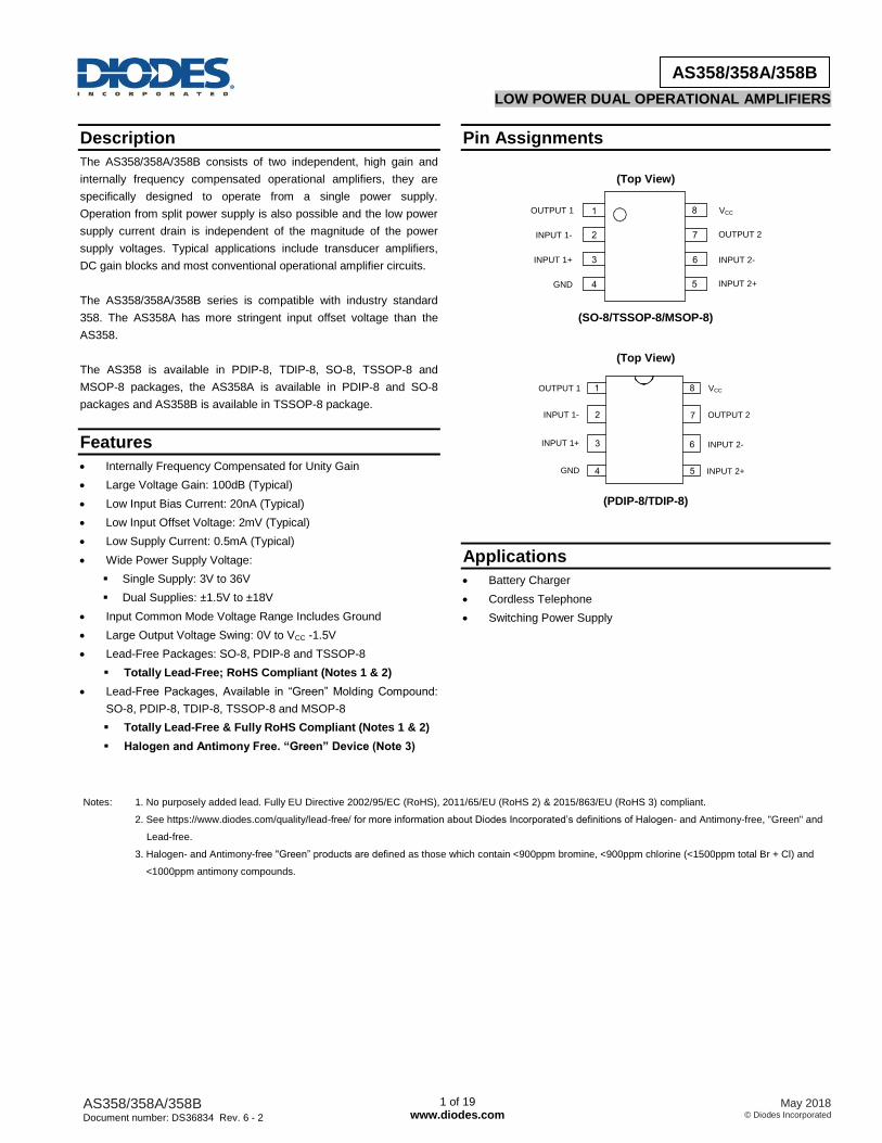
Pin Assignments
(Top View)
(SO-8/TSSOP-8/MSOP-8)
(Top View)
(PDIP-8/TDIP-8)
Applications
Battery Charger
Cordless Telephone
Switching Power Supply
Notes: 1. No purposely added lead. Fully EU Directive 2002/95/EC (RoHS), 2011/65/EU (RoHS 2) & 2015/863/EU (RoHS 3) compliant.
2. See https://www.diodes.com/quality/lead-free/ for more information about Diodes Incorporated’s definitions of Halogen- and Antimony-free, "Green" and
Lead-free.
3. Halogen- and Antimony-free "Green” products are defined as those which contain <900ppm bromine, <900ppm chlorine (<1500ppm total Br + Cl) and
<1000ppm antimony compounds.
1
2
3
4
8
7
6
5
INPUT 1-
INPUT 1+
OUTPUT 1 VCC
OUTPUT 2
INPUT 2-
INPUT 2+GND
INPUT 1-
INPUT 1+
OUTPUT 1 VCC
OUTPUT 2
INPUT 2-
INPUT 2+GND
1
2
3
4
8
7
6
5
AS358/358A/358B Document number: DS36834 Rev. 6 - 2
2 of 19 www.diodes.com
May 2018 © Diodes Incorporated
AS358/358A/358B
Typical Applications Circuit
AC
LineSMPS
R2Current
Sense
R7
R8
Battery
Pack
R4R3
AZ431
R5
R1
Opto
Isolator
VCC
GND
GND
1/2
AS358/A
+
-
1/2
AS358/A
R6
+
- VCC
Battery Charger
Power Amplifier DC Summing Amplifier
R1 910K
VO
R2 100K
R3 91K
VIN(+)
VCC
RL
1/2 AS358/A
-
+R6 100k
VOR5
100k
R1 100k
R2 100k
R3 100k
R4 100k
+V1
+V2
+V3
+V4
1/2 AS358/A
+
-
AS358/358A/358B Document number: DS36834 Rev. 6 - 2
3 of 19 www.diodes.com
May 2018 © Diodes Incorporated
AS358/358A/358B
Typical Applications Circuit (Cont.)
AC Coupled Non-Inverting Amplifier Fixed Current Sources
Pulse Generator DC Coupled Low-Pass Active Filter
R4 100k
VCC
R3
1M
R1 100k R2 1M
C1
0.1F
CIN
R5
100k
CO VO
1/2 AS358/A
RL
10k
C2
10FAV=1+R2/R1
AV=11 (As shown)
-
+
AC
RB6.2k
VCC
R4
3K
R3
2K
+
-
2V
+
-
2V
I1 I2
1mA
1/2 AS358/A
R1
2KR2
-
+
R5 100kR3 100k
R2 100k
R1 1M
VO
VCC
1/2 AS358/A
0.001F
-
+
R4
100k
VO
R2 16kR1 16K
VIN
R3
100k
1/2 AS358/A
R4
100k
C2
0.01F
C1 0.01F
fO
VO
0fO=1kHz
Q=1
AV=2
+
-
AS358/358A/358B Document number: DS36834 Rev. 6 - 2
4 of 19 www.diodes.com
May 2018 © Diodes Incorporated
AS358/358A/358B
Functional Block Diagram
Q2
Q4
Q3
Q1
Q8 Q9
6A 4A
Q10
Q11
50A
Q5
Q6
Q13
Rsc
Cc
100A
Q7
INPUTS
+
-
OUTPUT
Q12
VCC
Absolute Maximum Ratings (Notes 4 & 5)
Symbol Parameter Rating Unit
VCC Power Supply Voltage 40 V
VID Differential Input Voltage 40 V
VIC Input Voltage -0.3 to 40 V
PD Power Dissipation (TA = +25°C)
PDIP-8 830
mW
SO-8 550
TSSOP-8 500
MSOP-8 470
TJ Operating Junction Temperature +150 °C
TSTG Storage Temperature Range -65 to +150 °C
TLEAD Lead Temperature (Soldering, 10 Seconds) +260 °C
Notes: 4. Stresses greater than those listed under “Absolute Maximum Ratings” may cause permanent damage to the device. These are stress ratings only, and
functional operation of the device at these or any other conditions beyond those indicated under “Recommended Operating Conditions” is not implied.
Exposure to “Absolute Maximum Ratings” for extended periods may affect device reliability.
5. ESD sensitivity.
Recommended Operating Conditions
Symbol Parameter Min Max Unit
VCC Supply Voltage 3 36 V
TA Ambient Operating Temperature Range -40 +85 °C
AS358/358A/358B Document number: DS36834 Rev. 6 - 2
5 of 19 www.diodes.com
May 2018 © Diodes Incorporated
AS358/358A/358B
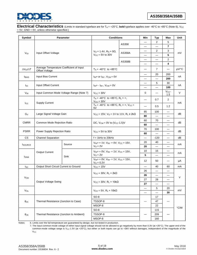
Electrical Characteristics (Limits in standard typeface are for TA = +25°C, bold typeface applies over -40°C to +85°C (Note 6), VCC
= 5V, GND = 0V, unless otherwise specified.)
Notes: 6. Limits over the full temperature are guaranteed by design, but not tested in production.
7. The input common-mode voltage of either input signal voltage should not be allowed to go negatively by more than 0.3V (at +25°C). The upper end of the
common-mode voltage range is VCC-1.5V (at +25°C), but either or both inputs can go to +36V without damages, independent of the magnitude of the
VCC。
Symbol Parameter Conditions Min Typ Max Unit
VIO Input Offset Voltage VO = 1.4V, RS = 0Ω,
VCC = 5V to 30V
AS358 — 2 5
mV
— — 7
AS358A — 2 3
— — 5
AS358B — — 2
— — 4
∆VIO/∆T Average Temperature Coefficient of Input Offset Voltage
TA = -40°C to +85°C — 7 — µV/°C
IBIAS Input Bias Current IIN+ or IIN-, VCM = 0V — 20 200
nA — — 200
IIO Input Offset Current IIN+ - IIN-, VCM = 0V — 5 30
nA — — 100
VIR Input Common Mode Voltage Range (Note 7) VCC = 30V 0 — VCC-1.5
V
ICC Supply Current
TA = -40°C to +85°C, RL = ∞,
VCC = 30V — 0.7 2
mA TA = -40°C to +85°C, RL = ∞, VCC = 5V
— 0.5 1.2
GV Large Signal Voltage Gain VCC = 15V, VO = 1V to 11V, RL ≥ 2kΩ 85 100 —
dB 80 — —
CMRR Common Mode Rejection Ratio DC, VCM = 0V to (VCC-1.5)V 60 70 —
dB 60 — —
PSRR Power Supply Rejection Ratio VCC = 5V to 30V 70 100 —
dB 60 — —
CS Channel Separation f = 1kHz to 20kHz — -120 — dB
ISOURCE
Output Current
Source VIN+ = 1V, VIN- = 0V, VCC = 15V,
VO = 2V
20 40 — mA
20 — —
ISINK Sink
VIN+ = 0V, VIN- = 1V, VCC = 15V,
VO = 2V
10 15 — mA
5 — —
VIN+ = 0V, VIN- = 1V, VCC = 15V,
VO = 0.2V 12 50 — µA
ISC Output Short Circuit Current to Ground VCC = 15V — 40 60 mA
VOH
Output Voltage Swing
VCC = 30V, RL = 2kΩ 26 — —
V 26 — —
VCC = 30V, RL = 10kΩ 27 28 —
27 — —
VOL VCC = 5V, RL = 10kΩ — 5 20
mV — — 30
θJC Thermal Resistance (Junction to Case)
SO-8
—
17
—
°C/W
TSSOP-8 47
MSOP-8 22
θJA Thermal Resistance (Junction to Ambient)
SO-8
—
115
— TSSOP-8 209
MSOP-8 160
AS358/358A/358B Document number: DS36834 Rev. 6 - 2
6 of 19 www.diodes.com
May 2018 © Diodes Incorporated
AS358/358A/358B
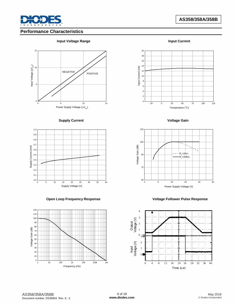
Input
Time (s)
Outp
ut
Vo
ltag
e (
V)
Vo
ltage
(V
)
0 4 8 12 16 20 24 28 32 36 40
0
1
2
3
1
2
3
4
0
Performance Characteristics
Input Voltage Range Input Current
Supply Current Voltage Gain
Open Loop Frequency Response Voltage Follower Pulse Response
0 5 10 150
5
10
15
POSITIVENEGATIVE
Inp
ut V
olta
ge
(+
VD
C)
Power Supply Voltage (+VDC
)
-25 0 25 50 75 100 1250
2
4
6
8
10
12
14
16
18
20
Inp
ut C
urr
en
t (n
A)
Temperature (oC)
0 5 10 15 20 25 30 35 400.0
0.1
0.2
0.3
0.4
0.5
0.6
0.7
0.8
0.9
1.0
Su
pp
ly C
urr
en
t (m
A)
Supply Voltage (V)
0 8 16 24 32 4060
75
90
105
120
Power Supply Voltage (V)
Vo
lta
ge
Ga
in (
dB
)
RL=2K
RL=20K
1 10 100 1k 10k 100k 1M0
10
20
30
40
50
60
70
80
90
100
110
120
Vo
lta
ge
Ga
in (
dB
)
Frequency (Hz)
AS358/358A/358B Document number: DS36834 Rev. 6 - 2
7 of 19 www.diodes.com
May 2018 © Diodes Incorporated
AS358/358A/358B
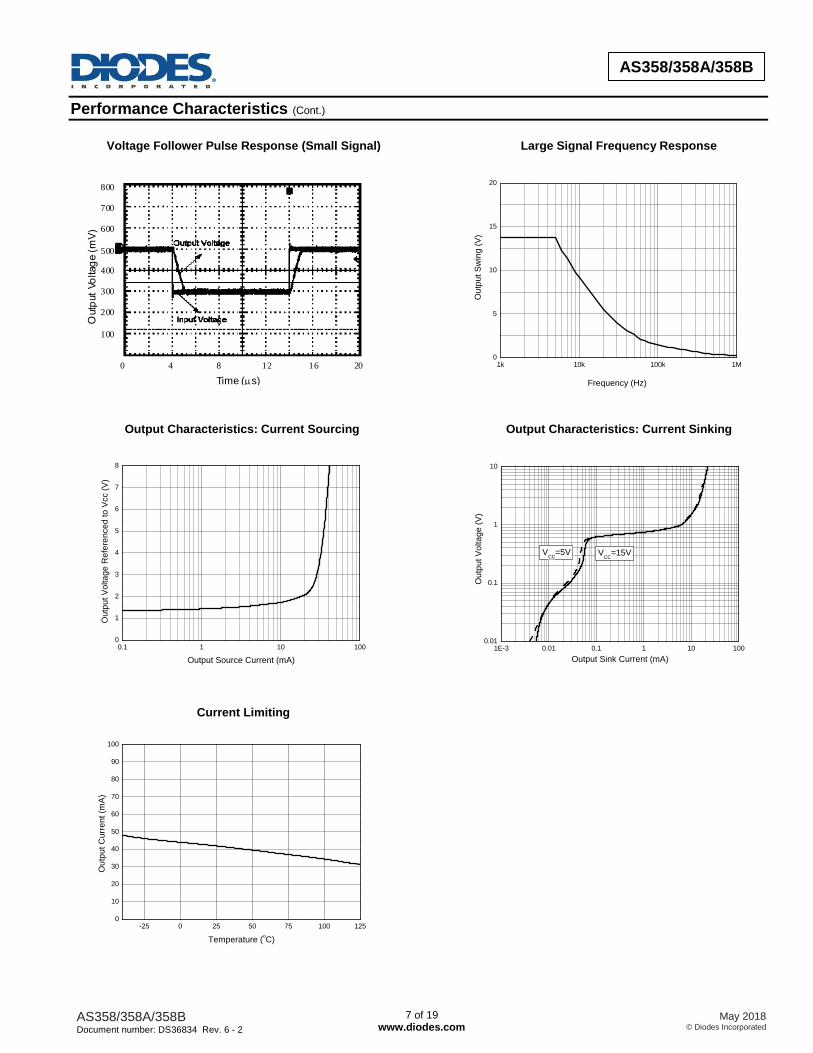
Time (s)
Outp
ut
Vo
ltag
e (
mV
)
0 4 8 12 16 20
100
200
300
400
500
600
700
800
Performance Characteristics (Cont.)
Voltage Follower Pulse Response (Small Signal) Large Signal Frequency Response
Output Characteristics: Current Sourcing Output Characteristics: Current Sinking
Current Limiting
1k 10k 100k 1M0
5
10
15
20
Frequency (Hz)
Ou
tpu
t S
win
g (
V)
0.1 1 10 1000
1
2
3
4
5
6
7
8
Ou
tpu
t V
olta
ge
Re
fere
nce
d to
Vcc (
V)
Output Source Current (mA)
1E-3 0.01 0.1 1 10 1000.01
0.1
1
10
VCC
=15V
Ou
tpu
t V
olta
ge
(V
)
Output Sink Current (mA)
VCC
=5V
-25 0 25 50 75 100 1250
10
20
30
40
50
60
70
80
90
100
Ou
tpu
t C
urr
en
t (m
A)
Temperature (oC)
AS358/358A/358B Document number: DS36834 Rev. 6 - 2
8 of 19 www.diodes.com
May 2018 © Diodes Incorporated
AS358/358A/358B
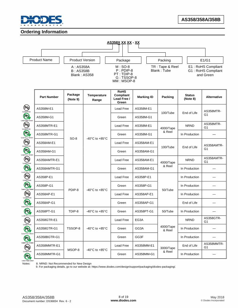
Ordering Information
AS358X XX XX - XX
PackingPackage
TR : Tape & ReelA : AS358A
Blank : AS358
Product Name
Blank : Tube
Product Version
G : TSSOP-8
M : SO-8P : PDIP-8
E1/G1
E1 : RoHS CompliantG1 : RoHS Compliant
and GreenPT : TDIP-8
MM : MSOP-8
B : AS358B
Part Number Package
(Note 9)
Temperature
Range
RoHS Compliant Lead Free /
Green
Marking ID Packing Status
(Note 8) Alternative
AS358M-E1
SO-8 -40°C to +85°C
Lead Free AS358M-E1 100/Tube End of Life
AS358MTR-G1 AS358M-G1 Green AS358M-G1
AS358MTR-E1 Lead Free AS358M-E1 4000/Tape
& Reel
NRND AS358MTR-G1
AS358MTR-G1 Green AS358M-G1 In Production —
AS358AM-E1 Lead Free AS358AM-E1 100/Tube End of Life AS358AMTR-
G1 AS358AM-G1 Green AS358AM-G1
AS358AMTR-E1 Lead Free AS358AM-E1 4000/Tape
& Reel
NRND AS358AMTR-G1
AS358AMTR-G1 Green AS358AM-G1 In Production —
AS358P-E1
PDIP-8 -40°C to +85°C
Lead Free AS358P-E1
50/Tube
In Production —
AS358P-G1 Green AS358P-G1 In Production —
AS358AP-E1 Lead Free AS358AP-E1 In Production —
AS358AP-G1 Green AS358AP-G1 End of Life —
AS358PT-G1 TDIP-8 -40°C to +85°C Green AS358PT-G1 50/Tube In Production —
AS358GTR-E1
TSSOP-8 -40°C to +85°C
Lead Free EG3A
4000/Tape & Reel
NRND AS358GTR-G1
AS358GTR-G1 Green GG3A In Production —
AS358BGTR-G1 Green GG3F In Production —
AS358MMTR-E1
MSOP-8 -40°C to +85°C Lead Free AS358MM-E1
3000/Tape & Reel
End of Life AS358MMTR-G1
AS358MMTR-G1 Green AS358MM-G1 In Production —
Notes: 8. NRND: Not Recommended for New Design
9. For packaging details, go to our website at: https://www.diodes.com/design/support/packaging/diodes-packaging/.
PbLead-Free
PbLead-Free
PbLead-Free
PbLead-Free
PbLead-Free
PbLead-Free
PbLead-Free
PbLead-Free
AS358/358A/358B Document number: DS36834 Rev. 6 - 2
9 of 19 www.diodes.com
May 2018 © Diodes Incorporated
AS358/358A/358B
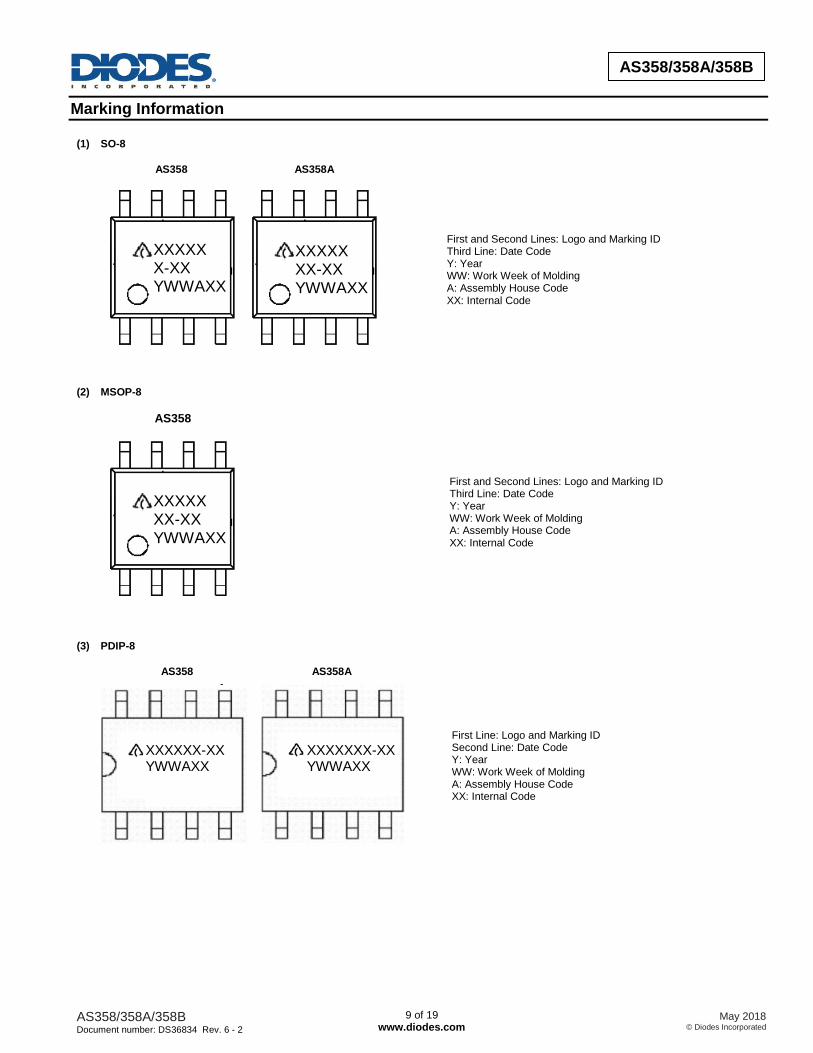
Marking Information
(1) SO-8
AS358 AS358A
(2) MSOP-8
AS358
(3) PDIP-8
AS358 AS358A
XXXXX X-XX YWWAXX
First and Second Lines: Logo and Marking ID Third Line: Date Code Y: Year WW: Work Week of Molding A: Assembly House Code XX: Internal Code
First Line: Logo and Marking ID Second Line: Date Code Y: Year WW: Work Week of Molding A: Assembly House Code XX: Internal Code
XXXXX XX-XX YWWAXX
XXXXX XX-XX YWWAXX
First and Second Lines: Logo and Marking ID Third Line: Date Code Y: Year WW: Work Week of Molding A: Assembly House Code XX: Internal Code
XXXXXX-XX YWWAXX
XXXXXXX-XX YWWAXX
AS358/358A/358B Document number: DS36834 Rev. 6 - 2
10 of 19 www.diodes.com
May 2018 © Diodes Incorporated
AS358/358A/358B
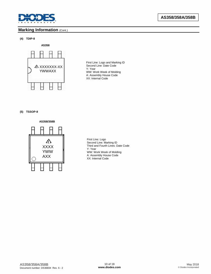
Marking Information (Cont.)
(4) TDIP-8
AS358
(5) TSSOP-8
AS358/358B
XXXX YWW AXX
First Line: Logo Second Line: Marking ID Third and Fourth Lines: Date Code Y: Year WW: Work Week of Molding A: Assembly House Code XX: Internal Code
First Line: Logo and Marking ID Second Line: Date Code Y: Year WW: Work Week of Molding A: Assembly House Code XX: Internal Code
XXXXXXX-XX YWWAXX
AS358/358A/358B Document number: DS36834 Rev. 6 - 2
11 of 19 www.diodes.com
May 2018 © Diodes Incorporated
AS358/358A/358B
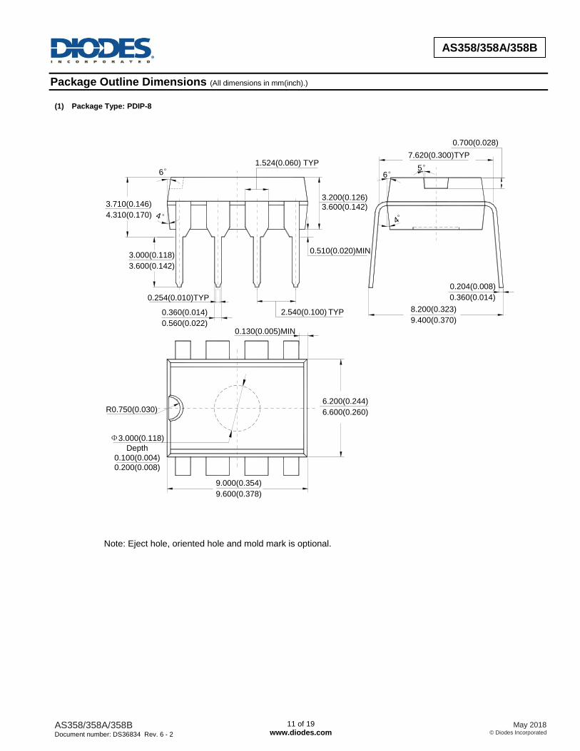
Package Outline Dimensions (All dimensions in mm(inch).)
(1) Package Type: PDIP-8
4°
6°
R0.750(0.030)
0.254(0.010)TYP
0.130(0.005)MIN
8.200(0.323)
9.400(0.370)
0.204(0.008)
0.360(0.014)
7.620(0.300)TYP
4°
6°5°
0.700(0.028)
9.000(0.354)
9.600(0.378)
3.710(0.146)
4.310(0.170)
3.000(0.118)
3.600(0.142)
0.360(0.014)
0.560(0.022)
2.540(0.100) TYP
6.200(0.244)
6.600(0.260)
3.200(0.126)
3.600(0.142)
0.510(0.020)MIN
Φ3.000(0.118)
Depth
0.100(0.004)
0.200(0.008)
1.524(0.060) TYP
Note: Eject hole, oriented hole and mold mark is optional.
AS358/358A/358B Document number: DS36834 Rev. 6 - 2
12 of 19 www.diodes.com
May 2018 © Diodes Incorporated
AS358/358A/358B
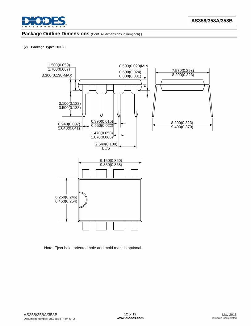
Package Outline Dimensions (Cont. All dimensions in mm(inch).)
(2) Package Type: TDIP-8
1.500(0.059)1.700(0.067)
3.300(0.130)MAX0.600(0.024)0.800(0.031)
0.940(0.037)1.040(0.041)
1.470(0.058)1.670(0.066)
2.540(0.100)BCS
3.100(0.122)3.500(0.138)
7.570(0.298)8.200(0.323)
8.200(0.323)9.400(0.370)
9.150(0.360)9.350(0.368)
6.250(0.246)6.450(0.254)
0.500(0.020)MIN
0.390(0.015)0.550(0.022)
Note: Eject hole, oriented hole and mold mark is optional.
AS358/358A/358B Document number: DS36834 Rev. 6 - 2
13 of 19 www.diodes.com
May 2018 © Diodes Incorporated
AS358/358A/358B
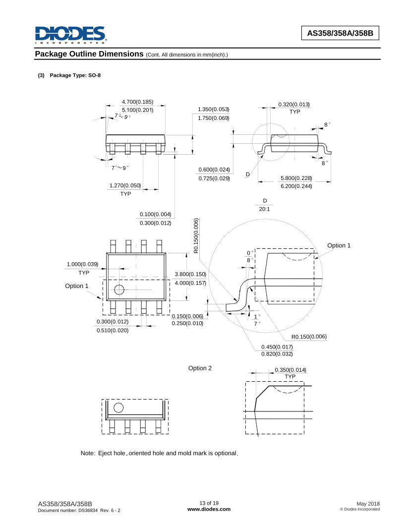
Package Outline Dimensions (Cont. All dimensions in mm(inch).)
(3) Package Type: SO-8
0°
8°
1°
7°
R0.150(0.006)
R0.1
50(0
.006)
1.000(0.039)
0.300(0.012)
0.510(0.020)
1.350(0.053)
1.750(0.069)
0.100(0.004)
0.300(0.012)
3.800(0.150)
4.000(0.157)
7°
7°
20:1
D
1.270(0.050)
TYP
0.150(0.006)
0.250(0.010)
8°
D5.800(0.228)
6.200(0.244)
0.600(0.024)
0.725(0.029)
0.320(0.013)
8°
0.450(0.017)
0.820(0.032)
4.700(0.185)
5.100(0.201)
Note: Eject hole , oriented hole and mold mark is optional.
Option 1
Option 1
Option 2 0.350(0.014)
TYP
TYP
TYP9°~
9°~
AS358/358A/358B Document number: DS36834 Rev. 6 - 2
14 of 19 www.diodes.com
May 2018 © Diodes Incorporated
AS358/358A/358B
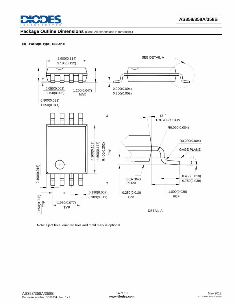
Package Outline Dimensions (Cont. All dimensions in mm(inch).)
(4) Package Type: TSSOP-8
4.3
00(0
.16
9)
0.4
00
(0.0
16
)
0.190(0.007)
0.300(0.012)
SEE DETAIL A
DETAIL A
2.900(0.114)
0.050(0.002)
0.150(0.006)1.200(0.047)
MAX
1.950(0.077)
0°
8°
12 °
TOP & BOTTOM
R0.090(0.004)
0.450(0.018)
0.750(0.030)
1.000(0.039)
6.4
00
(0.2
52
)0.800(0.031)
1.050(0.041)
0.090(0.004)
0.200(0.008)
GAGE PLANE
SEATINGPLANE
0.250(0.010)
3.100(0.122)
4.5
00(0
.17
7)
TY
P
0.6
50
(0.0
26
)
TY
P
TYP
TYP
R0.090(0.004)
REF
Note: Eject hole, oriented hole and mold mark is optional.
AS358/358A/358B Document number: DS36834 Rev. 6 - 2
15 of 19 www.diodes.com
May 2018 © Diodes Incorporated
AS358/358A/358B
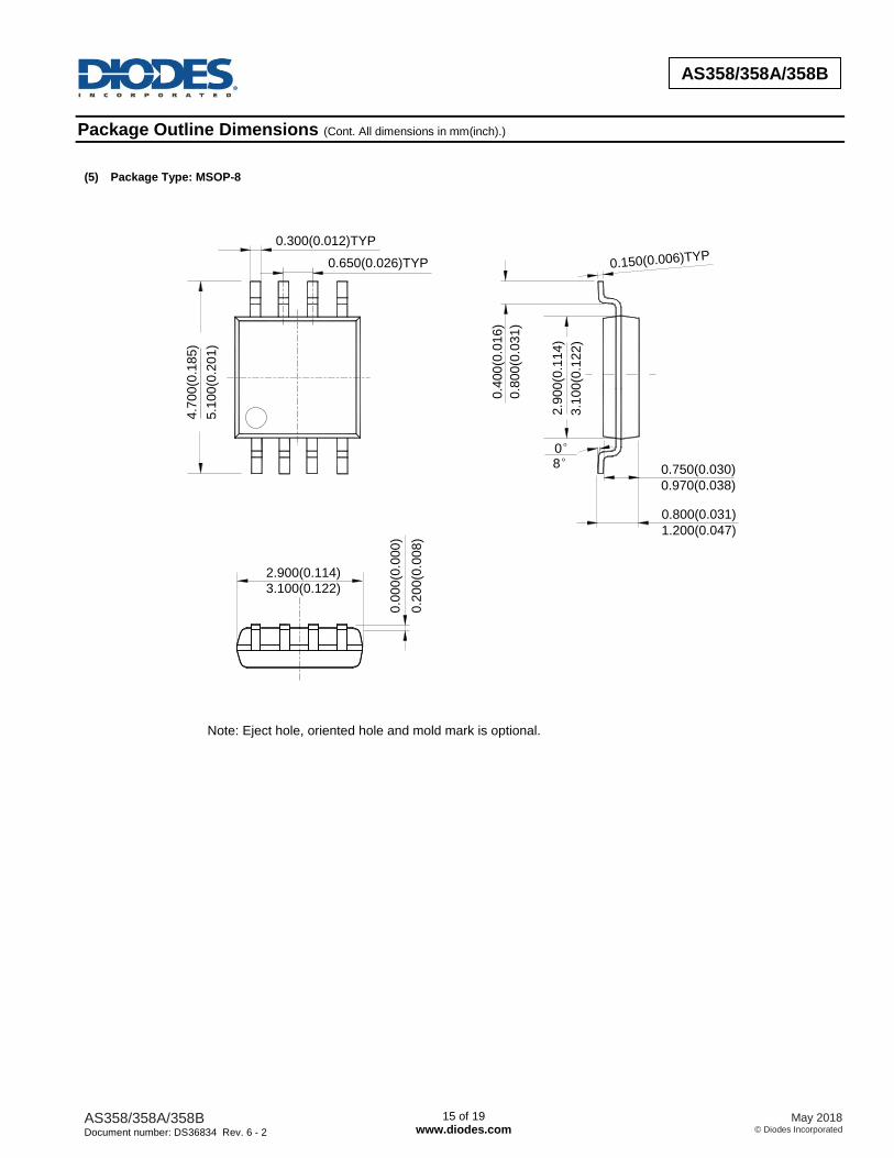
Package Outline Dimensions (Cont. All dimensions in mm(inch).)
(5) Package Type: MSOP-8
4.7
00
(0.1
85
)
0.650(0.026)TYP
5.1
00
(0.2
01
)
0.4
00
(0.0
16
)
0.8
00
(0.0
31
)
0.0
00(0
.00
0)
0. 2
00
(0.0
08)
0.300(0.012)TYP
3.1
00
(0.1
22
)
2. 9
00
(0.1
14
)
0.800(0.031)
1.200(0.047)
3.100(0.122)
2.900(0.114)
0°8°
0.150(0.006)TYP
0.750(0.030)
0.970(0.038)
`
Note: Eject hole, oriented hole and mold mark is optional.
AS358/358A/358B Document number: DS36834 Rev. 6 - 2
16 of 19 www.diodes.com
May 2018 © Diodes Incorporated
AS358/358A/358B
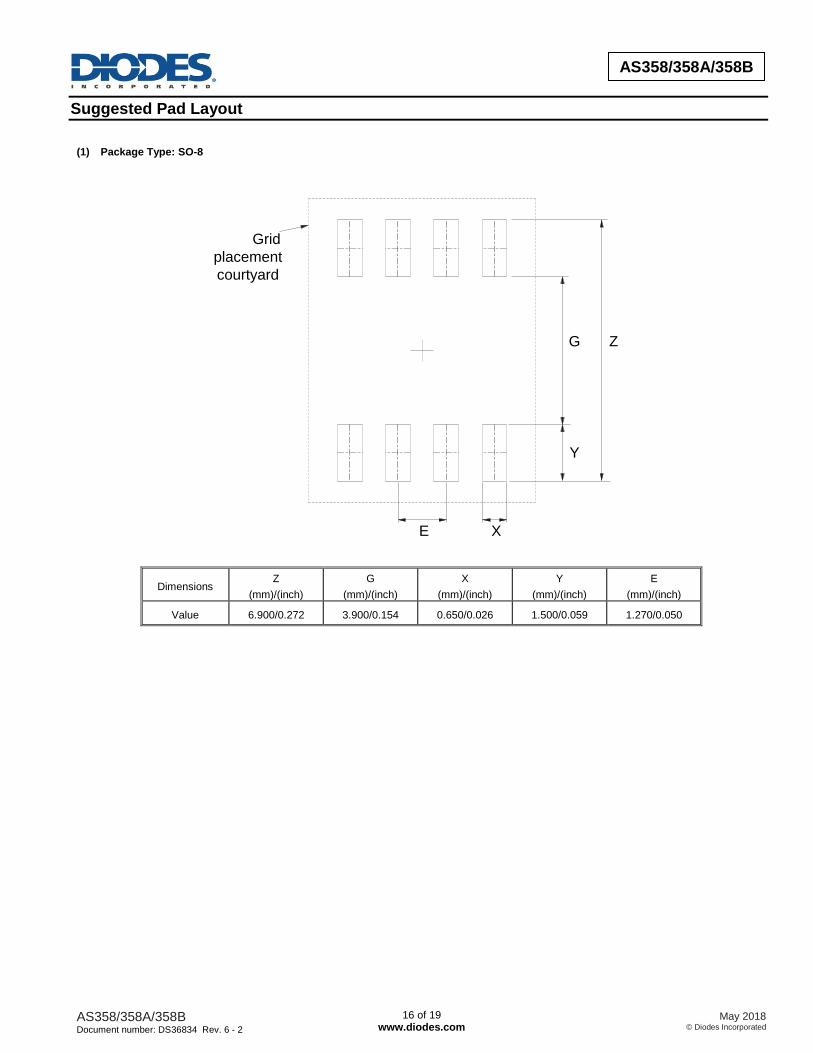
Suggested Pad Layout
(1) Package Type: SO-8
Grid
placement
courtyard
ZG
Y
E X
Dimensions Z
(mm)/(inch)
G
(mm)/(inch)
X
(mm)/(inch)
Y
(mm)/(inch)
E
(mm)/(inch)
Value 6.900/0.272 3.900/0.154 0.650/0.026 1.500/0.059 1.270/0.050
AS358/358A/358B Document number: DS36834 Rev. 6 - 2
17 of 19 www.diodes.com
May 2018 © Diodes Incorporated
AS358/358A/358B
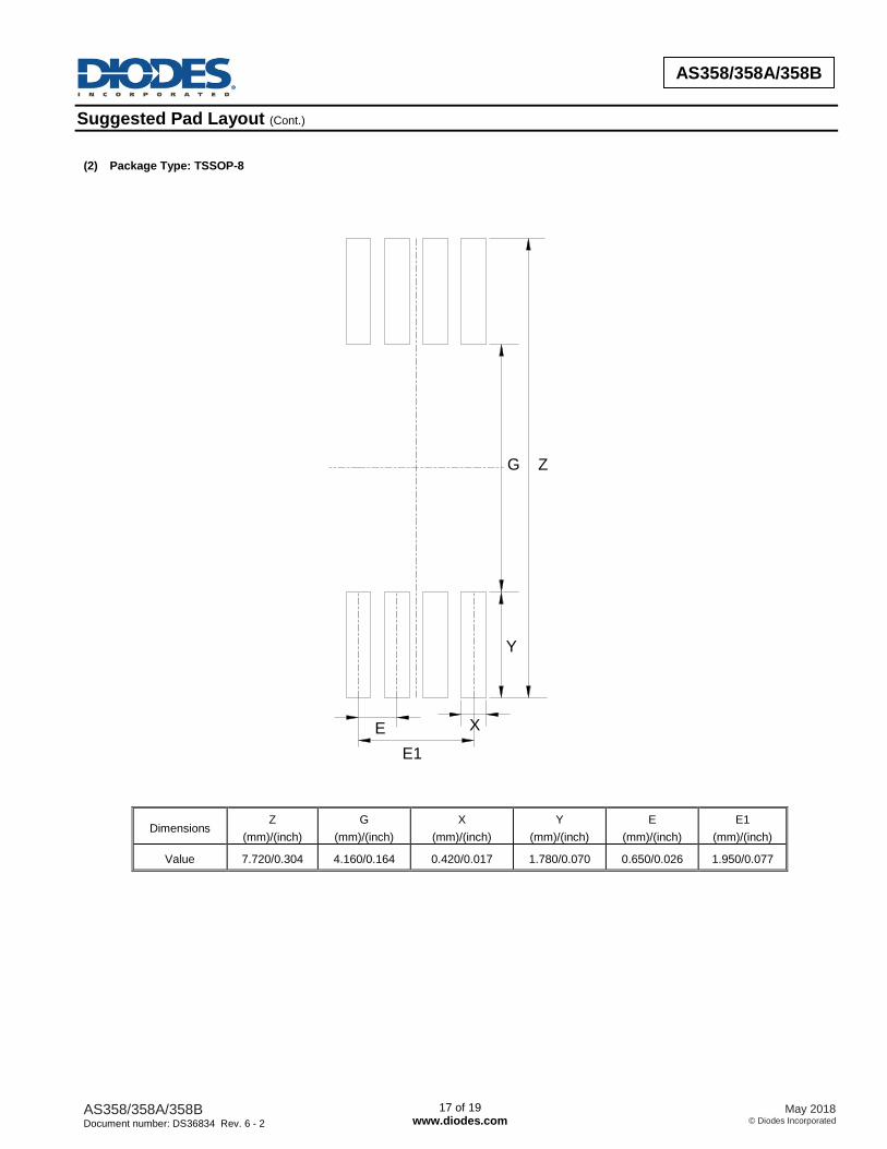
Suggested Pad Layout (Cont.)
(2) Package Type: TSSOP-8
Y
G Z
E1
E X
Dimensions Z
(mm)/(inch)
G
(mm)/(inch)
X
(mm)/(inch)
Y
(mm)/(inch)
E
(mm)/(inch)
E1
(mm)/(inch)
Value 7.720/0.304 4.160/0.164 0.420/0.017 1.780/0.070 0.650/0.026 1.950/0.077
AS358/358A/358B Document number: DS36834 Rev. 6 - 2
18 of 19 www.diodes.com
May 2018 © Diodes Incorporated
AS358/358A/358B
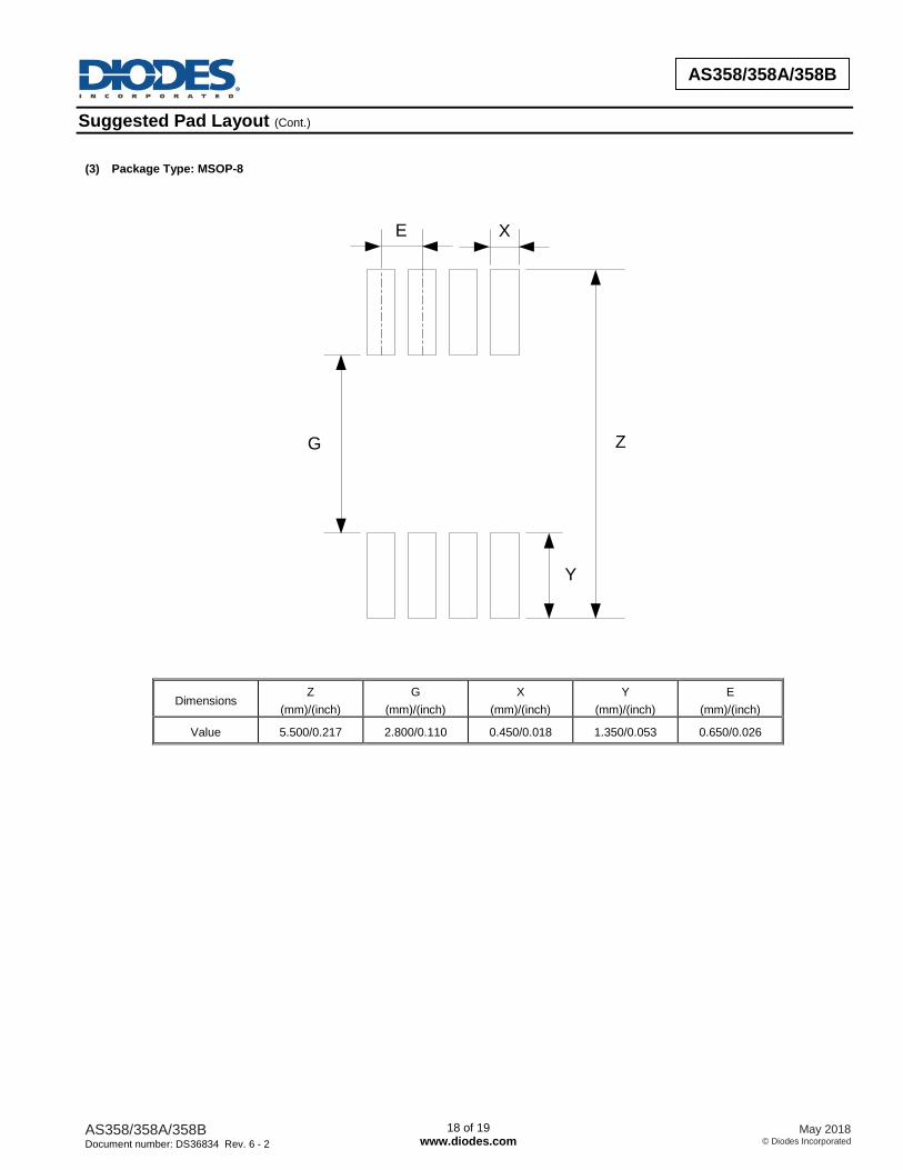
Suggested Pad Layout (Cont.)
(3) Package Type: MSOP-8
XE
Y
G Z
Dimensions Z
(mm)/(inch)
G
(mm)/(inch)
X
(mm)/(inch)
Y
(mm)/(inch)
E
(mm)/(inch)
Value 5.500/0.217 2.800/0.110 0.450/0.018 1.350/0.053 0.650/0.026
AS358/358A/358B Document number: DS36834 Rev. 6 - 2
19 of 19 www.diodes.com
May 2018 © Diodes Incorporated
AS358/358A/358B
IMPORTANT NOTICE DIODES INCORPORATED MAKES NO WARRANTY OF ANY KIND, EXPRESS OR IMPLIED, WITH REGARDS TO THIS DOCUMENT, INCLUDING, BUT NOT LIMITED TO, THE IMPLIED WARRANTIES OF MERCHANTABILITY AND FITNESS FOR A PARTICULAR PURPOSE (AND THEIR EQUIVALENTS UNDER THE LAWS OF ANY JURISDICTION). Diodes Incorporated and its subsidiaries reserve the right to make modifications, enhancements, improvements, corrections or other changes without further notice to this document and any product described herein. Diodes Incorporated does not assume any liability arising out of the application or use of this document or any product described herein; neither does Diodes Incorporated convey any license under its patent or trademark rights, nor the rights of others. Any Customer or user of this document or products described herein in such applications shall assume all risks of such use and will agree to hold Diodes Incorporated and all the companies whose products are represented on Diodes Incorporated website, harmless against all damages. Diodes Incorporated does not warrant or accept any liability whatsoever in respect of any products purchased through unauthorized sales channel. Should Customers purchase or use Diodes Incorporated products for any unintended or unauthorized application, Customers shall indemnify and hold Diodes Incorporated and its representatives harmless against all claims, damages, expenses, and attorney fees arising out of, directly or indirectly, any claim of personal injury or death associated with such unintended or unauthorized application. Products described herein may be covered by one or more United States, international or foreign patents pending. Product names and markings noted herein may also be covered by one or more United States, international or foreign trademarks. This document is written in English but may be translated into multiple languages for reference. Only the English version of this document is the final and determinative format released by Diodes Incorporated.
LIFE SUPPORT Diodes Incorporated products are specifically not authorized for use as critical components in life support devices or systems without the express written approval of the Chief Executive Officer of Diodes Incorporated. As used herein: A. Life support devices or systems are devices or systems which: 1. are intended to implant into the body, or
2. support or sustain life and whose failure to perform when properly used in accordance with instructions for use provided in the labeling can be reasonably expected to result in significant injury to the user.
B. A critical component is any component in a life support device or system whose failure to perform can be reasonably expected to cause the failure of the life support device or to affect its safety or effectiveness. Customers represent that they have all necessary expertise in the safety and regulatory ramifications of their life support devices or systems, and acknowledge and agree that they are solely responsible for all legal, regulatory and safety-related requirements concerning their products and any use of Diodes Incorporated products in such safety-critical, life support devices or systems, notwithstanding any devices- or systems-related information or support that may be provided by Diodes Incorporated. Further, Customers must fully indemnify Diodes Incorporated and its representatives against any damages arising out of the use of Diodes Incorporated products in such safety-critical, life support devices or systems. Copyright © 2018, Diodes Incorporated www.diodes.com