Embed Size (px)
Citation preview
Lecture Notes – 07ECE 531 Semiconductor Devices
Dr. Andre Zeumault
Outline
1 Overview 1
2 Introduction and Relevant Terminology 12.1 Vacuum Band Diagrams . . . . . . . . . . . . . . . . . . . . . . . . . . . . . . . . . . 22.2 Metallurgical Junction . . . . . . . . . . . . . . . . . . . . . . . . . . . . . . . . . . . 42.3 Step Approximation . . . . . . . . . . . . . . . . . . . . . . . . . . . . . . . . . . . . 42.4 Poisson’s Equation . . . . . . . . . . . . . . . . . . . . . . . . . . . . . . . . . . . . . 5
3 Qualitative Electrostatics 63.1 Interface Formation - Band Diagram . . . . . . . . . . . . . . . . . . . . . . . . . . . 63.2 Interface Formation - Bond Description . . . . . . . . . . . . . . . . . . . . . . . . . 73.3 Equilibrium Band Diagram . . . . . . . . . . . . . . . . . . . . . . . . . . . . . . . . 83.4 Built-in Potential – φbi . . . . . . . . . . . . . . . . . . . . . . . . . . . . . . . . . . . 103.5 Depletion Approximation . . . . . . . . . . . . . . . . . . . . . . . . . . . . . . . . . 11
4 Quantitative Electrostatics 114.1 Device Geometry and Definitions . . . . . . . . . . . . . . . . . . . . . . . . . . . . . 114.2 Equilibrium (VA = 0) . . . . . . . . . . . . . . . . . . . . . . . . . . . . . . . . . . . . 124.3 Non-Equilibrium, VA 6= 0 . . . . . . . . . . . . . . . . . . . . . . . . . . . . . . . . . 14
4.3.1 Zero Bias Conditions (VA = 0) . . . . . . . . . . . . . . . . . . . . . . . . . . 144.3.2 Forward Bias Conditions (VA > 0) . . . . . . . . . . . . . . . . . . . . . . . . 154.3.3 Reverse Bias Conditions (VA < 0) . . . . . . . . . . . . . . . . . . . . . . . . 154.3.4 Breakdown . . . . . . . . . . . . . . . . . . . . . . . . . . . . . . . . . . . . . 15
1 Overview
In this lecture, we begin our discussion of PN junctions. PN junctions are at the core of devicephysics. As time progresses, and you become more comfortable working with devices, you will un-derstand that a device is characterized completely by the physics of the interface. Thus, focusing ona PN junction, which is a simple interface of a p-type semiconductor and an n-type semiconductor,is of fundamental importance.Topics to cover include:
• Electrostatics: basic description of equilibrium band diagrams
• Block charge diagrams: Depletion approximation and the step junction approximation.
• Band diagrams: Equilibrium and non-equilibrium
At the end of this lecture, we will understand the qualitative and quantitative operation of apn junction (diode). In the next lecture, we will derive the DC current-voltage relationship.
2 Introduction and Relevant Terminology
A pn junction is a sandwiched semiconductor structure consisting of an n-type semiconductor anda p-type semiconductor in equilibrium with one another. In our basic circuits course, we learnedthat the pn junction has rectifying characteristics. After today’s lecture, we will understand whythe pn junction has rectifying behavior from a physics point of view. This is shown in Figure 1.Forward biasing, refers to the application of a positive voltage at the p-side relative to the n-side.Reverse biasing is the opposite.
Figure 2 indicates the structure and a corresponding circuit symbol of a pn junction (diode).We can visualize the formation of a pn junction by considering what happens as we bring togethertwo semiconductors, initially separated at ∞.
1

Lecture Notes – 07ECE 531 Semiconductor Devices
Dr. Andre Zeumault
Figure 1: IV relationship of a diode, indicating rectifying behavior. From Hu 1st edition.
Figure 2: A pn junction structure and corresponding circuit symbol.
2.1 Vacuum Band Diagrams
Initially, when the two semiconductors are far away from each other, there is no way for them toelectrically interact. We can say that they are individually in equilibrium, but not in equilibriumwith each other. We visualize such a situation using a vacuum band diagram. Remember,isolated systems exist only in a vacuum. The vacuum band diagram is a conceptual banddiagram of a material as it exists in a vacuum. In other words, the energy band diagram whenthe material does not interact with anything else. The vacuum band diagram for silicon issketched approximately to scale as shown in Figure 3. The quantity, χs is the electron affinity ofthe semiconductor, where the subscript s denotes semiconductor. For silicon, the electron affinityhas an approximate value of χSi = 4.05 eV. What does the electron affinity measure?. The electronaffinity is the energy difference between the vacuum level and the conduction band. Since, bydefinition, the electron affinity involves a conduction band, only semiconductors and insulatorshave electron affinity. Metals do not have bandgaps, nor do they have conduction or valence bandsin the same way. The conduction band is typically unoccupied in a semiconductor or insulator,unless thermal energy can ionize charge carriers. Thus, it is a measure of how much energy isrequired to add an electron to the conduction band.
χs = E0 − EC (electron affinity)
The quantity, Φs is the work function of the semiconductor. By inspection, we can write:
Φs = χs + EC − EF (work function)
2

Lecture Notes – 07ECE 531 Semiconductor Devices
Dr. Andre Zeumault
Figure 3: The vacuum level energy band diagram for a semiconductor.
Figure 4: Vacuum band diagram of two semiconductors of different majority doping types. E0
represents the vacuum level.
Since the work function is a function of the Fermi energy, it depends on the carrier concentrationin the semiconductor. In a metal, the work function represents the minimum energy needed toremove an electron from the metal. In other words, it represents the ionization energy.
The work function is to solids what the first ionization energy is to atoms/molecules.
Using the following information: EC , EV , EF ,Φs, χs, we can construct vacuum band diagramsfor an arbitrary collection of semiconductors. Since they are non-interacting, this represents just away of grouping and referencing the totality of energy levels of different materials relative to eachother. The vacuum band diagram for two semiconductors is shown in Figure 4. This would berepresentative of a pn-junction. The Fermi energy is flat in the two materials but not where theymeet. The vacuum level is the reference energy level and is the same in both cases.
3

Lecture Notes – 07ECE 531 Semiconductor Devices
Dr. Andre Zeumault
Figure 5: An illustration of the metallurgical junction, taken to be the point at which the donorconcentration is equal to the acceptor concentration.
2.2 Metallurgical Junction
The physical point at which the n-type and p-type semiconductors merge is referred to as themetallurgical junction. It represents the electrical interface between the two materials, and istaken as the plane at xj between the two regions at which the charge density is equal to zero (i.e.the magnitude of the donor concentration is equal to that of the acceptor concentration).
ρ = e(N+D (xj)−N−
A (xj)) = 0 =⇒ N+D (xj) = N−
A (xj)
The metallurgical junction, xj occurs where N−A (xj)− = N+
D (xj)
To understand why this is the case, we must consider how a pn junction is formed in practice.Typically, a pn junction is formed by diffusing one dopant type into another. For example, ifgiven an n-type substrate, we can form a pn junction by diffusing acceptors into the top surface.The acceptors will take on a concentration profile defined by a diffusion equation, resulting in acontinuous decrease in acceptor concentration from the p-type region extending into the n-typeregion. This is illustrated in Figure 5. We typically define the metallurgical junction to be at x = 0when drawing diagrams representing pn-junctions.
2.3 Step Approximation
The sum of eN+D (x) and −eN−
A (x) is equal to the net charge density across the junction. Whyabout the electron/hole concentrations?
ρ(x) = e(N+D (x)−N−
A (x)) (charge density)
It can be seen, by comparing to Figure 6, that the net charge density can be approximatedusing a step function. This is known as the step junction approximation, where we ignore thespatial dependence of the charge density near the metallurgical junction. The result of makingthis approximation is that the charge density changes abruptly at the metallurgical junction from
4

Lecture Notes – 07ECE 531 Semiconductor Devices
Dr. Andre Zeumault
Figure 6: Charge density, ρ of a pn-junction with diffused acceptor profile. The total charge density,ρ is shown in red. At the Figure on the right, the step junction approximation (dashed line) iscompared with the actual charge density.
p-type to n-type.
ρ(x) ≈ −eN−A x < xj (p side)
ρ(x) ≈ eN+D x > xj (n side)
We will see shortly, that this simple step-junction approximation leads to a straightforward quan-titative treatment of diode operation. Can you think of any simple physical arguments as to whythe step-junction approximation cannot be strictly valid?
2.4 Poisson’s Equation
We will soon derive relationships between charge density, electric field and electrostatic potentialin a diode. The primary equation that relates all of these is known as Poisson’s Equation, whichis a simplified version of the differential form of Gauss’ law that we learned about from Electricityand Magnetism.
~∇ · ~D = ρ (Gauss’ law)
The vector, ~D is known as the displacement field, and is defined as follows:
~D = (1 + κs)ε0 ~E = εs ~E (displacement field)
Substituting this expression into Gauss’ law, yields, in general:
~∇ · (εs ~E ) = ρ
5

Lecture Notes – 07ECE 531 Semiconductor Devices
Dr. Andre Zeumault
For the special case when the permittivity, εs, is spatially constant (the semiconductor is homoge-neous), Gauss’ law becomes Poisson’s equation:
~∇ · ~E =ρ
εs(Poisson’s Equation)
The electric field, as we’ve seen in previous lectures, is related to the electrostatic potential throughthe following equation:
~E = −∇φ (Electric Field)
Thus, we can write Poisson’s equation, equivalently as:
∇2φ = − ρεs
Recalling the definition for the charge density in a semiconductor, we can write:
∇2φ = −e(N+
D + p− n−N−A )
εs(Important!)
This final result, is a fundamental one, and will be used over and over throughout the discussionof devices. It is one of 3 important equations in device analysis – Poisson’s equation, Schrodinger’sequation and current continuity.
3 Qualitative Electrostatics
Having introduced the pn-junction and its terminology, we move on to discussing its equilibriumelectrostatics, qualitatively. We will start our reasoning, beginning from the vacuum band diagramand make inferences as to what the charge density must be, and discuss its origin as well as thatof the built-in potential appearing across the metallurgical junction.
3.1 Interface Formation - Band Diagram
As a thought experiment, consider what happens as we bring two semiconductors, one n-type andthe other p-type, initially separated at ∞ into electrical contact with one another. Upon firstcontact, there is a discontinuity in the Fermi energy. This is evident from the vacuum band diagramat the point at which the two materials meet. Since the Fermi energy is not constant across theinterface, the initial state of the system is that of non-equilibrium. In particular, the n-type sidehas a higher Fermi energy than the p-type side. Thus, in order to reach equilibrium, both sides willexchange energy in the form of electrons and holes via diffusion in order to lower their respectiveenergy. How do we know that the mechanism of electron/hole exchange is diffusion?
• The n side lowers its energy by giving up electrons to the p side via diffusion.
• The p side lowers its energy by giving up holes to the n side via diffusion.
Since the band diagram is plotted as a function of electron energy, the energy levels on the p-typeside are shifted up (lower hole energy) and the energy levels on the n-type side are shifted down(lower electron energy).
6

Lecture Notes – 07ECE 531 Semiconductor Devices
Dr. Andre Zeumault
Figure 7: The process of interface formation upon initial electrical contact.
Electron/hole exchange is determined by the relative position of the Fermi energies.
This process of diffusion does not occur indefinitely until each side is depleted of charge carri-ers, but stops once a new equilibrium is established between the flow of electrons/holes across thejunction. It seems there is only one direction of electron flow and one direction of hole flow. Insuch a case, how can we establish equilibrium?
3.2 Interface Formation - Bond Description
It is difficult to make a convincing argument for the formation of a new equilibrium using theband diagram alone, since there is no clear mechanism for a competing flow of electrons/holes tooppose the diffusive flux. (Remember, at equilibrium, in flow = out flow). Returning toour bond description, where we recall that each side of the junction is doped with impurities ofdifferent polarity, this becomes much more clearer. Referring to Figure 8, as electrons diffuse fromthe n-side into the p-side, they leave behind an ionized donor, which is positively charged and isfixed in space. Likewise, as holes diffuse away from the p-side into the n-side, they leave behindan ionized acceptor, which is negatively charged, also fixed in space. As a result of this chargeimbalance, an electric field is created across the metallurgical junction due to the formation of so-called space charge. We refer to this electric field as the built-in electric field, and it is responsiblefor the opposing flux due to drifting electrons/holes that exactly cancels out the diffusive flux atequilibrium. Within this region where there is non-zero electric field, there are very little to noelectrons or holes because the built-in field acts to remove them. This is known as the depletionapproximation, and is why we refer to this region as a space charge region, since the chargeoccupying the volume is fixed in space, devoid of mobile carriers.
7

Lecture Notes – 07ECE 531 Semiconductor Devices
Dr. Andre Zeumault
Figure 8: The space charge formation process. Two semiconductors in isolation exchange electronsand holes, leaving behind ionized impurities of opposite charge, setting up an electric field to opposefurther exchange of electrons/holes.
The built-in field opposes the flux due to electrons/holes diffusing across the junction.
3.3 Equilibrium Band Diagram
Having demonstrated how a new equilibrium is established due to the balance of drift and diffusion,we can arrive at an equilibrium band diagram. At equilibrium, the Fermi energy is a constant withrespect to position. Therefore we can guess that the band diagram must at least look somethinglike Figure 9. What about the energy levels within the depletion region? We have intentionally notconnected the reference energy levels because we do not yet know how they will depend on position.We will show that this is ultimately dependent on the spatial distribution of dopants within thespace charge region, but for now, we connect them in a continuous fashion as shown in Figure 10.What does it mean for the vacuum level to be discontinuous?
The vacuum level is always continuous at ideal semiconductor interfaces.
From this band diagram, one can derive the electrostatic potential, since:
φ =Ee−
q= −Ee−
e
The electrostatic potential, φ, therefore has the negative shape of the electronic energy. Thedefinition of the electric field can be used to evaluate its shape, and finally, Poisson’s equationcan be used to approximate the shape of the charge density ρ. This procedure is summarized inFigure 11. Upon inspection of Figure 10, it is immediately obvious that the electron and holeconcentrations cannot be zero in the space charge region. The smallest value they take is theminority carrier value – np (electron concentration on the p side) or pn (hole concentration on the nside), passing through a common value – the intrinsic carrier concentration ni and increase towardstheir majority carrier value – nn (electron concentration on the n side) or pp (hole concentration
8
Lecture Notes – 07ECE 531 Semiconductor Devices
Dr. Andre Zeumault
Figure 9: Constant Fermi level at equilibrium.
Figure 10: Smooth connection of reference energy levels.
9

Lecture Notes – 07ECE 531 Semiconductor Devices
Dr. Andre Zeumault
Figure 11: Electrostatic potential, φ, electric field, E and charge density ρ, derived from theequilibrium band diagram in Figure 10
on the p side).
• np (electron concentration on the p side)
• nn (electron concentration on the n side)
• pp (hole concentration on the p side)
• pn (hole concentration on the n side)
3.4 Built-in Potential – φbi
By inspection of the equilibrium band diagram, the built-in potential, φbi, corresponds to the energydrop across the metallurgical junction, and can be calculated as follows:
φbi =1
e(Ei(−xp)− Ei(xn))
=1
e(Ei(−xp)− EF − (Ei(xn)− EF ))
=1
e(EF − Ei(xn)− (EF − Ei(−xp))
=1
e
(kbT ln
(n0(xn)
ni
)− kbT ln
(n0(−xp)
ni
))=kbT
eln
(n0(xn)
n0(−xp)
)=kbT
eln
(N+DN
−A
n2i
)
10
Lecture Notes – 07ECE 531 Semiconductor Devices
Dr. Andre Zeumault
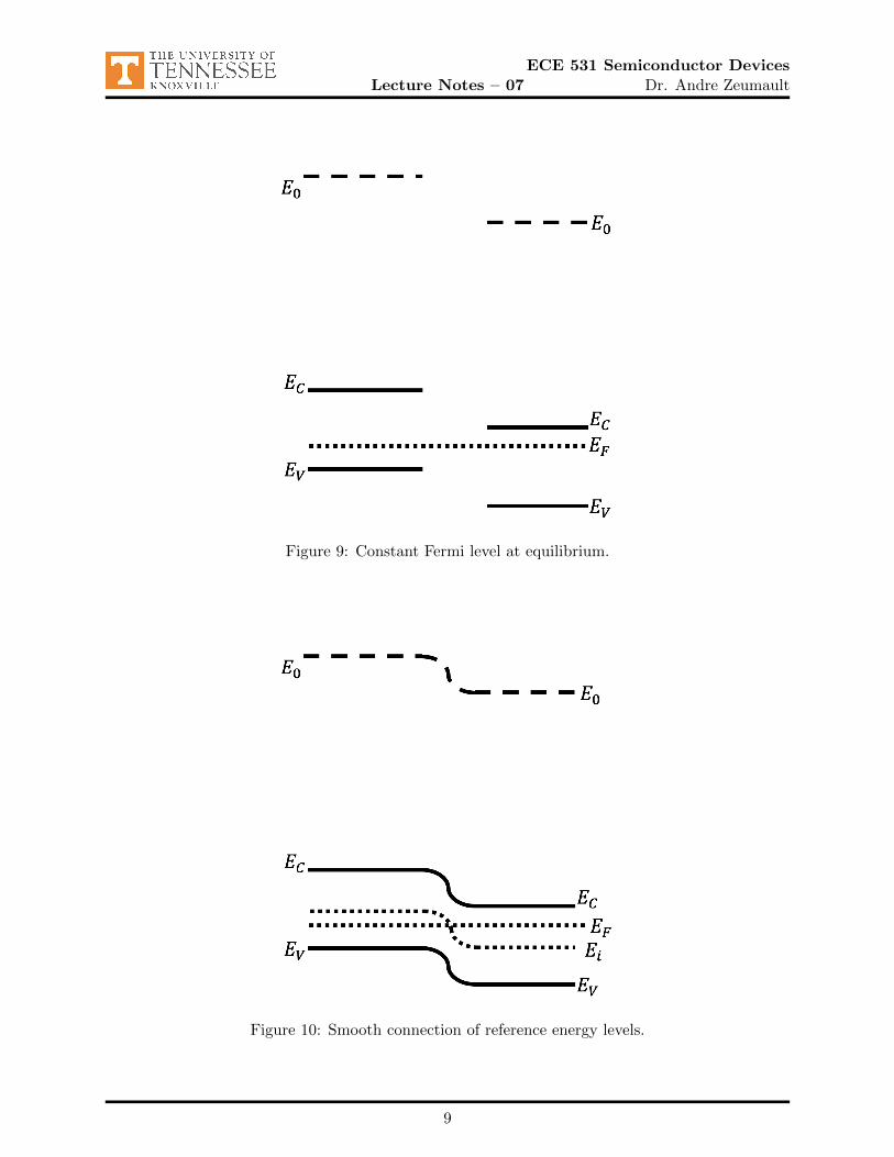
Figure 12: Illustration of the depletion approximation made in a pn-junction
The built-in potential increases logarithmically with dopant concentration
In the above calculation n0(xn) represents the electron concentration on the n-side and n0(−xp)represents the electron concentration on the p-side. Within the Boltzmann approximation, and inthe absence of dopant compensation, these are given by:
n0(xn) ≈ N+D
n0(−xp) ≈n2iN−A
3.5 Depletion Approximation
The depletion approximation assumes that there are no mobile charge carriers in the spacecharge region and that the net charge density outside of the SCR is zero. The region outside of theSCR is referred to as the quasi-netural region. This assumption leads to an analytic closed-formsolution to Poisson’s equation that is portable to device analysis.
The depletion approximation ignores mobile charges in the SCR.
We can visualize the depletion approximation in Figure 12.
4 Quantitative Electrostatics
4.1 Device Geometry and Definitions
The quantitative analysis is based on the following assumptions of device geometry, shown inFigure 13.
• We define as positive, the current I flowing iton the p side and out of the n side.
• The applied voltage VA is the voltage dropped across the p-n junction.
• The contacts are assumed to be Ohmic (linear I-V relationship) and have no resistance unlessexplicitly assumed.
11

Lecture Notes – 07ECE 531 Semiconductor Devices
Dr. Andre Zeumault
Figure 13: Geometry of diode, assumed in subsequent analysis.
• The metallurgical junction, xj is taken to be located at x = 0.
4.2 Equilibrium (VA = 0)
Under equilibrium conditions, the applied voltage, VA is equal to zero. In such a case, we areinterested in mathematical relationships between the charge density, electric field and potential.
At equilibrium, VA = 0
The charge density, within the depletion approximation is given as follows:
ρ(x) =
−eN−
A −xp < x < 0eN+
D 0 < x < xn0 elsewhere
Poisson’s equation, is then given by:
dE
dx=
− eN−
Aεs
−xp < x < 0eN+
Dεs
0 < x < xn0 elsewhere
The solution to this equation is found by integration, and noting that the electric field mustvanish far away from the junction.
E =
− eN−
Aεs
(x+ xp) −xp < x < 0eN+
Dεs
(x− xn) 0 < x < xn0 elsewhere
From electricity and magnetism, we know that the displacement field must be continuous across aninterface, except in the case where an infinite sheet of charge is present. Equating the expressions
12

Lecture Notes – 07ECE 531 Semiconductor Devices
Dr. Andre Zeumault
for the electric field at either side of the metallurgical junction yields the following:
εsE (0−) = εsE (0+)
−eN−
A
εsxp = −
eN+D
εsxn
N−A xp = N+
Dxn
This is just a rehashing of Gauss’ law. By Gauss’ law, the electric field has to vanish far awayfrom the junction, since the net charge within the SCR is zero. To an observer located very faraway from the junction, the SCR looks neutral, much like an electron and a hole would look froman infinite distance, and would therefore not exert an electric field. The electric field is thereforeconfined to the SCR.
Now that we have the electric field, we can integrate it to find the potential.
−dφdx
=
− eN−
Aεs
(x+ xp) −xp < x < 0eN+
Dεs
(x− xn) 0 < x < xn0 elsewhere
φ =
0 x ≤ −xpeN−
A2εs
(x+ xp)2 −xp < x < 0
φbi −eN+
D2εs
(x− xn)2 0 < x < xnφbi x ≥ xn
The depletion width is a useful parameter that defines the total spatial extent of the spacecharge region (SCR). One can show that the widths are specified as follows:
xn =
√√√√2εse
φbi
N+D
(1 +
N+D
N−A
) ∝√φbixp =
√√√√2εse
φbi
N−A
(1 +
N−A
N+D
) ∝√φbiW = xn + xp =
√√√√2εse
φbiN−
AN+D
N−A+N+
D
∝√φbi
The term in the denominator of the expression for the depletion width, W , is essentially equivalentto a parallel combination of resistors. In such cases, this corresponds to an inverse sum and thesmaller of the two parameters will dominate. Therefore, we have, under the following circumstances.
W ≈√
2εse
φbi
N−A
N−A << N+
D
W ≈√
2εse
φbi
N+D
N+D << N−
A
13

Lecture Notes – 07ECE 531 Semiconductor Devices
Dr. Andre Zeumault
Figure 14: Diode under zero bias conditions (equilibrium) VA = 0.
The depletion width is dominated by the lighter doped side of the junction.
4.3 Non-Equilibrium, VA 6= 0
When a voltage is applied, VA 6= 0, and the semiconductor is no longer in equilibrium. To accountfor its effects, the built in potential is replaced with the following:
φbi =⇒ φbi − VA
Simply speaking, the use of a positive applied potential VA > 0 lowers the built-in potential. Whenthe polarity of the applied potential is reversed VA < 0 (or equivalently VR = −VA > 0), the appliedpotential increases the built-in potential.
xn =
√√√√2εse
φbi − VAN+D
(1 +
N+D
N−A
) ∝√φbi − VAxp =
√√√√2εse
φbi − VAN−A
(1 +
N−A
N+D
) ∝√φbi − VAW = xn + xp =
√√√√2εse
φbi − VAN−
AN+D
N−A+N+
D
∝√φbi − VA
VA = −VR
4.3.1 Zero Bias Conditions (VA = 0)
The band diagram under zero-bias is shown in Figure 14. We have discussed this at length in detailand will therefore move on to what happens under non-equilibrium conditions.
14

Lecture Notes – 07ECE 531 Semiconductor Devices
Dr. Andre Zeumault
Figure 15: Diode under forward bias conditions (non-equilibrium) VA > 0. The height of thepotential energy barrier is reduced due to the applied voltage.
4.3.2 Forward Bias Conditions (VA > 0)
The band diagram under zero-bias is shown in Figure 15. Under forward bias conditions, theapplied voltage subtracts from built-in potential, and therefore lowers the energy barrier preventingelectron/hole diffusion across the junction.
The energy barrier preventing electron diffusion from the n to the p side is:EC(xn)− EC(−xp)
This results in a diffusion current that dominates the total diode current flowing underforward biasing conditions. In the next lecture, we will quantify the magnitude of this currentcomponent. It is sufficient to say from the band diagram that the height of this energy barrier,determined from the difference in conduction band levels across the junction, is what primarilydetermines whether or not current flows.
4.3.3 Reverse Bias Conditions (VA < 0)
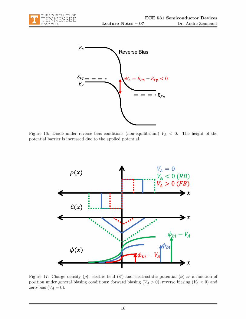
The band diagram under zero-bias is shown in Figure 16. Under reverse bias conditions, the appliedvoltage adds to the built-in potential, and therefore increases the energy barrier preventing elec-tron/hole diffusion across the junction. This results in a substantial suppression of the total diodecurrent. Eventually, the height of this barrier no longer has an incremental effect on suppressingthe current. This occurs when the barrier is much larger than the average thermal energy of chargecarriers.
Current flow under reverse bias is approximately constant!
A summary of the electrostatics under non-equilibrium is shown in Figure 17.
4.3.4 Breakdown
Semiconductors are sensitive, they cannot sustain arbitrarily large electric fields, although it wouldbe nice if they could! In a diode, we designate as breakdown, the voltage (or field) at which thereis a large spike in current under reverse biasing conditions. (Figure 18)
15
Lecture Notes – 07ECE 531 Semiconductor Devices
Dr. Andre Zeumault
Figure 16: Diode under reverse bias conditions (non-equilibrium) VA < 0. The height of thepotential barrier is increased due to the applied potential.
Figure 17: Charge density (ρ), electric field (E ) and electrostatic potential (φ) as a function ofposition under general biasing conditions: forward biasing (VA > 0), reverse biasing (VA < 0) andzero-bias (VA = 0).
16

Lecture Notes – 07ECE 531 Semiconductor Devices
Dr. Andre Zeumault
Figure 18: An illustration of the breakdown process due to quantum mechanical tunneling, and thecorresponding IV relationship. (Hu 1st edition)
Figure 19: An example application of a 3.7 V Zener diode in an electrical circuit. (Hu 1st edition).
Why does breakdown occur? By inspection of Figure 16, it is clear that the effective bandgapenergy narrows near the metallurgical junction, increasingly so as the magnitude of the reverse biasis increased. This narrowing places an extremely large number of electrons (5× 1022 cm−3 to beexact) in very close vicinity to ≈ Nc empty states in the conduction band on the n side. As a result,a process known as band-to-band tunneling occurs between electrons in the valence band on thep side and empty states in the conduction band on the n side. Tunneling is a quantum mechanicaleffect whereby energy is transferred through a barrier to which there is no simple classical analogousdescription. The tunneling process depends on the height and width of the energy barrier involved– the smaller the barrier width/height the larger the tunneling probability.
It turns out that there is some practical utility to breakdown. When certain manufacturersare able to very precisely define a materials breakdown voltage, we create what are known asZener diodes. A Zener diode is just a reverse biased diode that is placed across a sensitive circuitcomponent (Figure 19). Since the current spikes at breakdown, there is very little additional voltagedrop beyond the breakdown voltage (VBR), and the voltage is effectively pinned at VBR.
17