Embed Size (px)
Citation preview

Outline – Sequential Circuitsq• Introduction• Flip-Flops
– RS– JKJK – D
• Latches / BuffersCounters• Counters
• Shift Registers• Other Useful Devices
– 555 Timer– 7-Segment Display
• Finite State MachinesFinite State Machines– Examples
Chapter 7b ME 534 2
Introduction• Logic circuits are classified into two
t icategories:– Combinational logic circuitsg
• Outputs solely depend on the inputs• Combination of basic logic gatesg g
– Sequential logic circuits• Outputs depend not only on the inputs but also theOutputs depend not only on the inputs but also the
history of outputs and/or inputs.• Possess memory characteristicsPossess memory characteristics• Flip-flops (logic gates with feedback connections)
are the basic building blocks
Chapter 7b ME 534 3
g
Flip-Flopsp p• Flip-flops are “memory” elements storing one-bit of
information. • Flip-flops play key role in
– Storing information– Counting– Data sequencing– TimingTiming
• Can be wired from basic logic gates (like NAND).– Available in IC form.
• They are categorized into four groups:– Reset-Set Flip-Flop (RS F/F)
Jam Kill Flip Flop (JK F/F)– Jam-Kill Flip-Flop (JK F/F)– Data Flip-Flop (D F/F)– Toggle Flip-Flop (T F/F)
Chapter 7b ME 534 4
RS Flip-Flopp p
Prohibited
No change!No change!
• User can set or reset (clear) the output Q at will.– Asynchronous device
• Circuit holds the one bit of data indefinitely when both inputs are high.
Chapter 7b ME 534 5
p g

Clocked RS Flip-Flopp p
13 S R Q
1 1 - -
1 0 1 0
Mode
ProhibitedQ
Set
CLK
1
1
2
1 0 1 0
0 1 0 1
0 0 No change!
Reset
Hold
1
1
12
4 No change!Disabled 0
• Clock coordinates the actions of independent units in a complex logic circuit.
• Clocked RS F/F operates in a synchronous fashion.– Inputs are in effect when the clock signal goes high.
Chapter 7b ME 534 6
JK Flip-Flopp p• JK F/F is considered as
universal flip-flop. – J (jam) sets the output state, Q
K (kill) i t t it– K (kill) input resets it.
• Device updates its states at the instant when the clockthe instant when the clock signal goes from either – Low to high logic state g g
(positive edge triggered) OR– High to low logic state
(negative edge triggered)
Pulse generator emits a pulse at thetransition points of the clock signal allowing inputs take effect for a short (negative edge triggered).allowing inputs take effect for a shortduration of time.
Chapter 7b ME 534 7
Pulse Generators of JK F/FPositive-Edge Trigger: Negative-Edge Trigger:
YA
Inverter withdelay
CLKY
AInverter with
delayCLK CLK
B B
td l
t
t
delay
tdelay
tt t
t
Chapter 7b ME 534 8
Operating Modes of JK F/Fp gPositive-Edge Triggered: Negative-Edge Triggered:
J K Q
1 1 Q Q
Mode
ToggleQCLK
1 0 1 0
0 1 0 1
0 0
Set
Reset
Hold No change!
No change!
No change!Hold 0 **No change!Hold 1 **
Hold **
Chapter 7b ME 534 9
gHold

JK F/F with Clear & Preset
I 4 6 (d bl F/F i hi ) PR d CLR i dIn 7476 (double F/Fs in chip), PR and CLR inputs are to set and reset the output states of the device in an asynchronous fashion.
Chapter 7b ME 534 10
D Flip-Flopp pLevel Triggered:
Edge Triggered:
Chapter 7b ME 534 11
D F/F with Clear & Preset
D QMode QCLKPR CLR
ProhibitedN h !No change!
I 4 4 (d bl F/F i hi ) PR d CLR i dIn 7474 (double F/Fs in chip), PR and CLR inputs are to set and reset the output states of the device in an asynchronous fashion.
Chapter 7b ME 534 12
Latch• Latch is a collection of level-
iti D fli flsensitive D flip-flops.– Captures n-bit data. – Stores data which is to be later
used by slower devices.
D0
D
Q0
Q
7475
D1
D2
D3
Q0
Q1
Q1
E0-1
E2-3
Chapter 7b ME 534 13
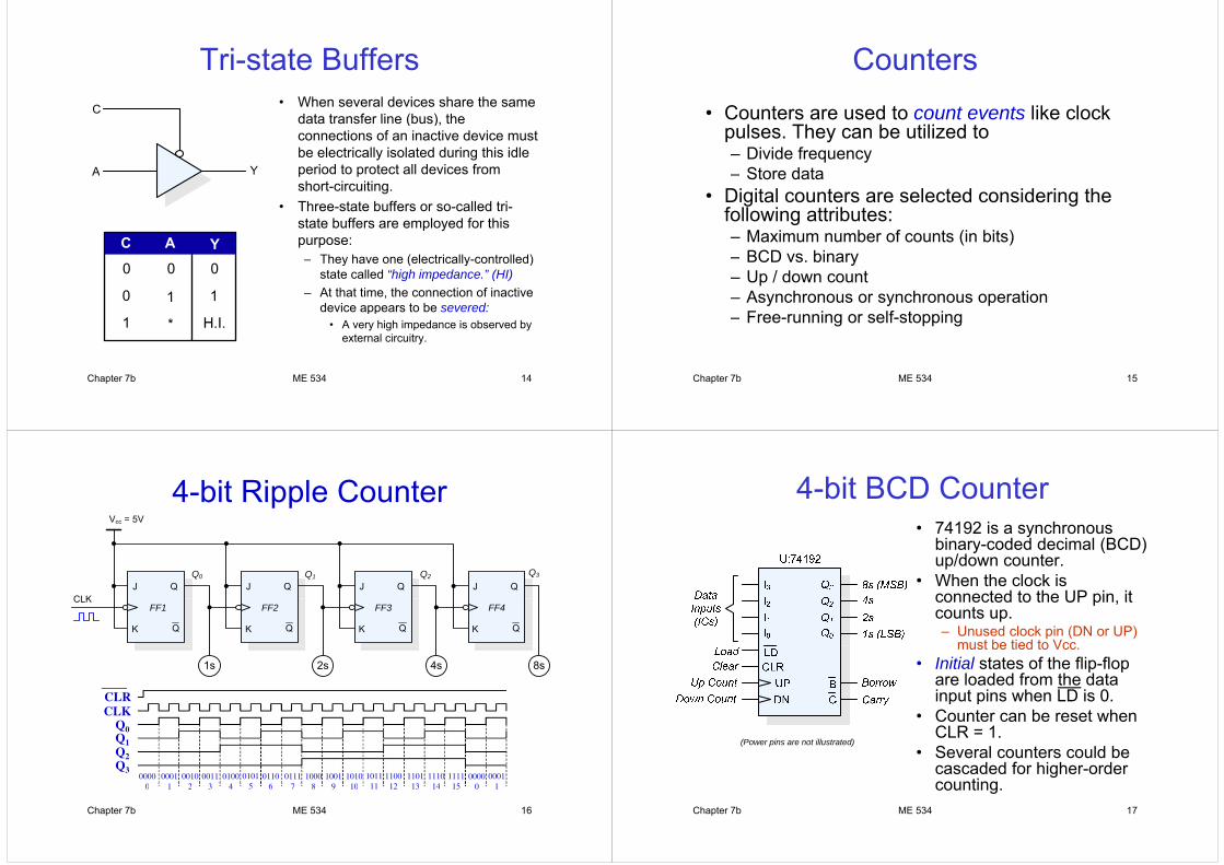
Tri-state BuffersC • When several devices share the same
data transfer line (bus) the
Y
data transfer line (bus), the connections of an inactive device must be electrically isolated during this idle
i d t t t ll d i fA Y period to protect all devices from short-circuiting.
• Three-state buffers or so-called tri-state buffers are employed for this purpose:– They have one (electrically-controlled)They have one (electrically controlled)
state called “high impedance.” (HI)– At that time, the connection of inactive
device appears to be severed:device appears to be severed:• A very high impedance is observed by
external circuitry.
Chapter 7b ME 534 14
Counters• Counters are used to count events like clockCounters are used to count events like clock
pulses. They can be utilized to– Divide frequency– Store data
• Digital counters are selected considering the following attributes:following attributes:– Maximum number of counts (in bits)– BCD vs. binaryBCD vs. binary– Up / down count– Asynchronous or synchronous operation– Free-running or self-stopping
Chapter 7b ME 534 15
4-bit Ripple CounterppVcc = 5V
J Q J QCLK
QJ J QQ3Q2Q1Q0
K Q K Q
CLK
QK K Q
FF1 FF2 FF3 FF4
CLR
8s4s2s1s
Q0Q1
CLKCLR
Q1Q2Q3
00000
00011
00102
00113
01004
01015
01106
01117
10008
10019
101010
101111
110012
110113
111014
111115
00000
00011
Chapter 7b ME 534 16
0 1 2 3 4 5 6 7 8 9 10 11 12 13 14 15 0 1
4-bit BCD Counter• 74192 is a synchronous
binary-coded decimal (BCD) y ( )up/down counter.
• When the clock is connected to the UP pin itconnected to the UP pin, it counts up.– Unused clock pin (DN or UP)
must be tied to Vccmust be tied to Vcc.• Initial states of the flip-flop
are loaded from the data input pins when LD is 0input pins when LD is 0.
• Counter can be reset when CLR = 1.
(Power pins are not illustrated)• Several counters could be
cascaded for higher-order counting
(Power pins are not illustrated)
Chapter 7b ME 534 17
counting.

Two Decimal-Digit Countingg g
V = 5V V
QI
U1:74192
QI
U2:74192
Vcc = 5V Vcc
Q1I1Q2
Q3
I2I3
Q1I1Q2
Q3
I2I3
10s
I0 Q0
LDCLR
I0 Q0
LDCLRCLK CLR
UPDN
BC
CLRUPDN
BC
CLK
Chapter 7b ME 534 18
Resetting CountersgU1:74192 U2:74192
Vcc = 5V Vcc
Q1I1Q2
Q3
I2I3
Q1I1Q2
Q3
I2I3
1s 10s
I0 Q0
LDCLR
I0 Q0
LDCLRCLK
UPDN
BC
UPDN
BC
CLK
External logic elements are employed to reset the counters automatically when a certain count value is reached (say, 60).
Chapter 7b ME 534 19
y ( y, )
Popular ICsp
74279 Q d SR Fli Fl74279: Quad SR Flip-Flop7474: Dual D-type Flip Flop7475 4 bit L t h7475: 4-bit Latch7476: Dual JK-type Flip Flop74125 T i t t B ff74125: Tri-state Buffer74163: 4-bit Binary Counter74192 4 bit BCD C t74192: 4-bit BCD Counter7493: 4-bit Binary Counter
Chapter 7b ME 534 20
Shift Registersg• Shift registers are used for sequencing and
interfacing between serial and parallel communicationinterfacing between serial and parallel communication systems.
• Binary sequence is shifted left or right at each clock• Binary sequence is shifted left or right at each clock pulse.– While shifting, the register must hold the content of the g g
shifted data.
• The registers are classified as– Serial-in serial-out (SISO) shift registers – Parallel-in serial-out (PISO) shift registers
Serial in parallel out (SIPO) shift registers– Serial-in parallel-out (SIPO) shift registers– Parallel-in parallel-out register (or simply “register”)
Chapter 7b ME 534 21

Shift RegistersgSerial in / Serial out:
Parallel in1 0 1 1 0 1 0 0
S i l t
Parallel in / Serial out:
0 0 1 ...1 0 1 1 0 1 0 0Serial out
Serial in / Parallel out: Parallel out1 0 1 1 0 1 0 0
... 0 1 0Serial in
1 0 1 1 0 1 0 0
Chapter 7b ME 534 22
4-bit SISO (Right) Shift Register( g ) g
Chapter 7b ME 534 23
4-bit SISO (Left) Shift Register( ) g
SerialSerial
D Q D Q D Q D QQ3 Q2 Q1 Q0
FF1 FF2 FF3
Serial Input
Serial Output
FF4
Clock
Serial out Serial inQ3 Q2 Q1 QSerial out Serial inQ3 Q2 Q1 Q0
Chapter 7b ME 534 24
Shift Register ICsg
• Some comercially available shift registers areare– 7495: 4-bit shift register
74164 8 bit i l i ll l t– 74164: 8-bit serial in, parallel out– 74165: 8-bit serial/parallel-in serial out– 74195: 4-bit parallel access
Chapter 7b ME 534 25

Timers
R li bl ti i hi h i t h i th• Reliable timing source, which is to synchronize the operation of various units of the circuit, is needed in digital circuitsdigital circuits.
• For simple logic circuits, 555 timer, which has a timing range from μs to minutes, is utilized.range from μs to minutes, is utilized.
• It has two operation modes:– Astable (free running) multivibrator( g)– Mono-stable (one-shot) multivibrator
• The timing parameters of the device is adjusted via two resistances and a capacitor.
Chapter 7b ME 534 26
LM555VCC = +5VVCC
10nFU1: 555
VCC
The parameters of the circuit1
10nF8
72 RA
GND
Trig.
Vcc
Dischg.
pare determined using thefollowing expressions:
10 F
6
54
3
RB
VoutReset +
Out Thres.
Ctrl. CRRt BAH )(695.0 +=
C
10nF+ CRt BL 695.0=
f 44.1CRR
fBA )2(695.0 +
=
Chapter 7b ME 534 27
Schmitt Trigger as Clock Sourcegg• Schmitt trigger
V V
5V
Vout
incorporates a hysteresis loop (relay) and is frequently employed:
Vin Vout
V VVinfrequently employed:
– to filter glitches– to shape up slowly varying
5
VinVout
VT- VT+
to shape up slowly varying signals
• For time-insensitive 3
4
[V
]
applications, an inverting Schmitt trigger (like 7414) could be utilized to 1
2Vol
tage
VT+ (1.7 V)
VT (0.9 V)could be utilized to generate a clock signal.
0
1
T- ( )
Chapter 7b ME 534 28
0 1 2 3 4 5 6 7 8 9 10Time [s]
7414 Schmitt Trigger (Cont’d)gg ( )
R 1 MΩ ; C 1 μF
4
4.5
5
R = 1 MΩ ; C = 1 μF
2 5
3
3.5
e [V
]
1.5
2
2.5
Vol
tage
Vin
Vout
With R and C values, one can
0 0 5 1 1 5 2 2 5 3 3 5 4 4 5 50
0.5
1select the oscillation frequencyof output voltage waveform:
0 0.5 1 1.5 2 2.5 3 3.5 4 4.5 5Time [s]
RCfosc ⋅
=853.01
Chapter 7b ME 534 29

7 Segment Displaysg p yCommon Anode: (LS 5025)
Common Cathode: (LS 5015)
Chapter 7b ME 534 30
Seven-segment Decoderg
• 7447 decoder is frequently7447 decoder is frequently used to drive a 7-segment display.
U:7447
aA0
• Input to the decoder is a 4-bit BCD.
bcd
BCDNumber
A1
A2
A3
• Its outputs are connected to the corresponding pins f ( d ) 7
LTBIRBI
defg
LED Test
Blanking
Ripple Blanking of a (common-anode) 7-segment display.
• Display is active when all(Power pins are not illustrated)
RBI gRipple Blanking
• Display is active when all control inputs are high.
Chapter 7b ME 534 31
Example – 7 Segment Displayp g p ycc cccc cc
0
1
2
3
Chapter 7b ME 534 32
Finite State Machines
• Logic circuits with memory– Outputs = f(inputs, past inputs, past outputs)– Such circuits have finite states:
• State indicates the state of a memory device (F/Fs) in circuit.• State is generally an input or an output to a combinational
logic circuit.
Circuit goes thru a sequence of states in a cycle– Circuit goes thru a sequence of states in a cycle.• Different actions are performed at each state.
– Example: Door combination lockExample: Door combination lock
Chapter 7b ME 534 33

FSM ArchitecturesTwo types of FSM architectures are commonly used:
D1
RegisterMoore FSM:Mealy FSM:
Q11
Q2D2
QDN
Q1D1
QN
Cl k
QN
DN
ClockClock
Chapter 7b ME 534 34
State Transition Diagramsg• State transition diagrams
X * / Y *
X = * X = *
State transition diagrams(STD) are used to visualize/analyze the operation of an FSM
1X = * / Y = *
2operation of an FSM.– Each state (S) is represented
by a circle.
I = * / Y = *X = * / Y = *– Transition from one state to
another is indicated an arrow.• Corresponding inputs (X)
3X = *
4
X = *
p g p ( )necessary to make that transition happen are shown above the arrows. P di l h t t (Y)X = X = • Proceeding a slash, output (Y) at the present state is also given.
Chapter 7b ME 534 35
FSM ModelNext
StatesPresentS
These connections are made if applicable.
Q1D1
D2
PS1NS1
Y1
Y2
X1
X2
States States
Q2D2
PS2
NS2
Y2XI
QN
DN
D F/F
PSNNSNYJ
Clock
• D (Data) F/F is associated with each encoded stateD (Data) F/F is associated with each encoded state.• Combinational input logic generates next set of states.• Outputs depend on present states of machine.
– If necessary inputs are taken into consideration
Chapter 7b ME 534 36
– If necessary, inputs are taken into consideration.
Design Procedureg• Begin with circuit function specifications
V b l d i ti f th i it’ ti– Verbal description of the circuit’s operation• Draw state transition diagram (STD)• Create state transition table (STT)
f f– Tabular form of state diagram– Very similar to truth table
• Decide on the representation of the states (a.k.a. “state encoding”)encoding”)– Use counters whenever possible
• Simplifies the design– Create encoded STT– Create encoded STT
• Derive Boolean expressions for each state• Draw circuit diagram
F/F for each state– F/F for each state– Design combinatorial logic circuits to implement encoding
Chapter 7b ME 534 37

Example 1*p
• Design a circuit for odd-parity checking:• Design a circuit for odd-parity checking:– Accepts a bit stream as input.
If the number of ones in the stream is odd the output– If the number of ones in the stream is odd, the output becomes high (1).
Chapter 7b ME 534 38[*] CS-150 Class Notes, UC Berkeley.
Solution• Before a new bit arrives, the circuit needs to
remember whether the number of bits in previous “step” is even or odd.
f• A natural choice for the states is– Even (0) and Odd (1)
Chapter 7b ME 534 39
Solution (Cont’d)( )State Transition Table: Boolean Expression:
PSOUTINPSNS
=⊕=S
Chapter 7b ME 534 40
Example 2*p• Design the FSM of a
dinewspaper dispenser.– Each newspaper is, say,
15¢.15¢.– Exact change is required to
get the newspaper:(“ ”) 10 (“ ”)• 5¢ (“Nickel”) + 10¢ (“Dime”)
• 5¢ + 5¢ + 5¢• A deposit of 2×10¢ is also p ¢
accepted but no nickel is returned!
– With correct change, theWith correct change, the lock of the dispenser is to be released.
Chapter 7b ME 534 41[*] CS-150 Class Notes, UC Berkeley.

Solution• Inputs: N (Nickel) and D (Dime)
– Lock mechanism generates RESET.St t 0¢ 5¢ 10¢ d 15¢• States: 0¢, 5¢, 10¢, and 15¢.
• Output: OPENPS D N NS OPENS S
0 010
01
O
0¢5¢
10¢01 10¢
0 010
5¢
10¢01 15¢
0 0 10¢1
-
0
-
15¢
15¢
1 15¢1
Chapter 7b ME 534 42
¢
Solution (Cont’d)( )
• Let us uniquely encode 4 states using two F/Fs:
D NNS
0 0
OPEND1 D0Q1 Q0
PS
0 0
– D1 and D0 are their data inputs (Next states).Q and Q are their
10
01
0
0 0
0 0 0 11 0
10– Q1 and Q0 are their outputs (Present states).
• 0¢ → Q1 = 0; Q0 = 0
0 010
01
00 110
1 01 1
• 5¢ → Q1 = 0; Q0 = 1• 10¢ → Q1 = 1; Q0 = 0• 15¢ → Q1 = 1; Q0 = 1
0 010 0
1 01 0
1 0
1 11 115¢ Q1 1; Q0 1
-- 11 1 1 1
Chapter 7b ME 534 43
Solution (Cont’d)( )Examining STT closely yields Circuit Schematics:
0010
011
'')( NQNQDNQDDNQQD
+++=
++=
01QQOPEN =
Note that a FSMmust be initiallized correctly Hence Setcorrectly. Hence, Setand Reset inputs ofD F/Fs are used toset the initial states ofset the initial states of the circuit.
Chapter 7b ME 534 44
One-hot (State) Encoding( ) g• Thanks to its simplicity, one-hot state encodingThanks to its simplicity, one hot state encoding
are often-time employed in digital circuit design:– One D F/F for each state of the FSMOne D F/F for each state of the FSM– Easy encoding– Simplifies derivation of Boolean expressions– Simplifies derivation of Boolean expressions
• During the operation of the circuit, only one state is active (“hot”) while the remaining ones areis active ( hot ) while the remaining ones are inactive (“cool”).N t ffi i t tili ti f• Not very efficient utilization of resources.
Chapter 7b ME 534 45

Example 2 - Revisitedp• This time, four states will be encoded using four F/Fs:
• 0¢ Q = 0; Q = 0; Q = 0; Q = 1• 0¢ → Q3 = 0; Q2 = 0; Q1 = 0; Q0 = 1• 5¢ → Q3 = 0; Q2 = 0; Q1 = 1; Q0 = 0• 10¢ → Q3 = 0; Q2 = 1; Q1 = 0; Q0 = 0• 15¢ → Q3 = 1; Q2 = 0; Q1 = 0; Q0 = 0
D NNext States
OPEND DQ QPresent States
QQ DD Boolean Terms:D N
0 010
01
OPEN
0
D1 D0Q1 Q0
0 00 000 1
Q2Q3 D2D3
100 11 00 0
000 ''NDQD =
Boolean Terms:
0 010
0
1
0
0 0
01000 001 0
1 00 00 0
1
0 1 0 0
2102
101
)(''
''
QNDQDQDNDQNQDQD
NDQNQD++=
+=
0 01
-
0
-
0
1
1 01 0
1
00
0 00
0 111 0
0 00 00 0
0
0 0 013
3213 )(QOPEN
QNDQDQD=
+++=
Chapter 7b ME 534 46