Embed Size (px)
DESCRIPTION
Outline. Influence of the deposition technique on the properties of CsI photocathodes (PCs) Preliminary results on diamond PCs Concluding remarks. 2. Thermal evaporation (Joule effect) more utilised technique for the CsI - PowerPoint PPT Presentation
Citation preview
55thth International Workshop on RICH, Playa del Carmen, Mexico International Workshop on RICH, Playa del Carmen, Mexico 11stst December, 2004 December, 2004
OutlineOutline
Influence of the deposition deposition techniquetechnique
on the properties of CsICsI photocathodes photocathodes
(PCs)(PCs)
Preliminary results on diamonddiamond PCsPCs
Concluding remarks22
55thth International Workshop on RICH, Playa del Carmen, Mexico International Workshop on RICH, Playa del Carmen, Mexico 11stst December, 2004 December, 2004
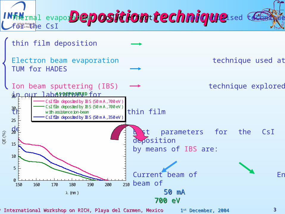
Deposition techniqueDeposition techniqueThermal evaporation (Joule effect) more utilised technique for the CsI thin film deposition
Electron beam evaporation technique used at TUM for HADES
Ion beam sputtering (IBS) technique explored in our laboratory for the first time for the CsI thin film deposition
Best parameters for the CsI film depositionby means of IBS are:
Current beam of Energy beam of 50 mA50 mA 700 eV 700 eV
0
5
10
15
20
25
30
35
150 160 170 180 190 200 210
AS DEPOSITED
CsI film deposited by IBS (50 mA, 700 eV)CsI film deposited by IBS (50 mA, 700 eV) with assistance ion-beamCsI film deposited by IBS (50 mA, 350 eV)
(nm)
33

55thth International Workshop on RICH, Playa del Carmen, Mexico International Workshop on RICH, Playa del Carmen, Mexico 11stst December, 2004 December, 2004
Sample stability against Sample stability against aging aging
due to humid air exposuredue to humid air exposure
CsI photocathodes deposited by IBS seem to be more stablestable after 24 h air exposure than the evaporated ones.
QE (%) IBS < QE (%) thermal evaporation
Comparison between the QE (%) of CsI photocathodes grown with two different techniques: thermal evaporation and IBS in our laboratories, without post-depositionthermal annealing
0
5
10
15
20
25
30
35
150 160 170 180 190 200 210
AS DEPOSITED
CsI film deposited by THERMAL EVAPORATION
CsI film deposited by IBS (50 mA, 700 eV)
(nm)
0
0.05
0.1
0.15
0.2
0.25
0.3
0.35
0.4
CsI film deposited by IBS (50 mA, 700 eV)
CsI film deposited by THERMAL EVAPORATION
150 155 160 165 170 175 180 185 190
(nm)
depositedas
airhumidinhafter
QE
QERQE 24
44

55thth International Workshop on RICH, Playa del Carmen, Mexico International Workshop on RICH, Playa del Carmen, Mexico 11stst December, 2004 December, 2004
Crystalline structure Crystalline structure (XRD)(XRD)
20 25 30 35 40 45 50 55 60 65 70
(200)
Ti/Au substrate
Evaporated CsI film
Co
un
ts (
a.u
.)
2(°)
20 25 30 35 40 45 50 55 60 65 700
250500750
100012501500175020002250250027503000
(220)
Ti/Au
(50 mA, 350 eV) Sputtered
Co
un
ts (
a.u
.)
2(°)
(110)
20 25 30 35 40 45 50 55 60 65 700
1000
2000
3000
4000
5000
6000
7000
8000
9000
10000(50 mA, 700 eV) Sputtered
(220)
Ti/Au
Co
un
ts (
a.u
.)
2(°)
(110)
20 25 30 35 40 45 50 55 60 65 700
500
1000
1500
2000
2500
3000
3500
(50 mA, 700 eV) Sputtered with assistance ion-beam
(200)
Cou
nts
(a.u
.)
2 (°)
(310)(110)
Ti/Au
55
55thth International Workshop on RICH, Playa del Carmen, Mexico International Workshop on RICH, Playa del Carmen, Mexico 11stst December, 2004 December, 2004
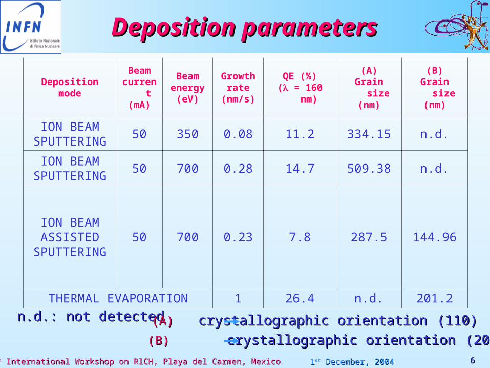
Deposition parametersDeposition parameters
Depositionmode
Beamcurren
t(mA)
Beamenergy
(eV)
Growthrate
(nm/s)
QE (%)( = 160
nm)
(A)Grain size
(nm)
(B)Grain size
(nm)
ION BEAMSPUTTERING
50 350 0.08 11.2 334.15 n.d.
ION BEAMSPUTTERING
50 700 0.28 14.7 509.38 n.d.
ION BEAMASSISTED
SPUTTERING50 700 0.23 7.8 287.5 144.96
THERMAL EVAPORATION 1 26.4 n.d. 201.2
n.d.: not detectedn.d.: not detected (A)(A) crystallographic orientationcrystallographic orientation (110)(110)
(B)(B) crystallographic orientationcrystallographic orientation (200)(200)66
55thth International Workshop on RICH, Playa del Carmen, Mexico International Workshop on RICH, Playa del Carmen, Mexico 11stst December, 2004 December, 2004
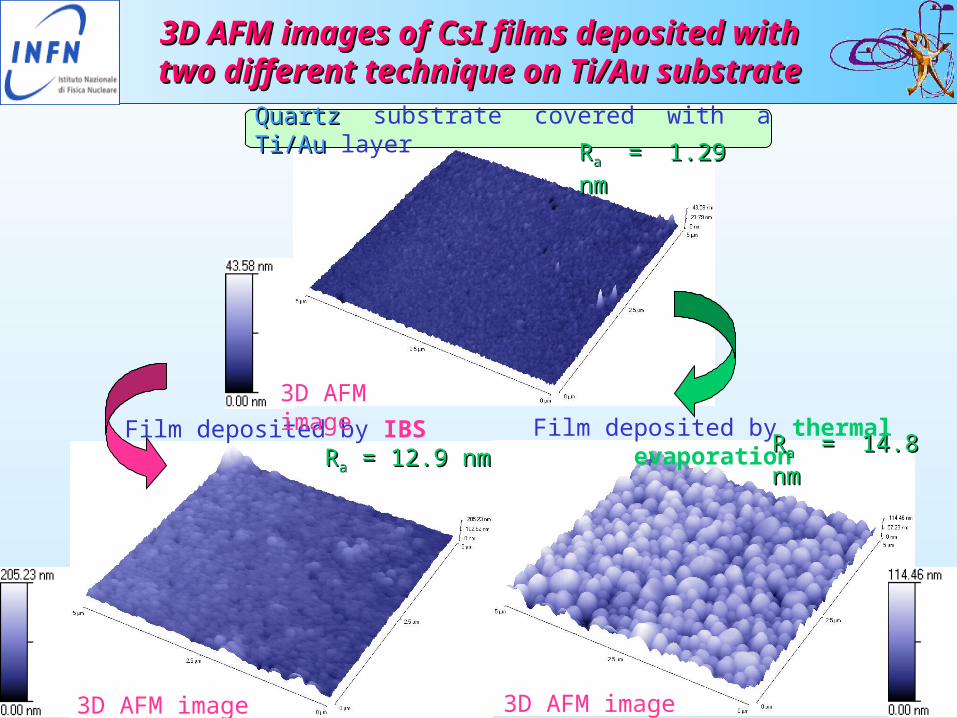
3D AFM images of CsI films deposited 3D AFM images of CsI films deposited with two different technique on Ti/Au with two different technique on Ti/Au
substratesubstrate
3D AFM image
Film deposited by thermal evaporation
3D AFM image
RRaa = 1.29 nm = 1.29 nm
RRaa = 12.9 nm = 12.9 nmFilm deposited by IBS
RRaa = 14.8 = 14.8 nmnm
QuartzQuartz substrate covered with a Ti/Au Ti/Au layer RRaa = 1.29 = 1.29
nmnm
3D AFM image

55thth International Workshop on RICH, Playa del Carmen, Mexico International Workshop on RICH, Playa del Carmen, Mexico 11stst December, 2004 December, 2004
3D AFM images of 3D AFM images of substrates substrates with different roughness Rwith different roughness Raa
RRaa = 12.48 nm = 12.48 nm
RRaa = 350 nm = 350 nm
RRaa = 4.55 = 4.55 nmnm
Quartz Quartz substrate covered withsubstrate covered with an an Al Al layerlayer PCBPCB substrate
PeenedPeened quartz quartz substrate covered withsubstrate covered with an an Au Au layerlayer
88
3D AFM image
3D AFM image
3D AFM image

55thth International Workshop on RICH, Playa del Carmen, Mexico International Workshop on RICH, Playa del Carmen, Mexico 11stst December, 2004 December, 2004
0
5
10
15
20
25
150 160 170 180 190 200 210
CsI films deposited by thermal evaporation
Qz + Al (Ra = 4.55 nm)
Qz + Ti/Au (Ra = 1.29 nm)
Peened Qz + Au ((Ra = 350 nm)
Cern PCB (Ra = 12.48 nm)
(nm)
QE (a.u.) vs. the QE (a.u.) vs. the substrate roughnesssubstrate roughness
The QE (a.u.) of CsI PCs deposited by IBS follows the surface average roughness Ra
of substrates
The QE (a.u.) of CsI PCs deposited by thermal evaporation seems to be independent from the surface average roughness Ra of
substrates,but………………………
0
1
2
3
4
5
6
7
8
150 160 170 180 190 200 210
CsI film deposited by IBS
Qz + Ti/Au (Ra = 1.29 nm)
Qz + Al (Ra = 4.55 nm)
Peened Qz + Au (Ra= 350 nm)
Cern PCB (Ra = 12.48 nm)
(nm)
99
55thth International Workshop on RICH, Playa del Carmen, Mexico International Workshop on RICH, Playa del Carmen, Mexico 11stst December, 2004 December, 2004
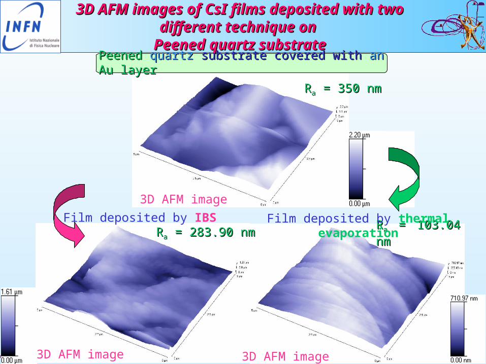
RRaa = 283.90 nm = 283.90 nmFilm deposited by IBS
RRaa = 103.04 = 103.04 nmnm
3D AFM image
3D AFM images of CsI films deposited 3D AFM images of CsI films deposited with two different technique on with two different technique on
Peened quartz substratePeened quartz substratePeenedPeened quartz quartz substrate covered withsubstrate covered with an an Au Au layerlayer
RRaa = 350 nm = 350 nm
3D AFM image 3D AFM image
Film deposited by thermal evaporation

55thth International Workshop on RICH, Playa del Carmen, Mexico International Workshop on RICH, Playa del Carmen, Mexico 11stst December, 2004 December, 2004
3D AFM images of CsI films deposited 3D AFM images of CsI films deposited with two different technique on Al with two different technique on Al
substratesubstrate
RRaa = 4.55 = 4.55 nmnm
Quartz Quartz substrate covered withsubstrate covered with an an Al Al layerlayer
RRaa = 39.82 nm = 39.82 nmFilm deposited by IBS RRaa = 67.49 = 67.49
nmnm
3D AFM image
3D AFM image 3D AFM image
Film deposited by thermal evaporation

55thth International Workshop on RICH, Playa del Carmen, Mexico International Workshop on RICH, Playa del Carmen, Mexico 11stst December, 2004 December, 2004
3D AFM images of CsI films deposited 3D AFM images of CsI films deposited by two different technique on PCB by two different technique on PCB
substratesubstrate
RRaa = 24.09 nm = 24.09 nmFilm deposited by IBS
RRaa = 13.54 = 13.54 nmnm
QuartzQuartz substrate covered with a PCBPCB layer
3D AFM imageFilm deposited by thermal evaporation
RRaa = 12.48 nm = 12.48 nm
3D AFM image 3D AFM image

55thth International Workshop on RICH, Playa del Carmen, Mexico International Workshop on RICH, Playa del Carmen, Mexico 11stst December, 2004 December, 2004
Model of a CsI film morphology deposited on the Model of a CsI film morphology deposited on the same substrate by the two different techniquessame substrate by the two different techniques
(a)(a)Film deposited by
thermal evaporationthermal evaporation
(b)(b)Film deposited by
IBSIBS
Electron photoexcitement
regions
FILM
SUBSTRATO
hv hv
FILM
hvhv UV
Photons
SUBSTRATE SUBSTRATE
hv
2
2cos1
nF
Effective reduction factor of the absorptionabsorption lengthlength:
nn is the refractive index of CsI is the angle between the surface and the direction of the incident radiation
In case (a)(a) there is an enhancement of the maximum efficiency of photoemission for reflectivereflective PCs :
L
LQTQER max FL
LQTQER
max
Q = intrinsic QE T = probability that an electron that reach the surface can escape (T 1)L = escape length = optical absorptionabsorption lengthlength
1010
55thth International Workshop on RICH, Playa del Carmen, Mexico International Workshop on RICH, Playa del Carmen, Mexico 11stst December, 2004 December, 2004
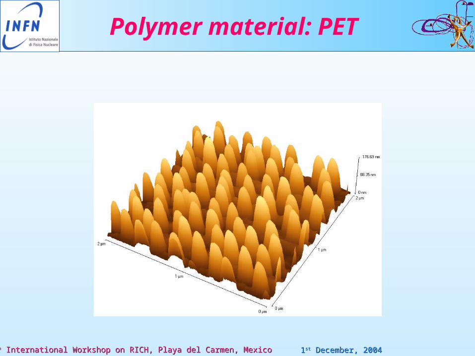
Polymer material: PET

55thth International Workshop on RICH, Playa del Carmen, Mexico International Workshop on RICH, Playa del Carmen, Mexico 11stst December, 2004 December, 2004
Progress in diamond films for the Progress in diamond films for the realization of UV photocathodesrealization of UV photocathodes
PHOTOCATHODEPHOTOCATHODE = key element of many detectiondetection systems
Since many years the scientific research has been devoted to the study of materialsmaterials for the PCPC production, depending on the spectral rangespectral range of detection.
For the UV UV range, PCsPCs manufactured with alternativealternative materials with respect to CsI have to present the following properties:
– quantum efficiency comparablecomparable to that of CsICsI PCsPCs;
exposure to high photon or ion flux– high stability stability for exposure in air
1212
55thth International Workshop on RICH, Playa del Carmen, Mexico International Workshop on RICH, Playa del Carmen, Mexico 11stst December, 2004 December, 2004
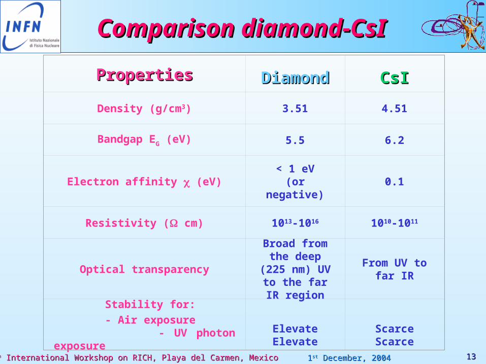
Comparison diamond-CsIComparison diamond-CsI
PropertiesProperties DiamonDiamondd
CsICsI
Density (g/cm3)
3.51 4.51
Bandgap EG (eV)
5.5 6.2
Electron affinity (eV)< 1 eV
(or negative)
0.1
Resistivity ( cm)
1013-1016
1010-1011
Optical transparency
Broad from the deep
(225 nm) UV to the far IR
region
From UV to far IR
Stability for:- Air exposure
- UV photon exposureElevateElevate
ScarceScarce
1313
55thth International Workshop on RICH, Playa del Carmen, Mexico International Workshop on RICH, Playa del Carmen, Mexico 11stst December, 2004 December, 2004
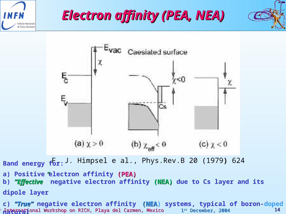
Electron affinity (PEA, NEA)Electron affinity (PEA, NEA)
Band energy for: a) Positive electron affinity (PEA)(PEA) b) “Effective“Effective”” negative electron affinity (NEA) (NEA) due to Cs layer and its dipole
layer c) “True”“True” negative electron affinity (NEA(NEA) systems, typical of boron-doped natural diamond
F. J. Himpsel e al., Phys.Rev.B 20 (1979) 624
1414

55thth International Workshop on RICH, Playa del Carmen, Mexico International Workshop on RICH, Playa del Carmen, Mexico 11stst December, 2004 December, 2004
QE (%) of an amourphous QE (%) of an amourphous diamonddiamond
film deposited by means of IBSfilm deposited by means of IBS
Proceedings SPIE, vol. 4139, San Diego, California (2000)
A.S. Tremsin* and O.H.W. Siegmund0.01
0.1
1
150 160 170 180 190 200 210
Ion Beam Sputtered DLC
QE
(%)
(nm)
Literature (Literature (POLYPOLYCRYSTALLINE CRYSTALLINE film)film)@ = 1500 Å QE (%) = 0.2
%
Our results (Our results (IBSIBS diamonddiamond filmfilm – – Bari Bari --))@ = 150 nm QE (%) = 0.7 %
1919

55thth International Workshop on RICH, Playa del Carmen, Mexico International Workshop on RICH, Playa del Carmen, Mexico 11stst December, 2004 December, 2004
Substrates usedSubstrates used
Silicon (Si) substrates were used for the diamand film deposition because of their cubic crystalline
structure, as that of diamond.
BeforeBefore proceeding to the deposition of diamond film, it is important to treat the surface of Si
substrate with diamond powder diamond powder in ultrasonic bathultrasonic bath..
Si Si not not treated, in fact, presents: low density of nucleation centres (104 cm-2) due to the high surface energy of
diamond, the big mismatch between Si and diamond and the low probability of nucleation precursor sticking.
Si Si traitedtraited with diamond powderdiamond powder presents: high density of nucleation centres (1011 cm-2)
At the LIMHP of Paris, nanocrystalline diamand films with different percentage of graphite were deposited by MPECVD on quartz substrate too.
(a) Si substrate notnot traited (b) Si substrate traited with AlAl22OO3 3 powder
(c) Si substrate traited with SiC SiC powder
(d) Si substrate traited with diamaond diamaond
polwderpolwder
1515

55thth International Workshop on RICH, Playa del Carmen, Mexico International Workshop on RICH, Playa del Carmen, Mexico 11stst December, 2004 December, 2004
Techniques of deposition for Techniques of deposition for diamond filmsdiamond films
PolyPoly and nanonanocrystallinecrystalline diamond films were prepared by MPECVDMPECVD, at the LIMHP (Laboratoire d’Ingénierie des Materiaux et des Hautes Pressions) - CNRS-UPR- Paris.
MPECVDMPECVD:: microwavemicrowave plasma plasma enhancedenhanced chemical vapour depositionchemical vapour deposition
AmorphousAmorphous diamond films were prepared by IBSIBS, at the Thin Film Laboratory of Bari, starting from a carbon target.
CH4/H2 plasma discharge conditions, adopted in experiment of diamond deposition are:1. reactor UHV coupled to a microwave generator (2.45 GHz)2. CH4 highly diluited in H2 (CH4 < 4%)3. high deposition temperature (750-900 °C) 4. high microwave input power (0.45-2.5 kW) 5. high pressure (10-200 mbar)
1616
55thth International Workshop on RICH, Playa del Carmen, Mexico International Workshop on RICH, Playa del Carmen, Mexico 11stst December, 2004 December, 2004
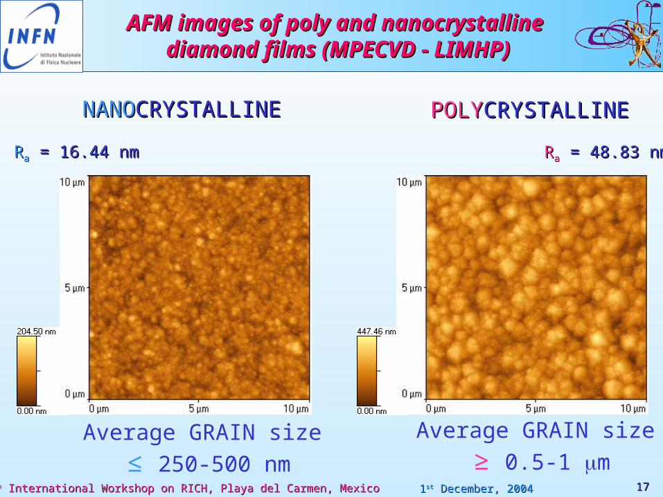
AFM images of poly and nanocrystallineAFM images of poly and nanocrystalline diamond films (MPECVD - LIMHP) diamond films (MPECVD - LIMHP)
NANONANOCRYSTALLINECRYSTALLINE POLYPOLYCRYSTALLINECRYSTALLINE
Average GRAIN size ≤ 250-500 nm
RRaa = 16.44 nm = 16.44 nm RRaa = 48.83 nm = 48.83 nm
Average GRAIN size ≥ 0.5-1 m
1717

55thth International Workshop on RICH, Playa del Carmen, Mexico International Workshop on RICH, Playa del Carmen, Mexico 11stst December, 2004 December, 2004
Comparison with Comparison with literatureliterature
Proceedings SPIE, vol. 4139, San Diego, California (2000)
A.S. Tremsin* and O.H.W. Siegmund
0
5
10
15
20
25
30
150 160 170 180 190 200 210
Diamond films
Ech 4 graphitic NANO (890 ° C)Ech 3 POLY (880 ° C)Ech 2 NANO (815 ° C)Ech 1 NANO (800 ° C)
Wavelength (nm)
Our results (Our results (MPECVDMPECVD diamond diamond film – film – ParisParis--))
LiteratureLiterature
@ = 1500 Å QE (%) = 0.2 %
@ = 150 nm QE (%) = 5 30 %
1818
55thth International Workshop on RICH, Playa del Carmen, Mexico International Workshop on RICH, Playa del Carmen, Mexico 11stst December, 2004 December, 2004
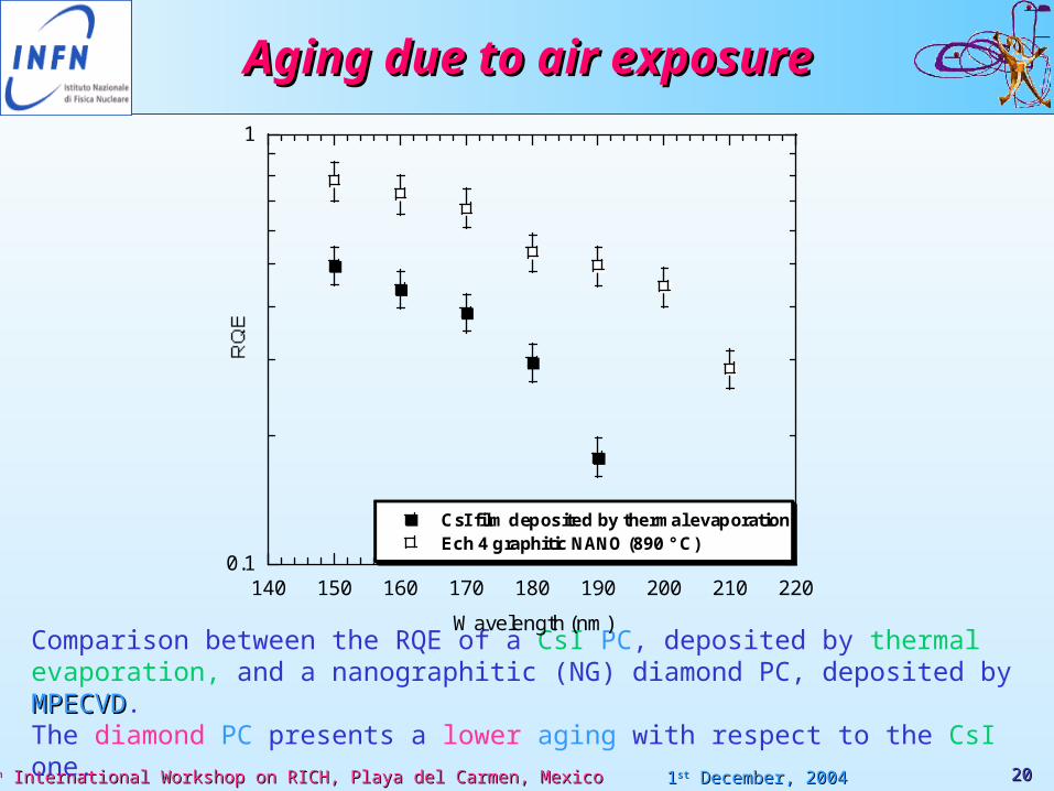
Aging due to air exposureAging due to air exposure
Comparison between the RQE of a CsI PC, deposited by thermal evaporation, and a nanographitic (NG) diamond PC, deposited by MPECVDMPECVD. The diamond PC presents a lower aging with respect to the CsI one.
2020
0.1
1
140 150 160 170 180 190 200 210 220
CsI film deposited by thermal evaporationEch 4 graphitic NANO (890 ° C)
Wavelength (nm)
55thth International Workshop on RICH, Playa del Carmen, Mexico International Workshop on RICH, Playa del Carmen, Mexico 11stst December, 2004 December, 2004
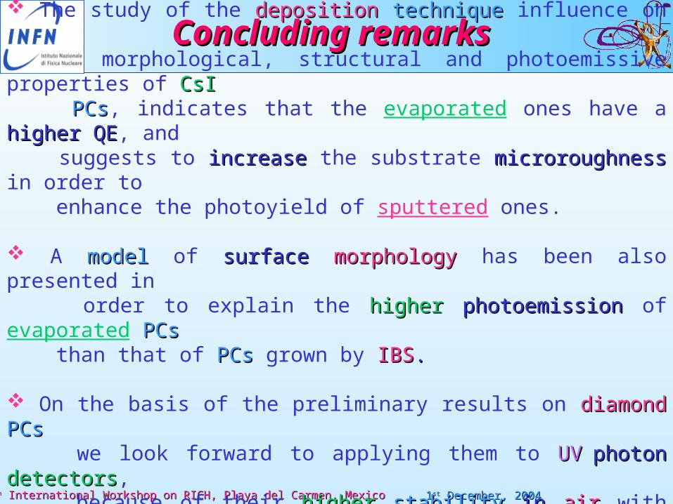
Concluding remarksConcluding remarks The study of the depositiondeposition techniquetechnique influence on morphological, structural and photoemissive properties of CsI CsI PCsPCs, indicates that the evaporated ones have a higher QEhigher QE, and suggests to increaseincrease the substrate microroughnessmicroroughness in order to enhance the photoyield of sputtered ones. A modelmodel of surfacesurface morphology morphology has been also presented in order to explain the higher higher photoemissionphotoemission of evaporated PCs PCs than that of PCsPCs grown by IBSIBS..
On the basis of the preliminary results on diamonddiamond PCsPCs we look forward to applying them to UVUV photonphoton detectorsdetectors, because of their higherhigher stability stability in in airair with respect to that of the detectorsdetectors based on CsI CsI PCsPCs.

55thth International Workshop on RICH, Playa del Carmen, Mexico International Workshop on RICH, Playa del Carmen, Mexico 11stst December, 2004 December, 2004
Thank you
for your attention
and
see YOU at
RICH 2006

55thth International Workshop on RICH, Playa del Carmen, Mexico International Workshop on RICH, Playa del Carmen, Mexico 11stst December, 2004 December, 2004

55thth International Workshop on RICH, Playa del Carmen, Mexico International Workshop on RICH, Playa del Carmen, Mexico 11stst December, 2004 December, 2004

55thth International Workshop on RICH, Playa del Carmen, Mexico International Workshop on RICH, Playa del Carmen, Mexico 11stst December, 2004 December, 2004
Photon-agingPhoton-aging (UV flux : 10 (UV flux : 1077
photons/mmphotons/mm22sec)sec)Before exposure
After exposure
Channeling mechanism
Substrate
PhotoelectronUV
photon
Grains
1
10
100
150 160 170 180 190 200
(nm)
PHOTON AGING UNDER VACUUM
As deposited
Aged after 5 days


![[ Outline ]](https://img.pdfslide.us/doc/110x75/56815a74550346895dc7db61/-outline--56b49f971d862.jpg)