Embed Size (px)
Citation preview

AP7361C Document number: DS37274 Rev. 4 - 2
1 of 22 www.diodes.com
January 2018 © Diodes Incorporated
AP7361C
AD
VA
NC
E IN
FO
RM
AT
IO
N
NE
W P
RO
DU
CT
1A LOW DROPOUT ADJUSTABLE AND FIXED-MODE REGULATOR WITH ENABLE
Description
The AP7361C is a 1A, adjustable and fixed output voltage, ultra-low
dropout linear regulator with enable. The device includes pass
element, error amplifier, band-gap reference, current limit and thermal
shutdown circuitry. The device is turned on when EN pin is set to logic
high level.
The characteristics of the low dropout voltage and low quiescent
current make it suitable for low to medium power applications, for
example, laptop computers, audio and video applications and battery
powered devices. The typical quiescent current is approximately
60µA. Built-in current-limit and thermal-shutdown functions prevent
IC from damage in fault conditions.
The AP7361C is available in U-DFN3030-8 (Type E), SOT89-5,
SOT223, TO252 (DPAK) and SO-8EP packages.
Features
Wide Input Voltage Range: 2.2V to 6.0V
Output Voltage Accuracy: ±1%
Very Low Dropout Voltage (3.3V): 360mV at 1A Typical
Low Quiescent Current (IQ): 60µA Typical
Adjustable Output Voltage Range: 0.8V to 5.0V
Fixed Output Options: 1.0V, 1.2V, 1.5V, 1.8V, 2.5V, 2.8V and
3.3V
High PSRR: 75dB @ 1kHz
Current Limit: 1.5A
Fold-Back Short Circuit Protection: 400mA
Thermal Shutdown Protection
Stable with MLCC, E-Cap, Tan-Cap or Solid Capacitor 2.2µF
Ambient Temperature Range: -40°C to +85°C
Available in “Green” Molding Compound (No Br, Sb)
Totally Lead-Free & Fully RoHS Compliant (Notes 1 & 2)
Halogen and Antimony Free. “Green” Device (Note 3)
Applications
LCD-TV, Monitor
Set-Top-Box
Home Electrical Appliances
Pin Assignments
(Top View) (Top View)
1
2
3
4
8
7
6
5
GND
OUT
NC
ADJ/NC
GND EN
NC
IN
NC
1
2
3 4
5EN
GND
ADJ/NC IN
OUT
GND
U-DFN3030-8 (Type E) SOT89-5
(Top View) (Top View)
1
2
3
IN
GND
OUT
1
2
3
GND
OUT
IN
SOT223 SOT223R
(Top View) (Top View)
IN
NC
NC
NC
EN
OUT
GND
NC
8
7
6
5
1
2
3
4
IN
NC
NC
EN
ADJ/NC
OUT
NC
GND
8
7
6
5
1
2
3
4
SO-8EP SO-8EPR
(Top View) (Top View)
1
2
3
IN
GND
OUT
1
2
3 IN
GND
OUT
TO252 (DPAK) TO252 (DPAK) R
Notes: 1. No purposely added lead. Fully EU Directive 2002/95/EC (RoHS), 2011/65/EU (RoHS 2) & 2015/863/EU (RoHS 3) compliant.
2. See https://www.diodes.com/quality/lead-free/ for more information about Diodes Incorporated’s definitions of Halogen- and Antimony-free, "Green" and
Lead-free.
3. Halogen- and Antimony-free "Green” products are defined as those which contain <900ppm bromine, <900ppm chlorine (<1500ppm total Br + Cl) and
<1000ppm antimony compounds.

AP7361C Document number: DS37274 Rev. 4 - 2
2 of 22 www.diodes.com
January 2018 © Diodes Incorporated
AP7361C
AD
VA
NC
E IN
FO
RM
AT
IO
N
NE
W P
RO
DU
CT
Typical Applications Circuit
COUT
4.7µF
Fixed Version with EN
CIN
4.7µF
IN
GND
EN
OUT
Enable
VIN VOUT
AP7361C
COUT
4.7µF
Fixed Version without EN
CIN
4.7µF
IN
GND
OUT
VIN VOUT
AP7361C
CIN
4.7µF
IN
GND
EN
OUT
EnableADJ
R2
R1 COUT
4.7µF
VIN VOUT
AP7361C
Adjustable Output
Pin Descriptions
Pin Number Pin
Name Function U-DFN3030-8
(Type E) SOT89-5
TO252 (DPAK)
TO252
(DPAK)R SOT223 SOT223R SO-8EP SO-8EPR
8 4 1 3 1 3 8 8 IN The input of the regulator. Bypass to ground through at least 1µF ceramic capacitor.
1 5 3 2 3 2 1 1 OUT
The output of the regulator. Bypass to ground through at least 2.2µF ceramic capacitor. For improved ac load response a larger capacitor is recommended.
4 2 2 1 2 1 4 3 GND Ground
3 3 – – – – – 2 ADJ/NC
Adjustable voltage version only – a resistor divider from this pin to the OUT pin and ground sets the output voltage.
5 1 – – – – 2 5 EN Enable input, active high
2, 6, 7 – – – – – 3, 5, 6, 7 4, 6, 7 NC No connection

AP7361C Document number: DS37274 Rev. 4 - 2
3 of 22 www.diodes.com
January 2018 © Diodes Incorporated
AP7361C
AD
VA
NC
E IN
FO
RM
AT
IO
N
NE
W P
RO
DU
CT
Functional Block Diagram
IN
EN
GND
OUT
Gate
Driver
0.8V
Current Limit
and Thermal
Shutdown
Fixed Version with EN
R
R
IN
GND
OUT
Gate
Driver
0.8V
Current Limit
and Thermal
Shutdown
Fixed Version without EN
R
R
IN
EN
GND
ADJ
OUT
Gate
Driver
0.8V
Current Limit
and Thermal
Shutdown
Adjustable Version

AP7361C Document number: DS37274 Rev. 4 - 2
4 of 22 www.diodes.com
January 2018 © Diodes Incorporated
AP7361C
AD
VA
NC
E IN
FO
RM
AT
IO
N
NE
W P
RO
DU
CT
Absolute Maximum Ratings (@TA = +25°C, unless otherwise specified.) (Note 4)
Symbol Parameter Rating Unit
VIN Input Voltage 6.5 V
– OUT, ADJ, EN Voltage VIN +0.3 V
TJ Operating Junction Temperature Range -40 to +150 °C
TSTG Storage Temperature Range -65 to +150 °C
PD Power Dissipation Internally limited by maximum junction
temperature of +150°C –
PD Power Dissipation
U-DFN3030-8 (Type E) 1700
mW
TO252 (DPAK) 1250
SOT223 1100
SOT89-5 800
SO-8EP 1190
ESD HBM Human Body Model ESD Protection > 2 KV
ESD MM Machine Model ESD Protection (Note 5) > 200 V
Notes: 4. Stresses greater than the 'Absolute Maximum Ratings' specified above may cause permanent damage to the device. These are stress ratings only;
functional operation of the device at these or any other conditions exceeding those indicated in this specification is not implied. Device reliability may be
affected by exposure to absolute maximum rating conditions for extended periods of time.
5. ESD MM rating at 150V for EN pin in SOT89-5 package.
Recommended Operating Conditions (@TA = +25°C, unless otherwise specified.)
Symbol Parameter Min Max Unit
VIN Input Voltage 2.2 6.0 V
VOUT Output Voltage 0.8 5.0 V
IOUT Output Current (Note 6) 0 1.0 A
TA Operating Ambient Temperature -40 +85 C
Note: 6. The device maintains a stable, regulated output voltage without a load current. When the output current is large, attention should be given to the limitation
of the package power dissipation.

AP7361C Document number: DS37274 Rev. 4 - 2
5 of 22 www.diodes.com
January 2018 © Diodes Incorporated
AP7361C
AD
VA
NC
E IN
FO
RM
AT
IO
N
NE
W P
RO
DU
CT
Electrical Characteristics (@TA = +25°C, VIN = VOUT +1V, CIN
= 4.7μF, COUT
= 4.7μF, VEN
= VIN, unless otherwise specified.)
Symbol Parameter Test Conditions Min Typ Max Unit
VREF FB Reference Voltage, ADJ pin IOUT = 10mA, TA = +25°C 0.792 0.8 0.808 V
IADJ ADJ Pin Leakage Current – – 0.1 0.5 µA
IQ Input Quiescent Current Enabled, IOUT = 0A – 60 80 µA
ISHDN Input Shutdown Current VEN = 0V, IOUT = 0A -1 0.05 1 µA
VOUT Output Voltage Accuracy
IOUT = 100mA,
TA = +25°C
1.0V≤VOUT<1.5V VOUT(s)-
0.015 VOUT(s)
VOUT(s)+
0.015 V
1.5 V≤VOUT≤3.3V VOUT(s)*
0.99 VOUT(s)
VOUT(s)*
1.01
OUTIN
OUT
VΔV
ΔV
Line Regulation
VIN = VOUT +1V to 5.5V,
IOUT = 100mA
TA = +25°C – 0.01 0.1 %/V
-40°C ≤TA ≤ +85°C – – 0.2
VOUT / VOUT Load Regulation IOUT from 1.0mA to 1A 1.2V<VOUT≤ 3.3V -1.0 – 1.0 %
1.0V≤ VOUT ≤1.2V -1.5 – 1.5 %
VDROPOUT Dropout Voltage (Note 7)
IOUT = 300mA
1.0V≤VOUT<1.1V – 710 750
mV
1.1V≤VOUT<1.2V – 600 640
1.2V≤VOUT<1.3V – 500 540
1.3V≤VOUT<1.4V – 400 440
1.4V≤VOUT<1.5V – 300 340
1.5V≤VOUT<2.6V – 200 250
2.6V≤VOUT≤3.3V – 90 140
IOUT = 1A
1.0V≤VOUT<1.1V – 840 –
1.1V≤VOUT<1.2V – 780 –
1.2V≤VOUT<1.3V – 710 –
1.3V≤VOUT<1.4V – 660 –
1.4V≤VOUT<1.5V – 610 –
1.5V≤VOUT<2.0V – 570 –
2.0V≤VOUT<2.6V – 440 –
2.6V≤VOUT≤3.3V – 340 –
VIL EN Input Logic Low Voltage – 0 – 0.3 V
VIH EN Input Logic High Voltage – 1.0 – VIN V
RENPD EN Pull-Down Resistor – – 3.0 – MΩ
IEN EN Input Leakage Current VIN = 5.5V, VEN = 0V -0.1 – 0.1 µA
RPD Output Discharge Resistor VOL=1V – 100 – Ω
IOUT Maximum Output Current VIN = VOUT +1V 1.0 – – A
ILIMIT Current Limit VIN = VOUT +1V(VIN MINI=2.2V) 1.1 1.5 – A
ISHORT Short-Circuit Current VIN = VOUT +1V, Output Voltage < 15% VOUT – 400 – mA
PSRR Power Supply Rejection Ratio
(Note 8)
f = 1kHz, IOUT = 100mA – 75 – dB
f = 10kHz, IOUT = 100mA – 55 –
tST Start-Up Time VOUT = 3V, COUT = 2.2µF, RL = 30Ω – 150 – µs
OUTA
OUT
VΔT
ΔV
Output Voltage Temperature Coefficient
IOUT = 100mA, -40°C ≤ TA ≤ +85°C – ±100 – ppm/°C
TSHDN Thermal Shutdown Threshold – – 150 – °C
THYS Thermal Shutdown Hysteresis – – 20 – °C
Notes: 7. Dropout voltage is the voltage difference between the input and the output at which the output voltage drops 2% below its nominal value. This parameter
only applies to output voltages above 1.2V since minimum VIN = 2.2V. 8. For VIN 2.5V and VIN = VOUT +1V. For VIN < 2.5V, the PSRR performance may be reduced.

AP7361C Document number: DS37274 Rev. 4 - 2
6 of 22 www.diodes.com
January 2018 © Diodes Incorporated
AP7361C
AD
VA
NC
E IN
FO
RM
AT
IO
N
NE
W P
RO
DU
CT
Electrical Characteristics (@TA = +25°C, VIN = VOUT +1V, CIN
= 4.7μF, COUT
= 4.7μF, VEN
= VIN, unless otherwise specified.) (Cont.)
Symbol Parameter Test Conditions Min Typ Max Unit
θJA Thermal Resistance Junction-to-Ambient
U-DFN3030-8 (Type E ) (Note 9) – 70 –
°C/W
TO252 (DPAK) (Note 9) – 95 –
SOT223 (Note 9) – 110 –
SOT89-5 (Note 9) – 150 –
SO-8EP (Note 9) – 100 – Note: 9. Test condition: U-DFN3030-8 (Type E), SO-8EP devices are mounted on 2"x2", FR-4 substrate PCB, with minimum recommended pad on top layer and
thermal vias to bottom layer ground plane. TO252(DPAK) devices are mounted on 2"x2" FR-4 substrate PC board, 2oz copper, with minimum recommended pad layout. For SOT223, the device is mounted on FR-4 substrate PC board, with minimum recommended pad layout. SOT89-5 devices are mounted on 1"x1" FR-4 substrate PC board, with minimum recommended pad layout.
Performance Characteristics
VEN = 0V to 2V (1V/div)
VIN = 4.0V
VIN = 4.7μF, COUT = 2.2μF
VOUT = 3V (1V/div)
With 100mA load
Time (100μs/div)
Start-up Time
VEN = 0V to 2V (1V/div)
VIN = 4.0V
VIN = 4.7μF, COUT = 2.2μF
VOUT = 3V (1V/div)
With 500mA load
Time (100μs/div)
Start-up Time
VIN = 2.2V to 3.2V (1V/div)
tR = tF = 5μs
IOUT = 100mA
COUT = 4.7μF
VOUT = 1.2V (20mV/div)
Time (40μs/div)
Line Transient Response
VIN = 4.3V to 5.3V (1V/div)
tR = tF = 5μs
IOUT = 100mA
COUT = 4.7μF
VOUT = 3.3V (20mV/div)
Time (40μs/div)
Line Transient Response

AP7361C Document number: DS37274 Rev. 4 - 2
7 of 22 www.diodes.com
January 2018 © Diodes Incorporated
AP7361C
AD
VA
NC
E IN
FO
RM
AT
IO
N
NE
W P
RO
DU
CT
Performance Characteristics (Cont.)
VIN = VEN = 2.2V
CIN = COUT = 4.7μF
VOUT = 1.2V (20mV/div)
IOUT = 50mA to 100mA (50mA/div)
Time (200μs/div)
Load Transient Response
VIN = VEN = 2.2V
CIN = COUT = 4.7μF
VOUT = 1.2V (20mV/div)
IOUT = 100mA to 500mA (200mA/div)
Time (200μs/div)
VIN = VEN = 2.2V
CIN = COUT = 4.7μF
VOUT = 1.2V (20mV/div)
IOUT = 100mA to 500mA (200mA/div)
Load Transient Response
VIN = VEN = 4.3V
CIN = COUT = 4.7μF
VOUT = 3.3V (20mV/div)
IOUT = 50mA to 100mA (50mA/div)
Time (200μs/div)
Load Transient Response
VIN = VEN = 4.3V
CIN = COUT = 4.7μF
VOUT = 3.3V (20mV/div)
IOUT = 100mA to 500mA (200mA/div)
Time (200μs/div)
Load Transient Response
VIN = VEN = 6.0V
CIN = COUT = 4.7μF
VOUT = 5.0V (20mV/div)
IOUT = 50mA to 100mA (50mA/div)
Time (200μs/div)
Load Transient Response
VIN = VEN = 6.0V
CIN = COUT = 4.7μF
VOUT = 5.0V (20mV/div)
IOUT = 100mA to 500mA (200mA/div)
Time (200μs/div)
Load Transient Response

AP7361C Document number: DS37274 Rev. 4 - 2
8 of 22 www.diodes.com
January 2018 © Diodes Incorporated
AP7361C
AD
VA
NC
E IN
FO
RM
AT
IO
N
NE
W P
RO
DU
CT
Performance Characteristics (Cont.)

AP7361C Document number: DS37274 Rev. 4 - 2
9 of 22 www.diodes.com
January 2018 © Diodes Incorporated
AP7361C
AD
VA
NC
E IN
FO
RM
AT
IO
N
NE
W P
RO
DU
CT
Performance Characteristics (Cont.)

AP7361C Document number: DS37274 Rev. 4 - 2
10 of 22 www.diodes.com
January 2018 © Diodes Incorporated
AP7361C
AD
VA
NC
E IN
FO
RM
AT
IO
N
NE
W P
RO
DU
CT
Performance Characteristics (Cont.)
Application Information
Input Capacitor
A 1μF ceramic capacitor is recommended between IN and GND pins to decouple input power supply glitch and noise. The amount of the
capacitance may be increased without limit. This input capacitor must be located as close as possible to the device to assure input stability and
reduce noise. For PCB layout, a wide copper trace is required for both IN and GND pins. A lower ESR capacitor type allows the use of less
capacitance, while higher ESR type requires more capacitance.
Output Capacitor
The output capacitor is required to stabilize and improve the transient response of the LDO. The AP7361C is stable with very small ceramic output
capacitors. Using a ceramic capacitor value that is at least 2.2μF with 10mΩ ≦ ESR ≦ 300mΩ on the output ensures stability. Higher capacitance
values help to improve line and load transient response. The output capacitance may be increased to keep low undershoot and overshoot. Output
capacitor must be placed as close as possible to OUT and GND pins.

AP7361C Document number: DS37274 Rev. 4 - 2
11 of 22 www.diodes.com
January 2018 © Diodes Incorporated
AP7361C
AD
VA
NC
E IN
FO
RM
AT
IO
N
NE
W P
RO
DU
CT
Application Information (Cont.)
Adjustable Operation
The AP7361C provides output voltage from 0.8V to 5.0V through external resistor divider as shown below.
1µF
IN
GND
EN
OUT
EnableADJ
R2
R1
4.7µF
VIN VOUT
AP7361C
Adjustable Output The output voltage is calculated by:
2
1REFOUT
R
R1VV
Where VREF = 0.8V (the internal reference voltage) Rearranging the equation will give the following that is used for adjusting the output to a particular voltage:
1
V
VR2R1
REF
OUT
To maintain the stability of the internal reference voltage, R2 needs to be kept smaller than 80k.

AP7361C Document number: DS37274 Rev. 4 - 2
12 of 22 www.diodes.com
January 2018 © Diodes Incorporated
AP7361C
AD
VA
NC
E IN
FO
RM
AT
IO
N
NE
W P
RO
DU
CT
Application Information (Cont.)
No Load Stability
Other than external resistor divider, no minimum load is required to keep the device stable. The device will remain stable and regulated in no load
condition.
ON/OFF Input Operation
The ON/OFF feature is not available in the SOT223 and TO252 (DPAK) packages.
The AP7361C is turned on by setting the EN pin high, and is turned off by pulling it low. If this feature is not used, the EN pin should be tied to IN
pin to keep the regulator output on at all time. To ensure proper operation, the signal source used to drive the EN pin must be able to swing above
and below the specified turn-on/off voltage thresholds listed in the Electrical Characteristics section under VIL and VIH.
Current Limit Protection
When output current at OUT pin is higher than current limit threshold, the current limit protection will be triggered and clamp the output current to
prevent over-current and to protect the regulator from damage due to overheating.
Short Circuit Protection
When OUT pin is short-circuit to GND, short circuit protection will be triggered and clamp the output current to approximately 400mA. Full current is
restored when the output voltage exceeds 15% of VOUT. This feature protects the regulator from over-current and damage due to overheating.
Thermal Shutdown Protection
Thermal protection disables the output when the junction temperature rises to approximately +150°C, allowing the device to cool down. When the
junction temperature reduces to approximately +130°C the output circuitry is enabled again. Depending on power dissipation, thermal resistance,
and ambient temperature, the thermal protection circuit may cycle on and off. This cycling limits the heat dissipation of the regulator, protecting it
from damage due to overheating.
Ultra Fast Start-up
After enabled, the AP7361C is able to provide full power in as little as tens of microseconds, typically 200µs, without sacrificing low ground current.
This feature will help load circuitry move in and out of standby mode in real time, eventually extend battery life for mobile phones and other portable
devices.
Low Quiescent Current
The AP7361C, consuming only around 60µA for all input range, provides great power saving in portable and low power applications.
Power Dissipation
The device power dissipation and proper sizing of the thermal plane that is connected to the thermal pad is critical to avoid thermal shutdown and
ensure reliable operation. Power dissipation of the device depends on input voltage and load conditions and can be calculated by:
PD = (VIN - VOUT) × IOUT
The maximum power dissipation, handled by the device, depends on the maximum junction to ambient thermal resistance, maximum ambient
temperature, and maximum device junction temperature, which can be calculated by the equation in the following:
θJAR
)A
T-C150()
A(max@TPD
AP7361C Document number: DS37274 Rev. 4 - 2
13 of 22 www.diodes.com
January 2018 © Diodes Incorporated
AP7361C
AD
VA
NC
E IN
FO
RM
AT
IO
N
NE
W P
RO
DU
CT
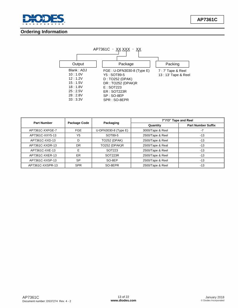
Ordering Information
AP7361C – XX XXX – XX
Output Package Packing
Blank : ADJ
10 : 1.0V
12 : 1.2V
15 : 1.5V
18 : 1.8V
25 : 2.5V
28 : 2.8V
33 : 3.3V
FGE : U-DFN3030-8 (Type E)
Y5 : SOT89-5
D : TO252 (DPAK)
DR : TO252 (DPAK)R
E : SOT223
ER : SOT223R
SP : SO-8EP
SPR : SO-8EPR
7 : 7' Tape & Reel
13 : 13' Tape & Reel
Part Number Package Code Packaging 7”/13” Tape and Reel
Quantity Part Number Suffix
AP7361C-XXFGE-7 FGE U-DFN3030-8 (Type E) 3000/Tape & Reel -7
AP7361C-XXY5-13 Y5 SOT89-5 2500/Tape & Reel -13
AP7361C-XXD-13 D TO252 (DPAK) 2500/Tape & Reel -13
AP7361C-XXDR-13 DR TO252 (DPAK)R 2500/Tape & Real -13
AP7361C-XXE-13 E SOT223 2500/Tape & Reel -13
AP7361C-XXER-13 ER SOT223R 2500/Tape & Reel -13
AP7361C-XXSP-13 SP SO-8EP 2500/Tape & Reel -13
AP7361C-XXSPR-13 SPR SO-8EPR 2500/Tape & Reel -13

AP7361C Document number: DS37274 Rev. 4 - 2
14 of 22 www.diodes.com
January 2018 © Diodes Incorporated
AP7361C
AD
VA
NC
E IN
FO
RM
AT
IO
N
NE
W P
RO
DU
CT
Marking Information
(1) U-DFN3030-8 (Type E)
XX : Identification Code( Top View )
X : Internal Code
XY
X X
W
Y : Year : 0~9 W : Week : A~Z : 1~26 week;
a~z : 27~52 week; z represents52 and 53 week
Device Package Identification Code
AP7361C-ADJ U-DFN3030-8 (Type E) SH
AP7361C-10 U-DFN3030-8 (Type E) SJ
AP7361C-12 U-DFN3030-8 (Type E) SK
AP7361C-15 U-DFN3030-8 (Type E) SV
AP7361C-18 U-DFN3030-8 (Type E) SW
AP7361C-25 U-DFN3030-8 (Type E) SX
AP7361C-28 U-DFN3030-8 (Type E) SY
AP7361C-33 U-DFN3030-8 (Type E) SZ
(2) SOT89-5
1 2 3
5 74
(Top View)
XX Y W X
Y : Year : 0~9W : Week : A~Z : 1~26 week;
X : Internal Code
a~z : 27~52 week;z represents 52 and 53 week
XX : Identification Code
Device Package Identification Code
AP7361C-ADJ SOT89-5 KR
AP7361C-10 SOT89-5 KS
AP7361C-12 SOT89-5 KT
AP7361C-15 SOT89-5 KU
AP7361C-18 SOT89-5 KV
AP7361C-25 SOT89-5 KW
AP7361C-28 SOT89-5 KX
AP7361C-33 SOT89-5 KZ

AP7361C Document number: DS37274 Rev. 4 - 2
15 of 22 www.diodes.com
January 2018 © Diodes Incorporated
AP7361C
AD
VA
NC
E IN
FO
RM
AT
IO
N
NE
W P
RO
DU
CT
Marking Information (Cont.)
(3) TO252 (DPAK)
Pin 1: IN, Pin 2: GND, Pin 3: OUT
61-VV
( Top View )
YY WW X X
Logo
Part Number
61-VV : 10 for 1.0V
12 for 1.2V
15 for 1.5V
18 for 1.8V
25 for 2.5V
28 for 2.8V
33 for 3.3V
X X : Internal Code
WW : Week : 01~52, 52 represents
YY : Year : 01~09
52 and 53 week
(4) SOT223
Pin 1: IN, Pin 2: GND, Pin 3: OUT
Y W X
61-VV
Logo
X : Internal code
( Top View )
Y : Year : 0~9W : Week : A~Z : 1~26 week;
a~z : 27~52 week; z repersents 52 and 53 week
Part Number
61-VV : 10 for 1.0V
12 for 1.2V
15 for 1.5V
18 for 1.8V
25 for 2.5V
28 for 2.8V
33 for 3.3V
(5) SOT223R
Pin 1: GND, Pin 2: OUT, Pin 3: IN
Y W X
61R-VV
Logo
X : Internal code
( Top View )
Y : Year : 0~9W : Week : A~Z : 1~26 week;
a~z : 27~52 week; z repersents 52 and 53 week
Part Number
61R-VV : 10 for 1.0V
12 for 1.2V
15 for 1.5V
18 for 1.8V
25 for 2.5V
28 for 2.8V
33 for 3.3V

AP7361C Document number: DS37274 Rev. 4 - 2
16 of 22 www.diodes.com
January 2018 © Diodes Incorporated
AP7361C
AD
VA
NC
E IN
FO
RM
AT
IO
N
NE
W P
RO
DU
CT
Marking Information (Cont.)
(6) TO252 (DPAK)R
Pin 1: GND, Pin 2: OUT, Pin 3: IN
61R-VV
( Top View )
YY WW X X
Logo
Part Number
61R-VV : 10 for 1.0V
12 for 1.2V
15 for 1.5V
18 for 1.8V
25 for 2.5V
28 for 2.8V
33 for 3.3V
X X : Internal Code
WW : Week : 01~52, 52 represents
YY : Year : 01~09
52 and 53 week
(7) SO-8EP
Pin 1: OUT, Pin 2: EN, Pins 3, 5, 6 and 7: NC, Pin 4: GND, Pin 8: IN
AP7361C-VV
( Top View )
YY WW X X E
Logo
Part Number
AP7361C-VV:
10 for 1.0V
12 for 1.2V
15 for 1.5V
18 for 1.8V
25 for 2.5V
28 for 2.8V
33 for 3.3V
SO-8EP
WW : Week : 01~52, 52 represents
YY : Year : 08, 09. 10~
52 and 53 week X X : Internal Code
1 4
8 5
(8) SO-8EPR
Pin 1: OUT, Pin 2: ADJ/NC, Pin 3: GND, Pins 4, 6 and 7: NC, Pin 5: EN, Pin 8: IN
7361CR-VV
( Top View )
YY WW X X E
Logo
Part Number
7361CR-VV:
Blank for ADJ
10 for 1.0V
12 for 1.2V
15 for 1.5V
18 for 1.8V
25 for 2.5V
28 for 2.8V
33 for 3.3V
SO-8EP
WW : Week : 01~52, 52 represents
YY : Year : 08, 09. 10~
52 and 53 week X X : Internal Code
1 4
8 5

AP7361C Document number: DS37274 Rev. 4 - 2
17 of 22 www.diodes.com
January 2018 © Diodes Incorporated
AP7361C
AD
VA
NC
E IN
FO
RM
AT
IO
N
NE
W P
RO
DU
CT
Package Outline Dimensions (All dimensions in mm.)
Please see http://www.diodes.com/package-outlines.html for the latest version.
(1) Package Type: U-DFN3030-8 (Type E)
(2) Package Type: SOT89-5
EH
D1
B1B
e
C
L
A
D
8° (4x)
R0.
200
L
U-DFN3030-8 Type E
Dim Min Max Typ
A 0.57 0.63 0.60
A1 0 0.05 0.02
A3 0.15
b 0.20 0.30 0.25
D 2.95 3.05 3.00
D2 2.15 2.35 2.25
E 2.95 3.05 3.00
e 0.65
E2 1.40 1.60 1.50
L 0.30 0.60 0.45
Z 0.40
All Dimensions in mm
SOT89-5
Dim Min Max Typ
A 1.40 1.60 1.50
B 0.50 0.62 0.56
B1 0.44 0.54 0.48
C 0.35 0.43 0.38
D 4.40 4.60 4.50
D1 1.62 1.83 1.733
E 2.40 2.60 2.50
e - - 1.50
H 3.95 4.25 4.10
L 0.65 0.95 0.80
All Dimensions in mm
b (x8)e
L (x8)
A1
A3
Z (x4)
D
D2
E2E
A

AP7361C Document number: DS37274 Rev. 4 - 2
18 of 22 www.diodes.com
January 2018 © Diodes Incorporated
AP7361C
AD
VA
NC
E IN
FO
RM
AT
IO
N
NE
W P
RO
DU
CT
Package Outline Dimensions (Cont.) (All dimensions in mm.)
Please see http://www.diodes.com/package-outlines.html for the latest version.
(3) Package Type: TO252 (DPAK)
b3
E
L3
D
L4
b2(2x)
b(3x)e
c
A
7° ± 1°
H
Seating Plane
A1
Gauge Plane
a
0.508
L
2.74REF
D1
A2
E1
TO252 (DPAK)
Dim Min Max Typ
A 2.19 2.39 2.29
A1 0.00 0.13 0.08
A2 0.97 1.17 1.07
b 0.64 0.88 0.783
b2 0.76 1.14 0.95
b3 5.21 5.46 5.33
c 0.45 0.58 0.531
D 6.00 6.20 6.10
D1 5.21 - -
e - - 2.286
E 6.45 6.70 6.58
E1 4.32 - -
H 9.40 10.41 9.91
L 1.40 1.78 1.59
L3 0.88 1.27 1.08
L4 0.64 1.02 0.83
a 0° 10° -
All Dimensions in mm

AP7361C Document number: DS37274 Rev. 4 - 2
19 of 22 www.diodes.com
January 2018 © Diodes Incorporated
AP7361C
AD
VA
NC
E IN
FO
RM
AT
IO
N
NE
W P
RO
DU
CT
Package Outline Dimensions (Cont.) (All dimensions in mm.)
Please see http://www.diodes.com/package-outlines.html for the latest version.
(4) Package Type: SOT223
(5) Package Type: SO-8EP
A1A
7°
7°
D
b
e
e1
b1C
E1
L
0°-10°
Q
E
0.25
Seating
Plane
Gauge
Plane
1
b
e
E1
A
A1
9° (All side)
4°±
3°
C
Q
N 45°
R 0.1
7°
D
E0
E
L
Seating Plane
Gauge Plane
F
H
EXPOSED PAD
SOT223
Dim Min Max Typ
A 1.55 1.65 1.60
A1 0.010 0.15 0.05
b 0.60 0.80 0.70
b1 2.90 3.10 3.00
C 0.20 0.30 0.25
D 6.45 6.55 6.50
E 3.45 3.55 3.50
E1 6.90 7.10 7.00
e - - 4.60
e1 - - 2.30
L 0.85 1.05 0.95
Q 0.84 0.94 0.89
All Dimensions in mm
SO-8EP
Dim Min Max Typ
A 1.40 1.50 1.45
A1 0.00 0.13 -
b 0.30 0.50 0.40
C 0.15 0.25 0.20
D 4.85 4.95 4.90
E 3.80 3.90 3.85
E0 3.85 3.95 3.90
E1 5.90 6.10 6.00
e - - 1.27
F 2.75 3.35 3.05
H 2.11 2.71 2.41
L 0.62 0.82 0.72
N - - 0.35
Q 0.60 0.70 0.65
All Dimensions in mm

AP7361C Document number: DS37274 Rev. 4 - 2
20 of 22 www.diodes.com
January 2018 © Diodes Incorporated
AP7361C
AD
VA
NC
E IN
FO
RM
AT
IO
N
NE
W P
RO
DU
CT
Suggested Pad Layout
Please see http://www.diodes.com/package-outlines.html for the latest version.
(1) Package Type: U-DFN3030-8 (Type E)
(2) Package Type: SOT89-5
(3) Package Type: TO252 (DPAK)
X3
X
Y
Y3
X1
X2
C
Y2Y1
C1
X1
X
Y2
Y1
Y
C
Dimensions Value (in mm)
C 0.65
C1 2.35
X 0.30
Y 0.65
Y1 1.60
Y2 2.75
Dimensions Value
(in mm)
C 1.500
C1 1.050
X 0.680
X1 0.760
X2 1.930
X3 3.680
Y 1.200
Y1 1.200
Y2 4.250
Y3 4.500
Dimensions Value (in mm)
C 4.572
X 1.060
X1 5.632
Y 2.600
Y1 5.700
Y2 10.700
Y(x8)
X (x8) C
C1
Y1 Y2

AP7361C Document number: DS37274 Rev. 4 - 2
21 of 22 www.diodes.com
January 2018 © Diodes Incorporated
AP7361C
AD
VA
NC
E IN
FO
RM
AT
IO
N
NE
W P
RO
DU
CT
Suggested Pad Layout (Cont.)
Please see http://www.diodes.com/package-outlines.html for the latest version.
(4) Package Type: SOT223
(5) Package Type: SO-8EP
Dimensions Value (in mm)
C 2.30
C1 6.40
X 1.20
X1 3.30
Y 1.60
Y1 1.60
Y2 8.00
Dimensions Value
(in mm)
C 1.270
X 0.802
X1 3.502
X2 4.612
Y 1.505
Y1 2.613
Y2 6.500
X1
Y1
Y
X C
C1 Y2
C
Y1
X1
X
Y
Y2
X2

AP7361C Document number: DS37274 Rev. 4 - 2
22 of 22 www.diodes.com
January 2018 © Diodes Incorporated
AP7361C
AD
VA
NC
E IN
FO
RM
AT
IO
N
NE
W P
RO
DU
CT
IMPORTANT NOTICE DIODES INCORPORATED MAKES NO WARRANTY OF ANY KIND, EXPRESS OR IMPLIED, WITH REGARDS TO THIS DOCUMENT, INCLUDING, BUT NOT LIMITED TO, THE IMPLIED WARRANTIES OF MERCHANTABILITY AND FITNESS FOR A PARTICULAR PURPOSE (AND THEIR EQUIVALENTS UNDER THE LAWS OF ANY JURISDICTION). Diodes Incorporated and its subsidiaries reserve the right to make modifications, enhancements, improvements, corrections or other changes without further notice to this document and any product described herein. Diodes Incorporated does not assume any liability arising out of the application or use of this document or any product described herein; neither does Diodes Incorporated convey any license under its patent or trademark rights, nor the rights of others. Any Customer or user of this document or products described herein in such applications shall assume all risks of such use and will agree to hold Diodes Incorporated and all the companies whose products are represented on Diodes Incorporated website, harmless against all damages. Diodes Incorporated does not warrant or accept any liability whatsoever in respect of any products purchased through unauthorized sales channel. Should Customers purchase or use Diodes Incorporated products for any unintended or unauthorized application, Customers shall indemnify and hold Diodes Incorporated and its representatives harmless against all claims, damages, expenses, and attorney fees arising out of, directly or indirectly, any claim of personal injury or death associated with such unintended or unauthorized application. Products described herein may be covered by one or more United States, international or foreign patents pending. Product names and markings noted herein may also be covered by one or more United States, international or foreign trademarks. This document is written in English but may be translated into multiple languages for reference. Only the English version of this document is the final and determinative format released by Diodes Incorporated.
LIFE SUPPORT Diodes Incorporated products are specifically not authorized for use as critical components in life support devices or systems without the express written approval of the Chief Executive Officer of Diodes Incorporated. As used herein: A. Life support devices or systems are devices or systems which: 1. are intended to implant into the body, or
2. support or sustain life and whose failure to perform when properly used in accordance with instructions for use provided in the labeling can be reasonably expected to result in significant injury to the user.
B. A critical component is any component in a life support device or system whose failure to perform can be reasonably expected to cause the failure of the life support device or to affect its safety or effectiveness. Customers represent that they have all necessary expertise in the safety and regulatory ramifications of their life support devices or systems, and acknowledge and agree that they are solely responsible for all legal, regulatory and safety-related requirements concerning their products and any use of Diodes Incorporated products in such safety-critical, life support devices or systems, notwithstanding any devices- or systems-related information or support that may be provided by Diodes Incorporated. Further, Customers must fully indemnify Diodes Incorporated and its representatives against any damages arising out of the use of Diodes Incorporated products in such safety-critical, life support devices or systems. Copyright © 2018, Diodes Incorporated www.diodes.com
![New Farnell | Electronic Component Distributors - Dimensions: [mm] … · 2019. 11. 13. · REV 5 V ESD Threshold/ Human Body Model V ESD HBM 2000 V Junction Temperature T ... 0603](https://img.pdfslide.us/doc/110x75/603f1b759a7ea2096a0eef2f/new-farnell-electronic-component-distributors-dimensions-mm-2019-11-13.jpg)