Embed Size (px)
Citation preview
ABCDEFG
UNIVERSITY OF OULU P .O. B 00 F I -90014 UNIVERSITY OF OULU FINLAND
A C T A U N I V E R S I T A T I S O U L U E N S I S
S E R I E S E D I T O R S
SCIENTIAE RERUM NATURALIUM
HUMANIORA
TECHNICA
MEDICA
SCIENTIAE RERUM SOCIALIUM
SCRIPTA ACADEMICA
OECONOMICA
EDITOR IN CHIEF
PUBLICATIONS EDITOR
Professor Esa Hohtola
University Lecturer Santeri Palviainen
Postgraduate research fellow Sanna Taskila
Professor Olli Vuolteenaho
University Lecturer Hannu Heikkinen
Director Sinikka Eskelinen
Professor Jari Juga
Professor Olli Vuolteenaho
Publications Editor Kirsti Nurkkala
ISBN 978-952-62-0207-5 (Paperback)ISBN 978-952-62-0208-2 (PDF)ISSN 0355-3213 (Print)ISSN 1796-2226 (Online)
U N I V E R S I TAT I S O U L U E N S I SACTAC
TECHNICA
U N I V E R S I TAT I S O U L U E N S I SACTAC
TECHNICA
OULU 2013
C 462
Jarmo Kukkola
GAS SENSORS BASED ON NANOSTRUCTURED TUNGSTEN OXIDES
UNIVERSITY OF OULU GRADUATE SCHOOL;UNIVERSITY OF OULU,FACULTY OF TECHNOLOGY,DEPARTMENT OF ELECTRICAL ENGINEERING;INFOTECH OULU
C 462
ACTA
Jarmo K
ukkola
C462etukansi.fm Page 1 Tuesday, September 3, 2013 12:19 PM

A C T A U N I V E R S I T A T I S O U L U E N S I SC Te c h n i c a 4 6 2
JARMO KUKKOLA
GAS SENSORS BASED ON NANOSTRUCTUREDTUNGSTEN OXIDES
Academic dissertation to be presented with the assent ofthe Doctoral Training Committee of Technology andNatural Sciences of the University of Oulu for publicdefence in OP-sali (Auditorium L10), Linnanmaa, on 27September 2013, at 12 noon
UNIVERSITY OF OULU, OULU 2013
Copyright © 2013Acta Univ. Oul. C 462, 2013
Supervised byProfessor Krisztián KordásProfessor Heli Jantunen
Reviewed byProfessor Thomas WågbergDocent Eeva-Liisa Lakomaa
ISBN 978-952-62-0207-5 (Paperback)ISBN 978-952-62-0208-2 (PDF)
ISSN 0355-3213 (Printed)ISSN 1796-2226 (Online)
Cover DesignRaimo Ahonen
JUVENES PRINTTAMPERE 2013
Kukkola, Jarmo, Gas sensors based on nanostructured tungsten oxides. University of Oulu Graduate School; University of Oulu, Faculty of Technology, Department ofElectrical Engineering; Infotech OuluActa Univ. Oul. C 462, 2013University of Oulu, P.O. Box 8000, FI-90014 University of Oulu, Finland
Abstract
The aim of this thesis is to study whether nanostructured particles of WO3 could be competitivecounterparts of traditional, more bulky materials in resistive gas sensor applications. Pristine andvarious surface decorated derivatives of three different types of WO3 nanoparticles applied on thesurface of lithographically defined Si chips were used in the work to analyse the electricalbehaviour of thin films when exposed to different gas atmospheres.
Nanosized particles of WO3, obtained by capillary force-induced collapse of porous anodictungsten oxide in water, were demonstrated as a sensing medium for the detection of H2 and NOanalytes. Commercially available nanoparticles of WO3 were also studied. After decorating theirsurface with metal/metal oxide nanoparticles (Ag, PdOx and PtOx), stable aqueous dispersionswere made and used for the inkjet printing of conductive patterns on test chips. Surface decorationwas found to affect substantially the gas response behaviour of the materials with the largestdifferences in response to H2 and NO. The third type of tungsten oxide applied consisted ofhydrothermally synthesized nanowires that were also surface decorated with PdO as well as withPtOx. The nanowires were suspended in water and drop cast on test chips for gas sensingmeasurements. The nanowire based devices allowed ultrasensitive detection of H2 even at roomtemperature.
The results summarized in this thesis indicate that resistive gas sensors based onnanostructured tungsten oxides are excellent alternatives to existing devices utilizing porous thickfilms or bulky thin films. Their high sensitivity, low operating temperature and low electricalpower consumption may enable the construction of portable sensors, for example by inkjetprinting, thus having great potential for fast prototyping but also for large scale production at lowcost.
Keywords: anodization, gas sensors, hydrogen, metal oxide, nanoparticles, nanowires,nitric oxide, printed electronics, tungsten oxide

Kukkola, Jarmo, Nanorakenteiset volframioksidiset kaasusensorit. Oulun yliopiston tutkijakoulu; Oulun yliopisto, Teknillinen tiedekunta, Sähkötekniikan osasto;Infotech OuluActa Univ. Oul. C 462, 2013Oulun yliopisto, PL 8000, 90014 Oulun yliopisto
Tiivistelmä
Väitöstyön tavoitteena on tutkia nanorakenteisten WO3 hiukkasten kilpailukykyä suhteessaperinteisiin suuremman kidekoon materiaaleihin resistiivisissä kaasusensorisovelluksissa. Työs-sä tutkittiin kolmella eri tekniikalla valmistettujen WO3 nanopartikkeleiden alkuperäisistä ja pin-takäsitellyistä versioista muodostettujen ohutkalvojen sähköisiä ominaisuuksia erilaisten kaasu-kehien funktiona.
Veden kapillaarivoimien aikaan saaman huokoisen anodisen volframioksidirakenteen romah-duksen kautta saatujen WO3 nanopartikkeleiden osoitettiin toimivan havaintoväliaineena H2 jaNO kaasuille. Myös kaupallisia WO3 nanopartikkeleita tutkittiin. Partikkelien pinta päällystettiinmetalli- ja metallioksidinanopartikkeleilla (Ag, PdOx and PtOx), jonka jälkeen niistä muodostet-tiin vakaita vesipohjaisia seoksia johtavien kuvioiden mustesuihkutulostukseen testisubstraateil-le. Pintakäsittelyn havaittiin vaikuttavan merkittävästi materiaalien kaasuvasteisiin erityisestiH2:n ja NO:n tapauksessa. Kolmannen tyyppinen väitöskirjassa tutkittu volframioksidimateriaa-li koostuu hydrotermisesti syntetisoiduista nanojohdoista, jotka ovat pintakäsitelty PdO tai PtOxnanopartikkeleilla. Nanojohdot sekoitettiin veteen ja pipetoitiin testisubstraateille kaasumittauk-sia varten. Tämän tyyppiset kaasusensorit olivat erityisen herkkiä H2 kaasulle jopa huoneenläm-mössä.
Väistökirjan tulosten mukaan nanorakenteiset volframioksidimateriaalit ovat erinomainenvaihtoehto perinteisille huokoisille paksukalvoille ja suhteellisen paksuille ohutkalvoille kaasu-sensorisovelluksissa. Niiden suuri herkkyys, alhainen toimintalämpötila ja matala sähkönkulu-tus voivat mahdollistaa kannettavien kaasusensorien valmistuksen, esimerkiksi mustesuihkutek-nologilla, nopeaan testaukseen ja suuren mittakaavan tuotantoon alhaisin kustannuksin.
Asiasanat: anodisointi, kaasuanturit, metallioksidi, nanohiukkaset, nanojohdot,painettava elektroniikka, typpioksidi, vety, volframioksidi

7
Acknowledgements
This work was done at the Microelectronics and Materials Physics Laboratories
of the University of Oulu in the framework of Segase, Rocaname, and Intag
projects.
I would like to thank my supervisor Prof. Krisztián Kordás for giving me the
opportunity and resources to carry out my research. His help was crucial in
numerous ways for the success of my work. Also, I am grateful to the staff of the
Microelectronics and Materials Physics Laboratories and to our collaborators for
their gratuitous help and guidance. In particular, the help of Dr. Andrei
Shchukarev, Anne-Riikka Leino, Jani Mäklin, Niina Halonen and Dr. Melinda
Mohl was critical on my journey. In addition, I want to acknowledge Prof.
Thomas Wågberg and Doc. Eeva-Liisa Lakomaa for acting as official reviewers
for this thesis and Professor Arthur Hill for revising the language of the thesis.
The financial support by the Graduate School of Infotech Oulu, the Riitta and
Jorma J. Takanen, Tauno Tönning and the Emil Aaltonen foundations is
acknowledged.
I would like to express my deepest gratitude to my wife Alemtsehay for her
unconditional love and understanding. In addition, I want to thank my son,
Joonatan, for making me smile every time I arrive at home after long day of work.
Oulu, June 2013 Jarmo Kukkola

8

9
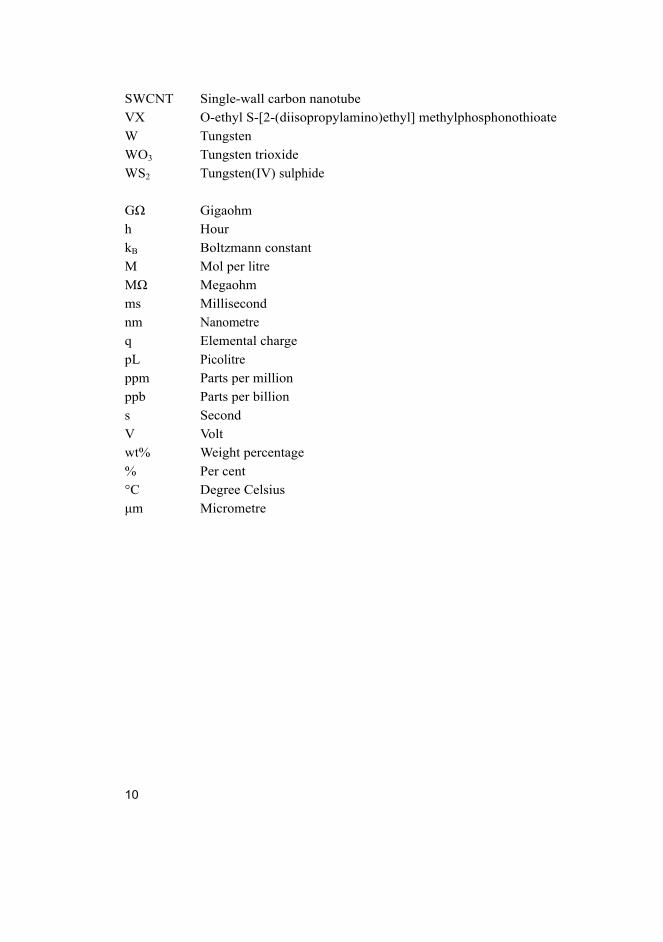
List of symbols and abbreviations
FESEM Field emission scanning electron microscopy
EDX Energy-dispersive X-ray spectroscopy
EFTEM Energy filtered transmission electron microscopy
HRTEM High resolution transmission electron microscopy
Ld Debye length
n Density of electrons
T Temperature
TEM Transmission electron microscopy
UV Ultraviolet
XPS X-ray photoelectron spectroscopy
XRD X-ray diffraction
εr Relative permittivity
ε0 Vacuum permittivity
Ag Silver
AgNO3 Silver nitrate
Ar Argon
AAO Anodic aluminium oxide
CH4 Methane
CO Carbon monoxide
HCl Hydrochloric acid
H2 Hydrogen
H2S Hydrogen sulphide
NaF Sodium fluoride
Na2O4W Sodium tungstate
Na2SO4 Sodium sulphate
NO Nitric oxide
O2 Oxygen
PdO Palladium oxide
Pd(C5H7O2)2 Palladium acetylacetonate
Pt Platinum
PtOx Platinum oxide/metal
Pt(C5H7O2)2 Platinum acetylacetonate
Si Silicon
SiO2 Silicon dioxide
10
SWCNT Single-wall carbon nanotube
VX O-ethyl S-[2-(diisopropylamino)ethyl] methylphosphonothioate
W Tungsten
WO3 Tungsten trioxide
WS2 Tungsten(IV) sulphide
GΩ Gigaohm
h Hour
kB Boltzmann constant
M Mol per litre
MΩ Megaohm
ms Millisecond
nm Nanometre
q Elemental charge
pL Picolitre
ppm Parts per million
ppb Parts per billion
s Second
V Volt
wt% Weight percentage
% Per cent
°C Degree Celsius
μm Micrometre
11
List of original papers
This thesis consists of an overview and the following four publications:
I Kukkola J, Mäklin J, Halonen N, Kyllönen T, Tóth G, Szabó M, Shchukarev A, Mikkola JP, Jantunen H & Kordás K (2010) Gas sensors based on anodic tungsten oxide. Sensors and Actuators B 153(2): 293–300.
II Kukkola J, Mohl M, Leino AR, Tóth G, Wu MC, Shchukarev A, Popov A, Mikkola JP, Lauri J, Riihimäki M, Lappalainen J, Jantunen H & Kordás K (2012) Inkjet-printed gas sensors: metal decorated WO3 nanoparticles and their gas sensing properties. Journal of Materials Chemistry 22(34): 17878–17886.
III Kukkola J, Mohl M, Leino AR, Mäklin J, Halonen N, Shchukarev A, Konya Z, Jantunen H & Kordás K (2013) Room temperature hydrogen sensors based on metal decorated WO3 nanowires. Sensors and Actuators B 186: 90–95.
IV Kukkola J, Rautio A, Sala G, Pino F, Tóth G, Leino AR, Mäklin J, Jantunen H, Uusimäki A, Kordás K, Gracia E, Terrones M, Shchukarev A & Mikkola JP (2010) Electrical transport through single-wall carbon nanotube-anodic aluminum oxide-aluminum heterostructures. Nanotechnology 21(3): 035707(1–6).
Paper I describes the preparation and gas response behaviour of anodic WO3
based gas sensors. The formation of nanoporous WO3 material was achieved by
anodizing W metal foils in NaF electrolyte and stripping off the formed anodic
oxide by wetting the surface with water. After collection, the obtained dispersion
was drop cast over Si/SiO2 substrates with Pt-electrodes. The dried WO3 layers
were tested as resistive gas sensing elements for detection of CO, H2, NO and O2
at temperatures ranging from 20 to 270 °C.
In Paper II, commercial WO3 nanoparticles with size less than 100 nm were
decorated with Ag, PdOx and PtOx nanoparticles with diameters ranging from 1 to
5 nm. After suspending the prepared materials in deionized water, the dispersions
were inkjet printed on Si/SiO2 substrates having microscopic Pt-electrodes.
Depending on the decorating metal or metal oxide nanoparticle, selective sensing
of H2 and NO analytes was demonstrated. The presented preparation method of
gas sensors by inkjet printing could be used in environmentally friendly mass
production of low cost metal oxide gas sensors.
Paper III describes gas sensors based on pristine, PdO and PtOx decorated
WO3 nanowires that were drop cast on Si/SiO2 substrates with Pt electrodes.
Nanowire based sensors were studied to see how they compared to nanoparticle
based counterparts discussed in Papers I and II. The prepared PdO and PtOx
decorated WO3 nanowire based gas detectors were shown to be applicable even
for room temperature sensing of H2.
12
Paper IV describes inkjet printing of carbon nanotubes on anodic aluminium
oxide substrates. This article serves as an example of a mass production capable
technique for conductive electrodes through inkjet printing.
Planning of the experiments, construction of the sensors, electrical
measurements and data processing were mostly contributed by the author. Test
chips used in the experiments were prepared by Niina Halonen. XRD and XPS
analyses were carried out by Anne-Riikka Leino and Dr. Andrey Shchukarev,
respectively. Teemu Kyllönen performed part of the anodic tungsten oxide
synthesis. Aatto Rautio prepared the anodic aluminium substrates. The pristine
WO3 nanowires were synthesized by Mária Szabó. Metal/metal oxide decoration
of WO3 nanoparticles and nanowires was carried out by Dr. Melinda Mohl. The
inkjet printing of carbon nanotubes in Paper IV was contributed by Giovanni Sala,
Flavio Pino and Dr. Eduardo Gracia. All measurement results were discussed and
evaluated together with the co-authors. The manuscripts were written with the
help of the co-authors.
13
Contents
Abstract
Tiivistelmä
Acknowledgements 7 List of symbols and abbreviations 9 List of original papers 11 Contents 13 1 Introduction 15
1.1 Gas sensing ............................................................................................. 15 1.2 Tungsten oxides ...................................................................................... 18 1.3 Objective and outline of thesis ................................................................ 22
2 Materials and methods 23 2.1 Device preparation .................................................................................. 23 2.2 Testing and measurements ...................................................................... 25
3 Results and discussion 27 3.1 Background of the used preparation methods ......................................... 27 3.2 Analysis of materials and deposition methods ........................................ 28 3.3 Gas sensing results .................................................................................. 36
4 Conclusions 45 References 47 Original papers 55

14
15
1 Introduction
A sensor is a device that converts physical or chemical stimuli to electric signals
(Kenny 2005). A gas sensor is a device that detects the presence or measures the
concentration of a particular atom, molecule or ion in an atmosphere. The term
chemical sensor covers devices (including also those that detect analytes in
liquids) whose operation is based on one or more chemical reactions (i.e. an
electron or proton transfer occurs) that take place while sensing the analyte.
1.1 Gas sensing
Atmospheric air contains a number of gaseous species (Table 1). However, there
are many natural and artificial gas sources that could alter the composition of the
local atmosphere. Some gases are vital for life, while others are harmful, even
deadly. The concentration of each gas should be maintained between safe upper
and lower specific for each type of gas. Even trace amount of some gases could
be dangerous to life; for example, nerve agent VX could be lethal at 20 ppb.
Contrarily, oxygen is only safe, when the concentration is around 20%. Control
over the local atmospheric conditions often requires a real-time feedback about its
composition that may be obtained with the help of gas sensors.
Table 1. Composition of dry air in close proximity to the Earth's surface (Barry &
Chorley 1992).
Type of gas Concentration (volume %)
Nitrogen 78.08
Oxygen 20.98
Argon 0.93
Carbon dioxide 0.035
Neon 0.0018
Methane 0.0017
Krypton 0.0011
Helium 0.0005
Hydrogen 0.00005
Ozone 0.00006
Xenon 0.00009
According to a global gas market survey executed in 2010, the value of the gas
sensor market was over 3.9 billion dollars in 2010 with a 5.9% annual growth rate
16
(BCC Research LLC 2010). Similarly, according to a global chemical sensors
market survey conducted in 2010, a greater than 17 billion dollar market for
chemical sensors is estimated by 2015 (Global Industry Analysts, Inc. 2010). In
another report, the chemical sensor market is expected to grow by up to 6 billion
dollars by 2014 in the US with an 8.6% annual growth rate (Freedonia Group,
Inc.). These reports indicate the growing interest in this already important field of
business. Industrial production, the medical field, environmental monitoring,
indoor air quality control, transportation and security control all have a growing
demand for better and cheaper gas sensors.
Probably the first gas alarm system developed was the use of canary birds as
an early warning mechanism in coal mines (Goodman 2004). One of the first
artificial gas detectors, Davy's lamp (1815), was designed to detect oxygen
deficiency or the presence of CH4 in coal mines (Simonin 1869). While some gas
sensors had been developed earlier for the use of professionals in limited fields,
the first products designed for consumer markets were launched around 1970
(Aswal & Gupta 2007) based on the works of Seiyama (Seiyama et al. 1962) and
Taguchi (Taguchi 1962) related to semiconducting electrochemical gas sensors.
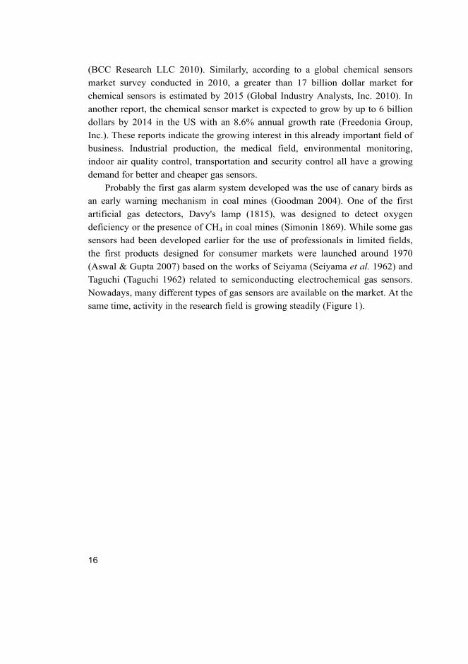
Nowadays, many different types of gas sensors are available on the market. At the
same time, activity in the research field is growing steadily (Figure 1).
17
Fig. 1. Number of publications found using keyword "gas sensor*" in Web of
Knowledge (academic citation indexing and search service). Search was conducted
on 10.10.2012.
Gas sensors can be divided into categories in several different ways. For instance,
there are passive and active sensors: passive sensors provide their own power, for
example through exothermic chemical reaction with an analyte, while active
devices need an external power source (Kenny 2005). Gaseous species are known
to modulate many physical and chemical properties of gas sensing materials,
enabling the exploitation of various working principles. A broad spectrum of solid
state (e.g. resistive), mass sensitive (e.g. surface acoustic wave) and optical
sensors (e.g. optical fibre) has been demonstrated during the past decades. Before
launching gas sensing products on to the market, manufacturers should accurately
characterize the specifications of their products such as sensitivity, analysis range,
selectivity, cross-sensitivity, stability, accuracy, resolution, linearity, response time,
lifetime, calibration frequency, cost, usability and tolerance to environmental
conditions. Because of the complexity of gas detection, it is often difficult to fulfil
all of the desired specifications satisfactorily. Common physical sensors, such as
pressure gauges or thermometers, measure only one parameter, but the case of
chemical sensors is much more complex. One of the main reasons for this is the
large number of existing chemical species, making it very difficult to selectively
detect each of them. In addition to the signal caused by the gases, it is common
for the output of the chemical sensors to depend on many other parameters, such
as temperature, presence and concentration of moisture, electromagnetic radiation,
gas sensing history, background gases, and contaminating particles. These factors
18
enhance the need for testing and slow down the market entry of chemical sensors.
Even though chemical sensors have been studied extensively, a universal device
that works in every gas sensing application does not yet exist. When choosing a
sensor for practical applications, the type of gases under analysis and the expected
environmental conditions should be taken into account. This thesis focuses on
resistive metal oxide sensors to be operated in air.
1.2 Tungsten oxides
Similar to all heavy elements, tungsten atoms were formed in massive stars
though energy consuming reactions (Lassner & Schubert 1999). At the time of its
discovery at the end of 18th century by Juan Jose and Fausto Elhuyar, tungsten
was named "wolfram", after the mineral in which it was found (Mahadi 2007).
However, the English name originates from the Swedish term "tung sten", which
can be directly translated as heavy stone (Krebs 2006). The original name is still
used in many other languages, such as Finnish, German, Russian and Spanish, and
we can see a reminder of the past in its chemical symbol, W. Tungsten is a hard
transition metal (in the group of refractories together with Nb, Ta, Mo and Re)
with the second highest melting point of all the elements. Reserves of the metal
are mainly in the forms of wolframite (Fe,Mn)WO4 and scheelite CaWO4 ores
(Lassner & Schubert 1999) in which tungsten is in its +6 oxidation state. However,
in various compounds tungsten may also have lower oxidation states such as +1 in
WH, +4 in WC, between +2 and +6 in halides, just to mention a few examples.
Over 70,000 tons of W was produced in the year 2011, with China as the
dominant player in the field (Shedd 2012).
WO3 orients in a number of different crystal forms at atmospheric pressure.
Below −43 °C monoclinic (ε-WO3), from −43 °C to −17 °C triclinic (δ-WO3),
from −17 °C to 330 °C monoclinic (γ-WO3), from 330 °C to 740 °C orthorhombic
(β-WO3) and above 740 °C tetragonal (α-WO3) phases are the thermodynamically
stable ones. It is worth mentioning that the phase transition temperatures are
lower in nanocrystalline WO3 (Zheng et al. 2011). WO3 is an n-type
semiconductor with a band gap from 2.6 eV in crystalline to 3.3 eV in amorphous
materials (Carpenter et al. 2012). As with other semiconductors, an increasing
bandgap has been observed with reducing grain size (Gullapalli et al. 2010).
Normally the electronic band structure is modified by common oxygen
deficiencies in the lattice leading to increased conductivity (Dixon et al. 1998).
19
In the middle of the 19th century, R. Oxland patented a method for producing
Na2O4W, WO3 and W (British patent 11848, 1847). One of the first synthesis
methods of nanostructured WO3 was performed by a sol-gel route (Judeinstein &
Livage 1991). Recently, several competing techniques for synthesizing
nanostructured WO3 have been introduced such as gas evaporation (Lin et al. 1994), flame pyrolysis (Hoang-Van & Zegaoui 1995), RF magnetron sputtering
(Pyun et al. 1996), template assisted growth (Lakshmi et al. 1997), wet chemical
deposition (Krings & Talen 1998), thermal evaporation (Zhu et al. 1999), electron
beam evaporation (Greenwood 1999), electrodeposition (Shen et al. 2000), pulsed
laser deposition (Zhao et al. 2000), spray pyrolysis (Regragui et al. 2000), anodic
oxidation (Mukherjee et al. 2003), hydrothermal (Lou & Zeng 2003), and arc
discharge (Guo 2005). The wide spectrum of preparation methods found in the
literature indicates the extensive interest in the topic.
WO3 has been used in many other applications, for example electrochromic
films (Deb 1969), photocatalytic surfaces (Lyashenko & Gorokhovatskii 1975),
photoelectrochemical electrodes (Quarto et al. 1985), battery electrodes (Pereira-
Ramos et al. 1993), field emitters (Gotoh et al. 1993), thermoelectric devices
(Polaczek et al. 1994), thermochromic films (Durrani et al. 2002), optical
recording media (Aoki et al. 2005), superconductors (Reich et al. 2009), solar cell
electrodes (Zheng et al. 2010), and gas sensors (Zheng et al. 2011). The first WO3
based gas sensor was reported in 1967 (Shaver 1967).
Gas sensing by metal oxides is based on several distinct phenomena such as
surface adsorption and desorption, reactions on surfaces, diffusion of gases in a
porous membrane and inside the crystal lattice (Korotcenkov 2005). Until the rise
of nanotechnology, resistive metal oxide sensors were made of relatively large
particles by thick film technologies. During the recent decades, it was understood
that nanostructured thin films have many advantages over traditional thick films
based on microscopic or more bulky particles/films. The sensitivity and the
response time could be enhanced, while the power consumption and the
manufacturing costs of devices could be reduced.
A good approximation of the optimal particle size for gas sensing
applications can be obtained by calculating the Debye length (Ld) in the particular
material.
= /( ) (1)
The Debye length is the scale over which the electrons screen out the local electric
field caused by dipoles. In the case of sensors, such an external field arises from
20
surface adsorbates that polarize the solid. In the optimal case, at least one
dimension of the gas sensing material is the scale of twice the Debye length, Ld,
when the whole bulk of the material can be affected by the electric fields. In WO3
materials, the carrier concentration and the relative permittivity have been
evaluated to be from 1023 to 1025 m-3 (Patel et al. 2009, Patil et al. 2000, Regragui
et al. 2001 & Yoon et al. 1997) and ~20 (Goodenough et al. 1984), respectively.
Based on these values the optimum crystal size, in at least one of the coordinates,
is between 4 to 40 nm (at 500 K), which has also been confirmed experimentally
(Tamaki et al. 1994).
As with other types of gas sensors, metal oxide based detectors are known to
be sensitive to many types of gases. This is a general problem, because the signal
from the background gases could disturb detection of the target analyte. Another
challenge to overcome is the cross-sensitivity, i.e. the alteration of a response for
a particular analyte caused by another analyte. In other words, the responses are
not orthogonal functions of various stimuli. However, there are some methods to
enhance the selectivity of metal oxide gas sensors. In practical applications, the
composition of the gas sensing metal oxide layers is commonly modified by other
metal or metal oxide additives in order to alter the gas responses, and preferably
to induce a more selective response for a particular stimulus. In principle, three
different kinds of modifications exist. One is lattice doping with impurities to
create new energy levels in the forbidden band near to the edges of valence and/or
conduction bands. The appearance of new impurity levels affect both the inter-
and intra-band carrier transport (Burstein 1954, Moss 1954, Niklasson &
Granqvist 2007), while alteration of the carrier concentration and mobility lead to
a change in Debye length. The other alternative is surface functionalization by
chemical groups to change terminal bonds and thus the chemical/adsorption
behaviour of the surface. This is an emerging field and at present is applied
mainly to carbon based sensors (Qi et al. 2003, Balasubramanian & Burghard
2005, Mäklin et al. 2007). The third approach is the surface decoration of the
semiconducting particles with metal and/or metal oxide nanoparticles, often
referred to in the literature as sensitization. Surface decoration may have multiple
effects on sensor operation. On the one hand, the immobilized metal and metal
oxide nanoparticles can create local Schottky and p-n junctions, respectively.
Both types of junctions cause a clear change in charge injection mechanisms
through the interfaces thus influencing carrier distribution after polarization or
electron/proton transfer caused by chemisorbed moieties or by chemical reactions
taking place on the surface. On the other hand, the decorating particles can very
21
selectively adsorb and/or react with particular analytes (e.g. Pd/PdO (Mubeen et al. 2007) and Pt (Kumar & Ramaprabhu 2006) with H2; Ag (Fam DWH et al. 2009) and Au (Mubeen S et al. 2010) with H2S; CeO2 (Manorama SV et al. 2003)
and Nb (Sharma et al. 1998) with O2; Ru (Niranjan et al. 2002) and Pd (Sengupta
et al. 2010) with hydrocarbons; AgO (Cui et al. 2012) and SnO2 (Mashock et al. 2012) with NH3; Al (Roy & Basu 2004) and Ru (Kim et al. 2012) with amines;
Au (Joshi et al. 2009), Pd/PdO (Chang et al. 2012) with CO and so forth) thus
making the sensors also selective towards the corresponding molecules. Therefore,
according to the reasons described above, it is of the utmost importance to choose
the right particle size and post-treatment to achieve reasonable sensor-analyte
pairs. In addition, the operation temperature has a huge impact on responses since
carrier densities, injection efficiencies, carrier mobility, and surface gas
adsorption/desorption as well as chemical reaction rates and many other processes
involved in sensing are also highly dependent on this parameter (typically
exponential dependencies!).
Gas sensor arrays can be used for more selective detection of gases. The idea
is to use several different types of sensors that measure gas responses in parallel.
All of the signals can be combined and interpreted for a better understanding of
the composition of the local atmosphere.
WO3 based sensors for detection of several types of gases have been
proposed; for example NO/NO2 (Akiyama et al. 1991), NH3 (Maekawa et al. 1992), H2 (Ito et al. 1993), CH3SH (Ando et al. 1994), Cl2 (Dawson & Williams
1996), humidity (Li & Tsai 1996), CO2 (Chiu & Tseung 1999), O3 (Qu &
Wlodarski 2000), CO (Fukuda et al. 2001), ethanol (Yu-De et al. 2001), volatile
organic compounds (Kanda & Maekawa 2005), and petroleum (Chaudhari et al. 2006). As can be seen here, WO3 can be sensitive to a vast number of different
types of gases, so researchers should be careful when interpreting the results from
gas sensing measurements. Unfortunately very few, if any, gas sensor research
works (including my own) have actually been executed by testing all of the gases
on the list above. It is practically impossible to study gas sensitivity to all the
gases and their mixtures because of the nearly infinite number of combinations of
parameters (temperature, gas concentrations, humidity, cross-sensitivity, etc.). If
gas sensors are used in practice, all the possible gases in the operation atmosphere
should be known and the applicability of the sensor in these conditions should be
verified to avoid spurious signals from untested background gases or their
combinations. Artificial neural networks (Hivert et al. 1995), linear discriminant
22
analysis and principal component analysis (Carrasco et al. 1998) have been used
for processing of response data of gas sensors to multi-component gas mixtures.
1.3 Objective and outline of thesis
The main objective of this thesis was to prepare, test and compare gas sensors
based upon different types of nanostructured tungsten oxides. The greatest
achievement of this work was to demonstrate a low cost technique that could be
applied in mass production of resistive gas sensing elements based on metal oxide
nanoparticles. To reach this goal, an inkjet printing method was developed for
preparing active gas sensing layers based on WO3 nanoparticles and their surface
decorated derivatives, and conductive electrodes made of carbon nanotubes.
Using these methods, entirely inkjet printed gas sensing components could be
produced with very few production steps. In this work, printing was demonstrated
only on Si, Si/SiO2 and AAO substrates. However, it is anticipated that the same
technique could be applied in almost any context.
In chapter 2, descriptions are given of the used materials and preparation
methods as well as characterization techniques for materials and device
performance.
Chapter 3 deals with the results and discussion of the experiments. A brief
history of the used device preparation techniques is provided, which is then
followed by the introduction of structural details of the tungsten oxide based
materials used and the corresponding sensor devices. Finally, the gas sensing
performance of each type of gas sensor is evaluated and discussed in the context
of possible surface adsorption/reaction mechanisms with the help of background
information collected from scientific literature.
In chapter 4, conclusions are given of the work performed for the thesis. The
prepared gas sensors are further compared with each other, together with a
discussion about the relevance of the work in the context of industrial mass
production.
23
2 Materials and methods
In this work, relatively similar resistive gas sensors are prepared with comparable
techniques, with the largest difference being in the preparation of the active gas
sensing nanomaterials. The composition and the performance of all of the
prepared sensors are studied by similar methods to enable reasonable comparison.
2.1 Device preparation
All the active gas sensing materials prepared during this research were based on
either nanoporous membrane/nanoparticles/nanowires of pristine or metal
decorated WO3. These sensing materials were deposited either by drop casting
(Papers I & III) or by inkjet printing (Paper II) on Si/SiO2 substrates having
platinum electrodes that allowed probing and subsequent electrical as well as gas
sensing analysis. All the prepared devices were dried overnight and heated before
the gas sensing measurements in order to desorb moisture and stabilize the
resistance of the sensors.
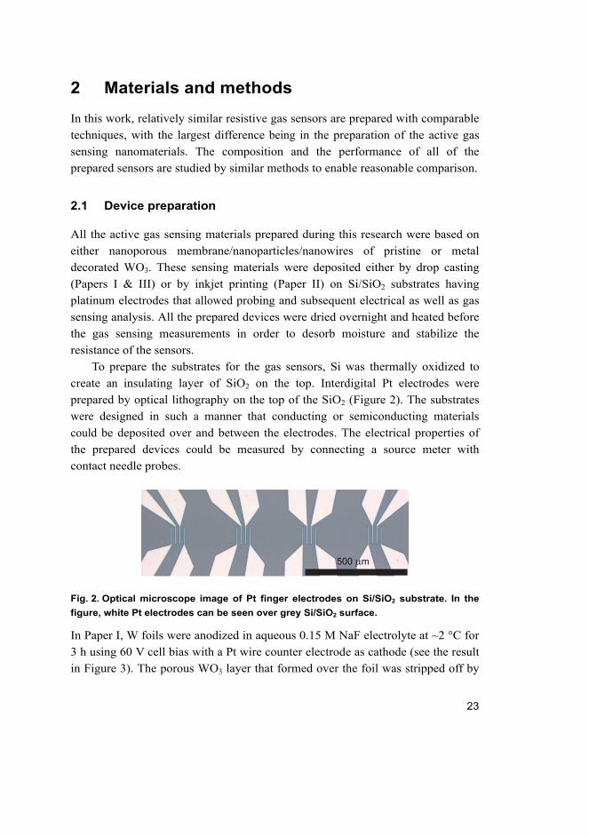
To prepare the substrates for the gas sensors, Si was thermally oxidized to
create an insulating layer of SiO2 on the top. Interdigital Pt electrodes were
prepared by optical lithography on the top of the SiO2 (Figure 2). The substrates
were designed in such a manner that conducting or semiconducting materials
could be deposited over and between the electrodes. The electrical properties of
the prepared devices could be measured by connecting a source meter with
contact needle probes.
Fig. 2. Optical microscope image of Pt finger electrodes on Si/SiO2 substrate. In the
figure, white Pt electrodes can be seen over grey Si/SiO2 surface.
In Paper I, W foils were anodized in aqueous 0.15 M NaF electrolyte at ~2 °C for
3 h using 60 V cell bias with a Pt wire counter electrode as cathode (see the result
in Figure 3). The porous WO3 layer that formed over the foil was stripped off by
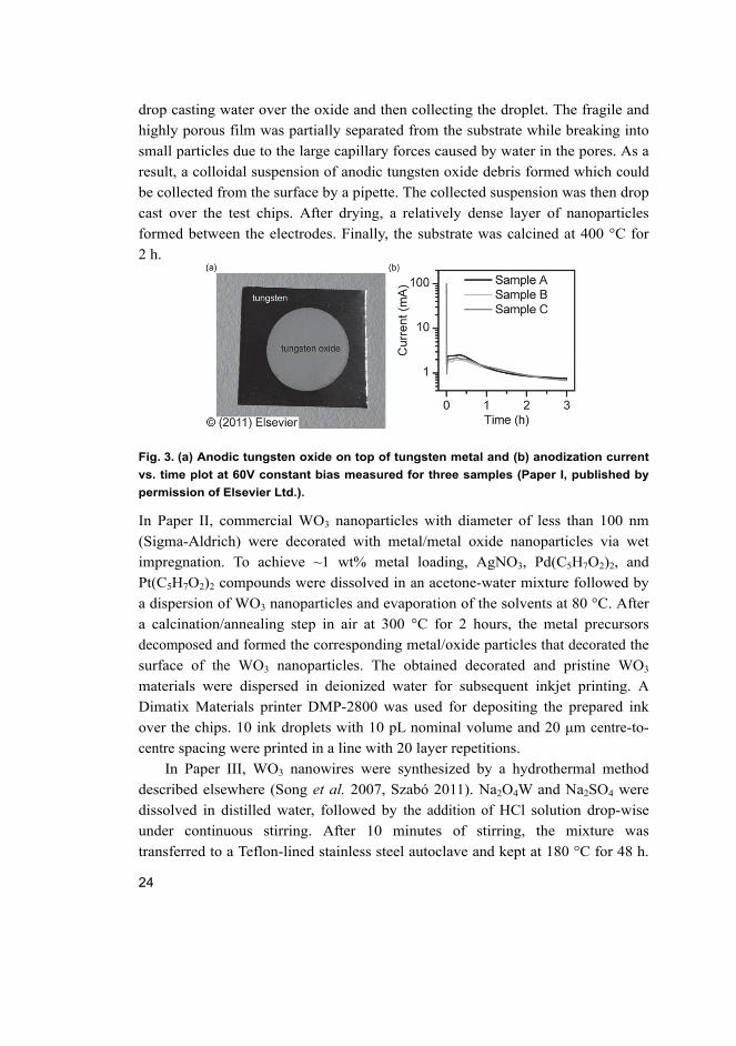
24
drop casting water over the oxide and then collecting the droplet. The fragile and
highly porous film was partially separated from the substrate while breaking into
small particles due to the large capillary forces caused by water in the pores. As a
result, a colloidal suspension of anodic tungsten oxide debris formed which could
be collected from the surface by a pipette. The collected suspension was then drop
cast over the test chips. After drying, a relatively dense layer of nanoparticles
formed between the electrodes. Finally, the substrate was calcined at 400 °C for
2 h.
Fig. 3. (a) Anodic tungsten oxide on top of tungsten metal and (b) anodization current
vs. time plot at 60V constant bias measured for three samples (Paper I, published by
permission of Elsevier Ltd.).
In Paper II, commercial WO3 nanoparticles with diameter of less than 100 nm
(Sigma-Aldrich) were decorated with metal/metal oxide nanoparticles via wet
impregnation. To achieve ~1 wt% metal loading, AgNO3, Pd(C5H7O2)2, and
Pt(C5H7O2)2 compounds were dissolved in an acetone-water mixture followed by
a dispersion of WO3 nanoparticles and evaporation of the solvents at 80 °C. After
a calcination/annealing step in air at 300 °C for 2 hours, the metal precursors
decomposed and formed the corresponding metal/oxide particles that decorated the
surface of the WO3 nanoparticles. The obtained decorated and pristine WO3
materials were dispersed in deionized water for subsequent inkjet printing. A
Dimatix Materials printer DMP-2800 was used for depositing the prepared ink
over the chips. 10 ink droplets with 10 pL nominal volume and 20 μm centre-to-
centre spacing were printed in a line with 20 layer repetitions.
In Paper III, WO3 nanowires were synthesized by a hydrothermal method
described elsewhere (Song et al. 2007, Szabó 2011). Na2O4W and Na2SO4 were
dissolved in distilled water, followed by the addition of HCl solution drop-wise
under continuous stirring. After 10 minutes of stirring, the mixture was
transferred to a Teflon-lined stainless steel autoclave and kept at 180 °C for 48 h.
25
The product was collected by centrifugation, washed with distilled water and
ethanol and finally dried at 60 °C in air so that pristine WO3 nanowires were
obtained. Some of the nanowires were then decorated with Pd or Pt nanoparticles
similarly to those described in Paper II. Samples of pristine, Pd and Pt decorated
nanowires were mixed with water and drop cast over the sensor test substrates.
In Paper IV, 2.0 mg of COOH-functionalized single-wall carbon nanotubes
(SWCNTs) were suspended in 15 ml of de-ionized water through ultrasonic
agitation for 3–5 h, followed by centrifugation to stabilize the dispersion. The
obtained suspension was relatively stable because COOH-functionalization
helped to increase the solubility of the nanotubes in water. The obtained
dispersion was inkjet printed on anodic aluminium oxide (AAO) substrates using
varying layer thicknesses to form areas with distinct sheet resistances. Square
shaped electrodes with 2 mm side were deposited with 25 μm drop spacing and
100 repeated layers to obtain low sheet resistances.
The samples were then tested and measured. X-ray photoelectron spectroscopy
(XPS, Kratos Axis Ultra, Al Kα source, analysis area 0.3 mm x 0.7 mm, applying
charge neutralizer) was used for analysis of each type of the prepared gas sensing
materials to measure the elemental composition and the oxidation states, while
energy-filtered transmission electron microscopy (EFTEM, Leo 912 Omega) and
field-emission scanning electron microscopy (FESEM, Zeiss ULTRA Plus) was
used to visualize micro- and nanoscopic structures. X-ray diffraction (XRD,
Philips PW 1380, Cu Kα radiation) enabled evaluation of the crystal structures
and the volume averaged diameters of the crystallites (diameter evaluation was
not performed in Paper I). XRD could only be used for characterizing the WO3
materials, not the decoration metals, due to the low proportion, the small size and
possibly the amorphous state of the added metals/oxides.
The gas sensing performance of the prepared devices was tested in a Linkam
THMS600 heating and freezing stage. Analyte gases (CH4, CO, H2, H2S, NO or
O2) were mixed with the background gas (synthetic air or argon) in a gas blender
before insertion into the test chamber. All the used gases had purity of 99.999%
(synthetic air, CH4, CO, H2, H2S, NO, O2) or 99.9999% (Ar) and were free of
moisture. Temperature and gas concentration were computer-controlled allowing
long, even >24 hour, measurement cycles. During the gas sensing measurements,
the resistance of the sensors was monitored by an Agilent 3458A multimeter
using constant bias. Sheet resistance in Paper IV was measured using a Keithley
2612 Sourcemeter.

26
27
3 Results and discussion
The results of this thesis are mainly focused on evaluation of the gas sensing
performance of various nanostructured WO3 based thin films. These results are
complemented by the evaluation of the structural and the elemental compositions
of the prepared materials with the help of FESEM, EFTEM/HRTEM, XRD and
XPS techniques.
3.1 Background of the used preparation methods
Oxidation of metallic tungsten through anodization has been known since the
beginning of the 20th century (Koerner 1917). Anodization (or electrochemical
etching) is a relatively simple method in which a metal in question (anode) and a
counter electrode (cathode) are submerged in a suitable electrolyte and then
biased to oxidize and partially dissolve the forming oxide layer in an
electrochemical reaction on the top surface of the anode material (Pap et al. 2005,
Kordás et al. 2006, Mor et al. 2006). Depending on the anodizing conditions,
such as the type of the metal and the electrolyte, applied voltage, temperature, and
duration of the process, different kinds of oxide structures can be formed. While
many works on anodic tungsten oxide appear in the literature, discussion about
the gas sensing applications is limited. In Paper I, the anodization technique is
used to synthesize the sensing material.
Even though nanoparticles are often considered as inventions of
contemporary science, their history can actually be traced back to the 9th century
in Mesopotamia, where nanoparticles were used in pottery to generate a glittering
effect (Sattler 2011). However, studying their composition was only possible after
the invention of electron microscopes in the 1930's. Metallic tungsten
nanoparticle powders were already being prepared in the 1960's (Lamprey &
Ripley 1961). One of the earliest studies about WO3 nanocrystals was published
more than twenty years ago (Judeinstein & Livage 1991). Since then, the research
activity in the field of WO3 nanoparticles has been growing rapidly.
Printed electronics started with patterning and reducing of silver salts to
create conducting wires on linen paper as suggested by Thomas Edison in 1904
(Carano et al. 2004). During the long history of printing technologies, many types
of printing techniques have been developed that can be divided into three main
groups: mass printing (flexography, gravure, and offset printing), sheet-fed
printing (inkjet and screen printing), and step-by-step printing (stamping, nano-
28
imprint, and UV-lithography) (Bensebaa F 2013). Screen printed metal oxide gas
sensors were already prepared by the beginning of the 1990's. Pioneer work in the
field was accomplished by scientists of our laboratory (Mizsei & Lantto 1991).
However, inkjet printed chemical sensors based on metal oxides is an emerging
technology (Lee et al. 2007). Not much has yet been published in the field
because of the young age of this printing method itself. Paper II, demonstrates
drop-on-demand inkjet printing of WO3 nanoparticles as it enables accurate
deposition of very small amounts of WO3 nanoparticles on wanted locations. In
Paper IV, a similar method is used for printing conductive electrodes based on
carbon nanotubes.
In the mainstream research for discovering one-dimensional materials
(motivated to a large extent by the exploration of the potential of carbon
nanotubes), enormous efforts have been placed on finding practical synthesis
routes as well as on exploiting the properties of metal oxide nanowires in various
innovative devices. Due to their large aspect ratio, one-dimensional materials
possess distinct properties compared to their corresponding nanoparticle or bulk
forms. In gas sensing applications, benefit can be derived from the large surface
area compared to bulk materials, from the close packing of the crystallites along
the nanowire axis as well as from the easy percolation of random networks on
surfaces but also in 3-dimensional structures as compared to nanoparticles. One of
the first studies of WO3 nanowires was published about 10 years ago (Gu et al. 2002). Since then, a wide spectrum of applications has been proposed. Field
emission (Li et al. 2003), gas sensing (Sawicka et al. 2005), electrochromic (Liao
et al. 2006) and gasochromic (Luo et al. 2009) devices, but also photocatalysis
(Rajagopal et al. 2009) and electrocatalysis (Cui et al. 2009) are among the fields
where WO3 nanowires have found use. Paper III utilizes WO3 nanowires for gas
sensing applications.
3.2 Analysis of materials and deposition methods
In Paper I, nanoporous films of WO3 with feature size of 30–50 nm, were formed
over W metal during the anodization, as seen in FESEM micrographs in Figure 4a.
The oxide layer was measured to be ~800 nm thick after 3 h of anodization.
According to XPS analysis (Figure 4e), the tungsten was in the W6+ oxidation
state, while XRD suggested that the film was amorphous. However, the film
could be crystallized into the monoclinic/triclinic phase by annealing at 400 °C,
as confirmed by XRD analysis (Figure 4f). After collecting the anodic oxide by
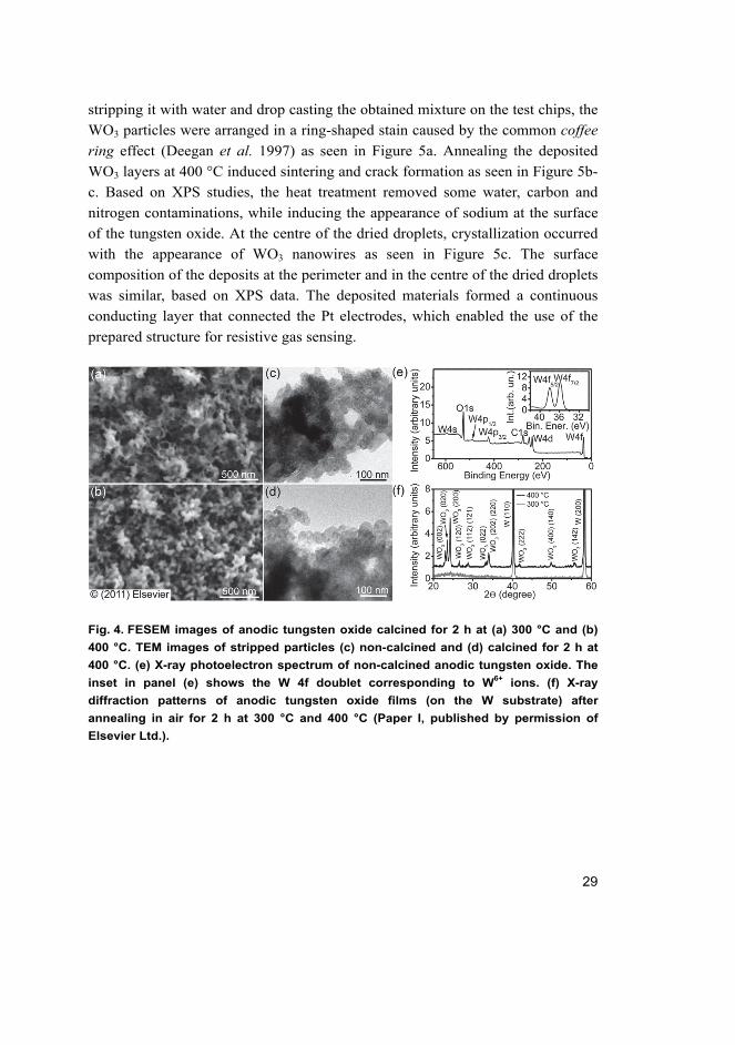
29
stripping it with water and drop casting the obtained mixture on the test chips, the
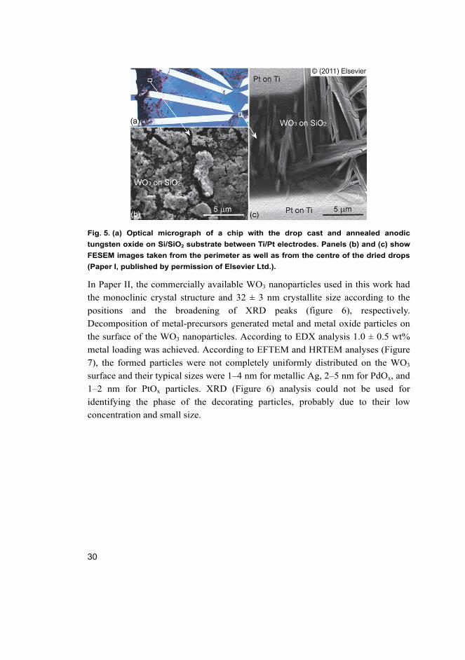
WO3 particles were arranged in a ring-shaped stain caused by the common coffee ring effect (Deegan et al. 1997) as seen in Figure 5a. Annealing the deposited
WO3 layers at 400 °C induced sintering and crack formation as seen in Figure 5b-
c. Based on XPS studies, the heat treatment removed some water, carbon and
nitrogen contaminations, while inducing the appearance of sodium at the surface
of the tungsten oxide. At the centre of the dried droplets, crystallization occurred
with the appearance of WO3 nanowires as seen in Figure 5c. The surface
composition of the deposits at the perimeter and in the centre of the dried droplets
was similar, based on XPS data. The deposited materials formed a continuous
conducting layer that connected the Pt electrodes, which enabled the use of the
prepared structure for resistive gas sensing.
Fig. 4. FESEM images of anodic tungsten oxide calcined for 2 h at (a) 300 °C and (b)
400 °C. TEM images of stripped particles (c) non-calcined and (d) calcined for 2 h at
400 °C. (e) X-ray photoelectron spectrum of non-calcined anodic tungsten oxide. The
inset in panel (e) shows the W 4f doublet corresponding to W6+ ions. (f) X-ray
diffraction patterns of anodic tungsten oxide films (on the W substrate) after
annealing in air for 2 h at 300 °C and 400 °C (Paper I, published by permission of
Elsevier Ltd.).
30
Fig. 5. (a) Optical micrograph of a chip with the drop cast and annealed anodic
tungsten oxide on Si/SiO2 substrate between Ti/Pt electrodes. Panels (b) and (c) show
FESEM images taken from the perimeter as well as from the centre of the dried drops
(Paper I, published by permission of Elsevier Ltd.).
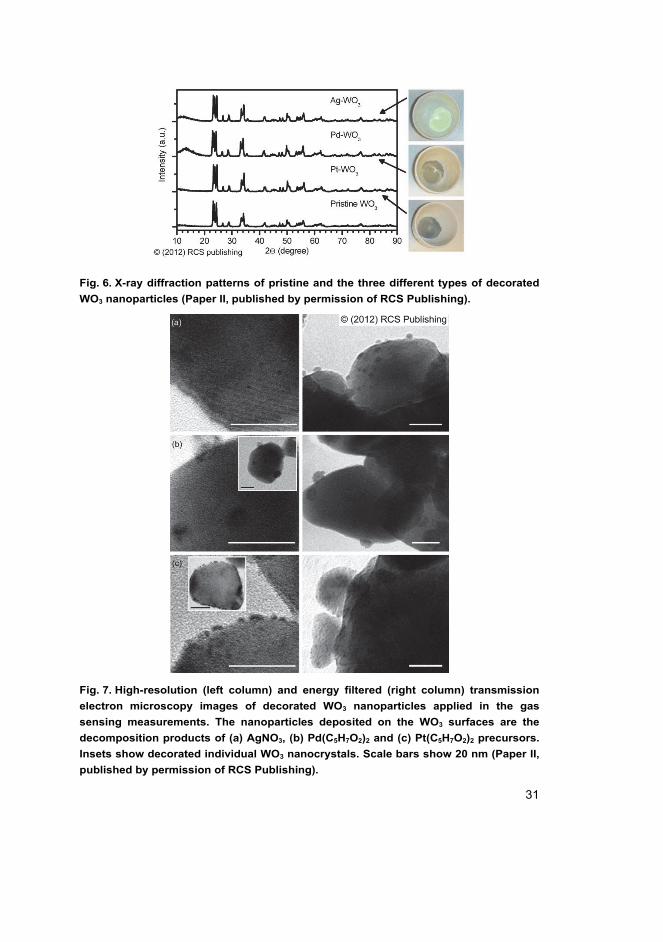
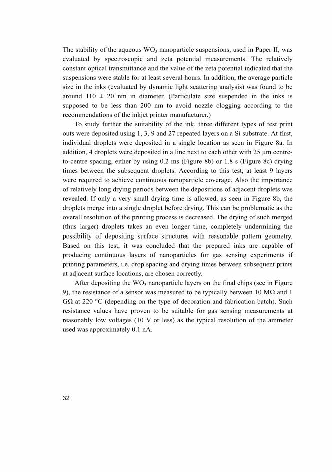
In Paper II, the commercially available WO3 nanoparticles used in this work had
the monoclinic crystal structure and 32 ± 3 nm crystallite size according to the
positions and the broadening of XRD peaks (figure 6), respectively.
Decomposition of metal-precursors generated metal and metal oxide particles on
the surface of the WO3 nanoparticles. According to EDX analysis 1.0 ± 0.5 wt%
metal loading was achieved. According to EFTEM and HRTEM analyses (Figure
7), the formed particles were not completely uniformly distributed on the WO3
surface and their typical sizes were 1–4 nm for metallic Ag, 2–5 nm for PdOx, and
1–2 nm for PtOx particles. XRD (Figure 6) analysis could not be used for
identifying the phase of the decorating particles, probably due to their low
concentration and small size.
31
Fig. 6. X-ray diffraction patterns of pristine and the three different types of decorated
WO3 nanoparticles (Paper II, published by permission of RCS Publishing).
Fig. 7. High-resolution (left column) and energy filtered (right column) transmission
electron microscopy images of decorated WO3 nanoparticles applied in the gas
sensing measurements. The nanoparticles deposited on the WO3 surfaces are the
decomposition products of (a) AgNO3, (b) Pd(C5H7O2)2 and (c) Pt(C5H7O2)2 precursors.
Insets show decorated individual WO3 nanocrystals. Scale bars show 20 nm (Paper II,
published by permission of RCS Publishing).
32
The stability of the aqueous WO3 nanoparticle suspensions, used in Paper II, was
evaluated by spectroscopic and zeta potential measurements. The relatively
constant optical transmittance and the value of the zeta potential indicated that the
suspensions were stable for at least several hours. In addition, the average particle
size in the inks (evaluated by dynamic light scattering analysis) was found to be
around 110 ± 20 nm in diameter. (Particulate size suspended in the inks is
supposed to be less than 200 nm to avoid nozzle clogging according to the
recommendations of the inkjet printer manufacturer.)
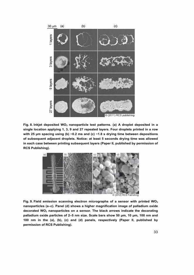
To study further the suitability of the ink, three different types of test print
outs were deposited using 1, 3, 9 and 27 repeated layers on a Si substrate. At first,
individual droplets were deposited in a single location as seen in Figure 8a. In
addition, 4 droplets were deposited in a line next to each other with 25 μm centre-
to-centre spacing, either by using 0.2 ms (Figure 8b) or 1.8 s (Figure 8c) drying
times between the subsequent droplets. According to this test, at least 9 layers
were required to achieve continuous nanoparticle coverage. Also the importance
of relatively long drying periods between the depositions of adjacent droplets was
revealed. If only a very small drying time is allowed, as seen in Figure 8b, the
droplets merge into a single droplet before drying. This can be problematic as the
overall resolution of the printing process is decreased. The drying of such merged
(thus larger) droplets takes an even longer time, completely undermining the
possibility of depositing surface structures with reasonable pattern geometry.
Based on this test, it was concluded that the prepared inks are capable of
producing continuous layers of nanoparticles for gas sensing experiments if
printing parameters, i.e. drop spacing and drying times between subsequent prints
at adjacent surface locations, are chosen correctly.
After depositing the WO3 nanoparticle layers on the final chips (see in Figure
9), the resistance of a sensor was measured to be typically between 10 MΩ and 1
GΩ at 220 °C (depending on the type of decoration and fabrication batch). Such
resistance values have proven to be suitable for gas sensing measurements at
reasonably low voltages (10 V or less) as the typical resolution of the ammeter
used was approximately 0.1 nA.
33
Fig. 8. Inkjet deposited WO3 nanoparticle test patterns. (a) A droplet deposited in a
single location applying 1, 3, 9 and 27 repeated layers. Four droplets printed in a row
with 25 μm spacing using (b) ~0.2 ms and (c) ~1.8 s drying time between depositions
of subsequent adjacent droplets. Notice: at least 5 seconds drying time was allowed
in each case between printing subsequent layers (Paper II, published by permission of
RCS Publishing).
Fig. 9. Field emission scanning electron micrographs of a sensor with printed WO3
nanoparticles (a–c). Panel (d) shows a higher magnification image of palladium oxide
decorated WO3 nanoparticles on a sensor. The black arrows indicate the decorating
palladium oxide particles of 2–5 nm size. Scale bars show 50 μm, 10 μm, 100 nm and
100 nm in the (a), (b), (c) and (d) panels, respectively (Paper II, published by
permission of RCS Publishing).
34
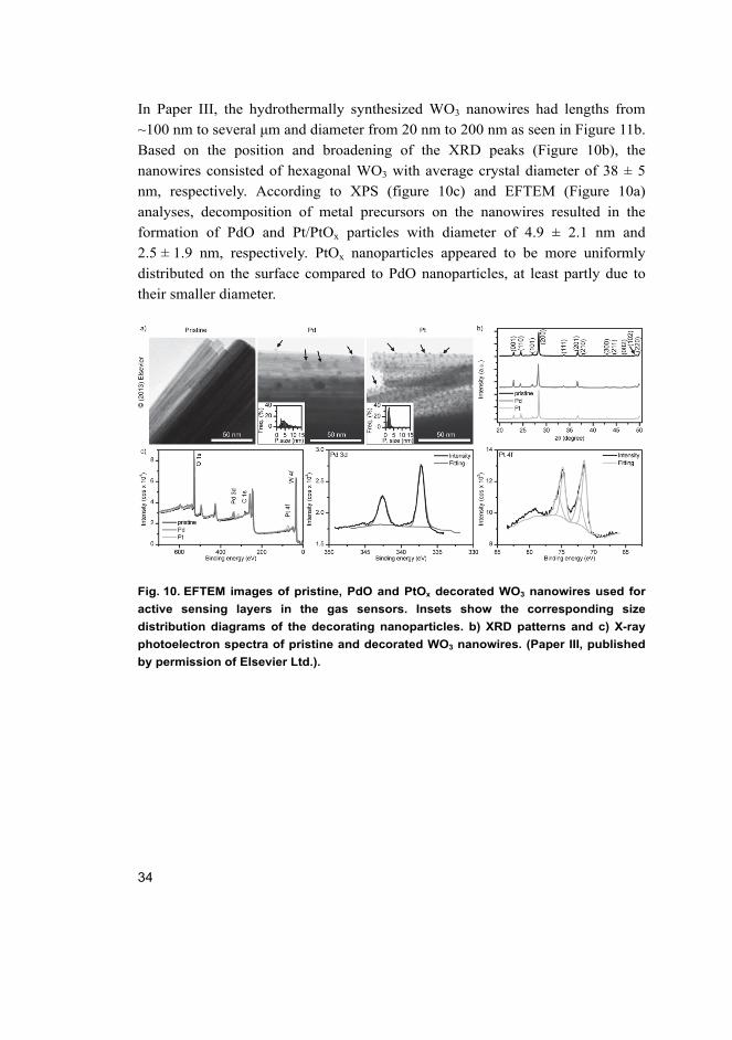
In Paper III, the hydrothermally synthesized WO3 nanowires had lengths from
~100 nm to several μm and diameter from 20 nm to 200 nm as seen in Figure 11b.
Based on the position and broadening of the XRD peaks (Figure 10b), the
nanowires consisted of hexagonal WO3 with average crystal diameter of 38 ± 5
nm, respectively. According to XPS (figure 10c) and EFTEM (Figure 10a)
analyses, decomposition of metal precursors on the nanowires resulted in the
formation of PdO and Pt/PtOx particles with diameter of 4.9 ± 2.1 nm and
2.5 ± 1.9 nm, respectively. PtOx nanoparticles appeared to be more uniformly
distributed on the surface compared to PdO nanoparticles, at least partly due to
their smaller diameter.
Fig. 10. EFTEM images of pristine, PdO and PtOx decorated WO3 nanowires used for
active sensing layers in the gas sensors. Insets show the corresponding size
distribution diagrams of the decorating nanoparticles. b) XRD patterns and c) X-ray
photoelectron spectra of pristine and decorated WO3 nanowires. (Paper III, published
by permission of Elsevier Ltd.).
35
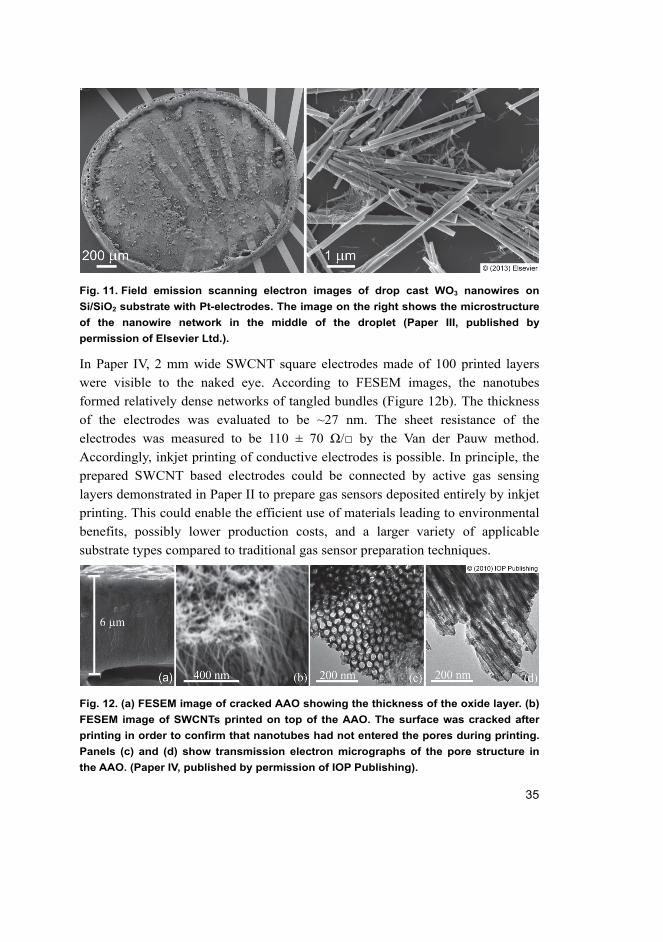
Fig. 11. Field emission scanning electron images of drop cast WO3 nanowires on
Si/SiO2 substrate with Pt-electrodes. The image on the right shows the microstructure
of the nanowire network in the middle of the droplet (Paper III, published by
permission of Elsevier Ltd.).
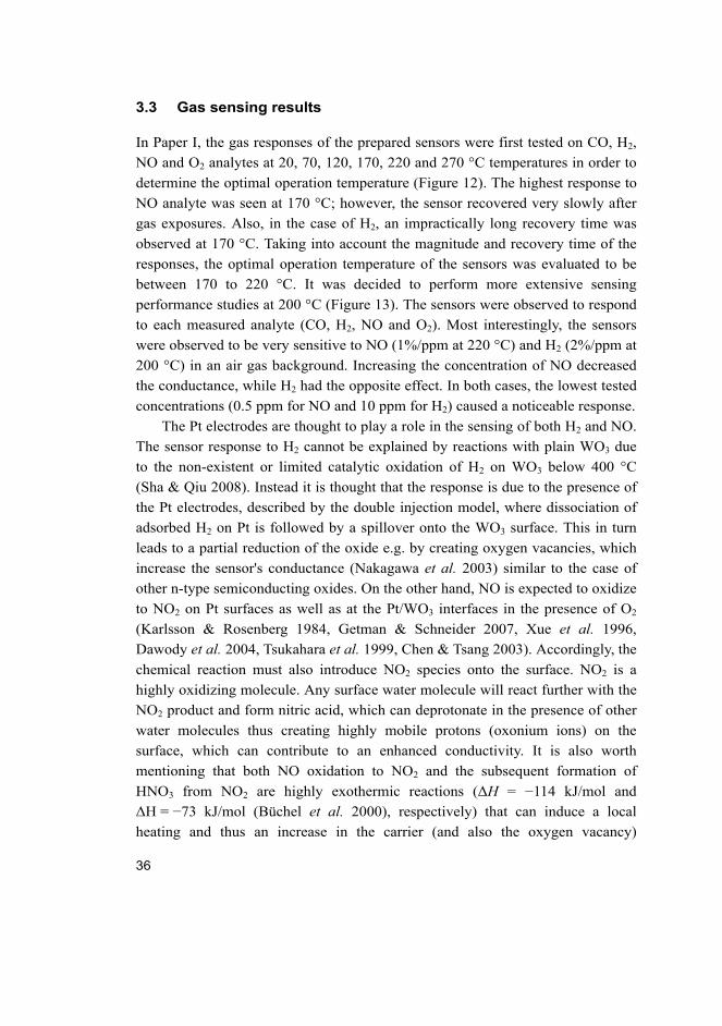
In Paper IV, 2 mm wide SWCNT square electrodes made of 100 printed layers
were visible to the naked eye. According to FESEM images, the nanotubes
formed relatively dense networks of tangled bundles (Figure 12b). The thickness
of the electrodes was evaluated to be ~27 nm. The sheet resistance of the
electrodes was measured to be 110 ± 70 Ω/ by the Van der Pauw method.
Accordingly, inkjet printing of conductive electrodes is possible. In principle, the
prepared SWCNT based electrodes could be connected by active gas sensing
layers demonstrated in Paper II to prepare gas sensors deposited entirely by inkjet
printing. This could enable the efficient use of materials leading to environmental
benefits, possibly lower production costs, and a larger variety of applicable
substrate types compared to traditional gas sensor preparation techniques.
Fig. 12. (a) FESEM image of cracked AAO showing the thickness of the oxide layer. (b)
FESEM image of SWCNTs printed on top of the AAO. The surface was cracked after
printing in order to confirm that nanotubes had not entered the pores during printing.
Panels (c) and (d) show transmission electron micrographs of the pore structure in
the AAO. (Paper IV, published by permission of IOP Publishing).
36
3.3 Gas sensing results
In Paper I, the gas responses of the prepared sensors were first tested on CO, H2,
NO and O2 analytes at 20, 70, 120, 170, 220 and 270 °C temperatures in order to
determine the optimal operation temperature (Figure 12). The highest response to
NO analyte was seen at 170 °C; however, the sensor recovered very slowly after
gas exposures. Also, in the case of H2, an impractically long recovery time was
observed at 170 °C. Taking into account the magnitude and recovery time of the
responses, the optimal operation temperature of the sensors was evaluated to be
between 170 to 220 °C. It was decided to perform more extensive sensing
performance studies at 200 °C (Figure 13). The sensors were observed to respond
to each measured analyte (CO, H2, NO and O2). Most interestingly, the sensors
were observed to be very sensitive to NO (1%/ppm at 220 °C) and H2 (2%/ppm at
200 °C) in an air gas background. Increasing the concentration of NO decreased
the conductance, while H2 had the opposite effect. In both cases, the lowest tested
concentrations (0.5 ppm for NO and 10 ppm for H2) caused a noticeable response.
The Pt electrodes are thought to play a role in the sensing of both H2 and NO.
The sensor response to H2 cannot be explained by reactions with plain WO3 due
to the non-existent or limited catalytic oxidation of H2 on WO3 below 400 °C
(Sha & Qiu 2008). Instead it is thought that the response is due to the presence of
the Pt electrodes, described by the double injection model, where dissociation of
adsorbed H2 on Pt is followed by a spillover onto the WO3 surface. This in turn
leads to a partial reduction of the oxide e.g. by creating oxygen vacancies, which
increase the sensor's conductance (Nakagawa et al. 2003) similar to the case of
other n-type semiconducting oxides. On the other hand, NO is expected to oxidize
to NO2 on Pt surfaces as well as at the Pt/WO3 interfaces in the presence of O2
(Karlsson & Rosenberg 1984, Getman & Schneider 2007, Xue et al. 1996,
Dawody et al. 2004, Tsukahara et al. 1999, Chen & Tsang 2003). Accordingly, the
chemical reaction must also introduce NO2 species onto the surface. NO2 is a
highly oxidizing molecule. Any surface water molecule will react further with the
NO2 product and form nitric acid, which can deprotonate in the presence of other
water molecules thus creating highly mobile protons (oxonium ions) on the
surface, which can contribute to an enhanced conductivity. It is also worth
mentioning that both NO oxidation to NO2 and the subsequent formation of
HNO3 from NO2 are highly exothermic reactions (ΔH = −114 kJ/mol and
ΔH = −73 kJ/mol (Büchel et al. 2000), respectively) that can induce a local
heating and thus an increase in the carrier (and also the oxygen vacancy)
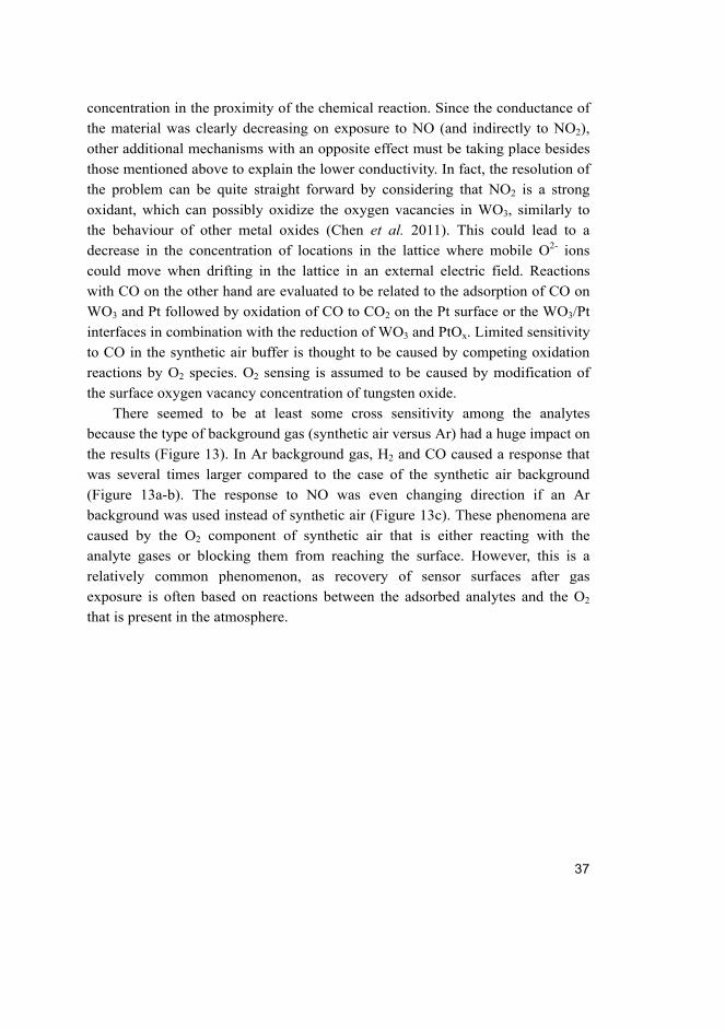
37
concentration in the proximity of the chemical reaction. Since the conductance of
the material was clearly decreasing on exposure to NO (and indirectly to NO2),
other additional mechanisms with an opposite effect must be taking place besides
those mentioned above to explain the lower conductivity. In fact, the resolution of
the problem can be quite straight forward by considering that NO2 is a strong
oxidant, which can possibly oxidize the oxygen vacancies in WO3, similarly to
the behaviour of other metal oxides (Chen et al. 2011). This could lead to a
decrease in the concentration of locations in the lattice where mobile O2- ions
could move when drifting in the lattice in an external electric field. Reactions
with CO on the other hand are evaluated to be related to the adsorption of CO on
WO3 and Pt followed by oxidation of CO to CO2 on the Pt surface or the WO3/Pt
interfaces in combination with the reduction of WO3 and PtOx. Limited sensitivity
to CO in the synthetic air buffer is thought to be caused by competing oxidation
reactions by O2 species. O2 sensing is assumed to be caused by modification of
the surface oxygen vacancy concentration of tungsten oxide.
There seemed to be at least some cross sensitivity among the analytes
because the type of background gas (synthetic air versus Ar) had a huge impact on
the results (Figure 13). In Ar background gas, H2 and CO caused a response that
was several times larger compared to the case of the synthetic air background
(Figure 13a-b). The response to NO was even changing direction if an Ar
background was used instead of synthetic air (Figure 13c). These phenomena are
caused by the O2 component of synthetic air that is either reacting with the
analyte gases or blocking them from reaching the surface. However, this is a
relatively common phenomenon, as recovery of sensor surfaces after gas
exposure is often based on reactions between the adsorbed analytes and the O2
that is present in the atmosphere.
38
Fig. 13. Sensor response to (a) CO in air buffer, (b) H2 in air buffer, (c) NO in air buffer
and (d) O2 in Ar buffer at different temperatures. Measurements at low temperatures
with low currents and heavy noise are not shown (Paper I, published by permission of
Elsevier Ltd.).
39
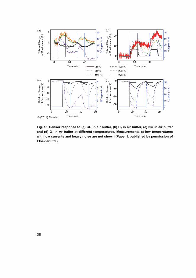
Fig. 14. Sensor response at 200 °C to (a) CO in Ar/air buffers (10, 40, 160, 640 ppm), (b)
H2 in Ar/air buffers (10, 40, 160, 160 ppm), (c) NO in Ar/air buffer (0.5, 2, 8, 32 ppm) and
(d) O2 in Ar buffer (10, 40, 160, 640 ppm) (Paper I, published by permission of Elsevier
Ltd.).
In Paper II, the prepared sensors were found to be most sensitive to H2 and NO
gases, but the signal caused by CO and H2S analytes was also visible (Figure 14).
As expected, the magnitude of the responses depended on the type of the
decorating nanoparticles. In addition, the response and the recovery times had a
similar dependency and were observed to be from 3 minutes to half an hour.
Generally the recovery was slower than the response. The high surface area and
the porous structure of the deposited layers could be responsible for this
behaviour. The signal caused by the most sensitive gases (H2 and NO) was fairly
repeatable during the subsequent measurement cycles as shown in Figures 14a
and 14b. Drift of the sensor signal was mainly noticeable at the beginning of the
measurements, just after reaching the working temperature. The signal was
relatively stable after a few hours of heat treatment at the working temperature of
220 °C.
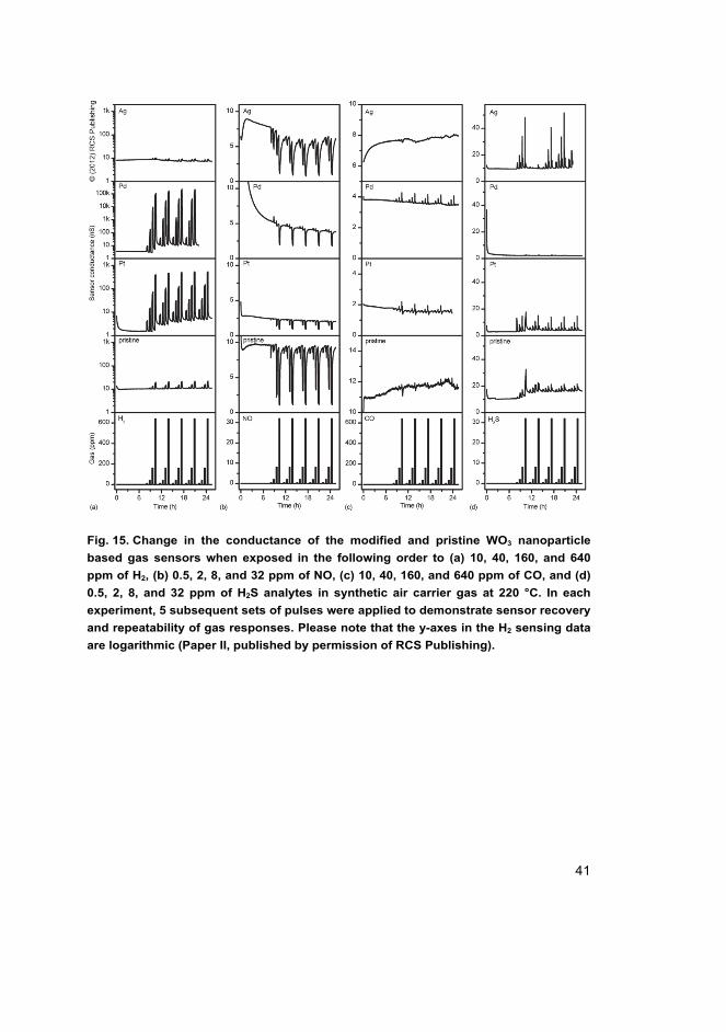
Pristine and Ag-decorated WO3 based gas sensors responded moderately to
H2 (Figure 15b), which could be explained by the catalytic activity of the Pt
electrodes according to the double injection model that was discussed in the case
of Paper I. On the other hand, PdOx and PtOx decorated sensors were observed to
40
be highly sensitive to H2 up to ~10%/ppm and ~1000%/ppm, respectively (Figure
15b). This was probably caused by a similar double injection phenomenon to that
noted in the case of pristine and Ag-decorated WO3 based devices. However, in
the case of PdOx and PtOx nanoparticle decorations, the catalytic effect of the
metals was much higher than that of the Pt electrodes because of dense surface
coverage of small particles on the WO3. Upon exposure to NO, the conductance
of the sensors decreased similarly to the mechanism described in Paper I (figures
14b and 15d); however the presence of decoration particles modified the
responses. The highest response for NO was observed for pristine and Ag-
decorated samples, while it seems that the presence of PdOx or PtOx nanoparticles
inhibited the responses. The limited response in the case of PdOx and PtOx
decorated sensors could be explained by extensive formation of oxidative NO2,
which reduced the effect caused by reducing NO species. The H2S response is
thought to be related to the creation of oxygen vacancies in the tungsten oxide
lattice and the formation of SO2 and H2O at low concentrations and WS2 at higher
concentrations (Okamoto et al. 1980, Steinbrunn & Lattaud 1985). In the case of
metal decorated sensors, the formation of palladium-, platinum- and silver
sulphides is thought to play a role in the response mechanisms (Albers et al. 2001,
Elechguerra et al. 2005). On the other hand, CO oxidation is related to a similar
mechanism as that in the case of Paper I, where oxygen capture from tungsten
oxide leads to the formation of CO2.
41
Fig. 15. Change in the conductance of the modified and pristine WO3 nanoparticle
based gas sensors when exposed in the following order to (a) 10, 40, 160, and 640
ppm of H2, (b) 0.5, 2, 8, and 32 ppm of NO, (c) 10, 40, 160, and 640 ppm of CO, and (d)
0.5, 2, 8, and 32 ppm of H2S analytes in synthetic air carrier gas at 220 °C. In each
experiment, 5 subsequent sets of pulses were applied to demonstrate sensor recovery
and repeatability of gas responses. Please note that the y-axes in the H2 sensing data
are logarithmic (Paper II, published by permission of RCS Publishing).
42
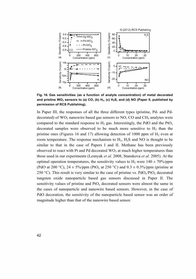
Fig. 16. Gas sensitivities (as a function of analyte concentration) of metal decorated
and pristine WO3 sensors to (a) CO, (b) H2, (c) H2S, and (d) NO (Paper II, published by
permission of RCS Publishing).
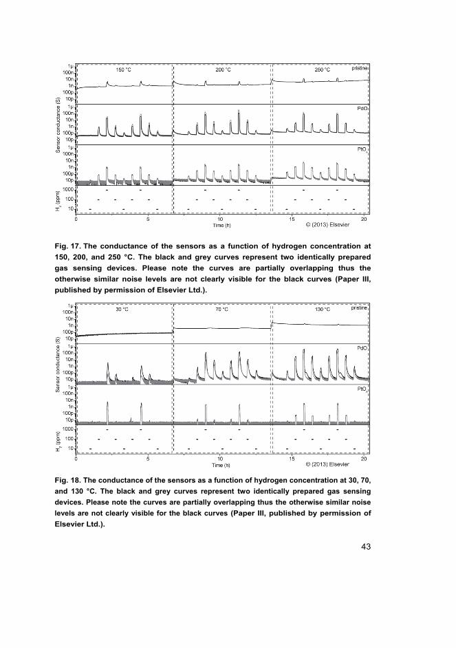
In Paper III, the responses of all the three different types (pristine, Pd- and Pd-
decorated) of WO3 nanowire based gas sensors to NO, CO and CH4 analytes were
compared to the standard response to H2 gas. Interestingly, the PdO and the PtOx
decorated samples were observed to be much more sensitive to H2 than the
pristine ones (Figures 16 and 17) allowing detection of 1000 ppm of H2 even at
room temperature. The response mechanism to H2, H2S and NO is thought to be
similar to that in the case of Papers I and II. Methane has been previously
observed to react with Pt and Pd decorated WO3 at much higher temperatures than
those used in our experiments (Lesnyak et al. 2008, Stanskova et al. 2005). At the
optimal operation temperatures, the sensitivity values to H2 were 140 ± 70%/ppm
(PdO at 200 °C), 24 ± 5%/ppm (PtOx at 250 °C) and 0.3 ± 0.3%/ppm (pristine at
250 °C). This result is very similar to the case of pristine vs. PdOx/PtOx decorated
tungsten oxide nanoparticle based gas sensors discussed in Paper II. The
sensitivity values of pristine and PtOx decorated sensors were almost the same in
the cases of nanoparticle and nanowire based sensors. However, in the case of
PdO decoration, the sensitivity of the nanoparticle based sensor was an order of
magnitude higher than that of the nanowire based sensor.
43
Fig. 17. The conductance of the sensors as a function of hydrogen concentration at
150, 200, and 250 °C. The black and grey curves represent two identically prepared
gas sensing devices. Please note the curves are partially overlapping thus the
otherwise similar noise levels are not clearly visible for the black curves (Paper III,
published by permission of Elsevier Ltd.).
Fig. 18. The conductance of the sensors as a function of hydrogen concentration at 30, 70,
and 130 °C. The black and grey curves represent two identically prepared gas sensing
devices. Please note the curves are partially overlapping thus the otherwise similar noise
levels are not clearly visible for the black curves (Paper III, published by permission of
Elsevier Ltd.).

44
The drift of the sensor signals was more or less visible in all of the discussed
devices. This could be caused by several factors: diffusion of oxygen vacancies in
the bulk of the oxide, semiconductor-metal contact variation at the electrodes,
crack formation and coarsening of the gas sensing particles and other physical
changes, slow desorption of gas molecules from the surface (Di Carlo &
Falasconi 2012, Korotcenkov 2005).
45
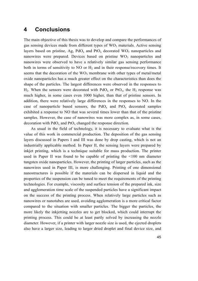
4 Conclusions
The main objective of this thesis was to develop and compare the performances of
gas sensing devices made from different types of WO3 materials. Active sensing
layers based on pristine, Ag, PdOx and PtOx decorated WO3 nanoparticles and
nanowires were prepared. Devices based on pristine WO3 nanoparticles and
nanowires were observed to have a relatively similar gas sensing performance
both in terms of sensitivity to NO or H2 and in their response/recovery times. It
seems that the decoration of the WO3 membrane with other types of metal/metal
oxide nanoparticles has a much greater effect on the characteristics than does the
shape of the particles. The largest differences were observed in the responses to
H2. When the sensors were decorated with PdOx or PtOx, the H2 response was
much higher, in some cases even 1000 higher, than that of pristine sensors. In
addition, there were relatively large differences in the responses to NO. In the
case of nanoparticle based sensors, the PdOx and PtOx decorated samples
exhibited a response to NO that was several times lower than that of the pristine
samples. However, the case of nanowires was more complex as, in some cases,
decoration with PdOx and PtOx changed the response direction.
As usual in the field of technology, it is necessary to evaluate what is the
value of this work in commercial production. The deposition of the gas sensing
layers discussed in Papers I and III was done by drop casting, which is not an
industrially applicable method. In Paper II, the sensing layers were prepared by
inkjet printing, which is a technique suitable for mass production. The printer
used in Paper II was found to be capable of printing the <100 nm diameter
tungsten oxide nanoparticles. However, the printing of larger particles, such as the
nanowires used in Paper III, is more challenging. Printing of one dimensional
nanostructures is possible if the materials can be dispersed in liquid and the
properties of the suspension can be tuned to meet the requirements of the printing
technologies. For example, viscosity and surface tension of the prepared ink, size
and agglomeration time scale of the suspended particles have a significant impact
on the success of the printing process. When relatively large particles such as
nanowires or nanotubes are used, avoiding agglomeration is a more critical factor
compared to the situation with smaller particles. The bigger the particles, the
more likely the inkjetting nozzles are to get blocked, which could interrupt the
printing process. This could be at least partly solved by increasing the nozzle
diameter. However, if a printer with larger nozzle size is used, the ejected droplets
also have a larger size, leading to larger dried droplet and final device size, and
46
possibly less accurate location of the deposited droplets. This could be a problem
because a small gap between the measuring electrodes is preferred to achieve
reasonably high conductance for the gas sensing layers. However, there are
methods to make the nanowires more stable in the inks. Surface functionalization
or surfactants can be used to reduce the attraction between the nanowires. This
technique was demonstrated by the inkjet printing of conductive electrodes based
on COOH-functionalized SWCNTs suspended in aqueous dispersions in Paper IV.
However, it is suggested that mass production of gas sensing devices by inkjet
printing is more straightforward to implement when relatively small particles are
used. In addition, the performance of the nanowire and nanoparticle based gas
sensors prepared for this thesis was relatively similar. When taking into account
these factors, it is believed that nanoparticles are more suitable materials for
inkjet printed gas sensors compared to nanowires.
Even if the proposed inkjet printing method requires relatively long drying
time between depositions of neighbouring droplets on a single sensor, this is not a
problem. If relatively large numbers of sensors are printed at the same time,
printing of a single sensor could take on average only a fraction of a second. The
material cost for one million gas sensing layers produced by the inkjet technique
is estimated to be approximately 1 euro. In practice, the cost to manufacture this
type of gas sensor is entirely dependent on the cost of the measuring electronics.
47
References
Akiyama M, Tamaki J, Miura N & Yamazoe N (1991) Tungsten oxide-based semiconductor sensor highly sensitive to NO and NO2. Chem Lett 20(9): 1611–1614.
Albers P, Pietsch J & Parker SF (2001) Poisoning and deactivation of palladium catalysts. J Mol Catal A Chem 173(1–2): 275–286.
Ando M, Suto S, Suzuki T, Tsuchida T, Nakayama C, Miura N & Yamazoe N (1994) H2S and CH3SH sensor using a thick film of gold-loaded tungsten oxide. Chem Lett 23(2): 335–338.
Aswal DK & Gupta SK (2007) Science and technology of chemiresistor gas sensors. New York NY, Nova Publishers.
Aoki T, Matsushita T, Suzuki A, Tanabe K & Okuda M (2005) Optical recording characteristics of WO3 films grown by pulsed laser deposition method. J Vac Sci Technol A 23(5): 1325–1330.
Balasubramanian K & Burghard M (2005) Chemically functionalized carbon nanotubes. Small 1(2): 180–192.
Barry RG & Chorley RJ (1992) Atmosphere, Wheather and Climate. 6th Revised edition. New York NY, Routledge.
BCC Research LLC (2010) Gas Sensors and Gas Metering: Applications and Markets. Bensebaa F (2013) Nanoparticle technologies: from lab to market. Amsterdam, The
Netherlands, Elsevier. Burstein E (1954) Anomalous optical absorption limit in InSb. Phys Rev 93(3): 632–633. Büchel KH, Moretto HH & Woditsch P (2000) Industrial Inorganic Chemistry. Wiley-VCH,
Weinheim, Germany. Carano M & Flejstad J (2004) Printed Circuit Board Fabrication. In: Harper A (ed) Electronic
Materials and Processes Handbook, Third Edition. New York, McGraw-Hill: 7.3. Carpenter MA, Mathur S, Kolmakov A (2013) Metal Oxide nanomaterials for chemical
Sensors. New York NY, Springer. Carrasco A, Saby C & Bernadet P (1998) Discrimination of Yves Saint Laurent perfumes by an
electric nose. Flavour Frag J 13(5): 335–348. Chang CM, Hon MH & Leu IC (2012) Improvement in CO sensing characteristics by
decorating ZnO nanorod arrays with Pd nanoparticles and the related mechanisms. RCS Adv 2(6): 2469–2475.
Chaudhari GN, Bende AM, Bodade AB, Patil SS & Manorama SV (2006) Detection of liquid petroleum gas using mixed nanosized tungsten oxide-based thick-film semiconductor sensor. Talanta 69(1): 187–191.
Chen L & Tsang SC Ag doped WO3-based powder sensor for the detection of NO gas in air, Sensor Actuator B 89(1–2): 68–75.
Chen M, Wang Z, Han D, Gu F & Guo G (2011) Porous ZnO polygonal nanoflakes: synthesis, use in high-sensitivity NO2 gas sensor, and proposed mechanism of gas sensing. J Phys Chem C 115(26): 12763–12773.
Chiu HC & Tseung ACC (1999) Electrochemical CO2 sensor based on CO2 reduction and subsequent CO oxidation on Pt/WO3 electrode. Electrochem Solid St 2(10): 540–541.
48
Cui S, Pu H, Lu G, Wen Z, Mattson EC, Hirschmugl C, Gajdardziska-Josifovska M, Weinert M & Chen J (2012) Fast and selective room-temperature ammonia sensors using silver nanocrystal-functionalized carbon nanotubes. ACS Appl Mater Interfaces 4(9): 4898–4904.
Cui X, Guo L, Cui F, He Q & Shi J (2009) Electrocatalytic activity and CO tolerance properties of mesostructured Pt/WO3 composite as an anode catalyst for PEMFCs. J Phys Chem C 113(10): 4134–4138.
Dawody J, Skoglundh M & Fridell E (2004) The effect of metal oxide additives (WO3, MoO3, V2O5, Ga2O3) on the oxidation of NO and SO2 over Pt/Al2O3 and Pt/BaO/Al2O3 catalysts. J Mol Catal A: Chem 209(1–2): 215–225.
Dawson DH & Williams DE (1996) Gas-sensitive resistors: surface interaction of chlorine with semiconducting oxides. J Mater Chem 6(3): 409–414.
Deb SK (1969) A novel electrophotographic system. Appl Optics 8(S1): 192–195. Deegan RD, Bakajin O, Dupont TF, Huber G, Nagel SR & Witten TA (1997) Capillary flow as
the cause of ring stains from dried liquid drops. Nature 389: 827–829. Di Carlo S & Falasconi M (2012) Drift correction methods for gas chemical sensors in artificial
olfaction systems: techniques and challenges, In: Wang W (ed) Advances in chemical sensors. InTech , Croatia/China/USA: 305–326.
Dixon RA, Williams JJ, Morris D, Rebane J, Jones FH, Edgell RG & Downes SW (1998) Electronic states at oxygen deficient WO3(001) surfaces: a study by resonant photoemission. Surface Science 399(2–3): 199–211.
Durrani SMA, Khawaja EE, Salim MA, Al-Kuhaili MF & Al-Shukri AM (2002) Effect of preparation conditions on the optical and thermochromic properties of thin films of tungsten oxide. Sol Energ Mat Sol C 71(3): 313–325.
Elechiguerra JL, Larios-Lopez L, Liu C, Garcia-Gutierrez D, Camacho-Bragado A & Yacaman MJ (2005) Corrosion at the nanoscale: the case of silver nanowires and nanoparticles. 17(24): 6042–6052.
Fam DWH Tok AIY, Palaniappan Al, Nopphawan P & Mhaisalkar SG (2009) Selective sensing of hydrogen sulphide using silver nanoparticle decorated carbon nanotubes. Sensor Actuator B 138(1): 189–192.
Freedonia Group, Inc. (2011) Chemical sensors to 2014. Fukuda H, Zohnishi R & Nomura S (2001) Highly sensitive metal-insulator-semiconductor
field-effect transistor sensors for detecting carbon monoxide gas using porous platinum and tungsten oxide thin films. Jpn J Appl Phys 1 40(4B): 2782–2786.
Getman RB & Schneider WF (2007) DFT-based characterization of the multiple adsorption modes of nitrogen oxides on Pt(111). J Phys Chem C 111(1): 389–397.
Global Industry Analysts, Inc. (2010) Chemical sensors – a global market report. Goodenough JB, Hamnett A, Huber G, Hulliger F, Leib M, Ramasesha SK & Werheit H (1984)
Landolt-Bornstein: Numerical Data and Functional Relationships in Science and Technology, New series Group III, Volume 17, Semiconductors Subvolume g, Physics of Non-Tetrahedrally Bonded Binary Compounds III, Springer-Verlag, Heidelberg: 289.
Goodman L (2004) High-tech coal mine canary. J Clin Invest 114(4): 448.
49
Gotoh Y, Inoue K, Ohtake T, Ueda H, Hishida Y & Tsuji H, Ishikawa J (1993) Application of focused ion beam techniques to the fabrication of lateral-type thin-film edge field emitters. Jpn J Appl Phys 33(1): L63–L66.
Greenwood OD, Moulzolf SC, Blau PJ & Lad RJ (1999) The influence of microstructure on tribological properties of WO3 thin films. Wear 232(1): 84–90.
Gu G, Zheng B, Han WQ, Roth S & Liu J (2002) Tungsten oxide nanowires on tungsten substrates. Sens Lett 2(8): 849–851.
Gullapalli SK, Vemuri RS & Ramana CV (2010) Structural transformation induced changes in the optical properties of nanocrystalline tungsten oxide thin films. Appl Phys Lett 96(1): 171903.
Guo YM, Murata N, Ono K & Okazaki T (2005) Production of ultrafine particles of high-temperature tetragonal WO3 by dc arc discharge in Ar-O2 gases. J Nanopart Res 7(1): 101–106.
Hivert B, Hoummady M, Mielle P, Mauvais G, Henrioud JM & Hauden D (1995) A fast and reproducible method for gas sensor screening to flavour compounds. Sensor Actuator B 27(1–3): 242–245.
Hoang-Van C & Zegaoui O (1995) Studies of high surface area Pt/MoO3 and Pt/WO3 catalysts for selective hydrogenation reactions I. Preparation and characterization of catalysts by X-ray diffraction, transmission electron microscopy, hydrogen consumption and carbon monoxide chemisorption. Appl Catal A-Gen 130(1): 89–103.
Ito K, Ohgami T & Nakazawa T (1993) Effect of water on hydrogen-sensitive tungsten oxide films. Sensor Actuator B 12(3): 161–167.
Joshi RK, Hu Q, Alvi F, Joshi N & Kumar A (2009) Au decorated zinc oxide nanowires for CO sensing. J Phys Chem C 113(36): 16199–16202.
Judeinstein P & Livage J (1991) Sol-Gel Synthesis of WO3 thin films. J Mater Chem 1(4): 621–627.
Kanda K & Maekawa T (2005) Development of WO3 thick-film-based sensor for the detection of VOC. Sensor Actuator B 108(1–2): 97–101.
Karlsson HT & Rosenberg HS (1984) Flue gas denitrification. Selective catalytic oxidation of nitric oxide to nitrous oxide. Ind Eng Chem Process Des Dev 23(4): 808–814.
Kenny T (2005) Sensor fundamentals. In Wilson JS (ed) Sensor technology handbook. Burlington MA, Elsevier: 1–20.
Kim KM, Choi KI, Jeong HM, Kim HJ, Kim HR, Lee JH (2012) Highly sensitive and selective trimethylamine sensors using Ru-doped SnO2 hollow spheres. Sensor Actuator B 166–167(1): 733–738.
Koerner WE (1917) The electrolytic behaviour of tungsten. Trans Amer Electrochem Soc 31(1): 221
Kordás K, Tóth G, Levoska J, Huuhtanen M, Keiski R, Härkönen M, George TF & Vähäkangas J (2006) Room temperature chemical deposition of palladium nanoparticles in anodic aluminium oxide templates. Nanotechnology 17(5): 1459.
Korotcenkov G (2005) Gas response control through structural and chemical modification of metal oxide films: state of the art and approaches. Sensor Actuator B 107(1): 209–232.
50
Krebs RE (2006) The history and use of our Earth's chemical elements: a reference guide. 2nd Edition. Westport CT, Greenwood Press.
Krings LHM & Talen W (1998) Wet chemical preparation and characterization of electrochromic WO3. Sol Energ Mat Sol C 54(1–4): 27–37.
Kumar MK & Ramaprabhu S (2006) Nanostructured Pt functionalized multiwalled carbon nanotube based hydrogen sensor. J Phys Chem B 110(23): 11291–11298.
Lakshmi BB, Dorhout PK & Martin CR (1997) Sol-gel template synthesis of semiconductor nanostructures. Chem Mater 9(3): 857–862.
Lamprey H & Ripley (1962) Ultrafine tungsten and molybdenum powders. J Electrochem Soc 109(8): 713–716.
Lassner E & Schubert WD (1999) Tungsten: properties, chemistry, technology of the element, alloys, and chemical compounds. New York NY, Springer.
Lee DH, Chang YJ, Stickle W & Change CH (2007) Functional porous tin oxide thin films fabricated by inkjet printing process. Electrochem Solid St 10(11): K51–K54.
Lesnyak VV, Yatsimirskii VK, Gut IN & Bondyreva OY (2008) Influence of Pt and Pd on the catalytic activity of tungsten and molybdenum oxides in the deep oxidation of methane. Theor Exp Chem 44(2): 134–138.
Li Y, Bando Y & Goldberg D (2003) Quasi-aligned single-crystalline W18O49 nanotubes and nanowires. Adv Mater 15(15): 1294–1296.
Li YJ & Tsai PP (1996) Lacunar pyrochlore-type tungsten oxides as humidity-sensing materials. Solid State Ionics 86–86(2): 1001–1004.
Liao CC, Chen FR & Kai JJ (2006) WO3-x nanowires based electrochromic devices. Sol Energ Mat Sol Cells 90(7–8): 1147–1155.
Lin HM, Hsu CM, Yang HY, Lee PY & Yang CC (1994) Nanocrystalline WO3-based H2S sensors. Sensor Actuator B 22(1): 63–68.
Lou XW & Zeng HC (2003) An inorganic route for controlled synthesis of W18O49 nanorods and nanofibers in solution. Inorg Chem 42(20): 6169–6171.
Luo JY, Deng SZ, Tao YT, Zhao FL, Zhu LF, Gong L, Chen J & Xu NS (2009) Evidence of localized water molecules and their role in the gasochromic effect of WO3 nanowire films. J Phys Chem C 113(36): 15877–15881.
Lyashenko LV & Gorokhovat-skii YB (1975) Photocatalytic oxidation of carbon monoxide on metal oxides. Theor Exp Chem 10(2): 138–142.
Mahadi A. (2007) A new approach to the synthesis of tungsten nanopowders. Master's Thesis. University of Nevada, Reno.
Manorama SV, Izu N, Shin W, Matsubara I & Murayama N (2003) On the platinum sensitization of nanosized cerium dioxide oxygen sensors. Sensor Actuator B 89(3): 299–304.
Mashock M, Yu K, Cui S, Mao S, Lu G & Chen J (2012) Modulating gas sensing properties of CuO nanowires through creation of discrete nanosized p n juntions on their surfaces. ACS Appl Mater Interfaces 4(8): 4192–4199.
Mizsei J & Lantto V (1991) Simultaneous response of work function and resistivity of some SnO2-based samples to H2 and H2S. Sensor Actuator B 4(1–2): 163–168.
51
Mor GK, Shankar K, Paulose M, Varghese OK & Grimes CA (2006) Use of highly-ordered TiO2 arrays in dye-sensitized solar cells. Nano Lett 6(2): 215–218.
Moss TS (1954) The Interpretation of the Properties of Indium Antimonide. Proc Phys Soc 67(10): 775–782.
Mubeen S, Zhang T, Chartuprayoon N, Rheem Y, Mulchandani A, Myung NV & Deshusses MA (2010) Sensitive detection of H2S using gold nanoparticle decorated single-walled carbon nanotubes. Anal Chem 82(1): 250–257.
Mubeen S, Zhang T, Yoo B, Deshusses MA & Myung NV (2007) Palladium nanoparticles decorated single-walled carbon nanotube hydrogen sensor. J Phys Chem C 111(17): 6321–6327.
Mukherjee N, Paulose M, Varghese OK, Mor GK & Grimes CA (2003) Fabrication of nanoporous tungsten oxide by galvanostatic anodization. J Mater Res 18(10): 2296–2299.
Mäklin J, Mustonen T, Kordás K, Saukko S, Tóth G & Vähäkangas J (2007) Nitric oxide gas sensors with functionalized carbon nanotubes. Phys Stat Sol B 244(11): 4298–4302.
Nagy N, Pap AE, Horvath E, Volk J, Barsony I, Deak A & Horvolgyi (2006) Large area self-assembled masking for photonic applications. Appl Phys Lett 89(6): 063104.
Nakagawa H, Yamamoto N, Okazaki S, Chinzei T & Asakura S (2003) A room-temperature operated hydrogen leak sensor. Sensor Actuator B 93(1–3): 468–474.
Niklasson GA & Granqvist CG (2007) Electrochromics for smart windows: thin films of tungsten oxide and nickel oxide, and devices based on these. J Mater Chem 17(2): 127–156.
Niranjan RS, Sainkar SR, Vijayamohanan K & Mulla IS (2002) Ruthenium: tin oxide thin film as a highly selective hydrocarbon sensor. Sensor Actuator B 82(1): 82–88.
Pap A (2005) Investigation of pristine and oxidized porous silicon. Doctoral thesis, University of Oulu.
Patel KJ, Panchal CJ, Kheraj VA & Desai MS (2009) Growth, structural, electrical and optical properties of the thermally evaporated tungsten trioxide (WO3) thin films. Mater Chem Phys 114(1): 475–478.
Patil PS, Patil PR & Ennaoui EA (2000) Characterization of ultrasonic spray pyrolyzed tungsten oxide thin films. Thin Solid Films 370(1–2): 38–44.
Pereira-Ramos JP, Baddour-Hadjean R, Kumagai N & Tanno K (1993) Improvement of the electrochemical behaviour of WO3 as reversible cathodic material for lithium batteries. Electrochim Acta 38(2–3): 431–436.
Polaczek A, Pekala M & Obuszko Z (1994) Magnetic susceptibility and thermoelectric power of tungsten intermediary oxides. J Phys Condens Matter 6(39): 7909.
Pyun SI, Kim D &, Bae JS (1996) Hydrogen transport through r.f.-magnetron sputtered amorphous and crystalline WO3 films. J Alloys Compd 244(1–2): 16–22.
Qi P, Vermesh O, Grecu M, Javey A, Wang Q, Dai H, Peng S & Cho KJ (2003) Toward large arrays of multiplex functionalized carbon nanotube sensors for highly sensitive and selective molecular detection. Nano Lett 3(3): 347–351.
Qu W & Wlodarski (2000) A thin-film sensing element for ozone, humidity and temperature. Sensor Actuator B 64(1–3): 42–48.
52
Quarto FD, Paola AD, Piazza S, Sunseri C (1985) Influence of thermal treatment on the photoelectrochemical behaviour of WO3 photoanodes electrochemically grown. Sol Energ Mater 11(5–6): 419–433.
Regragui M, Addou M, Outzourhit A, Bernéde JC, El Idrissi E., Benseddik E & Kachouane A (2000) Preparation and characterization of pyrolytic spray deposited electrochromic tungsten trioxide films. Thin Solid Films 358(1–2): 40–45.
Regragui M, Jousseaume V, Addou M, Outzourhit A, Bernéde JC & El Idrissi B (2001) Electrical and optical properties of WO3 thin films. Thin Solid Films 397(1–2): 238–243.
Reich S, Leitus G, Popovitz-Biro R, Goldbourt A & Vega S (2009) A possible 2D Hx WO3 superconductor with a Tc of 120 K. J Supercond Nov Magn 22: 343–346.
Rajagopal S, Nataraj D, Mangalaraj D, Djaoued Y, Robichaud J & Khyzhun OY (2009) Controlled growth of WO3 nanostructures with three different morphologies and their structural, optical, and photodecomposition studies. Nanoscale Res Lett 4(11): 1335–1342.
Reiss G & Hütten A (2011) Magnetic nanoparticles. In: Sattler KD (ed) Handbook of nanophysics 3: nanoparticles and quantum dots. Roca Baton FL, CRC Press: 2–1.
Roy S & Basu S (2004) ZnO thin film sensors for detecting dimethyl- and trimethyl-amine vapors. J Mater Sci Mater Electron 15(5): 321–326.
Sawicka KM, Prasad AK, Gouma PI (2005) Metal oxide nanowires for use in chemical sensing applications. Sens Lett 3(1–4): 31–35.
Seiyama T, Kato A, Fujishi K & Nagatani M (1962) A new detector for gaseous components using semiconductive thin films. Anal Chem 34(11): 1502–1503.
Sengupta A, Maji S & Saha H (2010) CBD grown aligned ZnO nanorods based methane sensor and the effect of Pd sensitization. Adv Sci Lett 3(4): 385–392.
Sha L & Qiu ZJ (2008) Thermodynamic calculation on reduction of tungsten oxide in H2 atmosphere. Int J Refract Met Hard Mater 26(4): 363–366.
Sharma RK, Bhatnagar MC, Sharma GL (1998) Mechanism in Nb doped titania oxygen gas sensor. Sensor Actuator B 46(3): 194–201.
Shaver PJ (1967) Activated tungsten oxide gas detectors. Appl Phys Lett 11(8): 255–257. Shedd KB (2012) U.S. geological survey. Mineral Commodity Summaries. URI:
http://minerals.usgs.gov/minerals/pubs/commodity/tungsten/mcs-2012-tungs.pdf. Cited 2013/9/3.
Shen P, Chi N & Chan KY (2000) Morphology of electrodeposited WO3 studied by atomic force microscopy. J Mater Chem 10(3): 697–700.
Simonin L (1869) Underground life; Mines and miners. London, Chapman and Hall. Song XC, Zheng YF, Yang E & Wang Y (2007) Large-scale hydrothermal synthesis of WO3
nanowires in the presence of K2SO4. Mater Lett 61(18): 3904–3908. Stankova M, Vilanova X, Llobet E, Calderer J, Bittencourt C, Pireaux JJ & Correig X (2005)
Influence of the annealing and operating temperatures on the gas-sensing properties of rf sputtered WO3 thin-film sensors. Sensor Actuator B 105(2): 271–277.
Steinbrunn A & Lattaud C (1985) RHEED and Auger study of the MoO3(010) surface interaction with H2S/H2 mixture and pure H2S. Surf Sci 1(1): 279–295.
Szabó M (2011) Diploma thesis, University of Szeged, Hungary.
53
Taguchi N (1962) Japan patent 45–38200. Tamaki J, Zhang Z, Fujimori K, Akiyama M, Harada T, Miura N & Yamazoe N (1994)
Grainsize effects in tungsten oxide-based sensor for nitrogen oxides. J Electrochem Soc 141(8): 2207–2210.
Tsukahara H, Ishida T & Mayumi M (1999) Gas-phase oxidation of nitric oxide: chemical kinetics and rate constant. Nitric Oxide: Biol Chem 3(3): 191–198.
Wilson JS (2005) Sensor Technology Handbook. Burlington MA, Elsevier. Xue E, Seshan K & Ross JRH (1996) Roles of supports, Pt loading and Pt dispersion in the
oxidation of NO to NO2 and of SO2 to SO3. Appl Catal B: Environ 11(1): 65–79. Yoon KH, Shin CW & Kang DH (1997) Photoelectrochemical conversion in a WO3 coated p-
Si photoelectrode: Effect of annealing temperature. J Appl Phys 81(10): 7024–7029. Yu-De W, Zhan-Xian C, Yan-Feng L, Zhen-Lai Z & Xing-Hui W (2001) Electrical and gas-
sensing properties of WO3 semiconductor material. Solid State Electron 45(5): 639–644. Zhao Y, Feng ZC & Liang Y (2000) Pulsed laser deposition of WO3-base film for NO2 gas
sensor application. Sensor Actuator B 66(1–3): 171–173. Zheng H, Ou JZ, Strano MS, Kaner MS, Kaner RB, Mitchell A & Kalantar-zadeh K (2011)
Nanostructured tungsten oxide – properties, synthesis, and applications. Advanced Functional Materials 21(12): 2175–2196.
Zheng H, Tachibana Y & Kalantar-zadeh (2010) Dye-sensitized solar cells based on WO3, Langmuir 26(24): 19148–19152.
Zhu YQ, Hu, Hsu WK, Terrones M, Grobert N, Hare JP, Kroto HW, Walton DRM & Terrones H (1999) Tungsten oxide tree-like structures. Chem Phys Lett 309(5–6): 327–334.

54
55
Original papers
I Kukkola J, Mäklin J, Halonen N, Kyllönen T, Tóth G, Szabó M, Shchukarev A, Mikkola J-P, Jantunen H & Kordás K (2011) Gas sensors based on anodic tungsten oxide. Sensors and Actuators B 153(2): 293–300.
II Kukkola J, Mohl M, Leino A-R, Tóth G, Wu M-C, Shchukarev A, Popov A, Mikkola J-P, Lauri J, Riihimäki M, Lappalainen J, Jantunen H & Kordás K (2012) Inkjet-printed gas sensors: metal decorated WO3 nanoparticles and their gas sensing properties. Journal of Materials Chemistry 22(34): 17878–17886.
III Kukkola J, Mohl M, Leino AR, Mäklin J, Halonen N, Shchukarev A, Konya Z, Jantunen H & Kordás K (2013) Room temperature hydrogen sensors based on metal decorated WO3 nanowires. Sensors and Actuators B 186: 90–95.
IV Kukkola J, Rautio A, Sala G, Pino F, Tóth G, Leino AR, Mäklin J, Jantunen H, Uusimäki A, Kordás K, Gracia E, Terrones M, Shchukarev A & Mikkola JP (2010) Electrical transport through single-wall carbon nanotube-anodic aluminum oxide-aluminum heterostructures. Nanotechnology 21(3): 035707(1–6).
Reprinted with permission from Elsevier Ltd. (I and III), Royal Society of
Chemistry (II) and IOP Publishing (IV).
Original publications are not included in the electronic version of the dissertation.

56
A C T A U N I V E R S I T A T I S O U L U E N S I S
Book orders:Granum: Virtual book storehttp://granum.uta.fi/granum/
S E R I E S C T E C H N I C A
446. Hannu, Jari (2013) Embedded mixed-signal testing on board and system level
447. Sonkki, Marko (2013) Wideband and multi-element antennas for mobileapplications
448. Saarinen, Tuomas (2013) Temporal and spatial variation in the status of acidrivers and potential prevention methods of AS soil-related leaching in peatlandforestry
449. Pirinen, Rauno (2013) Towards regional development by Higher EducationInstitutions : an empirical study of a University of Applied Sciences
450. Mäkinen, Liisa (2013) Improvement of resource efficiency in deinked pulp mill
451. Guo, Yimo (2013) Image and video analysis by local descriptors and deformableimage registration
452. Pantisano, Francesco (2013) Cooperative interference and radio resourcemanagement in self-organizing small cell networks
453. Ojanperä, Tiia (2013) Cross-layer optimized video streaming in heterogeneouswireless networks
454. Pietikäinen, Martti (2013) Metalli- ja elektroniikkateollisuus Oulun eteläisenalueella : kehitys koulutuksen ja teknologian näkökulmasta
455. Pitkäaho, Satu (2013) Catalytic oxidation of chlorinated volatile organiccompounds, dichloromethane and perchloroethylene : new knowledge for theindustrial CVOC emission abatement
456. Morais de Lima, Carlos Héracles (2013) Opportunistic resource and networkmanagement in autonomous packet access systems
457. Nardelli, Pedro Henrique Juliano (2013) Analysis of the spatial throughput ininterference networks
458. Ferreira, Denzil (2013) AWARE: A mobile context instrumentation middlewareto collaboratively understand human behavior
459. Ruusunen, Mika (2013) Signal correlations in biomass combustion – aninformation theoretic analysis
460. Kotelba, Adrian (2013) Theory of rational decision-making and its applications toadaptive transmission
461. Lauri, Janne (2013) Doppler optical coherence tomography in determination ofsuspension viscosity
C462etukansi.fm Page 2 Tuesday, September 3, 2013 12:19 PM
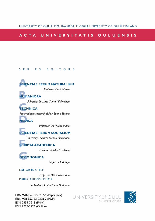
ABCDEFG
UNIVERSITY OF OULU P .O. B 00 F I -90014 UNIVERSITY OF OULU FINLAND
A C T A U N I V E R S I T A T I S O U L U E N S I S
S E R I E S E D I T O R S
SCIENTIAE RERUM NATURALIUM
HUMANIORA
TECHNICA
MEDICA
SCIENTIAE RERUM SOCIALIUM
SCRIPTA ACADEMICA
OECONOMICA
EDITOR IN CHIEF
PUBLICATIONS EDITOR
Professor Esa Hohtola
University Lecturer Santeri Palviainen
Postgraduate research fellow Sanna Taskila
Professor Olli Vuolteenaho
University Lecturer Hannu Heikkinen
Director Sinikka Eskelinen
Professor Jari Juga
Professor Olli Vuolteenaho
Publications Editor Kirsti Nurkkala
ISBN 978-952-62-0207-5 (Paperback)ISBN 978-952-62-0208-2 (PDF)ISSN 0355-3213 (Print)ISSN 1796-2226 (Online)
U N I V E R S I TAT I S O U L U E N S I SACTAC
TECHNICA
U N I V E R S I TAT I S O U L U E N S I SACTAC
TECHNICA
OULU 2013
C 462
Jarmo Kukkola
GAS SENSORS BASED ON NANOSTRUCTURED TUNGSTEN OXIDES
UNIVERSITY OF OULU GRADUATE SCHOOL;UNIVERSITY OF OULU,FACULTY OF TECHNOLOGY,DEPARTMENT OF ELECTRICAL ENGINEERING;INFOTECH OULU
C 462
ACTA
Jarmo K
ukkolaC462etukansi.fm Page 1 Tuesday, September 3, 2013 12:19 PM