Embed Size (px)
Citation preview
2007
Brian Drost
Jon Guerber
Bangda Yang
Mentor: Dr. Pavan Hanumolu
12/6/2007
Oscilloscope On A ChipFinal Design Specification

1. Revision History
Revision Date Description Member.00 10/16/07 Technology Research Reports All.00 10/20/07 Preliminary Minimum Requirements All.05 10/24/07 Preliminary Design Specification Creation Jon.07 10/26/07 Formatting and Introduction Work Jon.10 10/27/07 Introduction
Interface DefinitionRevised Block DiagramCover PageCustomer Requirements
AllBrianBrian and JonJonAll
.25 10/28/07 Competitive AnalysisProduct Space AnalysisFeature Set Definition
AllAllJon
.50 10/29/07 Added Linear Regulators to CA and PSA Jon
.80 10/29/07 Architectural Overview Implementation Approaches Top Level DescriptionEnvironmental Requirements
BangdaBangdaBangdaBangda
.85 10/30/07 Compiled report Jon
.90 10/31/07 Grammatical corrections/formatting All1.00 10/31/07 Added Competitive Analysis
Added Block DiagramPreliminary Design Specification
BrianBrianAll
1.05 11/17/07 Grammatical Revisions (section 2-2.1) Jon1.15 12/01/07 ADC Functional Unit Description
VR Functional Unit DescriptionJonJon
1.25 12/03/07 Block Diagram and Interface Definitions Revisions
Brian
1.50 12/03/07 Microcontroller Unit DescriptionPreliminary Parts ListDAC Unit Description
BrianJonBangda
1.75 12/04/07 User Interface Unit DescriptionTest Plan
BrianAll
1.85 12/05/07 Sampler Level 2 Unit DescriptionMicrocontroller schematics & partsGrader comment revisionsFinal formatting
BangdaBrianJonBrian and Jon
Oscilloscope on a Chip | Group 25
Page 2 of 92
2.00 12/06/07 Final Design Specification All
Oscilloscope on a Chip | Group 25
Page 3 of 92
Contents1. Revision History.............................................................................................................21.1 List of Figures.........................................................................................................5
1.2 List of Tables............................................................................................................62. Introduction............................................................................................................7
2.1 Customer Requirements and Product Background..................................................82.2 Competitive Analysis..............................................................................................10
2.2.1 Product Space Analysis....................................................................................142.3 Feature Set.............................................................................................................18
2.3.1 Minimum Requirements.................................................................................182.3.2 Target Feature Set...........................................................................................19
3. Architectural Overview...........................................................................................203.1 Implementation Approaches..................................................................................22
4. Top Level Description.............................................................................................254.1 Block Diagram........................................................................................................26
4.1.1 Interface Definition.........................................................................................274.1.2 Environment...................................................................................................29
5. Functional Unit Descriptions (Level 1).....................................................................305.1. On-Chip Sampler Functional Block Diagram..........................................................30
5.1.1. Functional Unit Interface Definition...............................................................315.1.2. On-chip Sampler Functional Unit Operation..................................................325.1.3. On-Chip Sampler Simulation Result...............................................................34
5.2. Analog to Digital Converter Functional Unit Description......................................385.2.1 ADC Interface Definition.................................................................................395.2.2 ADC Functional Unit Operation......................................................................40
5.3 Microcontroller Functional Unit Description..........................................................435.3.1. Microcontroller Interface Definition.............................................................455.3.2. Microcontroller Hardware Operation............................................................475.3.3. Microcontroller Schematic Diagram...............................................................505.3.4. Microcontroller Firmware Operation.............................................................51
5.4. Digital to Analog Converter Functional Unit Description......................................555.4.1. Digital to Analog Converter Interface Definition........................................555.4.2. Digital to Analog Unit Operation....................................................................56
5.5. User Interface Functional Unit Description...........................................................585.5.1. User Interface Definitions..............................................................................585.5.2. User Interface Functional Unit Operation......................................................58
5.6. Voltage Regulator Functional Unit Description.....................................................615.6.1 Voltage Regulation Interface Definition.........................................................625.6.2 Voltage Regulation Functional Unit Operation...............................................63
6. Functional Unit Descriptions (Level 2).....................................................................656.1. Multiplexer Block Diagram....................................................................................65
6.1.1. Multiplexer Interface Definition.................................................................656.1.2. Multiplexer Unit Operation............................................................................66
6.2. MOSFET Sampling Circuit Functional Unit Description..........................................67
Oscilloscope on a Chip | Group 25
Page 4 of 92
6.2.1 MOSFET Sampling Circuit Interface Definition................................................676.2.2. MOSFET Sampling Circuit Unit Operation......................................................68
6.3. Output Stage Unit Block Diagram (Level 2)...........................................................716.3.1. Output Stage Interface Definition..................................................................716.3.2 Output Stage Unit Operation..........................................................................716.3.3. Output Stage Unit Simulation........................................................................72
7. Test Plan.................................................................................................................747.1. Functional Test......................................................................................................747.2. System Test...........................................................................................................757.3. Manufacturing Test...............................................................................................777.4. Safety Test.............................................................................................................777.5. Reliability Test.......................................................................................................77
8. Bill of Materials and Suppliers................................................................................788.1. On-chip Sampler Parts List....................................................................................788.2. ADC Parts List.......................................................................................................798.3. Microcontroller Parts List.....................................................................................808.4. DAC Parts List........................................................................................................818.5. User Interface Parts List.......................................................................................81
Appendix A: References.............................................................................................83Appendix B: Naming Conventions and Glossary.........................................................85Appendix C: Media Release.......................................................................................88Appendix D: Revisions Based on Preliminary Design Specification Comments...........89Appendix E: Other Select Revisions from Preliminary Design Specification....................91
Oscilloscope on a Chip | Group 25
Page 5 of 92
1.1 List of FiguresFigure 1: Implementation with on-chip signal generator.................................................22Figure 2: Implementation with digital signal processor...................................................23Figure 3: Top level block diagram....................................................................................25Figure 4: Full system block diagram.................................................................................26Figure 5: On-chip Sampler Top-Level Block Diagram.......................................................30Figure 6: On-chip Sampler Level 1 Block Diagram............................................................30Figure 7: On-chip Sampler External Schematics...............................................................33Figure 8: On-chip Sampler Schematic Part 1....................................................................35Figure 9: On-chip Sampler Schematic Part 2...................................................................36Figure 10: Unfiltered Sampler Output (Before Output Stage)..........................................37Figure 11: Filtered Sampler Output (After Output Stage)................................................37Figure 12: ADC Block Diagram..........................................................................................38Figure 13: ADC Schematics...............................................................................................40Figure 14: Microcontroller Block Diagram.......................................................................44Figure 15: Microcontroller Schematic Diagram................................................................50Figure 16: User Command Code Flow Chart....................................................................51Figure 17: Calibration Code Flow Chart............................................................................52Figure 18: Sampling Code Flow Chart..............................................................................53Figure 19: Error Correction Code Flow Chart...................................................................54Figure 20: Digital-to-Analog Converter Block Diagram....................................................55Figure 21: Digital-to-Analog Converter Schematic...........................................................56Figure 22: User Interface Block Diagram..........................................................................58Figure 23: Preliminary GUI Layout...................................................................................60Figure 24: Voltage Regulator Block Diagram....................................................................61Figure 25: Voltage Regulator Schematics.........................................................................63Figure 26: On-chip Multiplexer Level 2 Block Diagram....................................................65Figure 27: CMOS Implementation of the Inverter and NAND Gate.................................66Figure 28: MOSFET Sampling Circuit Level 2 Block Diagram............................................67Figure 29: Single NMOS Sample-and-Hold Switch...........................................................68Figure 30: CMOS Transmission Gate................................................................................69Figure 31: NMOS Sampling Switch with “Dummy” MOSFET............................................69Figure 32: Buffer Stage Schematic...................................................................................70Figure 33: Output Stage Block Diagram...........................................................................71Figure 34: Output Stage Schematic..................................................................................72Figure 35: Output Stage Simulation Results (Bode Plot)..................................................73
Oscilloscope on a Chip | Group 25
Page 6 of 92

1.2 List of TablesTable 1: Similar Products Competitive Analysis Spreadsheet..........................................10Table 2: Analog to Digital Converters Competitive Analysis Spreadsheet........................11Table 3: Sample and Hold Circuits Competitive Analysis Spreadsheet.............................12Table 4: Linear Voltage Regulator Competitive Analysis Spreadsheet.............................13Table 5: Microcontrollers Competitive Analysis Spreadsheet..........................................13Table 6: Top level interface description...........................................................................25Table 7: Interface Definition Page 1.................................................................................27Table 8: Interface Definition Page 2.................................................................................28Table 9: Typical Environmental Ratings...........................................................................29Table 10: Maximum Environmental Ratings....................................................................29Table 11: Sampler Interface Definition............................................................................31Table 12: ADC Interface Definition...................................................................................39Table 13: Microcontroller Interface Definitions Page 1...................................................45Table 14: Microcontroller Interface Definitions Page 2...................................................46Table 15: Digital to Analog Converter Interface Definition..............................................55Table 16: User Interface Definition..................................................................................58Table 17: Voltage Regulator Interface Definition.............................................................62Table 18: Multiplexer Level 2 Interface Definition...........................................................65Table 19: Multiplexer Output versus Input Select Bit......................................................66Table 20: Multiplexer Output versus Input Select Bit......................................................67Table 21: Output Stage Interface Definition....................................................................71Table 22: Functional Test Plan.........................................................................................74Table 23: System Test Plan Part 1....................................................................................75Table 24: System Test Plan Part.......................................................................................76Table 25: Manufacturing Test Plan..................................................................................77Table 26: Safety Test Plan................................................................................................77Table 27: Reliability Test Plan..........................................................................................77Table 28: Sampler Parts List.............................................................................................78Table 29: ADC Parts List...................................................................................................79Table 30: Microcontroller Parts List.................................................................................80Table 31: Voltage Regulator Parts List.............................................................................82
Oscilloscope on a Chip | Group 25
Page 7 of 92
2. Introduction
This project presents a design to prototype and test an integrated circuit (IC) that allows the user to easily validate the functionality of components inside packaged integrated circuitry and then plot the data on a PC, as if it is an oscilloscope embedded onto the device under test.
Testing of integrated circuits for proper functionality is a mandatory step before shipping them to customers. In order to validate ICs that are inside a package, the signals under test are brought off-chip through bond pads. Automatic test equipment (ATE) interfaces with the IC through these pads and performs very rudimentary tests. For example, while testing a single transistor, the tester generates a plot describing the voltage and the current characteristics of the transistor.
As the size of ICs decrease and the complexity and bandwidth of the devices increase, the testing of sensitive nodes becomes increasingly difficult. Often this is due to the loading and other parasitic effects associated with the tester. Three major limitations were associated with the conventional approach of probing ICs using an external device:
(a) The parasitics associated with the bulky probes of the tester and the difficulty in accessing critical nets in a large IC caused inaccuracies(b) The extensive test-time incurs severe cost penalty on the IC manufacturer(c) The high cost of the ATE as well as the bond pads required for probing the signals
This project overcomes these limitations by designing test circuitry that can preserve the waveform characteristic of the node under test at a much lower frequency than the actual speed of the node. The parasitic effects and the loading will be further reduced with the absence of the probes on the output. Also, the output will only consist of digital interface so the data is again more immune to analog noises, and can be easily transferred to and processed by a computer. The user can then test any transistor inside the packaged IC by plotting its characteristics on a PC without the high cost of an ATE.
This oscilloscope on a chip will consist of three major sub-systems: the on-chip sampler, the analog-to-digital converter (ADC), and the embedded microcontroller system. The on-chip sampler detects the node voltage under test at a desired frequency slightly lower than the interested node frequency. The difference of the two frequencies is then fed into an ADC, which converts the analog signal into a stream of digital data. The digital data, using either parallel or serial means, will be processed with a microcontroller before they are compatible with PC.
Oscilloscope on a Chip | Group 25
Page 8 of 92
2.1 Customer Requirements and Product Background
The recent interest in non-intrusive testing of ICs arises from the parasitic analog behavior of digital signals at high speed. The traditional digital test technologies such asAutomatic Test Generation Pattern (ATGP) and Built-in Self-Test (BIST) lack the dedicated features that address the analog issues such as crosstalk, interference, and phase noise of traces and other high-speed interconnects [1]. Furthermore, the two common alternatives for testing analog signals are electron beam probing and pico-probing, both of which are expensive, difficult, and most importantly, disrupt the signal under test [2]. For example, a conventional low impedance oscilloscope probe, even with capacitances of pFs (picofarads - about a thousand to a million times less than most discrete capacitors), is usually enough to significantly disrupt the voltages and currents on an IC. Also, the advancement in system-on-a-chip design drives the need to test analog signal blocks embedded in mainly digital Very Large System Integration (VLSI), where accessing analog signals is highly limited [1]. The “oscilloscope-on-a-chip” design will attempt to minimize the issues with each of the traditional testing methods mentioned above by providing an on-chip sampler in the same device to capture the waveform in the time domain.
There is already precedent for moving test circuitry onto a chip. Boundary scan is a technology for digital circuits that allows a tester to drive signals into and read signals out of a chip through the pins of a chip. Many people know this technology as JTAG.However, boundary scan can only be used for digital circuits and is limited since only the inputs and outputs to the chip can be controlled and read. If the analog properties of a circuit need to be tested, the circuit must still be probed. An on-chip oscilloscope could be a cheaper method of testing and debugging analog chips or for examining the analog properties of digital ICs.
The targeted customers of the on-chip oscilloscope design span across the semiconductor industry due to the mandatory nature of chip testing. Customers range from giant multinational chip design and manufacture corporations such as Intel, and major semiconductor foundries like Taiwan Manufacturing Semiconductor Company (TMSC), to small chip design center without fabrication facilities. Even though usually as competitors, most ATEs such as Agilent Technologies or Teradyne would likely to pursue the technology for the advantages of the non-intrusive testing of the analog waveforms. The automated testers most ATE companies used to generate test patterns and check outputs are only reliable for digital logic values due to the complexities of the multiple scan chain setups [2]. Even state of the art probing equipment such as the Zyvex KZ100, can only examine as far as the DC characteristics of a transistor or simple circuit [3]. Thus fabrication facilities would utilize this technology for validation, possibly in tandem with an ATE.
Oscilloscope on a Chip | Group 25
Page 9 of 92

The primary feature customers would find appealing is the quantified measurement accuracy and performance over traditional testing methods. Because of the timing accuracy and resolution of the sampler, the end user would likely notice little difference between data transmitted from the on-chip oscilloscope and the standard test-bench version. Another major feature of this product is the minimal required implementation space and complexity. The product would be unappealing if it forces a chip designer to increase the size or complexity of their IC in order to include this circuitry. The market for this product is not only vast, but is continuing to grow. While the on-chip oscilloscope design is not generally thought of as a product, it can be viewed as valuable intellectual property and marketed as such.
In a way the on-chip oscilloscope is a stand-alone system because the chip designer can use it as a block that can be easily fit into other CMOS circuitry. But even though the on-chip oscilloscope offers better performance for sensing analog signals, it would always be integrated into a larger VLSI system. One of the trade-offs the customer would consider when using this product is between its performance and its compatibility over a variety of systems. When testing analog nodes in two very different types of VLSI systems, how well the oscilloscope functions across the different processes parameters such as width and length sizes and the thickness of the materials would have to come into question.
Other considerations for integrated the on-chip oscilloscope is its added power consumption and manufacturing cost. In the age of growing environmental wariness is essential to count the cost of each added watt to a circuit design. Added to this would be the cost of losing silicon space to a feature that has no real bearing in the end-user functionality. The customer would then need to decide if the on-chip oscilloscope should be used in a prototype environment or in mass production
Oscilloscope on a Chip | Group 25
Page 10 of 92
2.2 Competitive Analysis
Table 1: Similar Products Competitive Analysis Spreadsheet
Sampling Head on a ChipOscilloscope on a Chip | Group 25
Page 11 of 92
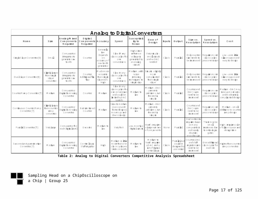
Table 2: Analog to Digital Converters Competitive Analysis Spreadsheet
Sampling Head on a ChipOscilloscope on a Chip | Group 25
Page 12 of 92

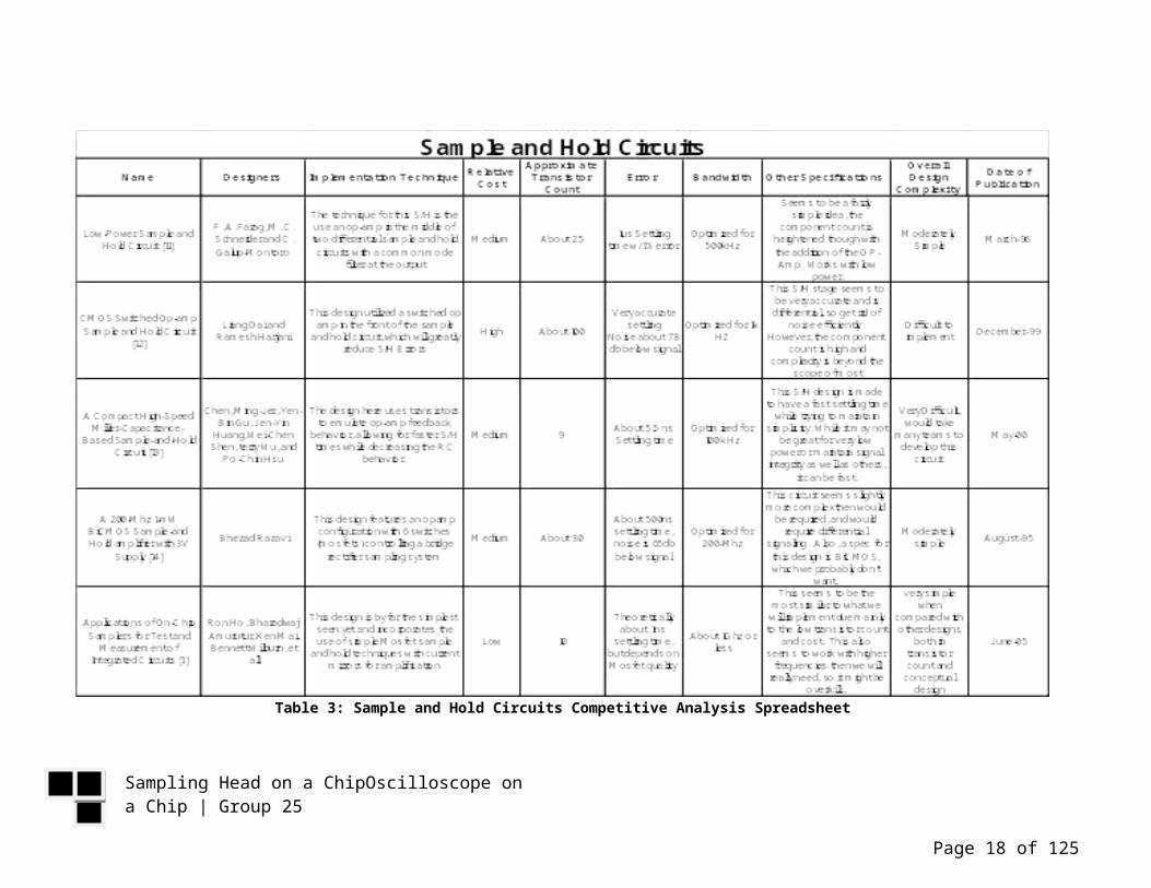
Table 3: Sample and Hold Circuits Competitive Analysis Spreadsheet
Sampling Head on a ChipOscilloscope on a Chip | Group 25
Page 13 of 92
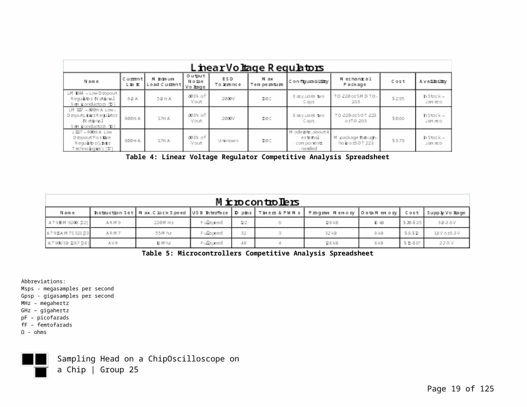
Table 4: Linear Voltage Regulator Competitive Analysis Spreadsheet
Table 5: Microcontrollers Competitive Analysis Spreadsheet
Abbreviations:Msps - megasamples per secondGpsp - gigasamples per secondMHz – megahertzGHz – gigahertzpF – picofaradsfF – femtofaradsΩ - ohms
Sampling Head on a ChipOscilloscope on a Chip | Group 25
Page 14 of 92
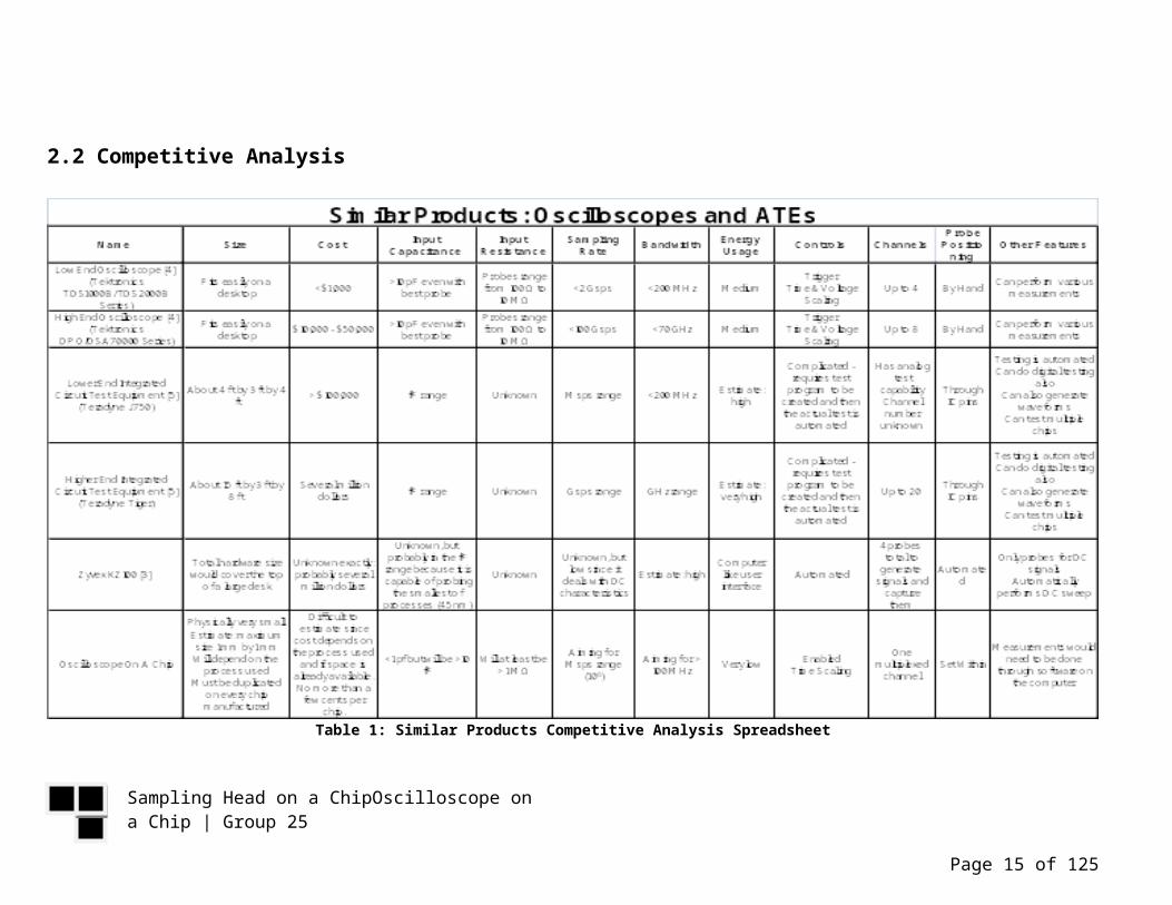
2.2.1 Product Space Analysis
Direct Competitor 1: Oscilloscopes The closest comparable product in terms of function to our sampler on a chip design is the standard oscilloscope. There are a wide varieties of oscilloscopes using different types of probes, and their sampling rates move from the megasamples per second (106 samples per second) range up to even near one hundred gigasamples per second (1011
samples per second) [4]. The current goal for this product is 1 megasample per second, so we will not be competing with high speed oscilloscopes.
As previously stated, the advantage of building an oscilloscope onto an IC comes from being less intrusive when the signal is measured. The best oscilloscope probes have capacitances greater than 10 pF (10-11 farads) where the oscilloscope on a chip would be able to move into fF (10-15 farads) range. Of course, it would be very difficult to position an oscilloscope probe correctly to probe the tiny traces on an IC, but even if it were possible, the best oscilloscope with the best probe would interfere with the signals they were probing. So even though the market is mature with many companies specializing in the design and production of oscilloscopes, our product should not be competing directly against them.
Direct Competitor 2: ATEsInstead the closest competition will be the ATE systems for testing ICs. Testing chips requires expensive equipment that can precisely position the probes and has input capacitances in the fF range. The cheapest test systems are $100,000, but can cost millions of dollars [5]. Of course, these test fixtures also perform many other tests than just analog testing, and they also include a signal generator to produce the signals. However, they can only apply signals to and probe signals out of a chip external pins [5]. Internal traces cannot be tested directly. In this respect, the oscilloscope on a chip has an advantage because it can sample internal signals. Devices do exist that can look into the chip. The Zyvex KZ100 can examine the DC characteristics of individual transistors [3], but our team was unable to find an example of a device that can provide the same function as the oscilloscope on a chip.
While the cost of test equipment may be minimal to a large manufacturer of ICs, it is prohibitive for smaller manufacturers or small chip designers who need to test or debug their circuits. Another major factor all the ATE systems failed to address is software reliability. Even the overall system reliability over time has been rarely found in datasheet. Specifications on parameters such as Mean Time Between Failures (MTBF) and Mean Time To Repair (MTTR) are not mentioned on the product descriptions.This is why a space exists for the oscilloscope on a chip. Our circuit will not be a replacement for test equipment for large manufacturers, but it can find a niche as a cheaper and more reliable alternative to expensive IC probing systems.
Sampling Head on a ChipOscilloscope on a Chip | Group 25
Page 15 of 92
Analog to Digital ConvertersThe second portion of the competitive analysis spreadsheet focuses on analog to digital converters (ADC). The simplest varieties of ADCs are the single slope and dual slope converters [6], [7]. While they cannot convert at high speeds, they are simple to build. Dual slope converters can be highly accurate if designed correctly [7]. Since we are inexperienced ADC designers, we will probably look closely at these designs since they are the simplest to implement, even if they are not the fastest methods.
The counter ramp converter and the continuous counter ramp converter are very similar in construction. They are fairly small designs too, but need a DAC (digital to analog converter) to function [7]. Designing a high resolution and high speed DAC is a challenge, so this will make it difficult to use this design. The successive approximation converter has the same drawback, and requires additional circuitry to control its operation [7]. These systems increase accuracy and speed at the expense of complexity, which may not be a beneficial trade off given our inexperience with IC design.
The parallel converter (also called a flash converter) is very fast and does not require a DAC [6], [7]. However it does need a lot of silicon space and its space needs approximately double for every additional bit of resolution added [7]. Unless we want only a few bits of resolution, the parallel converter will be too large with too many components for us to design. At any reasonable resolution, it will easily exceed the size and component requirements we want to meet, so it is not a very viable option.
While all the ADCs have advantages and drawbacks, our primary requirement for an ADC is something that provide decent resolution (6-10 bits, which is 64 to 1024 possible output levels) and accuracy that we can succeed in designing. For this reason, the two slope converters look the most appealing.
The Digital InterfaceAlso included in the competitive analysis is some information on digital interfaces. The easiest interface to implement for getting data out of the chip will be a parallel bus where each line is used to transmit is a bit from the ADC. However at high speeds parallel buses can have trouble with the bits of data not arriving at the same time. This is a concern we will have to pay attention to if we go the parallel route.
A serial bus could also be used. It will reduce the number of pins used, does not require a lot of additional hardware, and does not have the problem with bits arriving at different times. It would require that the data be transferred at even faster speeds. If our clock speed gets high enough, high speed effects will appear that will make implementing this bus more difficult.
Several simple serial bus protocols already exist such as SPI (serial peripheral interface) and UART (universal asynchronous receive transmit), but these are not designed to run
Sampling Head on a ChipOscilloscope on a Chip | Group 25
Page 16 of 92
at speeds of more than about 3 MHz (megahertz - 106 cycles per second) [8]. USB (universal serial bus) high speed can run at speeds as high as around 500 MHz.
The JTAG protocol used for boundary scan is also a possibility. Both JTAG and SPI would require a simple interface (not much more than one or two shift registers). JTAG has the advantage that it can be run at speeds as high as 100 MHz. However, UART or USB are asynchronous (not matched to a clock) and their interfaces would be much more complicated to implement.
In terms of chip design, the parallel bus or the simple serial bus solution would make our life easier, but they cannot interface directly to a computer. JTAG and SPI would also be fairly simple options, but would also require a conversion to a different bus to talk with a computer. The best option is to use a bus that has a simple interface on the chip side and then use a component like a microcontroller or FPGA to convert to a bus that can be connected to a computer.
Sampler Silicon CellOne of the integral parts of the silicon chip itself is the sampler module. This is the block within the chip that is responsible for reading the voltage of the signal under test and then sending this data to some sort of a latch. Perhaps the most vital goal of our sampler circuitry is to keep the design simple and the transistor count low. Thus of the researched sample and hold circuits, an idea like that proposed by R. Ho et al. utilizing only a few sampling MOSFETs would be ideal [1].
While this is a fairly new field of research some other ideas have been considered for sample and hold circuitry built upon the basic concepts of the simple MOSFET configuration. They were often able to extend their range to higher bandwidths and minimize distortion thought the use of op-amps, switched components, and intrinsic capacitances [11], [12], [13]. A key feature missing from these configurations however is simplicity and portability.
Linear RegulatorIn order to successfully implement microcontroller and other added functionality, it is important to utilize a voltage regulator to change the 5V coming in from the computer interface into a more usable 3.3V. While the design of regulators tends to be rather simple it was important to investigate different components in case they would be problems with one of our selections.
The research of these regulators shows that issues like regulator noise and max currents should not be an issue. A variety of linear regulators are available off the shelf. The focus for the silicon on a chip design team was cost of the regulator, as the performance of all of them tended to be exemplary. For this project, there should not be a need for any regulator to exceed $2 in cost.
Sampling Head on a ChipOscilloscope on a Chip | Group 25
Page 17 of 92
MicrocontrollerThe microcontroller is the link between the user’s interface on the computer and the on-chip sampler. It has three main functions in the design:
1.) To provide control signals to the on-chip sampler and ADC
2.) To convert data from the ADC’s output to USB in order to interface with a personal computer
3.) To provide clocks for the ADC and sampler
These three requirements will determine which microcontroller will be used. The built-in USB interface is mandatory as long the computer/microcontroller interface will be USB. Slower microcontrollers will be cheaper, but it will be difficult to produce high frequency clocks and transfer data at a fast enough rate. Faster microcontrollers will be more expensive and more complicated to program. Also larger microcontrollers could cause manufacturing problems when the board is built.
Considering these tradeoffs and requirements, the simpler AVR microcontroller will be easy to program, but lacks a high clock frequency and may have trouble reading data from the ADC at rates near 1 MHz. The ARM7 microcontroller has a faster clock rate, a lower price, and is capable of producing clock frequencies up to 200 MHz. However, this clock is limited in the frequencies it can produce. The ARM9 is expensive and contains many more pins than we need, but can produce the clocks we need and will have no problem reading data from the ADC at fast rates. Overall, the ARM9 meets the requirements, but a cheaper solution may be using the ARM7 or AVR microcontroller with additional hardware.
Sampling Head on a ChipOscilloscope on a Chip | Group 25
Page 18 of 92
2.3 Feature Set
2.3.1 Minimum Requirements
1. Non-intrusive probing of signals; original signal magnitude deviates by no more
than 10%
2. Converts analog signals to digital data transferable to standard PC
3. Includes a calibration mode for the creation of a transfer function lookup table
4. On-chip sampler consumes less than 5mm2 of silicon real estate
5. Circuit consumes no more than 1W of power
6. Input frequency bandwidth at 1MHz
7. Sampling and input period difference, ∆f, at 10% of input period, fIN
8. Reconstruct a signal with frequency fIN ± 50%
9. Overall sampling period jitter less than 10% of ∆T
10. 6-bit digital resolution, or 64 digital quantization levels
11. All needed design collaterals for validation and portability, which including but
not limited to:
a. PCB board layout and schematic
b. Silicon layout and chip schematic
c. MATLAB and SPICE simulation
d. User interface software source code
Sampling Head on a ChipOscilloscope on a Chip | Group 25
Page 19 of 92
2.3.2 Target Feature Set
Non-Intrusive solution for probing on-chip signals
Outputs are easily defined on a PC-based user interface
Signals with bandwidths up to 1 MHz can be detected with ease
Precise determination of sampled voltage level with at least 6-bit resolution
Design collateral allows for simple replication within a custom chip environment
Simple and low power operation: 5V off USB, Wall Power, or Power Supply Input
Low cost alternative to Automatic Test Equipments
Sampling Head on a ChipOscilloscope on a Chip | Group 25
Page 20 of 92
3. Architectural OverviewAs stated in the introduction, the on-chip oscilloscope is a built-in self-test (BIST) circuit that is integrated into a larger system, such as very large system integration (VLSI) or mixed signal IC designs, which would be the system under test (SUT). Its goal is to probe fast, sensitive analog nodes non-intrusively. Non-intrusive testing is defined as testing that minimizes change to the timing or the processing characteristics of the system under test [18]. For the current on-chip oscilloscope design, the non-intrusive test system consists of an on-chip MOS sampler, an analog-to-digital convertor (ADC), and a microcontroller to first collect timing and raw data. It then transfers that information to be processed on another platform, in this case a PC.
In theory the on-chip oscilloscope accomplishes its goal of non-intrusive testing in two ways: the frequency down conversion of high-speed signals by 10 to 100 orders of magnitude with MOS transistor sub-sampling, and the reduction of capacitive and inductive parasitics associated with the test probes. From the product space analysis, the best oscilloscope probes have capacitances greater than 10 pF however, the on-chip sampler would be able to move into fF range. The on-chip MOS transistor sampler relies on well-known sub-sampling techniques and requires two synchronous clocks [19]. One of the two acts as the input signal and the other one clocks the on-chip sampler. Only the difference between the two clocks, or the beat frequency, will be the output from the on-chip sampler [19]. Both of these two clock sources, as well as the clock for the ADC, will be provided by the microcontroller. A calibration mode is implemented by injecting a known direct current (DC) bias to the sampler and checking the sampler output accordingly.
The sampled analog voltage from the MOS samplers is buffered through two current mirrors with approximately 100 times amplification, and is then transferred off the chip to a minimum 6-bit, 100MHz ADC with a signal-to-noise (SNR) ratio of at least 40dB. The 100MHz is fast enough for sampling the slow output from the sampler, which would be the beat frequency between the sampling clock and the input signal in the low kHz range. This SNR value is estimated from the quantization noise to SNR equation, SNR = 6.02n + 1.76dB [20], where ‘n’ is the number of bits, for which 6 bits results in a minimum SNR of 37.9dB. The preferred option will be to have the ADC on the chip, since it reduces the interconnections and loading effect thus simplifying future automation and test integration for the customer. However, the current prototype design calls for the ADC to be discrete, which may increase the noise and inaccuracies, but eliminates the risks and the additional resources of adding another system on the silicon real estate, which is a critical feature of the on-chip oscilloscope.
All the control signals and the clock sources are provided by the microcontroller, which is also the main interface to the PC. The control signals it provides include the input select multiplexer (MUX) that chooses either the calibration bias or the actual input
Sampling Head on a ChipOscilloscope on a Chip | Group 25
Page 21 of 92

signal for the on-chip sampler, and the sampler enable that can be used to drive the sampling MOS into cutoff when desired. Most importantly, the microcontroller provides the translation of signal between the sampling system and the PC, which provides and interface for the end user. The microcontroller should convert the ADC output into a protocol that is serial, synchronous and full-duplex. The interface planned on implementing is the universal serial bus (USB). In short, using an external device like a microcontroller provides the end user an easy control interface to the oscilloscope on a chip’s operation with additional features.
The maximum input bandwidth is one the most important performance parameters of the on-chip oscilloscope, and minimum requirement designates the input bandwidth to be at least 1MHz, meaning that any input signal with a frequency over 1MHz will have a possible 3dB or more reduction in amplitude. This parameter is mainly determined by the on-chip sampler’s resistance-capacitor (RC) time constant of the on-chip MOS sample-and-hold circuit, as well as the 3dB cutoff frequency based on the MOS parasitics. The MOS on-resistance can be characterized by the process parameter such as the width and the length of the silicon substrate, as well as the gate-source bias voltage and the threshold potential. The current plan proposes to have the silicon fabricated with Metal Oxide Semiconductor Implementation Service (MOSIS)’s 0.35 micron technology. It is expected that the on-chip sampler can be synthesized into an area of approximately 1mm2. In summary, the major factors causing performance limitations for the on-chip oscilloscope include:
1.) The capacitive load of the MOS transistors [20]
2.) The low bandwidth of analog buffers
3.) The noise of the clock source for the on-chip sampler and the ADC
4.) The noise of the power supply
The accuracy of the output waveform with this sub-sampling technique replies on the difference between the sampling period and the input period, or Tsample – Tinput = ΔT. Based on MATLAB simulations, a maximum ΔT of 0.1 (10%) still results in acceptable output waveforms based on visual inspection. The jitter noise of the clocking system is required to be less than 10% of ΔT. Along with the other requirements, this definition translates into a value of 1 / (1MHz * 10% * 10%) = 10ns. At higher frequencies, the phase noise in the clock source also limits the resolution and the SNR of the ADC [20]. The analog buffers are used to compensate for the low driving capability of the MOS transistors.
Sampling Head on a ChipOscilloscope on a Chip | Group 25
Page 22 of 92
3.1 Implementation Approaches
The most basic measurement approach for analog testing with an oscilloscope requires a signal generator that is used to excite the SUT with a known signal, and a sensing circuitry to detect the output of the SUT [21]. The “oscilloscope on a chip” design focuses mainly with the sensing portion of the test. As mentioned in the previous section, the current implementation consists of an on-chip sampler, an ADC and a microcontroller, each component, as well as the entire system, had different approaches.
In order for the on-chip sampler to have the required sub-sampling with minimum parasitic, it is imperative that it be placed on the same silicon die as the desired SUT. Being on-chip, the sampling system also reduces interconnects and the device loading effect. However, the number of approaches for designing the sampling circuitry is limited due to the high cost of implementing passive components such as resistors inside the monolithic substrate. The sampler also requires a stable clock source. The question then comes to the implantation of this device. Since the minimum target feature set requires the output data transferable to a PC, the use ADC is also evitable. Implementing an on-chip ADC is also considered, as well as the different methods for transferring the digital off-chip to the PC.
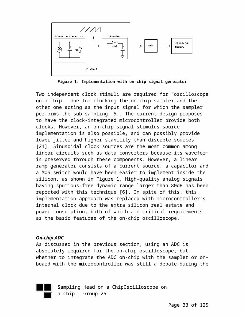
On-chip clock stimulus
Figure 1: Implementation with on-chip signal generator
Two independent clock stimuli are required for “oscilloscope on a chip”, one for clocking the on-chip sampler and the other one acting as the input signal for which the sampler performs the sub-sampling [5]. The current design proposes to have the clock-integrated microcontroller provide both clocks. However, an on-chip signal stimulus source implementation is also possible, and can possibly provide lower jitter and higher stability than discrete sources [21]. Sinusoidal clock sources are the most common among linear circuits such as data converters because its waveform is preserved through these components. However, a linear ramp generator consists of a current
Sampling Head on a ChipOscilloscope on a Chip | Group 25
Page 23 of 92
source, a capacitor and a MOS switch would have been easier to implement inside the silicon, as shown in Figure 1. High-quality analog signals having spurious-free dynamic range larger than 80dB has been reported with this technique [6]. In spite of this, this implementation approach was replaced with microcontroller’s internal clock due to the extra silicon real estate and power consumption, both of which are critical requirements as the basic features of the on-chip oscilloscope.
On-chip ADCAs discussed in the previous section, using an ADC is absolutely required for the on-chip oscilloscope, but whether to integrate the ADC on-chip with the sampler or on-board with the microcontroller was still a debate during the design cycle. There are several tempting advantages of having the ADC on-chip:
Reducing interconnections and loading effect Simplifying future automation and test integration for the customer Maximizing the return on test investment since the integrated test circuitry can
be use in all level of the system
However, using an on-chip ADC would inevitably increase the cost of fabrication for both the prototype and the customer, along with the increased risk and resources for the ADC to function properly. In short, if the ADC is placed on the chip, then the digital data needs to be transferred out of the chip to be analyzed, which may require additional circuitry. If it is off-chip, the analog signal will need to be brought out of the chip, which may increase noise and decrease accuracy, as well as the losing the advantages listed above. Since the minimum target set calls for the lowest silicon real estate possible, the idea of on-chip ADC will likely be dropped.
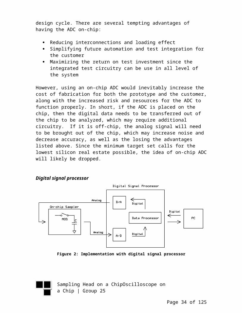
Digital signal processor
Figure 2: Implementation with digital signal processor
Sampling Head on a ChipOscilloscope on a Chip | Group 25
Page 24 of 92

Many data processing ICs such as digital signal processors (DSP) have both on-chip ADC and digital-to-analog converters (DAC) [21]. One idea is that the DSP can be implemented instead of the microcontroller to not only collect and translate the converted digital data, but to also perform additional features such as spectral analysis. First an ADC is tested using a calibration bias voltage. Then the DAC circuit is excited by streams of digital signals generated by the DSP, which is ultimately determined by the end user, to output the analog waveforms to the sampler. The sampled analog response is then cycled again into the ADC and collected by the DSP. Extending the currently planned implementation of the “on-chip oscilloscope” to include a DAC and a DSP is relatively straight forward, as shown in Figure 2. Even though adding a DAC would extend the feature of the on-chip oscilloscope and greatly increase the marketability of the entire system, it is too risky and beyond the bounds of the minimum target feature set.
Sampling Head on a ChipOscilloscope on a Chip | Group 25
Page 25 of 92
4. Top Level Description
Figure 3: Top level block diagram
Interface Type Voltage Current Description
5V Power Electrical – power 5V 500mA
(max)
The USB interface provides 5V to the on-chip oscilloscope from the PC’s power supply.
Sampler Input Signal
Electrical – analog
3.3V(max)
<1mA (max)
<1uA (typ)
This interface is the input signal to be sampled by the system. On the chip, the signal can be connected or disconnected from the sampler using a simple on-chip multiplexer.
Calibration Enable
(through USB)
Electrical – control
signal
3.3V (max)
<10uA (typ)
The calibration enable selects the calibration as the input to the on-chip sampler, as desired by the user. This control signal is transferred to the system from PC via USB.
Signal Output (USB)
Electrical – digital 5V 500mA
(max)
USB provides users a simple method of connecting the on-chip oscilloscope output to PC. The data is transmitted serially in packets through a differential pair.
Table 6: Top level interface description
Sampling Head on a ChipOscilloscope on a Chip | Group 25
Page 26 of 92

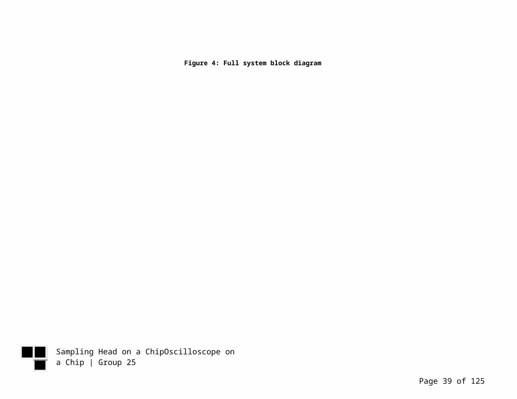
4.1 Block Diagram
Figure 4: Full system block diagram
Sampling Head on a ChipOscilloscope on a Chip | Group 25
Page 27 of 92
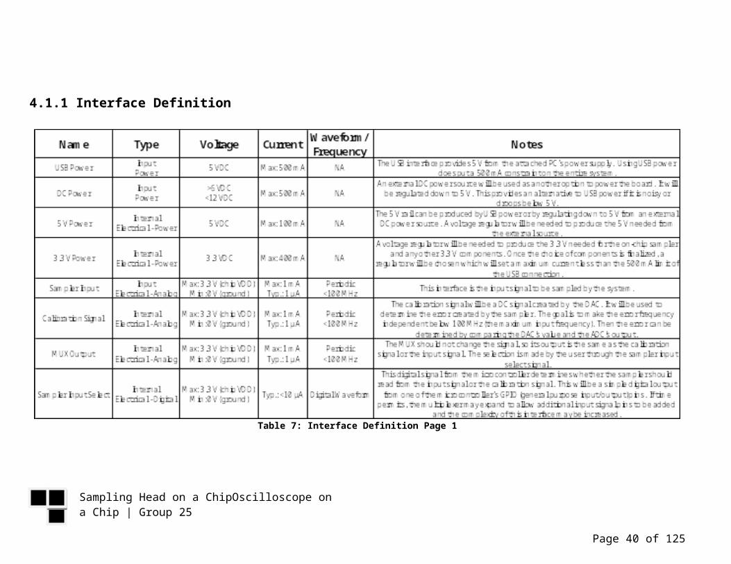
4.1.1 Interface Definition
Table 7: Interface Definition Page 1
Sampling Head on a ChipOscilloscope on a Chip | Group 25
Page 28 of 92
Table 8: Interface Definition Page 2
Sampling Head on a ChipOscilloscope on a Chip | Group 25
Page 29 of 92
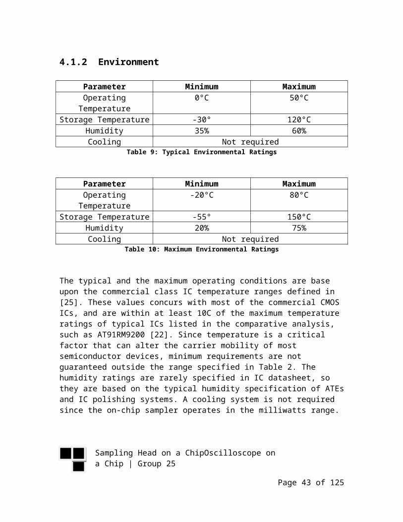
4.1.2 Environment
Parameter Minimum MaximumOperating Temperature 0°C 50°C
Storage Temperature -30° 120°CHumidity 35% 60%Cooling Not required
Table 9: Typical Environmental Ratings
Parameter Minimum MaximumOperating Temperature -20°C 80°C
Storage Temperature -55° 150°CHumidity 20% 75%Cooling Not required
Table 10: Maximum Environmental Ratings
The typical and the maximum operating conditions are base upon the commercial class IC temperature ranges defined in [25]. These values concurs with most of the commercial CMOS ICs, and are within at least 10C of the maximum temperature ratings of typical ICs listed in the comparative analysis, such as AT91RM9200 [22]. Since temperature is a critical factor that can alter the carrier mobility of most semiconductor devices, minimum requirements are not guaranteed outside the range specified in Table 2. The humidity ratings are rarely specified in IC datasheet, so they are based on the typical humidity specification of ATEs and IC polishing systems. A cooling system is not required since the on-chip sampler operates in the milliwatts range.
Sampling Head on a ChipOscilloscope on a Chip | Group 25
Page 30 of 92
5. Functional Unit Descriptions (Level 1)
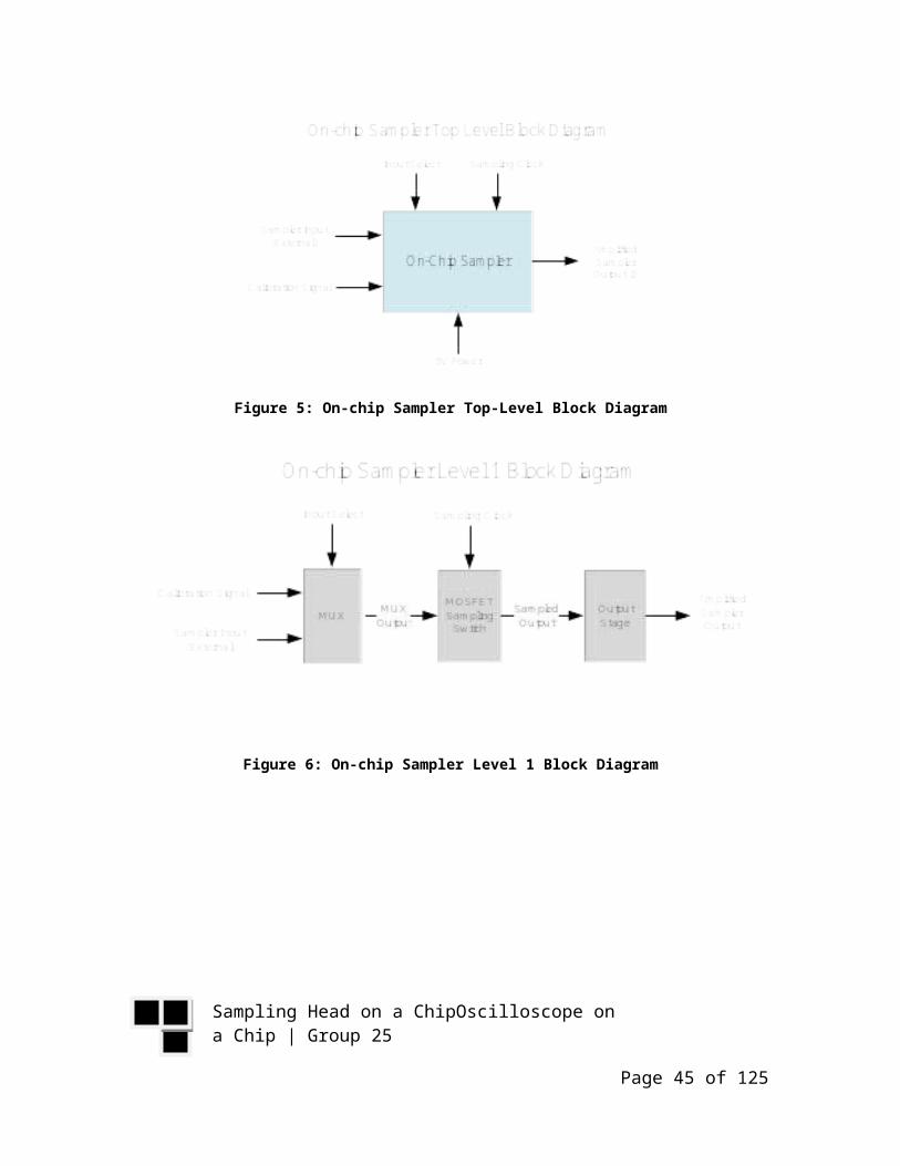
5.1. On-Chip Sampler Functional Block DiagramThe goal of the on-chip sampler is to periodically collect the analog voltage at the node of interest with minimum distortion. The minimum distortion, also known as non-intrusive testing, is one of the fundamental features of the Oscilloscope-on-a-Chip. In theory the sampler achieves this goal through reduced parasitic and down-sampling. Both of these are described in the functional unit description in Section 5.1.2.
Figure 5: On-chip Sampler Top-Level Block Diagram
Figure 6: On-chip Sampler Level 1 Block Diagram
Sampling Head on a ChipOscilloscope on a Chip | Group 25
Page 31 of 92
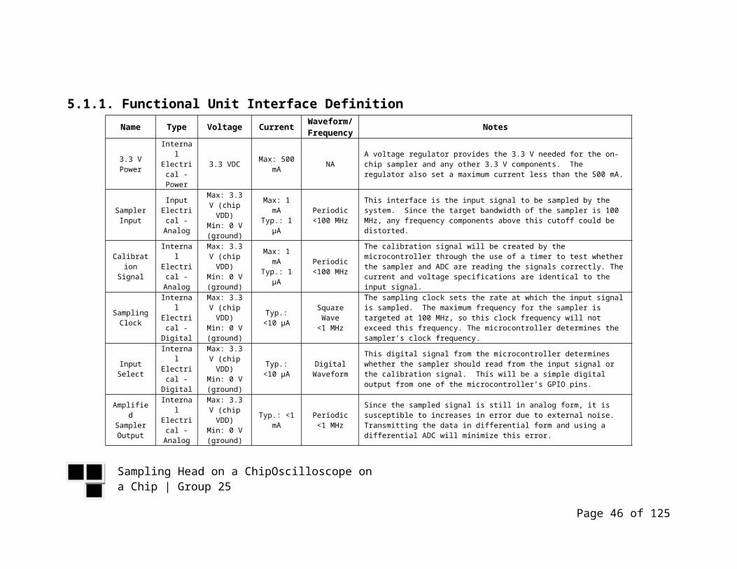
5.1.1. Functional Unit Interface DefinitionName Type Voltage Current Waveform/
Frequency Notes
3.3 V Power Internal
Electrical - Power
3.3 VDC Max: 500 mA NA A voltage regulator provides the 3.3 V needed for the on-chip sampler and any other
3.3 V components. The regulator also set a maximum current less than the 500 mA.
Sampler Input
InputElectrical -
Analog
Max: 3.3 V (chip VDD)
Min: 0 V (ground)
Max: 1 mATyp.: 1 µA
Periodic<100 MHz
This interface is the input signal to be sampled by the system. Since the target bandwidth of the sampler is 100 MHz, any frequency components above this cutoff could be distorted.
Calibration Signal
InternalElectrical -
Analog
Max: 3.3 V (chip VDD)
Min: 0 V (ground)
Max: 1 mATyp.: 1 µA
Periodic<100 MHz
The calibration signal will be created by the microcontroller through the use of a timer to test whether the sampler and ADC are reading the signals correctly. The current and voltage specifications are identical to the input signal.
Sampling Clock
InternalElectrical -
Digital
Max: 3.3 V (chip VDD)
Min: 0 V (ground)
Typ.: <10 µA Square Wave<1 MHz
The sampling clock sets the rate at which the input signal is sampled. The maximum frequency for the sampler is targeted at 100 MHz, so this clock frequency will not exceed this frequency. The microcontroller determines the sampler’s clock frequency.
Input SelectInternal
Electrical - Digital
Max: 3.3 V (chip VDD)
Min: 0 V (ground)
Typ.: <10 µA Digital Waveform
This digital signal from the microcontroller determines whether the sampler should read from the input signal or the calibration signal. This will be a simple digital output from one of the microcontroller’s GPIO pins.
Amplified Sampler Output
InternalElectrical -
Analog
Max: 3.3 V (chip VDD)
Min: 0 V (ground)
Typ.: <1 mA Periodic<1 MHz
Since the sampled signal is still in analog form, it is susceptible to increases in error due to external noise. Transmitting the data in differential form and using a differential ADC will minimize this error.
MUX Output
InternalElectrical - Analog
Max: 3.3 V (chip VDD)
Min: 0 V (ground)
Typ.: <1 µA Periodic<100 MHz
The multiplexer should not change characteristics of the input signal, so its output is the identical to either the calibration signal or the input signal. The selection is made digitally by the user through the sampler input select bit.
Sampler Output
InternalElectrical - Analog
Max: 3.3 V (chip VDD)
Min: 0 V (ground)
Typ.: <1 µA Periodic<1 MHz
The output of the sampling switch is fed through an output stage before it goes to an off-chip ADC. Since the output stage is a unity-gain buffer, the interface characteristics should stay the same from the sampling switch. The target frequency for the ADC input is 1 MHz
Table 11: Sampler Interface Definition
Sampling Head on a ChipOscilloscope on a Chip | Group 25
Page 32 of 92
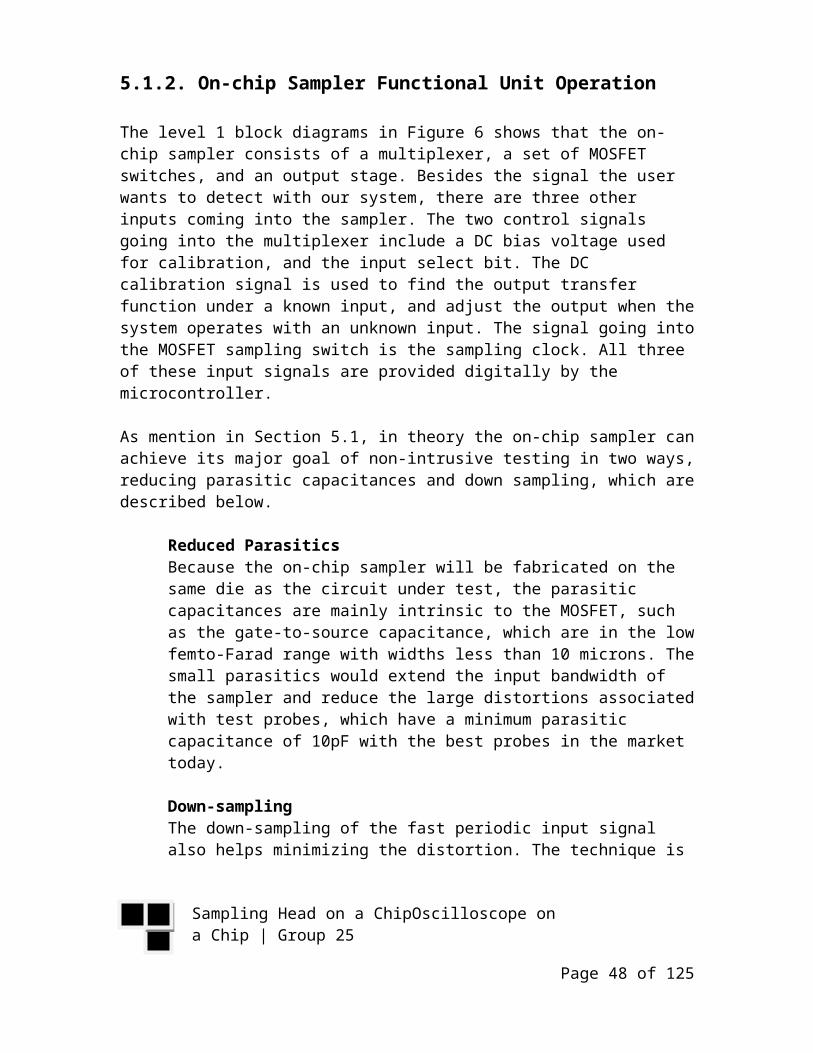
5.1.2. On-chip Sampler Functional Unit Operation
The level 1 block diagrams in Figure 6 shows that the on-chip sampler consists of a multiplexer, a set of MOSFET switches, and an output stage. Besides the signal the user wants to detect with our system, there are three other inputs coming into the sampler. The two control signals going into the multiplexer include a DC bias voltage used for calibration, and the input select bit. The DC calibration signal is used to find the output transfer function under a known input, and adjust the output when the system operates with an unknown input. The signal going into the MOSFET sampling switch is the sampling clock. All three of these input signals are provided digitally by the microcontroller.
As mention in Section 5.1, in theory the on-chip sampler can achieve its major goal of non-intrusive testing in two ways, reducing parasitic capacitances and down sampling, which are described below.
Reduced ParasiticsBecause the on-chip sampler will be fabricated on the same die as the circuit under test, the parasitic capacitances are mainly intrinsic to the MOSFET, such as the gate-to-source capacitance, which are in the low femto-Farad range with widths less than 10 microns. The small parasitics would extend the input bandwidth of the sampler and reduce the large distortions associated with test probes, which have a minimum parasitic capacitance of 10pF with the best probes in the market today.
Down-sampling The down-sampling of the fast periodic input signal also helps minimizing the distortion. The technique is based on sequential equivalent time sampling where a periodic waveform is reconstructed by sampling an identical periodic waveform at a different frequency. For example, if the sampling frequency is taken slightly less than the input frequency, the output frequency would be the difference between the two. Using a mathematical expression, then:
Equation 1
As one can see, the smaller the difference between the sampling and the input frequency, the slower is the output. A slower output also has higher resolution, but at the expense of the number of periods because more cycles are required to reconstruct one period of the original waveform.
Sampling Head on a ChipOscilloscope on a Chip | Group 25
Page 33 of 92
The output from MOSFET sampling switch is buffered through a unity-gain voltage follower before it is routed off-chip to an ADC. We chose to use single-ended signaling with one of the two signals being the ground. Even though there are advantages of using the common-mode noise rejection by the ADC, the output from on-chip sampler will be slow enough that the distortion on the line is insignificant. A brief description of the sub-block of the on-chip sample is written below, with directions to more detailed descriptions in Section 6.
MultiplexerThe multiplexer allows the user to select between the calibration signal and the input signal of interest. It consists of basic digital gates implemented with MOSFET transistors, and functions with an input select bit provide by the microcontroller. A more detailed description of the multiplexer circuit can be found in Section 6.1.
MOSFET Sampling SwitchThe MOSFET sampling switch is a transistor-level circuit that samples and holds the analog voltages at the desired clock frequency. This is achieved with NMOS transistors and capacitors. A more detail description of the sampling switch circuit can be found in Section 6.2.
Output StageThe output stage is used for boosting the output drive. It consists of a single-stage, single-ended operational amplifier (OPAMP) configured as a unity gain buffer. A more detailed description of the output stage can be found in Section 6.3.
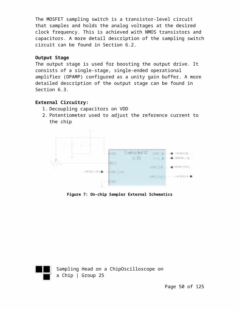
External Circuitry:1. Decoupling capacitors on VDD2. Potentiometer used to adjust the reference current to the chip
Figure 7: On-chip Sampler External Schematics
Sampling Head on a ChipOscilloscope on a Chip | Group 25
Page 34 of 92
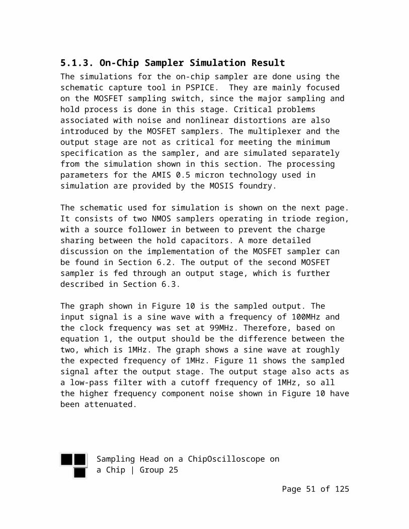
5.1.3. On-Chip Sampler Simulation ResultThe simulations for the on-chip sampler are done using the schematic capture tool in PSPICE. They are mainly focused on the MOSFET sampling switch, since the major sampling and hold process is done in this stage. Critical problems associated with noise and nonlinear distortions are also introduced by the MOSFET samplers. The multiplexer and the output stage are not as critical for meeting the minimum specification as the sampler, and are simulated separately from the simulation shown in this section. The processing parameters for the AMIS 0.5 micron technology used in simulation are provided by the MOSIS foundry.
The schematic used for simulation is shown on the next page. It consists of two NMOS samplers operating in triode region, with a source follower in between to prevent the charge sharing between the hold capacitors. A more detailed discussion on the implementation of the MOSFET sampler can be found in Section 6.2. The output of the second MOSFET sampler is fed through an output stage, which is further described in Section 6.3.
The graph shown in Figure 10 is the sampled output. The input signal is a sine wave with a frequency of 100MHz and the clock frequency was set at 99MHz. Therefore, based on equation 1, the output should be the difference between the two, which is 1MHz. The graph shows a sine wave at roughly the expected frequency of 1MHz. Figure 11 shows the sampled signal after the output stage. The output stage also acts as a low-pass filter with a cutoff frequency of 1MHz, so all the higher frequency component noise shown in Figure 10 have been attenuated.
Sampling Head on a ChipOscilloscope on a Chip | Group 25
Page 35 of 92
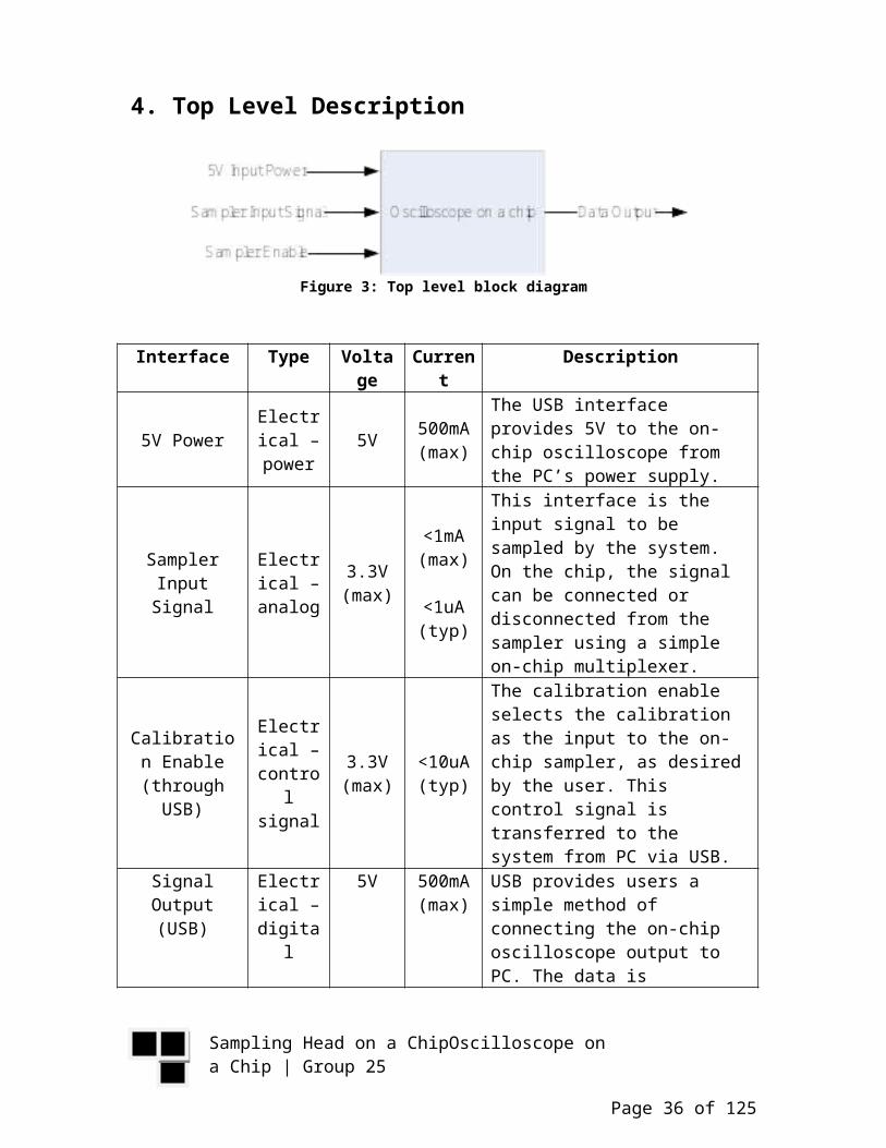
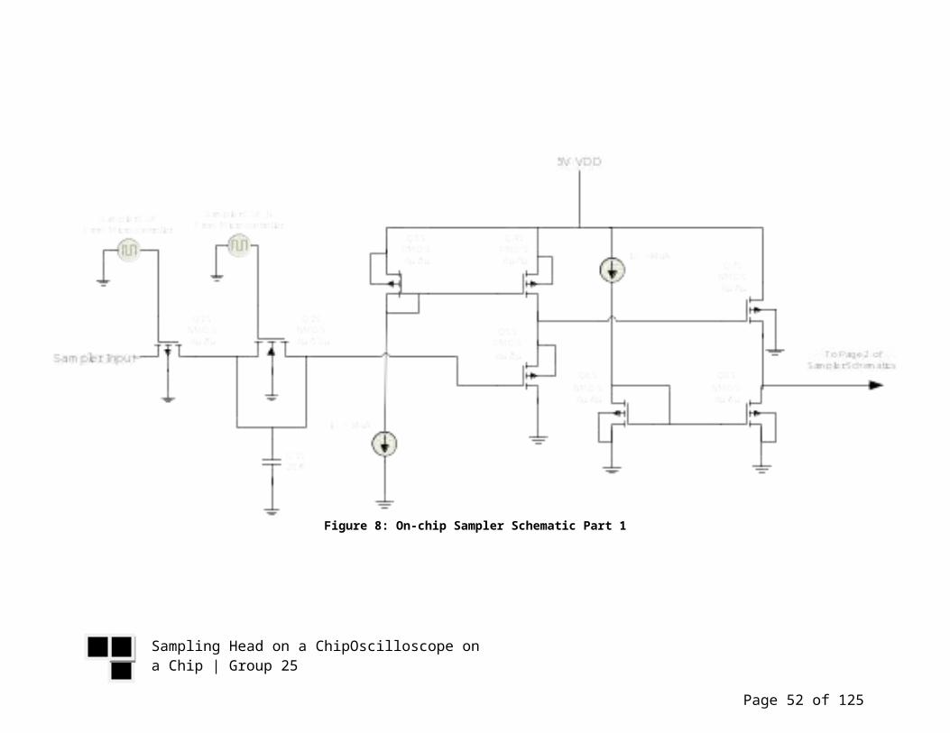
Figure 8: On-chip Sampler Schematic Part 1
Sampling Head on a ChipOscilloscope on a Chip | Group 25
Page 36 of 92

Figure 9: On-chip Sampler Schematic Part 2
Sampling Head on a ChipOscilloscope on a Chip | Group 25
Page 37 of 92
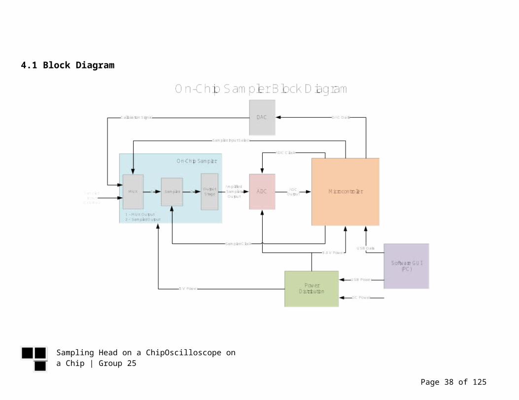
Figure 10: Unfiltered Sampler Output (Before Output Stage)
Figure 11: Filtered Sampler Output (After Output Stage)
Sampling Head on a ChipOscilloscope on a Chip | Group 25
Page 38 of 92
5.2. Analog to Digital Converter Functional Unit DescriptionThe Analog to Digital Converter (ADC) is the block that will convert the analog output signal from the sampler chip to a digital voltage value for processing in the microcontroller and software interfaces. Here are the main considerations in the design of the ADC circuitry:
1. Minimum of 6-bit resolution2. Minimum of 1 MSPS3. Serial SPI compatible output is preferred4. Low input current must be able to drive ADC5. Input voltage range must be at least 0-3V
Figure 12: ADC Block Diagram
Sampling Head on a ChipOscilloscope on a Chip | Group 25
Page 39 of 92
5.2.1 ADC Interface Definition
Table 12: ADC Interface Definition
Sampling Head on a ChipOscilloscope on a Chip | Group 25
Page 40 of 92

5.2.2 ADC Functional Unit Operation
Figure 13: ADC Schematics
Sampling Head on a ChipOscilloscope on a Chip | Group 25
Page 41 of 92

Analog to Digital Converter CircuitThe operations of the analog to digital converter can be effectively broken into the three major blocks as shown in the block diagram (Figure 5) and will be described as such.
Input Filter and BufferBefore entering the ADC, the output signal from the sampler chip must be properly conditioned and filtered to reduce noise and improve the sampling accuracy of the unit. After leaving the chip, the analog sampled signal will first pass though a buffer stage to prevent current draw from the chip and buffering the chip from external noise.
The part selected for the buffer stage was the LT 1632 Precision opamp. In the selection of a buffer opamp for this stage, it is imperative that the signal not be distorted and be passed though without any level shifting. This opamp has a 45 MHZ range which is well beyond the specs for the ADC input signal and has a voltage range of up to 45V, however it will only be tied to the 5V rail of our circuit due to the maximum voltage of the ADC input signal residing around 3.3V. The opamp is shown to be hooked in a unity gain configuration to allow the voltage to pass though adequately.
After the signal is buffered, it is sent though a low pass filter designed to attenuate noise above about 47Mhz. Due to the speed of the sampling that will be completed, it is imperative that the tolerance of both the resistor and the capacitor be low and introduce little distortion. The resistor chosen was a Metal film 51 ohm, 5% tolerance part. The composition of the resistor was picked over ordinary carbon due to the noise and distortion associated with carbon resistors. The capacitor chosen was a 47pf 10% tolerance NPO part. The NPO part was picked for the linearity it shows and because it was recommended in the datasheet of the ADC. This filter stage is essential in order to reduce any spiking noise and improve the accuracy if the analog to digital conversion.
Reference Voltage BufferThe range of the voltage that can be sampled by the ADC is set by the factory to be 2.5v. However, there is an option to overdrive this voltage up to VDD, which is what will be employed in order to get an input voltage of 3.3v. In order to do this, the 3.3 supply voltage will be buffered to limit the current and get rid of some noise using the same opamp buffer that was used for sampler buffering. This is convenient because the package of the buffer contain two opamps.
Also attached to voltage reference pin is a bypass capacitor of 10uf, used to ensure that the ADC remains stable. The capacitor was chosen to be a 10uf ceramic due to the lowered noise. Also another .1uf cap was put in parallel due to the noise benefits touted by the ADC datasheet.
Analog to Digital Converter Chip
Sampling Head on a ChipOscilloscope on a Chip | Group 25
Page 42 of 92
The LT1403 ADC chip was chosen for a variety of reasons. First, the sampling rate must be above about 1Mhz in order to adequately convert our input waveform. The LT1403 has a 2.8 Msps sampling rate allowing for the easy reconstruction of signals. Another important consideration in the selection of the ADC was the resolution. A 6-bit resolution was the required minimum and 8-bt would be desirable. This ADC has a 12 resolution, thus far exceeds our accuracy requirements. Perhaps the final important consideration driving our choice of this part was the serial output configuration. The serial interface to our microcontroller was determined to be SPI due to the ease of configuration and previous experience with the protocol. This ADC features a digital output that can be configured in SPI.
While the main deciding factors for the ADC were listed above, there were other benefits to choosing this part. The LT1403 contains sleep and nap function, allowing for the conservation of power, and the overdrive function allowing for the increase of the voltage range.
In order configure the LT1403 to run in an SPI interface, the part must receive a clock and enable signal from the microcontroller. The clock signal will be fed into the SCK (serial clock) input, and the enable for each word will be fed into the CONV (Conversion Start) input. The digital output will then flow out of the SDO (Serial Data Out) pin and into the microcontroller for further processing.
Sampling Head on a ChipOscilloscope on a Chip | Group 25
Page 43 of 92

5.3 Microcontroller Functional Unit DescriptionRequirements and Function:The microcontroller acts as the coordinator for the entire system. It interprets the user’s input, causes the system to perform the correct action, and then transmits the results back to the user on the computer. Here are the tasks the microcontroller is required to perform:
1. Receive and interpret user input2. Provide control signals/clock to the on-chip sampler3. Provide control signals/clock to the A/D converter4. Provide control signals/clock to the D/A converter for calibration5. Receive and store results from the A/D converter (including calibration results)6. Use calibration results to correct for error7. Transmit the results to the user
This project has unusual requirements for a microcontroller. The high speed of the sampler and A/D converter will require a fast microcontroller even though the system itself contains only a few devices and interfaces. Since the A/D converter will run at speeds greater than 1 MHz, the microcontroller must be able to operate at high enough speeds to receive this data. The ideal microcontroller would have a low pin count, be simple to program, but be capable of moving and processing large quantities of data at high speeds. The microcontroller also had limits on power consumption, packaging, and cost. Here is a detailed list of these specifications:
1. Processor clock speed: >20 MHz2. Power consumption: <500 mW (limited by USB power specifications)3. Cost: <25$ (limited budget)4. Packaging: no BGA or QFN packages5. Pin Count: <100 (to simplify construction)6. Data Memory: > 16 Kbyte (for storing sampled data)7. USB hardware interface8. Free software tools
Below is a list of helpful, but not mandatory, features for the microcontroller block:
1. Direct memory access (reduces processor overhead receiving data)2. Capable of producing clocks up to 100 MHz with 1 MHz resolution (using either
timers, pulse width modulation blocks, system clocks, or phase locked loops)3. Interface with A/D converter can operate without processor intervention4. High speed USB hardware interface5. Operates off one voltage rail (preferably 3.3 V)6. Moves multiple bytes per instruction
Sampling Head on a ChipOscilloscope on a Chip | Group 25
Page 44 of 92
Best Solution:The most familiar microcontrollers to our group are Atmel’s line of 8-bit AVR microcontrollers. Unfortunately, these products have trouble meeting our requirements. They run at low speeds (< 16 MHz) and only process one byte per instruction. Also, the only AVR microcontrollers with a USB interface are around $20.However, our familiarity with Atmel led to an investigation of Atmel’s line of ARM7 (AT91SAM7S) products. These microcontrollers operate at speeds up to 55 MHz, contain a USB interface, and cost only around $10 per part. They seemed a better fit for our design, which may require higher speeds. Also the packaging is a 64-pin quad flat pack (QFP) package, which will result in a simpler design and construction.The problem with these microcontrollers is obtaining hardware and software tools to assist in programming. Investigation has shown that open source compilers are available and Atmel offers free software to assist in programming the devices. From this information, programming these microcontrollers should not be a problem.
Sub-block Diagram:Like any microcontroller, the AT91SAM7S has a processor core and various peripheral devices. The following block diagram gives a visual representation of these peripheral devices will be utilized. Detailed descriptions can be found in the sections following the block diagram.
Figure 14: Microcontroller Block Diagram
Sampling Head on a ChipOscilloscope on a Chip | Group 25
Page 45 of 92
5.3.1. Microcontroller Interface Definition
Table 13: Microcontroller Interface Definitions Page 1
Sampling Head on a ChipOscilloscope on a Chip | Group 25
Page 46 of 92
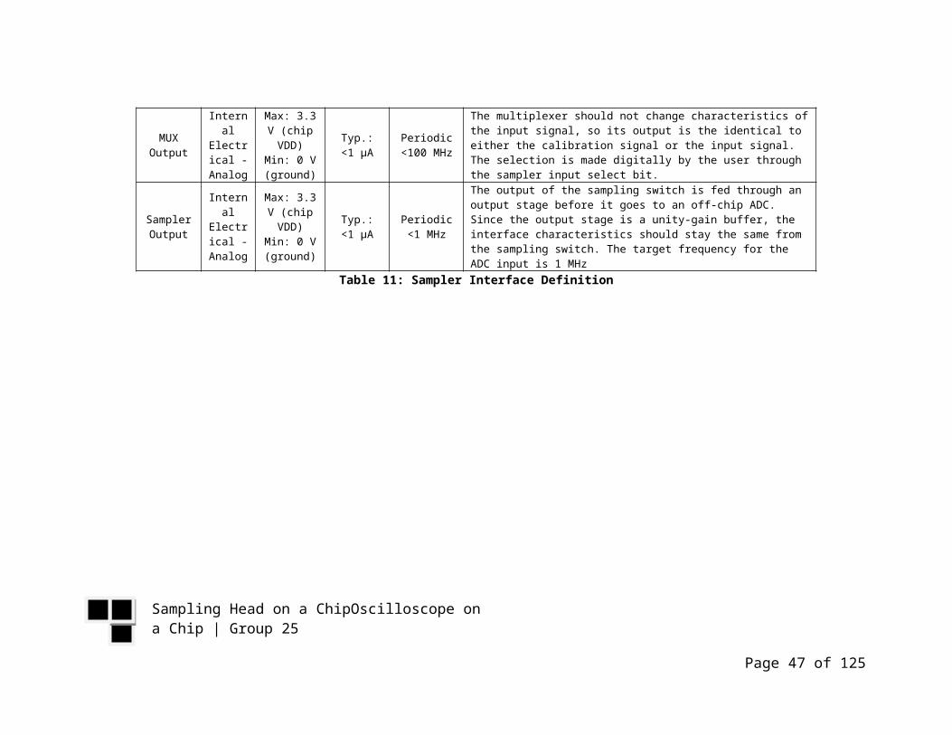
Table 14: Microcontroller Interface Definitions Page 2
Sampling Head on a ChipOscilloscope on a Chip | Group 25
Page 47 of 92
5.3.2. Microcontroller Hardware OperationPower:AT91SAM7S chips have a number of power pins. The I/O pins can operate off 3.3 V, but the majority of the hardware uses 1.8 V. The package contains a built-in 1.8 V regulator that converts 3.3 V to 1.8 V for the core. The design will make use of this regulator. Decoupling capacitors are also needed near every power pin.
Processor Core:The ARM7 core is a surprisingly powerful processor for such an inexpensive chip. ARM stands for advanced RISC (reduced instruction set computer) machine. The ARM instruction set has fewer than 60 instructions, so this truly is a RISC processor.The maximum clock frequency for this processor core is 55 MHz. Combined with the fact that it operates on 32-bit words at about one instruction per cycle, the processor could potentially move about 12 times as much data per second as a 16 MHz 8-bit AVR processor. This will allow the processor to keep up with the data it is receiving from the A/D converter. Also, some error correction will need to be done on the data before transmitting it to the user, requiring more processing capacity.
A quick calculation shows that a 55 MHz processor would have 55 instructions per every 1 MHz A/D converter cycle, which is plenty to just read and store the data to memory. However, to increase the signal resolution, the A/D converter will have the capability of running up to 10 MHz, which would be a maximum of only 5.5 instructions per cycle. This would be close to creating a bottleneck.
The Serial Peripheral Interface and Direct Memory Access:The solution to this bottlenecking problem for high speed A/D conversion is to use the serial peripheral interface (SPI) with direct memory access (DMA). The SPI interface is capable of running in an autonomous mode where it automatically initiates a transaction at a set frequency. This means once setup, the SPI interface can communicate with the A/D converter without processor overhead.
DMA is the other half of this solution. It allows the SPI interface to place the data it receives into data memory without the processor’s intervention. A starting and ending point in memory are set, and then the DMA controller automatically stores data and increments the current memory location. The problem is that DMA does not work with the general purpose I/O pins (GPIOs – the standard I/O pins on the microcontroller). This means the A/D converter must interface through SPI to make use of DMA.Using SPI and DMA effectively eliminate the speed constraint on the processor, so using these features would allow the processor to run at slower speeds. Unfortunately, none of the slower AVR microcontrollers contain a DMA controller.
Sampling Head on a ChipOscilloscope on a Chip | Group 25
Page 48 of 92
System Clocks:The input clock to the system will be a 16 MHz crystal. An on-chip oscillator can then be connected to the crystal to create a 16 MHz clock. The microcontroller also contains a phase locked loop (PLL) capable of clock multiplication. This PLL needs an external RC filter to function properly.
This PLL will multiply the 16 MHz clock by twelve to 192 MHz. This is the master clock. While it cannot exceed 220 MHz, it can be faster than the processor’s maximum clock of 55 MHz. The USB interface requires a 48 MHz clock, so the master clock will be divided by four. 48 MHz is also a suitable clock for the processor core, so the core’s clock will also be the master clock divided by four.
The benefit of using a 196 MHz master clock is that the peripherals like timers, PWMs, and the SPI interface can run at this higher clock speed. A 196 MHz 8-bit SPI could perform read from a 24 MHz A/D converter. This high speed also allows the timers and PWMs to create high speed clocks for the sampler. If testing shows that these high speed clocks are unnecessary, we will reduce the frequency to save power.
USB Interface:The USB interface is a potentially challenge in our design. The AT91SAM7S creates a full speed USB device that runs off a 48 MHz clock and is capable of transferring 1.5 Mbps. The largest difficulty is initializing it as a device recognizable to the computer, but sample code exists to assist in this problem. Once the interface is initialized and the microcontroller is enumerated by the computer, data transfer is done via a buffer. Outgoing data is written into the buffer and transmitted at the next opportunity. Incoming data is also stored to a buffer where it can be read when the processor is available. Interrupts are also triggered when data is received to assist in receiving commands from the computer.
Some external hardware is needed for the USB interface. First 5 V USB power is connected to a GPIO set in input mode through a voltage divider (to divide 5 V to 3.3 V) to detect when USB is connected. Another GPIO set as an output will control a MOSFET that can enable/disable a pull-up. The pull-up allows the microcontroller to disable the pull-up when the bus is not connected to save power and also decide when the device can be connected by the computer.
As a note, if difficulties are encountered with USB, the AT91SAM7S contains UARTs that can interface with a computer through the serial port at lower speeds.
Sampling Head on a ChipOscilloscope on a Chip | Group 25
Page 49 of 92
Clock Generation:Clock generation could require additional hardware as the microcontroller’s timers and PWMs have limited frequencies they can output. Because of how these devices work, the output clock can only be a frequency that the master clock is a multiple of. This means the highest frequencies that could be produced are 192 MHz, 96 MHz, 64 MHz, and 48 MHz. Since the sampler’s clock and input signal must be within 1 MHz of each other, this limitation presents a problem. At the current time, the microcontroller’s clock generation capabilities will only be used for demonstrations and will run at lower frequencies where the timers can generate two frequencies within 1 MHz of each other.
Control Signals & GPIOs:Creating control signals will be done by setting the values of the microcontroller’s GPIOs. This is done by writing to registers that control the state of these GPIOs. The signals going to the sampler need to be level shifted from 3.3 V to 5 V. The simplest method to accomplish this is to use these GPIOs in their open drain mode and then pull the line up to 5 V. The microcontroller can take 5 V at a pin and remain within specification, but cannot source 5 V. Using the pins in open drain mode allows the pin to be high impedance when it outputs a one, allowing the pull-up to bring it up to 5 V.
Programming:Programming the microcontroller could be an area of the design that causes some problems. On-line documents from Atmel indicate that the microcontrollers come with bootloader software that allows them to be programmed through USB. Open source software does exist to compile the program and free Atmel software exists to interface with the bootloader.
Sampling Head on a ChipOscilloscope on a Chip | Group 25
Page 50 of 92
5.3.3. Microcontroller Schematic Diagram
Figure 15: Microcontroller Schematic Diagram
Sampling Head on a ChipOscilloscope on a Chip | Group 25
Page 51 of 92
5.3.4. Microcontroller Firmware Operation
The firmware programming will be done in C and then compiled into the ARM7 instruction set. Programming will be done through USB using the default boot loader.
Initialization:Initialization is a straight forward process. The microcontroller begins by initializing the clocks to ensure everything is operating at the correct speed. Then it initializes I/O port directions and values and begins initializing the various peripherals that are used.
1. Initialize clocks2. Initialize I/O ports3. Set default port values4. Initialize USB5. Ensure USB is connected, otherwise wait until it is connected6. Initialize SPI7. Initialize timers/PWMs for clocks8. Enter main loop
User Commands:Any command sent by the user over USB will trigger an interrupt causing the command to be processed. The microcontroller will interpret the command and perform the correct operation. The actions could include changing the value of a GPIO control signal, starting data collection, start calibration, or changing a clock’s frequency.
Figure 16: User Command Code Flow Chart
Sampling Head on a ChipOscilloscope on a Chip | Group 25
Page 52 of 92

Calibration:Calibration is performed by sweeping the input range of the sampler with a DC voltage produced by a DAC and then reading the sampler output at this voltage. Below is a flow chart of the calibration code:
Figure 17: Calibration Code Flow Chart
Sampling Head on a ChipOscilloscope on a Chip | Group 25
Page 53 of 92
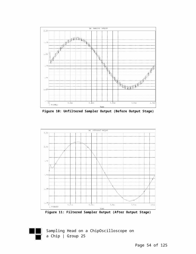
Sampling:Sampling is done by initializing SPI and DMA to run automatically and then waiting for the sampling process to complete. The microcontroller’s core is free during this time to perform other tasks. Upon completion the microcontroller performs error correction and then sends the data over USB.
Figure 18: Sampling Code Flow Chart
Sampling Head on a ChipOscilloscope on a Chip | Group 25
Page 54 of 92

Error Correction:Error correction is completed by looping through the data and using the information gathered during calibration to subtract out the error. For example, if during calibration an ADC value of 120 corresponded to a DAC value of 130, then any sampled data reading 120 is corrected to 130. Below is a flow chart of the error correction algorithm.
Figure 19: Error Correction Code Flow Chart
Sampling Head on a ChipOscilloscope on a Chip | Group 25
Page 55 of 92
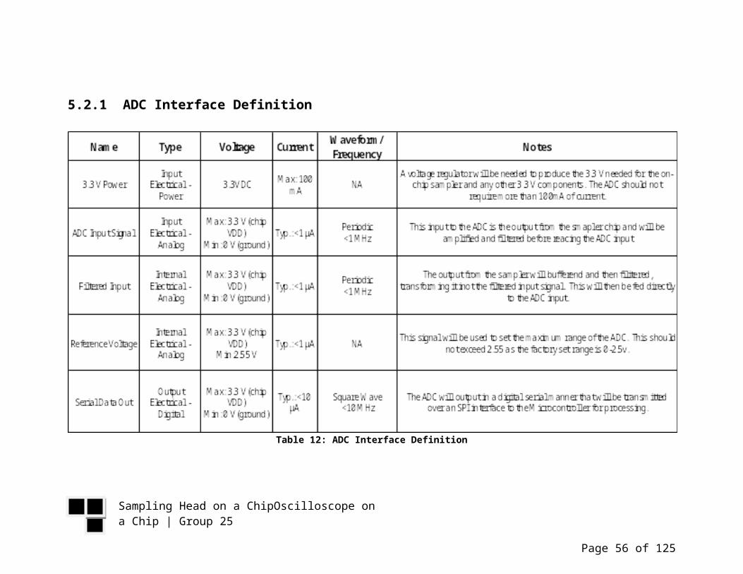
5.4. Digital to Analog Converter Functional Unit Description
Figure 20: Digital-to-Analog Converter Block Diagram
5.4.1. Digital to Analog Converter Interface Definition
Name Type Voltage Current Waveform/Frequency Notes
Microcontroller SPI Input
InternalElectrical -
Digital
HIGH: 5VLOW: 0V Typ.:< 1 µA N/A
The MCP4921 DAC will interface with the microcontroller using Serial Peripheral Interface (SPI) port. It is a 3-wire digital serial interface, but is only unidirectional. Definition of each of the three pin are explained below.
Chip Select (CS)Internal
Electrical - SPI
HIGH: 5VLOW: 0V Typ.:< 1 µA N/A
This is the chip select input. It requires an active LOW signal to enable serial clock and data to function.
Serial Clock (SCK)
InternalElectrical -
SPI
HIGH: 5VLOW: 0V Typ.:< 1 µA Digital
16MHz
SCK is used to synchronize the input data. Data are clocked-in on each rising edge of this pin.
Serial Data (SDI)
InternalElectrical -
SPI
HIGH: 5VLOW: 0V Typ.:< 1 µA N/A
Commands and data are sent through this pin in 16-bit words, for which the lower 12 bit are the DAC data bits and the upper four are the configuration bits.
Reference Voltage
InternalElectrical -
Analog
Typ: 4.096V Typ.: <1 µA N/A
The reference voltage is responsible for setting the maximum output voltage. Each digital input would represent a fraction of the reference, and the corresponding analog level would be created at the output.
Analog OutputInternal
Electrical - Analog
Max: 5 V (VDD)
Min: 0 V (ground)
Typ.: <1 µA N/A
The analog output is fed to the on-chip sampler for calibration. Since the DAC is 12 bits and the reference is set at 4.096V, the precision of the DC bias is approximately 1mV for each least significant bit.
Table 15: Digital to Analog Converter Interface Definition
Sampling Head on a ChipOscilloscope on a Chip | Group 25
Page 56 of 92
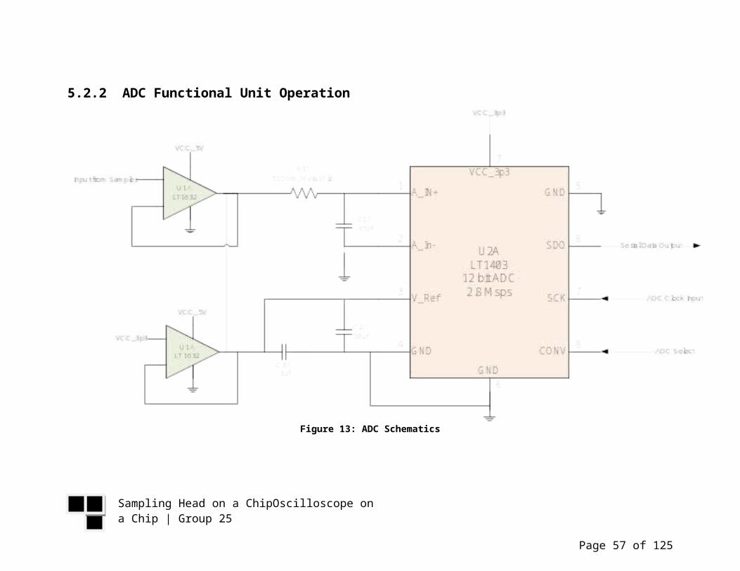
5.4.2. Digital to Analog Unit Operation
Figure 21: Digital-to-Analog Converter Schematic
Since the microcontroller can only output digital serial bits, and the calibration signal for the on-chip sampler requires an analog bias voltage, a digital-to-analog (DAC) converter is needed for the calibration to function. The currently purposed DAC for our system is MCP4921 manufactured by Microchip. It is a 12-bit DAC implemented using resistive string architecture with SPI protocol. The MCP4921 DAC operates from 2.7V to 5.5V, which fits well with both the 3.3V and the 5V rail voltages provided by our system. The MCP4921 also has an Output Power Down Control (SHDN) feature that ensures high impedance when first powered up. Another extra feature of this DAC is the Latch DAC Input (LDAC). A LOW input on this pin transfers the input latch registers to the DAC registers. Since we are not interested on the exact timing when changing the bias voltage, this input pin is always tied to LOW so that the interface with the microcontroller is reduced from four to three.
For an ideal DAC, the least significant bit output analog voltage is directly related to the reference voltage with the following expression:
, where G is the output gain and DN is the digital input value
Equation 2
Therefore, with a 12 bit precision and a reference voltage of 4.096V, each least significant bit change represents a 1mV change at the output. Since the output is used only for calibrating the on-chip sampler, which is fed into a 12-bit ADC, a 1mV precision matches well with our system for the voltage range within our interest. In this design, we used a voltage reference source, LM4040, for providing the 4.096V reference. The
Sampling Head on a ChipOscilloscope on a Chip | Group 25
Page 57 of 92

voltage source requires a quiescent reverse current between 65uA and 15mA to operate, and using a 1kΩ would allow approximate 1mA of constant current to flow through both the reference and the load.
The standard SPI interface allows for easy writing of command with the ARM7 microcontroller. The writing command is initialized by first setting the chip select input (CS) LOW, and then write out a 16-bit word to the serial data input (SDI). The lower 12 bits represents the DAC data and the upper four are used for DAC configuration. A diagram of the write command register is shown below.
Write Command RegisterD15 D14 D13 D12 D11-D0N/A BUF GA SHDN 12 bit DAC data
Bit15 Bit0
Bit 14: Reference Voltage Input Buffer Control BitWe will set this bit LOW to disable the input buffer. The un-buffered input has an input resistance of 165kΩ, which is about 100 times the resistor we are using to set the reference.
Bit 13: Output Gain Select BitWe will set high bit HIGH for unity output gain.
Bit 12: Output Power Down Control BitThis bit is default to LOW, which makes the output impedance, when device is first powered on. We will need to set this bit HIGH with each valid write command.
Bit 11 - Bit 0: DAC Data BitsThis is the 12 bit number that sets the analog output voltage. The binary value should represent a number between 0 and 4095.
Sampling Head on a ChipOscilloscope on a Chip | Group 25
Page 58 of 92
5.5. User Interface Functional Unit DescriptionThe user interface will be graphical in nature. It will be programmed in a GUI language such as Visual Basic or C#. This portion of the project will use an open source driver and may require programming in other languages to ensure the GUI can interface with the driver.
Figure 22: User Interface Block Diagram
5.5.1. User Interface Definitions
Table 16: User Interface Definition
5.5.2. User Interface Functional Unit OperationDevice Detection & Enumeration:To operate the system, the board must be connected to a computer through a USB port. The user interface then allows the user of the computer to send commands to and receive commands from the board via the microcontroller. When a USB device is connected to a USB port, the USB host in the computer detects the pull-up resistor on the positive line on the board. This tells the computer a device is connected and it begins enumerating that device. If a driver is available for that device, then the computer uses that driver. In this case, the device will not be a standard type. This results in Windows being unable to communicate with it. If the user starts up the user interface (UI), the program will begin by searching for a device of the correct type. The
Sampling Head on a ChipOscilloscope on a Chip | Group 25
Page 59 of 92

UI will use an open source USB driver capable of communicating with any USB device. Once the device has been detected and enumerated, normal USB communication can begin.Device Settings:Before issuing a command, the user can modify the settings of the device. These settings include:
External signal enable/disable External sampler clock enable/disable Internal signal frequency Internal sampler clock frequency A/D converter sampling frequency Samples per sampling command
The enable/disable settings will be set using command buttons. Clicking on them will toggle the corresponding setting. The other settings will be controlled by slider bars since the options be limited to frequencies that the microcontroller can produce. Labels will display the current settings on screen.
User Commands:Three commands can be transmitted to the on-board microcontroller:
Change setting Calibrate Sample
The actions taken by the microcontroller for these actions are listed in section 5.3. The GUI only needs to transmit the command over USB and wait for a response. In the case of a setting change, the microcontroller will answer with the changed setting to confirm that it made the requested change.
For calibration, the microcontroller will respond when it receives the command. Then the GUI will block all user input until the microcontroller sends another message saying it has finished calibration and is ready for additional tasks. If the microcontroller does not respond in a timely manner, the GUI will display an error and try to reestablish communication with the microcontroller.
For sampling, the microcontroller will respond that it is starting sampling. Like calibration, this will disable user input until the microcontroller responds again. This response will include transmitting all of the gathered data to the computer where the GUI can receive and store it. This information can then be exported as a text file or a MatLab file.
Sampling Head on a ChipOscilloscope on a Chip | Group 25
Page 60 of 92
Figure 23: Preliminary GUI Layout
Sampling Head on a ChipOscilloscope on a Chip | Group 25
Page 61 of 92
5.6. Voltage Regulator Functional Unit DescriptionThe voltage regulator serves the function of providing clean and regulated power to all the parts on the board. The two voltage rails needed are 3.3V and 5V. The following are the requirements for this voltage regulation solution:
1. Provide a 5V and 3.3V power rails at 500mA2. Decouple rails to counteract all noticeable noise3. Insert safety equipment to prevent reverse bias issues4. Allow the input to switch between a power supply, wall power, and USB power5. Use though hole parts for ease of prototyping
Figure 24: Voltage Regulator Block Diagram
Sampling Head on a ChipOscilloscope on a Chip | Group 25
Page 62 of 92
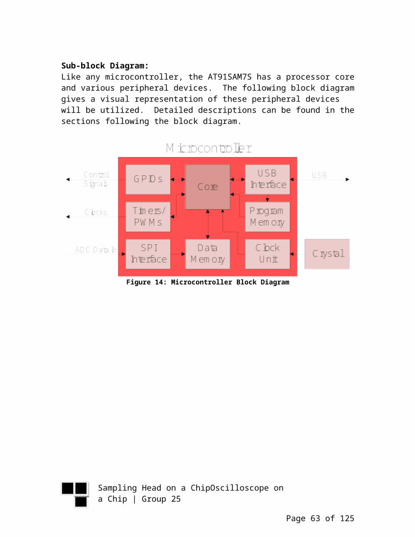
5.6.1 Voltage Regulation Interface Definition
Table 17: Voltage Regulator Interface Definition
Sampling Head on a ChipOscilloscope on a Chip | Group 25
Page 63 of 92
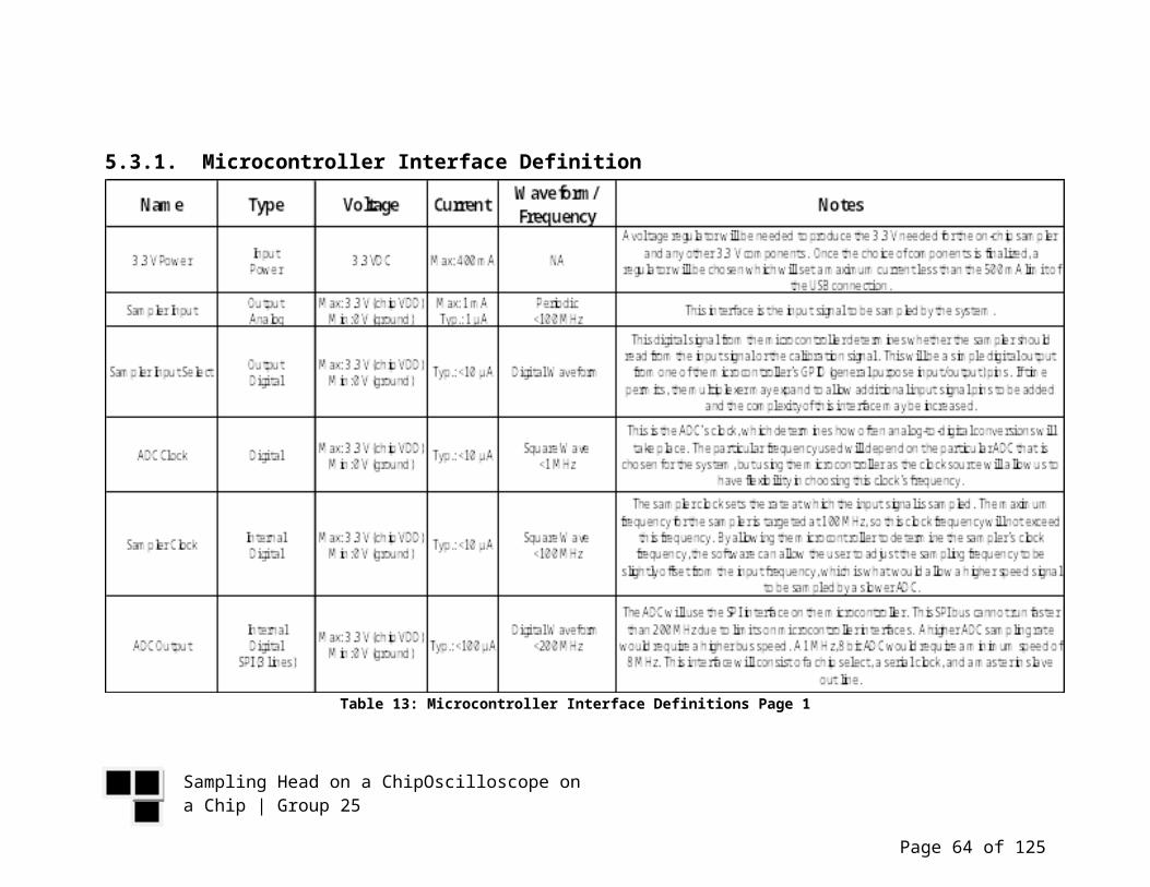
5.6.2 Voltage Regulation Functional Unit Operation
Figure 25: Voltage Regulator Schematics
Sampling Head on a ChipOscilloscope on a Chip | Group 25
Page 64 of 92

Voltage Regulation OverviewThe voltage regulator will provide power to the rest of the circuit as either 5V or 3V rails. This regulation circuitry has the option of pulling power from a USB source, a wall power input or power supply input depending of the jumper settings of the user. The operations of the voltage regulator circuit can be effectively broken down into three main blocks as shown in the block diagram, and will be described as such.
5V RegulatorIn this board, it was imperative that there be multiple power options in case one fails or the flexibility is needed (at exhibition for example). This flexibility was provided by the choice between the wall input, power supply input, and USB input. While the USB input is set to 5V (with some swing) the power supply and wall adapter could range from 6-20 volts. This required the use of a low dropout regulator to provide a clean 5V source to the circuit. The regulator that was chosen was the LM2937 due to reliability, input voltage range, and cost. In order to maintain stability on the regulator, a 10uf, low equivalent series resistance (ESR) capacitor was needed. The input also has a .1uf capacitor to dissipate noise before reaching the regulator. Attached to the input of the regulator circuitry is a schottky diode to prevent the user from damaging circuitry by revere biasing any power inputs. Another reliability measure added to this circuit is the decoupling capacitors placed on all of the voltage lines in the VR to dissipate major noise power.Power Input SwitchTo select between the USB power, wall power, and power supply power, it was important that there be a way of manually switching on the board. Our solution was to use jumpers base on the ease of use and the fact that there will never be a point in time where all power inputs are on. Also added to this switching circuit are LED’s that will identify which of the power inputs are available for the user. In our design, the green LED will light up when the user has plugged in a USB adapter and USB power is ready for use. The Red LED will light up when wall power or a power supply is plugged in and ready for use.3.3 Voltage regulatorIn order to obtain a 3.3 voltage rail, it was necessary to regulate our 5V rail down with a voltage regulator. The regulator used in this design is the LM2937-3.3. It is linier and limits the output current to 500mA, which is enough current for the systems that will be running off the 3.3 volt rail. This though-hole part has relatively low noise and ripple rejection features. In order for this circuit to remain stable, a capacitor must be placed on the output and due to the low ESR requirements of the LM2937-3.3, a low impedance 10uf electrolytic capacitor was chosen. Another small .1uf capacitor is placed physically close to the input pin of the LM2937-3.3 in order to reduce noise caused by potentially long traces. This 3.3 volt rail should feed directly to the ADC and parts of the microcontroller.
Sampling Head on a ChipOscilloscope on a Chip | Group 25
Page 65 of 92
6. Functional Unit Descriptions (Level 2)
6.1. Multiplexer Block Diagram
Figure 26: On-chip Multiplexer Level 2 Block Diagram
6.1.1. Multiplexer Interface DefinitionThe five input and output signals for the multiplexer are Input Select, Sampler Input, Sampling Clock, Calibration Signal, and Multiplexer Output. These five signals are identical to the ones listed under the same names in the Level 1 Interface Definition in Table 11, and thus are not listed in the following table.
Name Type Voltage Current Waveform/Frequency Notes
Sampled Input
InternalAnalog
Max: 3.3 V (chip VDD)
Min: 0 V (ground)
Typ.:< 1 µA N/A
This is the sampled input signal voltage levels to be stored into the hold capacitor. The signal will follow the input until the arrival of each clock falling edge, thus it is not periodic in nature. Its range shall be between ground and 3.3V.
Sampled Calibration
InternalAnalog
Max: 3.3 V (chip VDD)
Min: 0 V (ground)
Typ.: <1 µA N/A
This is the sampled calibration voltage levels to be stored into the hold capacitor. Since the calibration signal is a DC bias voltage, this signal is not periodic. Its range shall be between ground and 3.3V.
Digital Interfaces
InternalDigital HIGH: 3.3V
LOW: 0VTyp.: <1 µA N/A
Since the multiplexer is used to enable and disable the sampler clock for both the input signal and calibration, it should have the same characteristics as the sampling clock
Table 18: Multiplexer Level 2 Interface Definition
Sampling Head on a ChipOscilloscope on a Chip | Group 25
Page 66 of 92
6.1.2. Multiplexer Unit OperationThe multiplexer is implemented inside the on-chip sampler to provide the choice between the calibration and the actual input signal. Figure 24 shows the gate-level diagram of the multiplexer with an input select bit. It is implemented with standard logic gate components, with a total of two NAND gates and three inverters. A logic table showing the output based on the input is listed in Table 19. Whether the input select bit is HIGH or LOW, one of the two NAND gates will be ON and the other one OFF, thus switches between the calibration and the actual. The NAND gates are used because they are simpler to implement than their AND and OR counterparts using CMOS technology. The circuit-level implementation for the input sampler, the calibration sampler and the hold capacitor are discussed in Section 6.2.
Input Select Bit MUX Output0 Calibration1 Sampler Input
Table 19: Multiplexer Output versus Input Select Bit
CMOS Inverter and NAND Gate ImplementationFigure 25 shows the transistor-level schematics for implementing both the NAND gate and the inverter in the CMOS technology. This design cannot be broken down further because the layout would determine the specific parameter for fabrication. In order to minimize delay, the most important design parameter is the width-to-length ratio, which is different for PMOS and NMOS because of their difference in mobility. SPICE simulation results would show the exact width-to-length ratios for all the transistors.
Figure 27: CMOS Implementation of the Inverter and NAND Gate
Sampling Head on a ChipOscilloscope on a Chip | Group 25
Page 67 of 92

6.2. MOSFET Sampling Circuit Functional Unit Description
Figure 28: MOSFET Sampling Circuit Level 2 Block Diagram
6.2.1 MOSFET Sampling Circuit Interface DefinitionThe inputs and outputs including the Sampling Clock, the MUX Output and the Sampler Output have all been described in Table 11. To avoid repeating the identical interface description, the follow table, Table 20, only shows definitions that are specific to the Level 2 MOSFET sampling circuit.
Name Type Voltage Current Waveform/Frequency Notes
1 – Stage One Output
InternalElectrical -
Analog
Max: 3.3 V (chip VDD)
Min: 0 V (ground)
Typ.: <1µA Periodic<1 MHz
This interface sits between the first stage of the two sample-and-hold circuits and the buffer stage. The characteristic of the signal depends on the input and the calibration signal. The frequency of the waveform is based on the difference in speed between the sampling clock and the input signal.
2 – Stage Two Output
InputElectrical -
Analog
Max: 3.3 V (chip VDD)
Min: 0 V (ground)
Typ.: <1µA Periodic<1 MHz
This is the interface between the buffer stage and the second sample-and-hold circuit. Its properties are identical to that of stage one output because the buffer stage is consisted of only two source followers.
Table 20: Multiplexer Output versus Input Select Bit
Sampling Head on a ChipOscilloscope on a Chip | Group 25
Page 68 of 92
6.2.2. MOSFET Sampling Circuit Unit Operation
Figure 29: Single NMOS Sample-and-Hold Switch
The MOSFET Sampling Circuit is the core sampling unit inside the on-chip sampler. It consists of two sample-and-hold sub-circuits connected in master-slave configuration, with a buffer stage in between. Each sample-and-hold circuit is further composed of no more than a MOSFET transistor and a capacitor. Figure 27 shows a transistor-level schematic of a NOMS sample-and-hold circuit. This circuit cannot be decomposed further because the transistors are implemented monolithically with the multiplexer and the current amplifier, providing all the sizing parameters and the layout.
When the gate is turned ON with the sampling clock, the MOSFET ideally becomes a short. The charges from the source then flows through the MOSFET and onto a capacitor DC coupled at the drain. The voltage across the capacitor will increase accordingly, as if it is being charged with a voltage source. Once the clock turns OFF, the MOSFET ideally become an open and the capacitor will hold its voltage value until the arrival of the next clock rising edge. In short, for each rising edge, the voltage across the capacitor should follow the input as fast as possible, and for each falling edge, the capacitor should hold its voltage level. The frequency of the overall output from this MOSFET sampling circuit will be the beat frequency between the input and the clock.
The theory of operation explained in the last paragraph is straightforward. However, there are several critical problems with the simple sample-and-hold circuit shown in Figure 27 that limits our system from meeting the minimum requirement. They include the MOSFET ON resistance in triode region, charge injection caused by the free charges on the inversion channel and clock feed-through from the MOSFET’s parasitic capacitances. The following sub-sections address these problems and explain the solutions currently implemented in our design.
Sampling Head on a ChipOscilloscope on a Chip | Group 25
Page 69 of 92
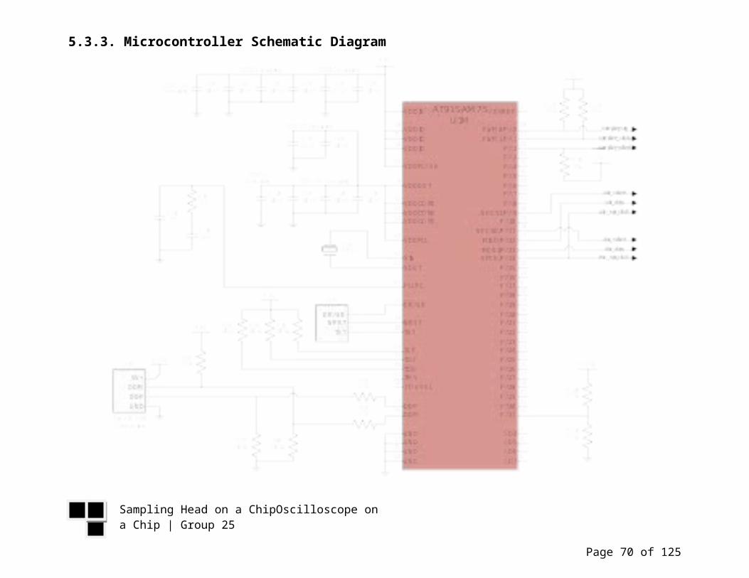
MOSFET ON Resistance
Figure 30: CMOS Transmission Gate
The MOSFET does not behave as a short in triode region, and has a resistance of few thousand ohms across its drain and source, which is also known as the ON resistance of a MOSFET. This ON resistance increases rapidly as the MOSFET moves into either cutoff or saturation. The large ON resistance creates two problems to our sampler: it decreases the input dynamic range and limits the input bandwidth. One way to expand the input range and to limit the ON resistance is to use a transmission gate, as shown in Figure 28. A PMOS transistor is connection in parallel with the NMOS so that the PMOS will start to conduct once the input voltage is raised beyond one threshold voltage below the clock ON, and will dominate the equivalent resistance across both transistors.
Charge Injection
Figure 31: NMOS Sampling Switch with “Dummy” MOSFET
The charge injection comes about as a result of the clock’s falling edge. The electrical field across the oxide layer between the gate and the substrate suddenly disappears, but the charges that are still were attracted toward the gate still reside in the inversion channel. These free charges would inject into the drain and the source of the MOSFET depending on the output impedances seen at both places. These charges create a nonlinearly voltage level shift across the hold capacitor, and distorts the output signal. The current solution calls for a dummy MOSFET that is placed after the sample-and-hold circuit, shown in Figure 29. With the drain and the source shorted together, this circuit does not modify the signal. Its gate is tied to the complement of the clock, so that when the sample-and-hold MOSFET experiences a falling edge, the dummy MOSFET will be turned on and drains the excess charges that are injected onto the capacitor.
Sampling Head on a ChipOscilloscope on a Chip | Group 25
Page 70 of 92
Clock Feed-throughClock feed-through is an effect caused by the parasitic capacitance of the MOSFET. The two major parasitic, the gate-source capacitance and the gate drain capacitance, are both connected to the gate, which is also the input for the sampling clock. The high frequency components inside the clock’s fast rising edge and falling edge makes the capacitors appear as a low resistance path, thus shorting the clock voltage with both the input and the output, and contributes to the overall distortion. One way to reduce the effect of clock feed-though is to minimize the transistor sizing. With a processing technology of 0.5um, clock feed-through will not be as nearly as significant as charge injection and large ON resistance.
Buffer Stage
Figure 32: Buffer Stage Schematic
The two sample-and-hold circuits are set up in master-slave configuration to act as an analog flip-flop. A buffer stage is added in the middle to separate the two hold capacitor from sharing charges, which reduces the input bandwidth. With a buffer stage in place, the hold capacitor at the second sample-and-hold circuit (slave) would be able to track the first hold capacitor with minimal delay. This buffer stage consists of a common-drain MOSFET (source follower) realized with both NMOS and PMOS transistors. Figure 30 shows the implementation for the source follower. The PMOS at the input level shift up by one threshold voltage, and the NMOS that follows provides a low-impedance output that boosts the current gain.
Sampling Head on a ChipOscilloscope on a Chip | Group 25
Page 71 of 92

6.3. Output Stage Unit Block Diagram (Level 2)
Figure 33: Output Stage Block Diagram
6.3.1. Output Stage Interface DefinitionThe sampler output and the amplified output have already been defined in Table 11. To avoid listing out the identical interface description, Table 21 only shows definitions that are specific to the Level 2 Output Stage block diagram.
Name Type Voltage Current Waveform/Frequency Notes
Filtered Output
InternalElectrical -
Analog
Max: 3.3 V (chip VDD)
Min: 0 V (ground)
Typ.: <1µA Periodic<1 MHz
This interface is nearly identical to the amplified output except that it has been passed through a single pole low pass filter with a cutoff frequency of 1 MHz. This way, all the higher frequency components that were the result of the sample-and-hold process are attenuated and will not be seen by the receiver, which is the off-chip ADC.
Table 21: Output Stage Interface Definition
6.3.2 Output Stage Unit Operation
The output stage consists of a 10MHz, single-stage, single-ended OPAMP realized using the same 0.5 micron processing technology as the sampling switch, and configured in a unity-gain feedback. Its main purpose is similar to the buffer stage inside the MOSFET sampling switch: to prevent the off-chip circuit from loading the on-chip sampler. The original design was implemented using several current mirrors with an overall gain of a hundred. However, because the squared relationship that exist between the large signal voltage and current, the voltage-to-current conversion process would produce excess distortion at the output.
Sampling Head on a ChipOscilloscope on a Chip | Group 25
Page 72 of 92

The second purpose of the output stage is the filtering of high frequency switching noise beyond 1MHz. Because the frequency of interest is the beat frequency between the input signal and the sampling clock, any components above the fixed 1MHz should be attenuated. Since the dominate pole lies on the output node of the OPAMP, the load capacitance would determine the exact the location of the cutoff frequency. For simulation purpose, the load capacitance is set at 20pF, which is corresponds to the input capacitance of the ADC. A too small of a load capacitance reduces the phase margin and introduces instability to the OPAMP, and a large load capacitance would severely limit the input bandwidth of the output stage. Even though replacing the current mirror with a single-stage OPAMP reduces the non-linearity at the output, one problem with the output stage is the DC scaling of the input. The common mode input and output range will limit the effective range of operation. An input voltage higher than the maximum allowed would push the MOSFET at the input into triode, and an input voltage less than the minimum allowed would push the tail MOSFET into triode. And the similar situation happens at the output.
6.3.3. Output Stage Unit Simulation The simulation for the output stage is also done in PSPICE, as with the system-level on-chip sampler simulation. The schematic for the output stage is shown in Figure 32. The simulation is set up as an AC sweep that scales in decade from 10Hz to 10GHz. As one can see, the response graph in Figure 33 shows that the -3dB frequency occurs at 1MHz, and the unity gain amplifier is stable up to 100MHz, which is a decade beyond our minimum requirement.
Figure 34: Output Stage Schematic
Sampling Head on a ChipOscilloscope on a Chip | Group 25
Page 73 of 92
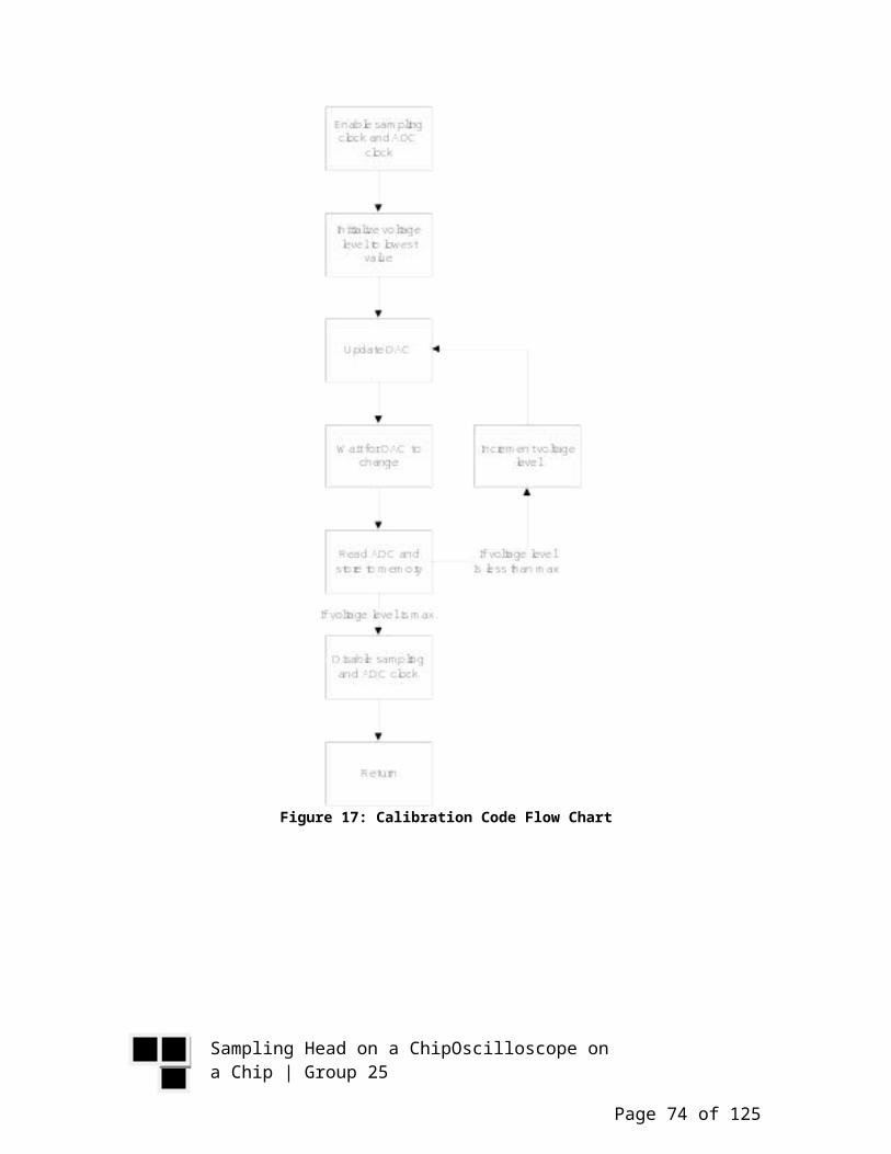
Figure 35: Output Stage Simulation Results (Bode Plot)
Sampling Head on a ChipOscilloscope on a Chip | Group 25
Page 74 of 92

7. Test Plan
7.1. Functional Test
Table 22: Functional Test Plan
Sampling Head on a ChipOscilloscope on a Chip | Group 25
Page 75 of 92

7.2. System Test
Table 23: System Test Plan Part 1
Sampling Head on a ChipOscilloscope on a Chip | Group 25
Page 76 of 92
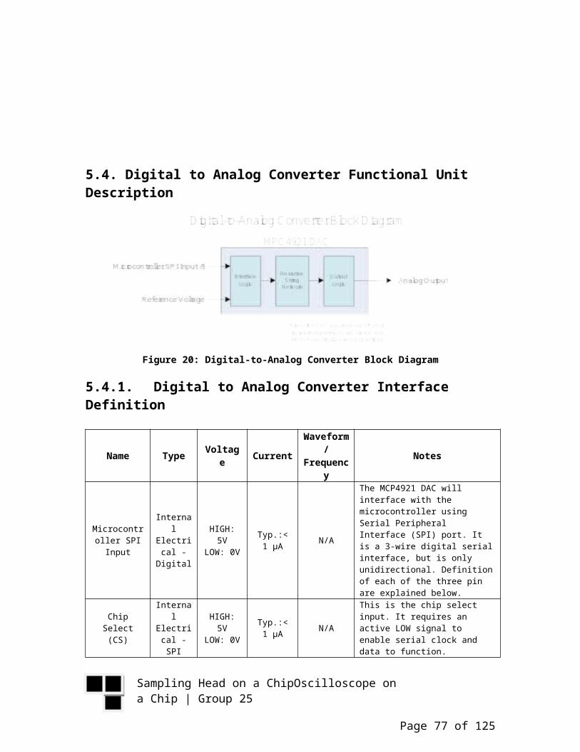
Table 24: System Test Plan Part
Sampling Head on a ChipOscilloscope on a Chip | Group 25
Page 77 of 92
7.3. Manufacturing Test
Table 25: Manufacturing Test Plan
7.4. Safety Test
Table 26: Safety Test Plan
7.5. Reliability Test
Table 27: Reliability Test Plan
Sampling Head on a ChipOscilloscope on a Chip | Group 25
Page 78 of 92

8. Bill of Materials and Suppliers
8.1. On-chip Sampler Parts List
Table 28: Sampler Parts List
Sampling Head on a ChipOscilloscope on a Chip | Group 25
Page 79 of 92
8.2. ADC Parts List
Table 29: ADC Parts List
Sampling Head on a ChipOscilloscope on a Chip | Group 25
Page 80 of 92
8.3. Microcontroller Parts List
Table 30: Microcontroller Parts List
Sampling Head on a ChipOscilloscope on a Chip | Group 25
Page 81 of 92

8.4. DAC Parts List
8.5. User Interface Parts ListThe user interface requires no parts other than a functional computer with at least one available USB port and Visual Studio installed.
Sampling Head on a ChipOscilloscope on a Chip | Group 25
Page 82 of 92

8.6 Voltage Regulator Parts List
Table 31: Voltage Regulator Parts List
Sampling Head on a ChipOscilloscope on a Chip | Group 25
Page 83 of 92
Appendix A: References
[1] R. Ho, B. Amrutur, K. Mai, B. Wilburn, T. Mori, and M. Horowitz. “Applications of on-chip samplers for test and measurement of integrated circuits.” Symposium on VLSI Circuits Digest of Technical Papers, pp. 138-139, 1998.
[2] Frankie Liu, Ron Ho, et. al. “On-chip samplers for test and debug of asynchronous circuits,” 13th IEEE International Symposium on Asynchronous Circuits and Systems. pp. 153-162. 2007.
[3] Richard II Stallup, “Probing Transistors at the Contact Level in Integrated Circuits,” 2004, http://www.keithley.com.
[4] Tektronics, “Tektronics Oscilloscope Selection Chart,” no post date given, www.tek.com/products/oscilloscopes/selection_chart.html.
[5] Teradyne, “Teradyne - Semiconductor Test,” no post date given, http://www.teradyne.com/std.
[6] David F. Hoeschele Jr, Analog-to-Digital/Digital-to-Analog Conversion Techniques. New York: John Wiley & Sons, Inc., 1968, pp. 7-10.
[7] Bernard Loriferne, Analog-Digital and Digital-Analog Conversion. Philadelphia: Hayden & Son Ltd., 1982, pp. 77-102.
[8] MCT Paul & Scherer, “SPI – Serial Peripheral Interface,” September 2006, http://www.mct.net/faq/spi.html.
[9] “Universal Asynchronous Receiver/Transmitter,” no post date given, http://en.wikipedia.org/wiki/UART.
[10] Intel Corporation, ”Universal Serial Bus (USB),” no post date given, http://www.intel.com/technology/usb.
[11] Farag F. A., M. C. Schneider and C. Galup-Montoro, “A Fully Balanced Programmable Sample-Hold Amplifier for Low-Voltage Applications,” May 2000, http://ieeexplore.ieee.org/iel5/6910/18588/00856092.pdf.
[12] Liang Dai and Ramesh Harjani, “CMOS Switched-OP-Amp Sample-and-Hold Circuit,” December 1999, http://www.ics.ee.nctu.edu.tw/~jtwu/courses.
Sampling Head on a ChipOscilloscope on a Chip | Group 25
Page 84 of 92
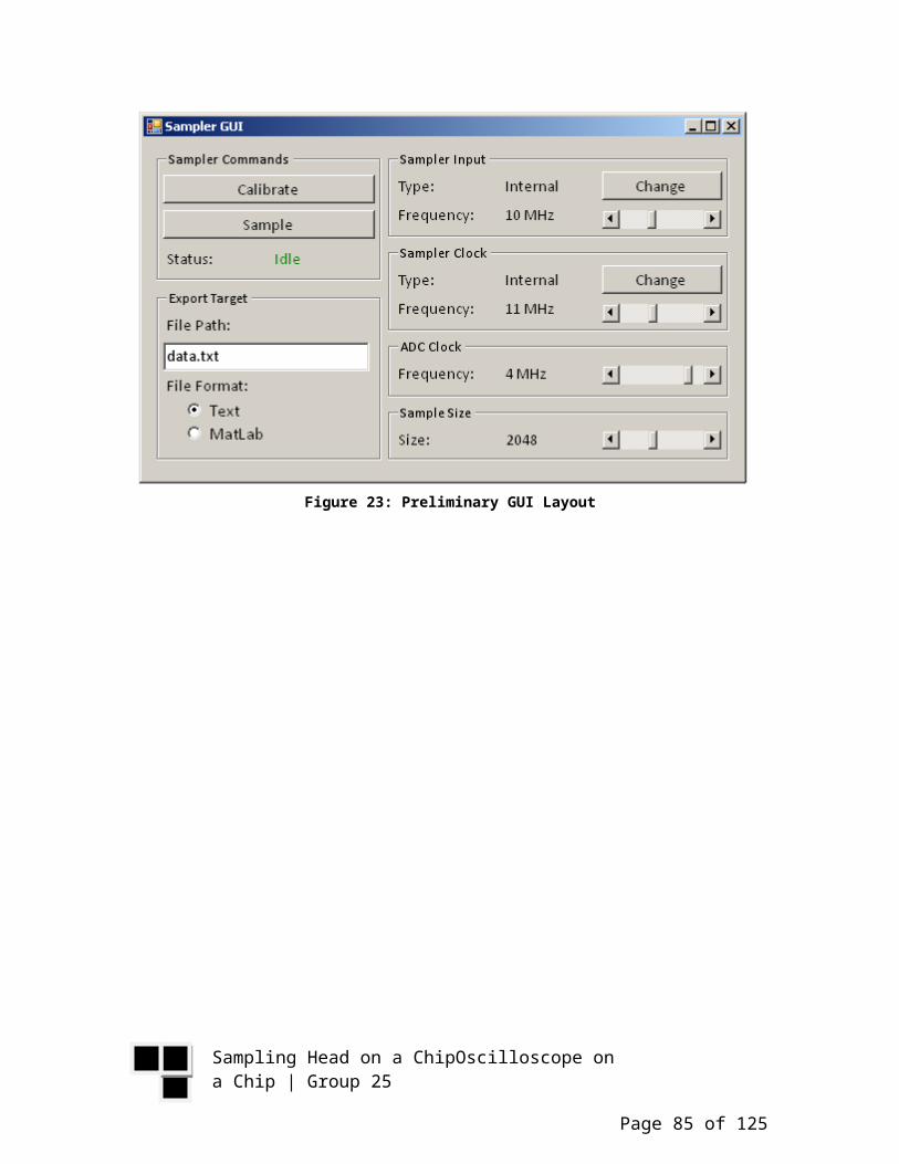
[13] Ming-Jer Chen, Yen-Bin Gu, Jen-Yin Huang, Wei-Chen Shen, Terry Wu, and Po-Chin Hsu, “A Compact High-Speed Miller Capacitance Based Sample-and-Hold,” March 1996, http://ieeexplore.ieee.org.
[14] Razavi, Bhezad, “A 200-MHZ 15mW BiCMOS Sample-and-Hold Amplifier with 3V Supply,” August 1995, http://www.ee.ucla.edu/~brweb/papers/Journals.
[15] National Semiconductor, “LM1084 5A Low Dropout Positive Regulators,” August 2002, http://www.jameco.com/Jameco/Products/ProdDS/299735NSC.pdf.
[16] National Semiconductor, “LM1117/LM1117 800mA Low-Dropout Linear Regulator,” October 2002, http://www.jameco.com/Jameco/Products/ProdDS/242114NAT.pdf.
[17] Linear Technology “800mA Low Dropout Positive Regulators Adjustable and Fixed 2.85V, 3.3V, 5V,” no post date given, http://www.jameco.com/Jameco/Products/ProdDS/1730574.pdf.
[18] Howe, Denis. “Free On-Line Dictionary of Computing,” no post date given, http://foldoc.org.
[19] P. Larsson and C. Svensson, “Measuring high-bandwidth signals in CMOS circuits,” Electronic Letters, vol. 29, pp. 1761-2, September 1992.
[20] National Semiconductor Corporation, ABCs of ADCs Application Note, 2006.
[21] G. W. Roberts, “Improving the testability of mixed-signal of integrated circuit” in IEEE Custom Integrated Circuits Conference, May 1997, pp. 214-221.
[22] Atmel Corporation, "AT91RM9200," September 2006, http://www.atmel.com/dyn/products/.
[23] Atmel Corporation, “AT91SAM7S Series Preliminary,” November 2006. http://www.atmel.com/dyn/products/.
[24] Atmel Corporation, "AT90USB1286, AT90USB1287, AT90USB646, AT90USB647 Preliminary," June 2007, http://www.atmel.com/dyn/products/.
[25] Leroy Davis, "Operational Temperature Ranges," January 2007, http://www.interfacebus.com/Logic_Prefix_Temp_Range.html.
Sampling Head on a ChipOscilloscope on a Chip | Group 25
Page 85 of 92
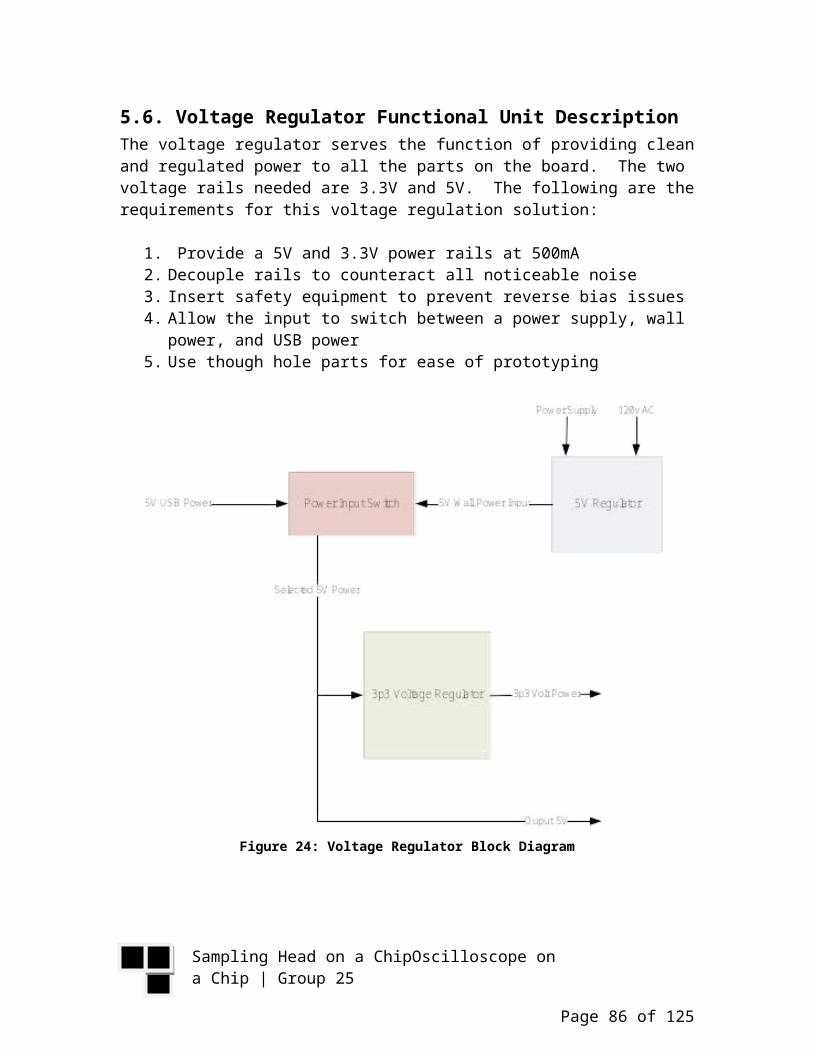
Appendix B: Naming Conventions and Glossary
Analog Refers to data that can take on an infinite set of values
ADC Analog to Digital Converter – A device that converts analog signals that contains a continuous range of values to a digital signal represented in discrete a binary number. See Data Converter
ATE Automatic Test Equipment – Devices used to probe and validate silicon wafers, PCB and IC
Bond Pads Metal pads on a silicon chip used as contacts for external probes.
Capacitance A measurement of amount of charge capable of being stored in a capacitor.
CONV Conversion Start – This is an input to the ADC showing when to start a conversion for the display of a value word.
CMOS Complementary Metal Oxide Semiconductor – a silicon technology widely used for Integrated Circuits
DAC Digital to Analog Converter – A device that converts analog signals that contains a continuous range of values to a digital signal represented in discrete a binary number. See Data Converter
Data Converter A device used to translate analog signals to digital or digital signals to the analog domain. See ADC, DAC
Demultiplexer A device that allows the connection of an output to one particular input at a time based on control signals.
Differential Signaling A type of signaling where two inverted inputs are taken and subtracted to subdue noise and preserve signal quality.
Digital Refers to data in the form of 1’s and 0’s, a discrete array of values
ESR Equivalent Series Resistance – The resistance of a lead of a capacitor, which should be minimized in capacitors used for stability of voltage regulators.
Sampling Head on a ChipOscilloscope on a Chip | Group 25
Page 86 of 92

FPGA Field Programmable Gate Array – A device that contains digital hardware that can be reconfigured through programming.
JTAG Joint Test Action Group -- Protocol used to communicate with boundary scan, which is on-chip debug circuitry for digital ICs
IC Integrated Circuit – An electronic circuit built into one piece of silicon
LCD Liquid Crystal Display – A specialized display controlled by an IC
Microcontroller A programmable logic device used to manipulate Input and output signals
MATLAB A commonly used engineering and mathematical software tool that can simulate filtering designs well
MOSFET Metal Oxide Semiconductor Field Effect Transistor – Transistor we will use in our circuit designs
MTBF Mean Time Between Failures – The average amount of time that passes before another failure is detected
MTTR Mean Time To Repair – The average amount of time taken to recover from a failure
Multiplexer A device that allows the connection of an input to one particular output at a time based on control signals.
Node A region in a circuit where there is no change in potential
PCB Printed Circuit Board – The board on which parts are physically placed
Probe A deice used to measure a value of a node in a circuit
Oscilloscope A device used to measure signaling characteristics
OP‐AMP Operational Amplifier, a circuit device used as a gain stage or filter
Sampling Head The portion of the oscilloscope on a chip circuit that will convert the input into discrete samples that can then be measured
Sampling Head on a ChipOscilloscope on a Chip | Group 25
Page 87 of 92

SCK Serial Clock – An input pin of the ADC where the clock is fed from the microcontroller
SDO Serial Data Out – The digital output pin of the ADC which feeds a signal to the microcontroller
SHDN Shutdown -- This refers to the output power down control for the Digital to analog converter
S/H Sample and Hold – Technique for non intrusively probing signal‐
SNR Signal to Noise Ratio – The ratio of signal power to noise power
SPI Serial Peripheral Bus – A common serial bus standard for embedded systems and computers
SUT System Under Test – The transistor devices that are being tested
UART Universal Asynchronous Receiver/Transmitter -- The protocol used on the serial port for computers.
USB Universal Serial Bus – A digital bus commonly used for computer peripherals.
VLSI Very Large Scale Integration – The technology of creating circuits with thousands of transistors in a small space.
Sampling Head on a ChipOscilloscope on a Chip | Group 25
Page 88 of 92
Appendix C: Media Release
This is the media release developed to spark interest in the on-chip sampler project:
“To most people electricity is a mysterious study dominated by tiny boards with electric signals running though a plethora of even tinier parts. It’s nearly impossible to determine the shape of the signals running though integrated circuit chips (those little black boxes on a circuit board). To solve this problem, our group has devised a method of embedding a sampler within an integrated circuit chip that will read signals on that chip and display them on a computer screen, effectively opening the hidden world of circuits to the average user.”
Sampling Head on a ChipOscilloscope on a Chip | Group 25
Page 89 of 92
Appendix D: Revisions Based on Preliminary Design Specification Comments
1. In Section 2, Paragraph 6, it was noted that we used the phrase “The on-chip sampler samples the node under test…” The flow of the paper was disrupted by the use of “sampler” followed directly with “samples.” This text was changed in the final report to “The on-chip sampler detects the node voltage under test…” While requiring slightly more though, this phrase doesn’t detract from the flow of the paper.
2. In Section 2.1, Paragraph 1, it was noted that the term “oscilloscope on a chip” was unhyphenated. That instance has now been hyphenated and all other instances have been changed to on-chip oscilloscope for consistency.
3. In Section 2.1, Paragraph 5, it was noted that the sentence “But even though the on-chip oscilloscope offers better performance for sensing analog signals, it would always be integrated into a larger VLSI system” started with a contraction and included an acronym not defined in the glossary. The term VLSI has been added to the glossary, and the sentence has been revised for grammatical consistency.
4. In Section 2.3.1, the receiver noted that the second requirement “Converts analog signals to digital data transferable to standard PC” was not specific enough. Our design however, calls for a software interface to analyze the data, but no constraints are placed on that interface. Assuming this to be the meaning of the reviewers comments, our group decided that this would not be changed.The second comment about requirement number three was one the group felt needed to be addressed. Thus is has been changed from “Includes a calibration mode for the detection of inaccurate data” to “Includes a calibration mode for the creation of a transfer function lookup table.” The intention of the calibration mode is to get rid of inaccurate data, but the range of inaccuracies was not meant to be defined. Rather, the creation of a look-up table to counteract possible distortion was the intention of the calibration mode.
5. Passive sentences are prolific in our writing and measures have been taken to eliminate all that make sense. However, some seem necessary such to match with the logic flow of the paper. The passive sentence in question “A calibration mode is implemented by injecting a known direct current (DC) bias to the sampler and checking the sampler output accordingly” was not deemed to be too distracting to the reader. Also a better solution for this sentence could not be found so it was left as it was.
Sampling Head on a ChipOscilloscope on a Chip | Group 25
Page 90 of 92
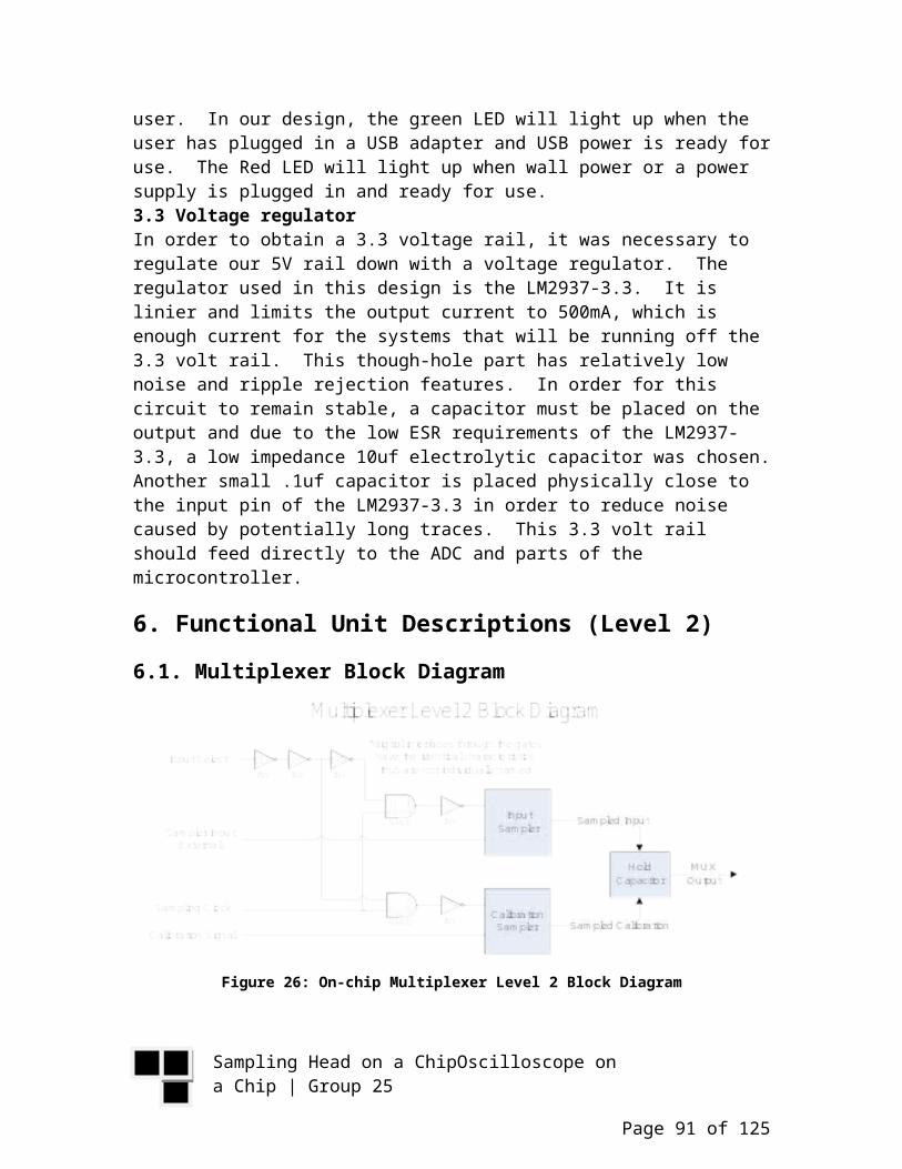
6. Our paper was found to contain a few limited tense changes. These have been removed and changed to the present tense.
7. The phrase “which interfaces the end user” can be misconstrued and sounds odd. This was changed to “which provides and interface for the end user” in order to retain the logical flow of the paper.
8. Setup and hold times are not required for most of the signals due to their analog or non-critical nature. In the comments for signals, set-up and hold times are discussed if it is important. However, due to the limited setup and hold requirements, a new column for the table was not made for this parameter.
Sampling Head on a ChipOscilloscope on a Chip | Group 25
Page 91 of 92
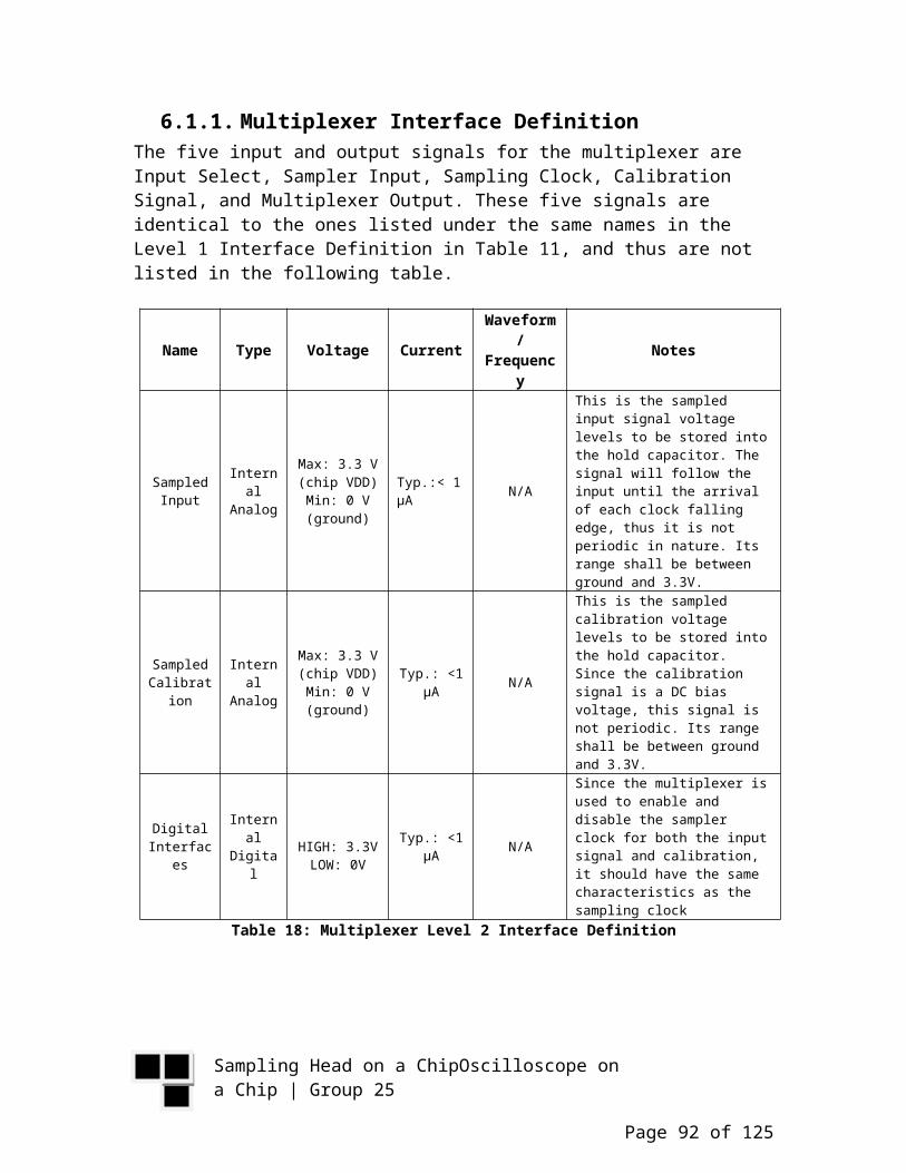
Appendix E: Other Select Revisions from Preliminary Design Specification
1. In Section 2, Paragraph 1, the introductory sentence was “The goal of this project is to design, prototype and test ….” This line was changed in the final paper to “This project presents a design to prototype and test” in order to better clarify the purpose of the paper and write in a way that is consistent with other industry papers.
2. In Section 2, Paragraph 2, the term “bond pads” was defined in the glossary.
3. In Section 2, Paragraph 3, the sentence “As the size of the ICs decreases and the complexity and bandwidth of the devices increases, testing of sensitive nodes becomes increasingly difficult” was flagged as being questionable. It was changed to a more grammatically correct form “As the size of ICs decrease and the complexity and bandwidth of the devices increase, the testing of sensitive nodes becomes increasingly difficult.”
4. In section 2, Paragraph 3, the sentence “The three major limitations were associated with the conventional approach of probing ICs using an external device:” was replaced with “Three major limitations were associated with the conventional approach of probing ICs using an external device:” in order to facilitate flow.
5. In section 2, Paragraph 5, the sentence “This project strives to overcome these limitations…” was changed to “This project overcomes these limitations” in order to increase clarity.
6. In section 2, Paragraph 6, the sentence “The digital data, using either parallel or serial means, will be processed with a microcontroller before they are compatible with PC” was changed to “The digital data lines will be processed with a microcontroller using either parallel or serial means before they are compatible with a PC” in order to minimize the use of passive sentences.
Sampling Head on a ChipOscilloscope on a Chip | Group 25
Page 92 of 92


![Guerber - Reynard the Fox - bestiary.cabestiary.ca/etexts/guerber1896/guerber - reynard the fox.pdf · 1 REYNARD THE FOX [35] Among primitive races, as with children, animal stories](https://img.pdfslide.us/doc/110x75/5b2944d67f8b9af9128b46b1/guerber-reynard-the-fox-reynard-the-foxpdf-1-reynard-the-fox-35-among.jpg)