Embed Size (px)
Citation preview
March 2011 Doc ID 15287 Rev 5 1/24
AN2867Application noteOscillator design guide for ST microcontrollers
IntroductionMost designers are familiar with oscillators (Pierce-Gate topology), but few really understand how they operate, let alone how to properly design an oscillator. In practice, most designers do not even really pay attention to the oscillator design until they realize the oscillator does not operate properly (usually when it is already being produced). This should not happen. Many systems or projects are delayed in their deployment because of a crystal not working as intended. The oscillator should receive its proper amount of attention during the design phase, well before the manufacturing phase. The designer would then avoid the nightmare scenario of products being returned.
This application note introduces the Pierce oscillator basics and provides some guidelines for a good oscillator design. It also shows how to determine the different external components and provides guidelines for a good PCB for the oscillator.This document finally contains an easy guideline to select suitable crystals and external components, and it lists some recommended crystals (HSE and LSE) for STM32™ and STM8A/S microcontrollers in order to quick start development.
www.st.com

Contents AN2867
2/24 Doc ID 15287 Rev 5
Contents
1 Quartz crystal properties and model . . . . . . . . . . . . . . . . . . . . . . . . . . . . 6
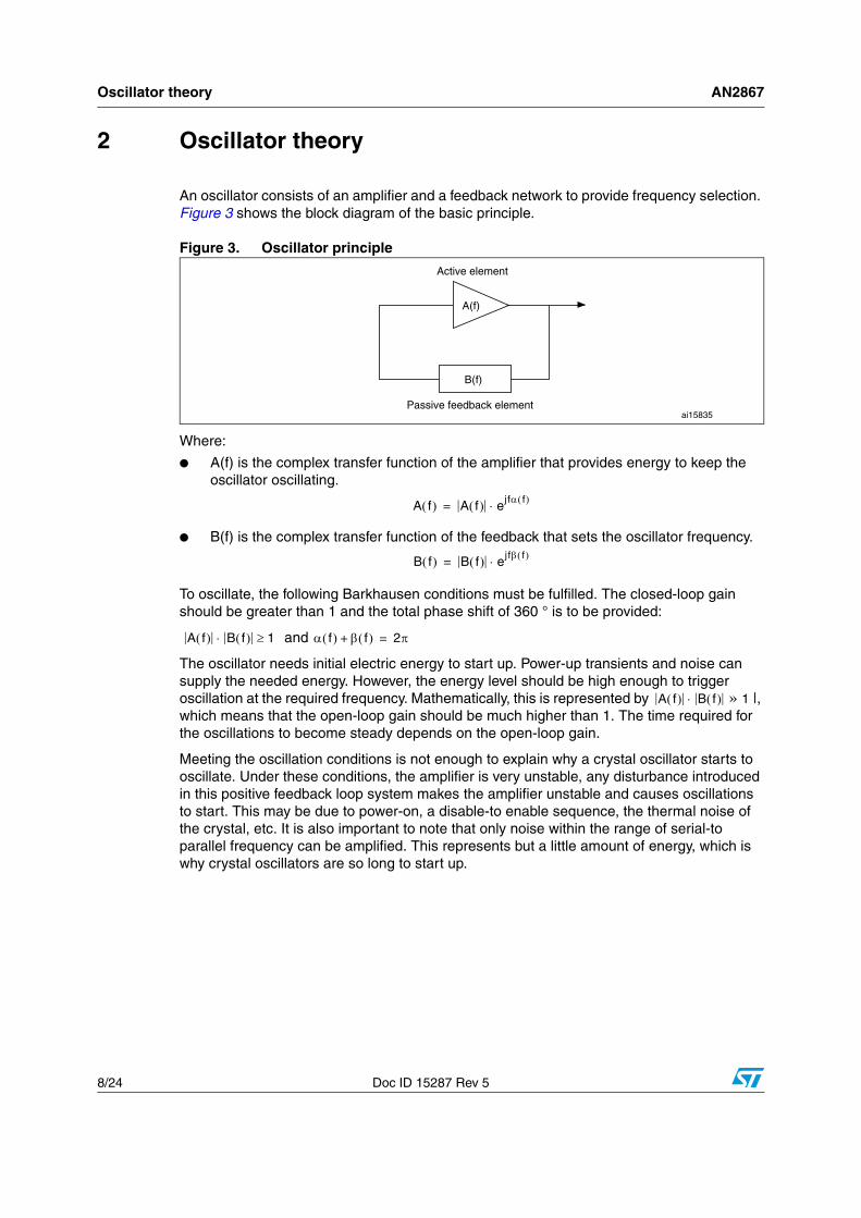
2 Oscillator theory . . . . . . . . . . . . . . . . . . . . . . . . . . . . . . . . . . . . . . . . . . . . 8
3 Pierce oscillator . . . . . . . . . . . . . . . . . . . . . . . . . . . . . . . . . . . . . . . . . . . . . 9
4 Pierce oscillator design . . . . . . . . . . . . . . . . . . . . . . . . . . . . . . . . . . . . . 10
4.1 Feedback resistor RF . . . . . . . . . . . . . . . . . . . . . . . . . . . . . . . . . . . . . . . . 10
4.2 Load capacitor CL . . . . . . . . . . . . . . . . . . . . . . . . . . . . . . . . . . . . . . . . . . . . . . . . . . . . . . 11
4.3 Gain margin of the oscillator . . . . . . . . . . . . . . . . . . . . . . . . . . . . . . . . . . . 11
4.4 Drive level DL and external resistor RExt calculation . . . . . . . . . . . . . . . . 12
4.4.1 Calculating drive level DL . . . . . . . . . . . . . . . . . . . . . . . . . . . . . . . . . . . 12
4.4.2 Another drive level measurement method . . . . . . . . . . . . . . . . . . . . . . . 13
4.4.3 Calculating external resistor RExt . . . . . . . . . . . . . . . . . . . . . . . . . . . . . 13
4.5 Startup time . . . . . . . . . . . . . . . . . . . . . . . . . . . . . . . . . . . . . . . . . . . . . . . 14
4.6 Crystal pullability . . . . . . . . . . . . . . . . . . . . . . . . . . . . . . . . . . . . . . . . . . . 14
5 Easy guideline for the selection of suitable crystaland external components . . . . . . . . . . . . . . . . . . . . . . . . . . . . . . . . . . . . 15
6 Some recommended crystals for STM32™ microcontrollers . . . . . . . 16
6.1 HSE part . . . . . . . . . . . . . . . . . . . . . . . . . . . . . . . . . . . . . . . . . . . . . . . . . . 16
6.1.1 Part numbers of recommended 8 MHz crystals . . . . . . . . . . . . . . . . . . . 16
6.1.2 Part numbers of recommended ceramic resonators . . . . . . . . . . . . . . . 17
6.1.3 Part numbers of recommended 25 MHz crystals(Ethernet applications) . . . . . . . . . . . . . . . . . . . . . . . . . . . . . . . . . . . . . . 17
6.1.4 Part numbers of recommended 14.7456 MHz crystals (audioapplications) . . . . . . . . . . . . . . . . . . . . . . . . . . . . . . . . . . . . . . . . . . . . . . 18
6.2 LSE part . . . . . . . . . . . . . . . . . . . . . . . . . . . . . . . . . . . . . . . . . . . . . . . . . . 19
7 Some recommended crystals for STM8A/S microcontrollers . . . . . . . 20
7.1 Part numbers of recommended crystal oscillators . . . . . . . . . . . . . . . . . . 20
7.2 Part numbers of recommended ceramic resonators . . . . . . . . . . . . . . . . 20
8 Some PCB hints . . . . . . . . . . . . . . . . . . . . . . . . . . . . . . . . . . . . . . . . . . . 21

AN2867 Contents
Doc ID 15287 Rev 5 3/24
9 Conclusion . . . . . . . . . . . . . . . . . . . . . . . . . . . . . . . . . . . . . . . . . . . . . . . . 22
10 Revision history . . . . . . . . . . . . . . . . . . . . . . . . . . . . . . . . . . . . . . . . . . . 23

List of tables AN2867
4/24 Doc ID 15287 Rev 5
List of tables
Table 1. Example of equivalent circuit parameters . . . . . . . . . . . . . . . . . . . . . . . . . . . . . . . . . . . . . . . 7Table 2. Typical feedback resistor values for given frequencies . . . . . . . . . . . . . . . . . . . . . . . . . . . 10Table 3. EPSON® . . . . . . . . . . . . . . . . . . . . . . . . . . . . . . . . . . . . . . . . . . . . . . . . . . . . . . . . . . . . . . . . . . . . . . . . . . . . . . . 16
Table 4. HOSONIC ELECTRONIC. . . . . . . . . . . . . . . . . . . . . . . . . . . . . . . . . . . . . . . . . . . . . . . . . . 16Table 5. CTS® . . . . . . . . . . . . . . . . . . . . . . . . . . . . . . . . . . . . . . . . . . . . . . . . . . . . . . . . . . . . . . . . . . . . . . . . . . . . . . . . . . . 16
Table 6. FOXElectronics®. . . . . . . . . . . . . . . . . . . . . . . . . . . . . . . . . . . . . . . . . . . . . . . . . . . . . . . . . . . . . . . . . . . . . . . . 16
Table 7. Recommendable conditions (for consumer) . . . . . . . . . . . . . . . . . . . . . . . . . . . . . . . . . . . . 17Table 8. HOSONIC ELECTRONIC. . . . . . . . . . . . . . . . . . . . . . . . . . . . . . . . . . . . . . . . . . . . . . . . . . 17Table 9. FOXElectronics®. . . . . . . . . . . . . . . . . . . . . . . . . . . . . . . . . . . . . . . . . . . . . . . . . . . . . . . . . . . . . . . . . . . . . . . . 17
Table 10. CTS® . . . . . . . . . . . . . . . . . . . . . . . . . . . . . . . . . . . . . . . . . . . . . . . . . . . . . . . . . . . . . . . . . . . . . . . . . . . . . . . . . . . 17
Table 11. FOXElectronics®. . . . . . . . . . . . . . . . . . . . . . . . . . . . . . . . . . . . . . . . . . . . . . . . . . . . . . . . . . . . . . . . . . . . . . . . 18
Table 12. ABRACON™ . . . . . . . . . . . . . . . . . . . . . . . . . . . . . . . . . . . . . . . . . . . . . . . . . . . . . . . . . . . 18Table 13. Recommendable crystals . . . . . . . . . . . . . . . . . . . . . . . . . . . . . . . . . . . . . . . . . . . . . . . . . . 19Table 14. KYOCERA . . . . . . . . . . . . . . . . . . . . . . . . . . . . . . . . . . . . . . . . . . . . . . . . . . . . . . . . . . . . . 20Table 15. Recommendable conditions (for consumer) . . . . . . . . . . . . . . . . . . . . . . . . . . . . . . . . . . . . 20Table 16. Recommendable conditions (for CAN-BUS). . . . . . . . . . . . . . . . . . . . . . . . . . . . . . . . . . . . 20Table 17. Document revision history . . . . . . . . . . . . . . . . . . . . . . . . . . . . . . . . . . . . . . . . . . . . . . . . . 23

AN2867 List of figures
Doc ID 15287 Rev 5 5/24
List of figures
Figure 1. Quartz crystal model . . . . . . . . . . . . . . . . . . . . . . . . . . . . . . . . . . . . . . . . . . . . . . . . . . . . . . . 6Figure 2. Impedance representation in the frequency domain. . . . . . . . . . . . . . . . . . . . . . . . . . . . . . . 6Figure 3. Oscillator principle . . . . . . . . . . . . . . . . . . . . . . . . . . . . . . . . . . . . . . . . . . . . . . . . . . . . . . . . 8Figure 4. Pierce oscillator circuitry . . . . . . . . . . . . . . . . . . . . . . . . . . . . . . . . . . . . . . . . . . . . . . . . . . . . 9Figure 5. Inverter transfer function. . . . . . . . . . . . . . . . . . . . . . . . . . . . . . . . . . . . . . . . . . . . . . . . . . . 10Figure 6. Current drive measurement with a current probe . . . . . . . . . . . . . . . . . . . . . . . . . . . . . . . . 12Figure 7. Recommended layout for an oscillator circuit . . . . . . . . . . . . . . . . . . . . . . . . . . . . . . . . . . . 21

Quartz crystal properties and model AN2867
6/24 Doc ID 15287 Rev 5
1 Quartz crystal properties and model
A quartz crystal is a piezoelectric device transforming electric energy to mechanical energy and vice versa. The transformation occurs at the resonant frequency. The quartz crystal can be modeled as follows:
Figure 1. Quartz crystal model
C0: represents the shunt capacitance resulting from the capacitor formed by the electrodes
Lm: (motional inductance) represents the vibrating mass of the crystal
Cm: (motional capacitance) represents the elasticity of the crystal
Rm: (motional resistance) represents the circuit losses
The impedance of the crystal is given by the following equation (assuming that Rm is negligible):
(1)
Figure 2 represents the impedance in the frequency domain.
Figure 2. Impedance representation in the frequency domain
Fs is the series resonant frequency when the impedance Z = 0. Its expression can be deduced from equation (1) as follows:
(2)
Q
C0
Rm CmLm
ai15833
Z jw----
w2LmCm 1–
C0 Cm+ w2LmCmC0–----------------------------------------------------------------=
Fs Fa
Impedance
Inductive behavior:the quartz oscillates
Area of parallelresonance: Fp
Capacitive behavior:no oscillation
Phase (deg)
Frequency
Frequency
+90
–90
ai15834
Fs1
2 LmCm
---------------------------=

AN2867 Quartz crystal properties and model
Doc ID 15287 Rev 5 7/24
Fa is the anti-resonant frequency when impedance Z tends to infinity. Using equation (1), it is expressed as follows:
(3)
The region delimited by Fs and Fa is usually called the area of parallel resonance (shaded area in Figure 2). In this region, the crystal operates in parallel resonance and behaves as an inductance that adds an additional phase equal to 180 ° in the loop. Its frequency Fp (or FL: load frequency) has the following expression:
(4)
From equation (4), it appears that the oscillation frequency of the crystal can be tuned by varying the load capacitor CL. This is why in their datasheets, crystal manufacturers indicate the exact CL required to make the crystal oscillate at the nominal frequency.
Table 1 gives an example of equivalent crystal circuit component values to have a nominal frequency of 8 MHz.
Using equations (2), (3) and (4) we can determine Fs, Fa and Fp of this crystal:
and .
If the load capacitance CL at the crystal electrodes is equal to 10 pF, the crystal will oscillate at the following frequency: .
To have an oscillation frequency of exactly 8 MHz, CL should be equal to 4.02 pF.
Table 1. Example of equivalent circuit parameters
Equivalent component Value
Rm 8
Lm 14.7 mH
Cm 0.027 pF
C0 5.57 pF
Fa Fs 1Cm
C0--------+=
Fp Fs 1Cm
2 C0 CL+ -----------------------------+
=
Fs 7988768 Hz= Fa 8008102 Hz=
Fp 7995695 Hz=
Oscillator theory AN2867
8/24 Doc ID 15287 Rev 5
2 Oscillator theory
An oscillator consists of an amplifier and a feedback network to provide frequency selection. Figure 3 shows the block diagram of the basic principle.
Figure 3. Oscillator principle
Where:
● A(f) is the complex transfer function of the amplifier that provides energy to keep the oscillator oscillating.
● B(f) is the complex transfer function of the feedback that sets the oscillator frequency.
To oscillate, the following Barkhausen conditions must be fulfilled. The closed-loop gain should be greater than 1 and the total phase shift of 360 ° is to be provided:
and
The oscillator needs initial electric energy to start up. Power-up transients and noise can supply the needed energy. However, the energy level should be high enough to trigger oscillation at the required frequency. Mathematically, this is represented by |, which means that the open-loop gain should be much higher than 1. The time required for the oscillations to become steady depends on the open-loop gain.
Meeting the oscillation conditions is not enough to explain why a crystal oscillator starts to oscillate. Under these conditions, the amplifier is very unstable, any disturbance introduced in this positive feedback loop system makes the amplifier unstable and causes oscillations to start. This may be due to power-on, a disable-to enable sequence, the thermal noise of the crystal, etc. It is also important to note that only noise within the range of serial-to parallel frequency can be amplified. This represents but a little amount of energy, which is why crystal oscillators are so long to start up.
Passive feedback element
A(f)
Active element
B(f)
ai15835
A f A f ejf f =
B f B f ejf f =
A f B f 1 f f + 2=
A f B f 1»

AN2867 Pierce oscillator
Doc ID 15287 Rev 5 9/24
3 Pierce oscillator
Pierce oscillators are commonly used in applications because of their low consumption, low cost and stability.
Figure 4. Pierce oscillator circuitry
Inv: the internal inverter that works as an amplifier
Q: crystal quartz or a ceramic resonator
RF: internal feedback resistor
RExt: external resistor to limit the inverter output current
CL1 and CL2: are the two external load capacitors
Cs: stray capacitance is the addition of the MCU pin capacitance (OSC_IN and OSC_OUT) and the PCB capacitance: it is a parasitical capacitance.
RExt
RF
Q
CL1 CL2
Microcontroller
Inv
Cs
ai15836
OSC_OUTOSC_IN
Pierce oscillator design AN2867
10/24 Doc ID 15287 Rev 5
4 Pierce oscillator design
This section describes the different parameters and how to determine their values in order to be more conversant with the Pierce oscillator design.
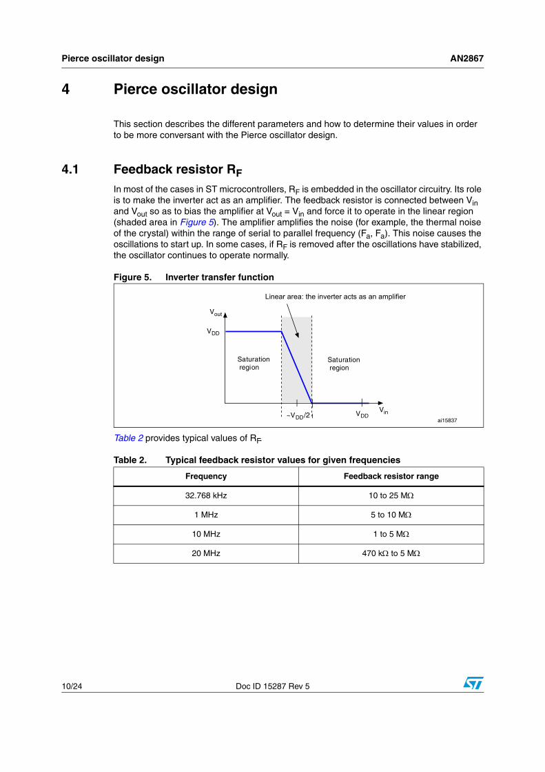
4.1 Feedback resistor RF
In most of the cases in ST microcontrollers, RF is embedded in the oscillator circuitry. Its role is to make the inverter act as an amplifier. The feedback resistor is connected between Vin and Vout so as to bias the amplifier at Vout = Vin and force it to operate in the linear region (shaded area in Figure 5). The amplifier amplifies the noise (for example, the thermal noise of the crystal) within the range of serial to parallel frequency (Fa, Fa). This noise causes the oscillations to start up. In some cases, if RF is removed after the oscillations have stabilized, the oscillator continues to operate normally.
Figure 5. Inverter transfer function
Table 2 provides typical values of RF.
Table 2. Typical feedback resistor values for given frequencies
Frequency Feedback resistor range
32.768 kHz 10 to 25 M
1 MHz 5 to 10 M
10 MHz 1 to 5 M
20 MHz 470 k to 5 M
~VDD/2 VDD
VDD
Linear area: the inverter acts as an amplifier
Saturation region
Saturation region
Vout
Vin
ai15837

AN2867 Pierce oscillator design
Doc ID 15287 Rev 5 11/24
4.2 Load capacitor CL
The load capacitance is the terminal capacitance of the circuit connected to the crystal oscillator. This value is determined by the external capacitors CL1 and CL2 and the stray capacitance of the printed circuit board and connections (Cs). The CL value is specified by the crystal manufacturer. Mainly, for the frequency to be accurate, the oscillator circuit has to show the same load capacitance to the crystal as the one the crystal was adjusted for. Frequency stability mainly requires that the load capacitance be constant. The external capacitors CL1 and CL2 are used to tune the desired value of CL to reach the value specified by the crystal manufacturer.
The following equation gives the expression of CL:
Example of CL1 and CL2 calculation:
For example if the CL value of the crystal is equal to 15 pF and, assuming that Cs = 5 pF, then:
. That is: .
4.3 Gain margin of the oscillatorThe gain margin is the key parameter that determines whether the oscillator will start up or not. It has the following expression:
, where:
● gm is the transconductance of the inverter (in mA/V for the high-frequency part or in µA/V for the low-frequency part: 32 kHz).
● gmcrit (gm critical) depends on the crystal parameters.
Assuming that CL1 = CL2, and assuming that the crystal sees the same CL on its pads as the value given by the crystal manufacturer, gmcrit is expressed as follows:
, where ESR = equivalent series resistor
According to the Eric Vittoz theory: the impedance of the motional RLC equivalent circuit of a crystal is compensated by the impedance of the amplifier and the two external capacitances.
To satisfy this theory, the inverter transconductance (gm) must have a value gm > gmcrit. In this case, the oscillation condition is reached. A gain margin of 5 can be considered as a minimum to ensure an efficient startup of oscillations.
For example, to design the oscillator part of a microcontroller that has a gm value equal to 25 mA/V, we choose a quartz crystal (from Fox) that has the following characteristics: frequency = 8 MHz, C0 = 7 pF, CL = 10 pF, ESR = 80 .. Will this crystal oscillate with this microcontroller?
Let us calculate gmcrit:
CLCL1 CL2CL1 CL2+-------------------------- Cs+=
CL Cs–CL1 CL2CL1 CL2+-------------------------- 10 pF== CL1 CL2= 20 pF=
gainm inarggm
gmcrit---------------=
gmcrit 4 ESR 2F 2 C0 CL+ 2=
gmcrit 4 80 2 8 610 2
7 12–10 10 12–10+ 2
0.23 mA V==
Pierce oscillator design AN2867
12/24 Doc ID 15287 Rev 5
Calculating the gain margin gives:
The gain margin is very sufficient to start the oscillation and the “gain margin greater than 5” condition is reached. The crystal will oscillate normally.
If an insufficient gain margin is found (gain margin < 5) the oscillation condition is not reached and the crystal will not start up. You should then try to select a crystal with a lower ESR or/and with a lower CL.
4.4 Drive level DL and external resistor RExt calculationThe drive level and external resistor value are closely related. They will therefore be addressed in the same section.
4.4.1 Calculating drive level DL
The drive level is the power dissipated in the crystal. It has to be limited otherwise the quartz crystal can fail due to excessive mechanical vibration. The maximum drive level is specified by the crystal manufacturer, usually in mW. Exceeding this maximum value may lead to the crystal being damaged.
The drive level is given by the following formula: , where:
● ESR is the equivalent series resistor (specified by the crystal manufacturer):
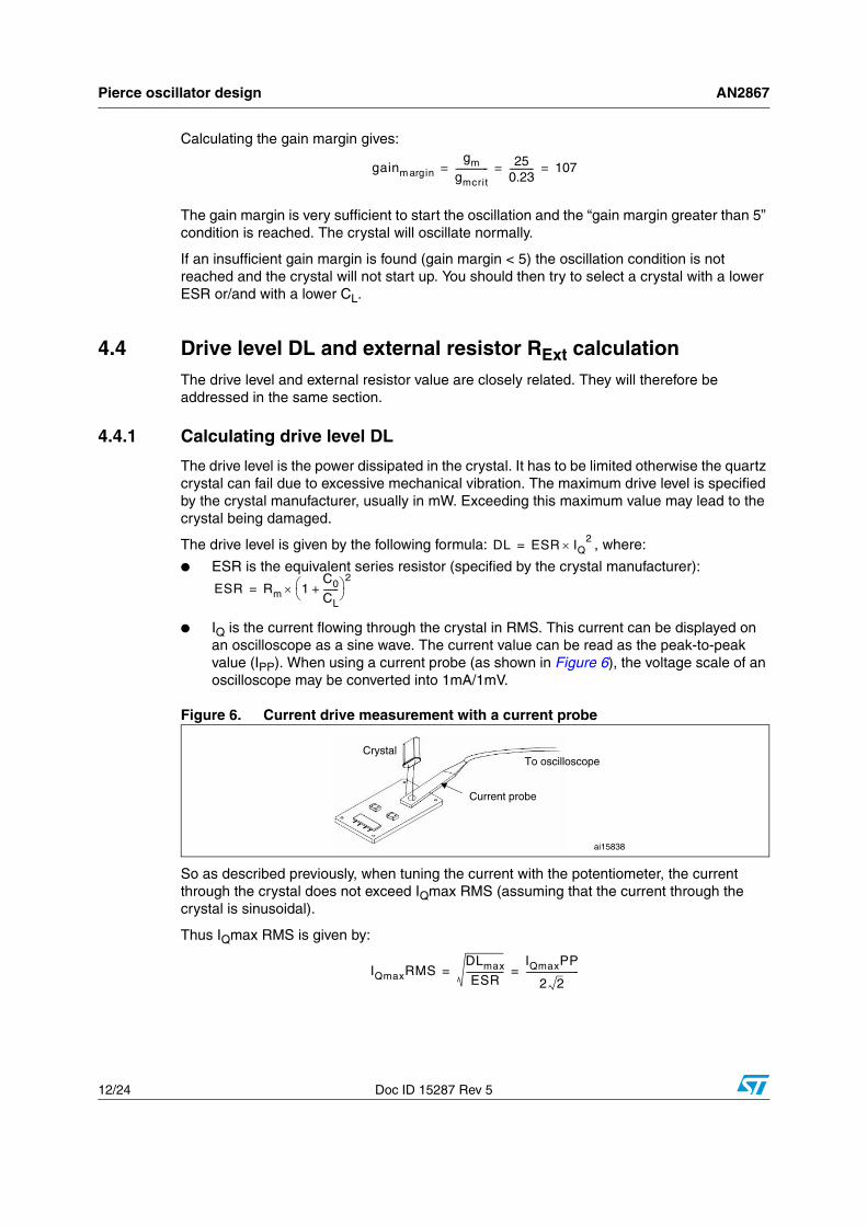
● IQ is the current flowing through the crystal in RMS. This current can be displayed on an oscilloscope as a sine wave. The current value can be read as the peak-to-peak value (IPP). When using a current probe (as shown in Figure 6), the voltage scale of an oscilloscope may be converted into 1mA/1mV.
Figure 6. Current drive measurement with a current probe
So as described previously, when tuning the current with the potentiometer, the current through the crystal does not exceed IQmax RMS (assuming that the current through the crystal is sinusoidal).
Thus IQmax RMS is given by:
gainm inarggm
gmcrit--------------- 25
0.23----------- 107= = =
DL ESR IQ2=
ESR Rm 1C0
CL-------+
2=
Crystal
ai15838
To oscilloscope
Current probe
IQmaxRMSDLmax
ESR-----------------
IQmaxPP
2 2------------------------= =

AN2867 Pierce oscillator design
Doc ID 15287 Rev 5 13/24
Therefore the current through the crystal (peak-to-peak value read on the oscilloscope) should not exceed a maximum peak-to-peak current (IQmaxPP) equal to:
Hence the need for an external resistor (RExt) (refer to Section 4.4.3) when IQ exceeds IQmaxPP. The addition of RExt then becomes mandatory and it is added to ESR in the expression of IQmax.
4.4.2 Another drive level measurement method
The drive level can be computed as:DL= I²QRMS × ESR, where IQRMS is the RMS AC current.
This current can be calculated by measuring the voltage swing at the amplifier input with a low-capacitance oscilloscope probe (no more than 1 pF). The amplifier input current is negligible with respect to the current through CL1, so we can assume that the current through the crystal is equal to the current flowing through CL1. Therefore the RMS voltage at this point is related to the RMS current by:
, with:
● F = crystal frequency
● , where: Vpp is the voltage peak-to-peak measured at CL1 level
● Ctot = CL1 + (Cs/2) + Cprobe where:
– CL1 is the external load capacitor at the amplifier input
– Cs is the stray capacitance
– Cprobe is the probe capacitance)
Therefore the drive level, DL, is given by: .
This DL value must not exceed the drive level specified by the crystal manufacturer.
4.4.3 Calculating external resistor RExt
The role of this resistor is to limit the drive level of the crystal. With CL2, it forms a low-pass filter that forces the oscillator to start at the fundamental frequency and not at overtones (prevents the oscillator from vibrating at 3, 5, 7 etc. times the fundamental frequency). If the power dissipated in the crystal is higher than the value specified by the crystal manufacturer, the external resistor RExt becomes mandatory to avoid overdriving the crystal. If the power dissipated in the selected quartz is less than the drive level specified by the crystal manufacturer, the insertion of RExt is not recommended and its value is then 0 ..
An initial estimation of RExt is obtained by considering the voltage divider formed by RExt/CL2. Thus, the value of RExt is equal to the reactance of CL2.
Therefore: .
Let us put:
● oscillation frequency F = 8 MHz
● CL2 = 15 pF
Then:
IQmaxPP 22 DLmax
ESR---------------------------=
IQRMS 2F VRMS Ctot=
VRMSVpp
2 2-----------=
DLESR F Ctot 2 Vpp 2
2--------------------------------------------------------------------------------=
RExt1
2FC2------------------=
RExt 1326 =
Pierce oscillator design AN2867
14/24 Doc ID 15287 Rev 5
The recommended way of optimizing RExt is to first choose CL1 and CL2 as explained earlier and to connect a potentiometer in the place of RExt. The potentiometer should be initially set to be approximately equal to the capacitive reactance of CL2. It should then be adjusted as required until an acceptable output and crystal drive level are obtained.
Caution: After calculating RExt it is recommended to recalculate the gain margin (refer to Section 4.3: Gain margin of the oscillator) to make sure that the addition of RExt has no effect on the oscillation condition. That is, the value of RExt has to be added to ESR in the expression of gmcrit and gm >> gmcrit must also remain true:
gm >> gmcrit = 4 × (ESR + RExt) × (2 × PI × F)² × (C0 + CL)²
Note: If RExt is too low, there is no power dissipation in the crystal. If RExt is too high, there is no oscillation: the oscillation condition is not reached.
4.5 Startup timeIt is the time that take the oscillations to start and become stable. This time is longer for a quartz than for a ceramic resonator. It depends on the external components: CL1 and CL2. The startup time also depends on the crystal frequency and decreases as the frequency rises. It also depends on the type of crystal used: quartz or ceramic resonator (the startup time for a quartz is very long compared to that of a ceramic resonator). Startup problems are usually due to the gain margin (as explained previously) linked to CL1 and CL2 being too small or too large, or to ESR being too high.
The startup times of crystals for frequencies in the MHz range are within the ms range.
The startup time of a 32 kHz crystal is within the 1 s to 5 s range.
4.6 Crystal pullabilityPullability refers to the change in frequency of a crystal in the area of usual parallel resonance. It is also a measure of its frequency change for a given change in load capacitance. A decrease in load capacitance causes an increase in frequency. Conversely, an increase in load capacitance causes a decrease in frequency. Pullability is given by the following formula:
Pullability PPM pF Cm
610
2 C0 CL+ 2--------------------------------------=

AN2867 Easy guideline for the selection of suitable crystal and external components
Doc ID 15287 Rev 5 15/24
5 Easy guideline for the selection of suitable crystaland external components
This section gives a recommended procedure to select suitable crystal/external components. The whole procedure is divided into three main steps:
Step1: Calculate the gain margin
(please refer to Section 4.3: Gain margin of the oscillator)
● Choose a crystal and go to the references (chosen crystal + microcontroller datasheets)
● Calculate the oscillator gain margin and check if it greater than 5:
If Gain margin < 5, the crystal is not suitable, choose another with a lower ESR or/and a lower CL. Redo step 1.
If Gain margin > 5, go to step 2.
Step2: Calculate the external load capacitors
(please refer to Section 4.2: Load capacitor CL)
Calculate CL1 and CL2 and check if they match the exact capacitor value on market or not:
● If you found the exact capacitor value then the oscillator will oscillate at the exact expected frequency. You can proceed to step 3.
● If you did not find the exact value and:
– frequency accuracy is a key issue for you, you can use a variable capacitor to obtain the exact value. Then you can proceed to step 3.
– frequency accuracy is not critical for you, choose the nearest value found on market and go to step 3.
Step3: Calculate the drive level and external resistor
(please refer to Section 4.4: Drive level DL and external resistor RExt calculation)
● Compute DL and check if is greater or lower than DLcrystal:
– If DL < DLcrystal, no need for an external resistor. Congratulations you have found a suitable crystal.
– If DL > DLcrystal, you should calculate RExt in order to have: DL < DLcrystal. You should then recalculate the gain margin taking RExt into account.If you find that gain margin > 5, congratulations, you have found a suitable crystal. If not, then this crystal will not work and you have to choose another. Return to step 1 to run the procedure for the new crystal.

Some recommended crystals for STM32™ microcontrollers AN2867
16/24 Doc ID 15287 Rev 5
6 Some recommended crystals for STM32™ microcontrollers
6.1 HSE part
6.1.1 Part numbers of recommended 8 MHz crystals
Table 3. EPSON®
Part number ESR CL C0 Gain margin Package
MA-406 or MA-505 or MA-506 (8 MHz) 80 10 pF 5 pF 137.4 SMD
Table 4. HOSONIC ELECTRONIC
Part number ESR CL C0 Gain margin Package
HC-49S-8 MHz 80 10 pF 7 pF 107 Through-hole
Table 5. CTS®
Part number ESR CL C0 Gain margin Package
ATS08A 60 20 pF 7 pF 56.9 Through-hole
ATS08ASM 60 20 pF 7 pF 56.9 SMD
Table 6. FOXElectronics®
Part number ESR CL C0 Gain margin Package
FOXSLF/080-20 80 20 pF 7 pF 43.1 Through-hole
FOXSDLF/080-20 80 20 pF 7 pF 43.1 SMD
PFXLF/080-20 80 20 pF 7 pF 43.1 SMD

AN2867 Some recommended crystals for STM32™ microcontrollers
Doc ID 15287 Rev 5 17/24
6.1.2 Part numbers of recommended ceramic resonators
Table 7 gives the references of recommended CERALOCK® ceramic resonators for the STM32 microcontrollers provided and certified by Murata.
For other Murata resonators recommended for STM32 microcontrollers, please refer to the following link:
http://search.murata.co.jp/Ceramy/ICsearchAction.do?sLang=en.
Then type “STM8” in the “IC part number” and click on “submit query”.
6.1.3 Part numbers of recommended 25 MHz crystals(Ethernet applications)
Table 7. Recommendable conditions (for consumer)
Part number Frequency (MHz) CL (pF)
CSTCR4M00G55-R0 4 39
CSTCE8M00G55-R0 8
33CSTCE8M00G15L**-R0 8 to 13.99
CSTCE12M0G55-R0 12
CSTCE16M0V13L**-R0 14 to 2015
CSTCE16M0V53-R0 16
CSTCW24M0X51R-R0 24 6
Table 8. HOSONIC ELECTRONIC
Part number ESR CL C0 Gain margin Package
6FA25000F10M11 40 10pF 7pF 21.91 SMD
SA25000F10M11 40 10pF 7pF 21.91 Through-hole
Table 9. FOXElectronics®
Part number ESR CL C0 Gain margin Package
FOXSLF/250F-20 30 20 pF 7 pF 11.58 Through-hole
FOXSDLF/250F-20 30 20 pF 7 pF 11.58 SMD
PFXLF250F-20 30 20 pF 7 pF 11.58 SMD
Table 10. CTS®
Part number ESR CL C0 Gain margin Package
ATS25A 30 20 pF 7 pF 11.58 Through-hole
ATS25ASM 30 20 pF 7 pF 11.58 SMD

Some recommended crystals for STM32™ microcontrollers AN2867
18/24 Doc ID 15287 Rev 5
6.1.4 Part numbers of recommended 14.7456 MHz crystals (audioapplications)
Table 11. FOXElectronics®
Part number ESR CL C0 Gain margin Package
FOXSLF/147-20 40 20 pF 7 pF 24.97 Through-hole
FOXSDLF/147-20 40 20 pF 7 pF 24.97 SMD
Table 12. ABRACON™
Part number ESR CL C0 Gain margin Package
ABMM2-14.7456 MHz 50 18 pF 7 pF 29.3 SMD

AN2867 Some recommended crystals for STM32™ microcontrollers
Doc ID 15287 Rev 5 19/24
6.2 LSE partFor the low-speed external oscillator (LSE) part of STM32 microcontrollers, it is recommended to use a crystal with CL 7 pF.
Table 13. Recommendable crystals
ManufacturerQuartz reference/
part numberCL
(pF)ESR
(Ohm)Frequency
(Hz)C0
(pF)Gm
margin
Abracon ABS07 7 70000 32768 1.05 6.5
Abracon AB206J 6 50000 32768 1.35 10.9
Abracon ABS25 6 50000 32768 1.35 10.9
Abracon AB26TRB 6 50000 32768 1.35 10.9
Abracon AB26TRJ 6 40000 32768 1.1 14.6
ACT ACT4115A SMX 7 70000 32768 1.1 6.4
ACT ACT3215A SMX 7 70000 32768 0.95 6.7
ACT ACT711S 7 65000 32768 0.8 7.5
ACT ACT201 7 50000 32768 1 9.2
ACT ACT201 6 50000 32768 1 12.0
ACT ACT200A 6 50000 32768 0.9 12.4
EPSON FC135/145 7 70000 32768 1 6.6
EPSON MC146/156 7 65000 32768 0.8 7.5
EPSON C-002RX 6 60000 32768 0.85 10.5
EPSON MC306/405/406 6 50000 32768 0.9 12.4
EPSON MC30A 6 50000 32768 0.9 12.4
EPSON C-004R 6 50000 32768 0.85 12.6
EPSON C-005R 6 50000 32768 0.75 12.9
EPSON C-001R 6 35000 32768 0.9 17.7
JFVNY DT-38G06 6 30000 32768 1.3 18.44
JFVNY MC306G06 6 50000 32768 2 9.3
KYOCERA ST3215SB32768C0HPWBB 7 70000 32768 0.9 6.7
MicroCrystal MS1V-T1K 6 60000 32768 0.9 10.3

Some recommended crystals for STM8A/S microcontrollers AN2867
20/24 Doc ID 15287 Rev 5
7 Some recommended crystals for STM8A/S microcontrollers
7.1 Part numbers of recommended crystal oscillators
7.2 Part numbers of recommended ceramic resonatorsTable 15 and Table 16 give the references of recommended CERALOCK® ceramic resonators for the STM8A microcontrollers provided and certified by Murata.
Table 14. KYOCERA
Part number Freq. ESR CL Drive level (DL)
CX5032GA08000H0QSWZZ 8 MHz 300 max 12 pF 500 µW max
CX5032GA16000H0QSWZZ 16 MHz 100 max 12 pF 300 µW max
CX8045GA08000H0QSWZZ 8 MHz 200 max 12 pF 500 µW max
CX8045GA16000H0QSWZZ 16 MHz 50 max 12 pF 300 µW max
Table 15. Recommendable conditions (for consumer)
Part number Freq. CL
CSTCR4M00G55B-R0 4 MHz CL1 = CL2 = 39 pF
CSTCE8M00G55A-R0 8 MHz CL1 = CL2 = 33 pF
CSTCE16M0V53-R0 16 MHz CL1 = CL2 = 15 pF
Table 16. Recommendable conditions (for CAN-BUS)
Part number Freq. CL
CSTCR4M00G15C**-R0 4 MHz CL1 = CL2 = 39 pF
CSTCR8M00G15C**-R0 8 MHz CL1 = CL2 = 33 pF
CSTCE16M0V13C**-R0 16 MHz CL1 = CL2 = 15 pF
AN2867 Some PCB hints
Doc ID 15287 Rev 5 21/24
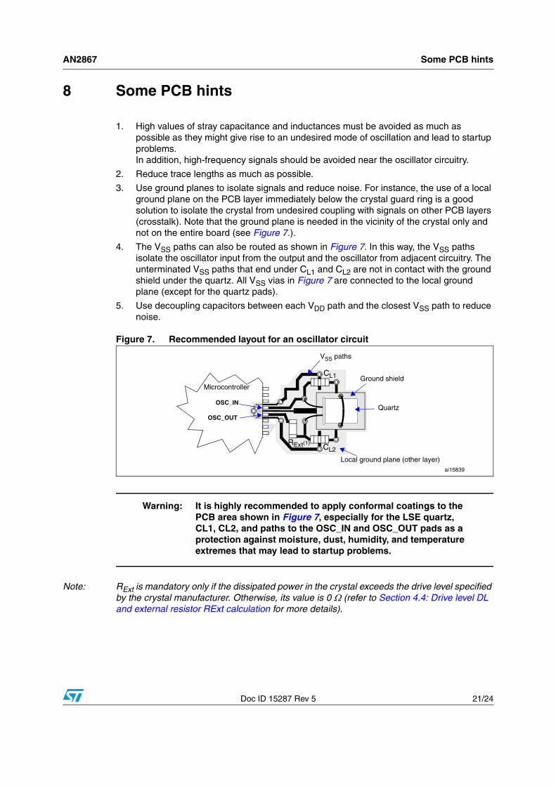
8 Some PCB hints
1. High values of stray capacitance and inductances must be avoided as much as possible as they might give rise to an undesired mode of oscillation and lead to startup problems.In addition, high-frequency signals should be avoided near the oscillator circuitry.
2. Reduce trace lengths as much as possible.
3. Use ground planes to isolate signals and reduce noise. For instance, the use of a local ground plane on the PCB layer immediately below the crystal guard ring is a good solution to isolate the crystal from undesired coupling with signals on other PCB layers (crosstalk). Note that the ground plane is needed in the vicinity of the crystal only and not on the entire board (see Figure 7.).
4. The VSS paths can also be routed as shown in Figure 7. In this way, the VSS paths isolate the oscillator input from the output and the oscillator from adjacent circuitry. The unterminated VSS paths that end under CL1 and CL2 are not in contact with the ground shield under the quartz. All VSS vias in Figure 7 are connected to the local ground plane (except for the quartz pads).
5. Use decoupling capacitors between each VDD path and the closest VSS path to reduce noise.
Figure 7. Recommended layout for an oscillator circuit
Warning: It is highly recommended to apply conformal coatings to the PCB area shown in Figure 7, especially for the LSE quartz, CL1, CL2, and paths to the OSC_IN and OSC_OUT pads as a protection against moisture, dust, humidity, and temperature extremes that may lead to startup problems.
Note: RExt is mandatory only if the dissipated power in the crystal exceeds the drive level specified by the crystal manufacturer. Otherwise, its value is 0 (refer to Section 4.4: Drive level DL and external resistor RExt calculation for more details).
CL2RExt(1)
OSC_OUT
OSC_IN
Microcontroller
CL1 Ground shield
ai15839
VSS paths
Quartz
Local ground plane (other layer)

Conclusion AN2867
22/24 Doc ID 15287 Rev 5
9 Conclusion
The most important parameter is the gain margin of the oscillator, which determines if the oscillator will start up or not. This parameter has to be calculated at the beginning of the design phase to choose the suitable crystal for the application. The second parameter is the value of the external load capacitors that have to be selected in accordance with the CL specification of the crystal (provided by the crystal manufacturer). This determines the frequency accuracy of the crystal. The third parameter is the value of the external resistor that is used to limit the drive level. In the 32 kHz oscillator part, however, it is not recommended to use an external resistor.
Because of the number of variables involved, in the experimentation phase you should use components that have exactly the same properties as those that will be used in production. Likewise, you should work with the same oscillator layout and in the same environment to avoid unexpected behavior and therefore save time.

AN2867 Revision history
Doc ID 15287 Rev 5 23/24
10 Revision history
Table 17. Document revision history
Date Revision Changes
20-Jan-2009 1 Initial release.
10-Nov-2009 2
DL formula corrected in Section 4.4.2: Another drive level measurement method.
Package column added to all tables in Section 6: Some recommended crystals for STM32™ microcontrollers.
Recommended part numbers updated in Section 6.1: HSE part and Section 6.2: LSE part.
Section 6.1.3: Part numbers of recommended 25 MHz crystals (Ethernet applications) added.
Section 6.1.4: Part numbers of recommended 14.7456 MHz crystals (audio applications) added.
27-Apr-2010 3Added Section 7: Some recommended crystals for STM8A/S microcontrollers.
25-Nov-2010 4
Updated Section 6.1.2: Part numbers of recommended ceramic resonators: removed Table 7: Recommendable condition (for consumer) and Table 8: Recommendable condition (for CAN bus); added Table 7: Recommendable conditions (for consumer); updated murata resonator link.Updated Section 6.2: LSE part: removed Table 13: EPSON TOYOCOM, Table 14: JFVNY®, and Table 15: KDS; Added Table 13: Recommendable crystals.
Added Warning: after Figure 7.
30-Mar-2011 5
Section 6.1.2: Part numbers of recommended ceramic resonators: updated “STM32” with “STM8”.
Table 15: Recommendable conditions (for consumer): replaced ceramic resonator part number “CSTSE16M0G55A-R0” by “CSTCE16M0V53-R0”.

AN2867
24/24 Doc ID 15287 Rev 5
Please Read Carefully:
Information in this document is provided solely in connection with ST products. STMicroelectronics NV and its subsidiaries (“ST”) reserve theright to make changes, corrections, modifications or improvements, to this document, and the products and services described herein at anytime, without notice.
All ST products are sold pursuant to ST’s terms and conditions of sale.
Purchasers are solely responsible for the choice, selection and use of the ST products and services described herein, and ST assumes noliability whatsoever relating to the choice, selection or use of the ST products and services described herein.
No license, express or implied, by estoppel or otherwise, to any intellectual property rights is granted under this document. If any part of thisdocument refers to any third party products or services it shall not be deemed a license grant by ST for the use of such third party productsor services, or any intellectual property contained therein or considered as a warranty covering the use in any manner whatsoever of suchthird party products or services or any intellectual property contained therein.
UNLESS OTHERWISE SET FORTH IN ST’S TERMS AND CONDITIONS OF SALE ST DISCLAIMS ANY EXPRESS OR IMPLIEDWARRANTY WITH RESPECT TO THE USE AND/OR SALE OF ST PRODUCTS INCLUDING WITHOUT LIMITATION IMPLIEDWARRANTIES OF MERCHANTABILITY, FITNESS FOR A PARTICULAR PURPOSE (AND THEIR EQUIVALENTS UNDER THE LAWSOF ANY JURISDICTION), OR INFRINGEMENT OF ANY PATENT, COPYRIGHT OR OTHER INTELLECTUAL PROPERTY RIGHT.
UNLESS EXPRESSLY APPROVED IN WRITING BY AN AUTHORIZED ST REPRESENTATIVE, ST PRODUCTS ARE NOTRECOMMENDED, AUTHORIZED OR WARRANTED FOR USE IN MILITARY, AIR CRAFT, SPACE, LIFE SAVING, OR LIFE SUSTAININGAPPLICATIONS, NOR IN PRODUCTS OR SYSTEMS WHERE FAILURE OR MALFUNCTION MAY RESULT IN PERSONAL INJURY,DEATH, OR SEVERE PROPERTY OR ENVIRONMENTAL DAMAGE. ST PRODUCTS WHICH ARE NOT SPECIFIED AS "AUTOMOTIVEGRADE" MAY ONLY BE USED IN AUTOMOTIVE APPLICATIONS AT USER’S OWN RISK.
Resale of ST products with provisions different from the statements and/or technical features set forth in this document shall immediately voidany warranty granted by ST for the ST product or service described herein and shall not create or extend in any manner whatsoever, anyliability of ST.
ST and the ST logo are trademarks or registered trademarks of ST in various countries.
Information in this document supersedes and replaces all information previously supplied.
The ST logo is a registered trademark of STMicroelectronics. All other names are the property of their respective owners.
© 2011 STMicroelectronics - All rights reserved
STMicroelectronics group of companies
Australia - Belgium - Brazil - Canada - China - Czech Republic - Finland - France - Germany - Hong Kong - India - Israel - Italy - Japan - Malaysia - Malta - Morocco - Philippines - Singapore - Spain - Sweden - Switzerland - United Kingdom - United States of America
www.st.com