Embed Size (px)
Citation preview
1
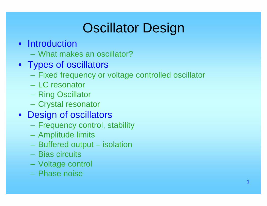
Oscillator Design• Introduction
– What makes an oscillator?• Types of oscillators
– Fixed frequency or voltage controlled oscillator– LC resonator– Ring Oscillator– Crystal resonator
• Design of oscillators– Frequency control, stability– Amplitude limits– Buffered output – isolation– Bias circuits– Voltage control– Phase noise
2
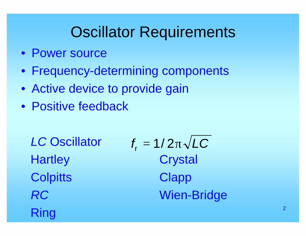
Oscillator Requirements• Power source• Frequency-determining components• Active device to provide gain• Positive feedback
LC OscillatorHartley CrystalColpitts ClappRC Wien-BridgeRing
LCf π= 2/1r
3
Feedback Model for oscillators( ) ( )
( ) ( )ωω jjAjAjAf β⋅−ω
=ω1
( ) ( ) 1ωcriteria Barkhausen=⋅ jjA βω
A
β
ix ox
fx
fid xxx +=
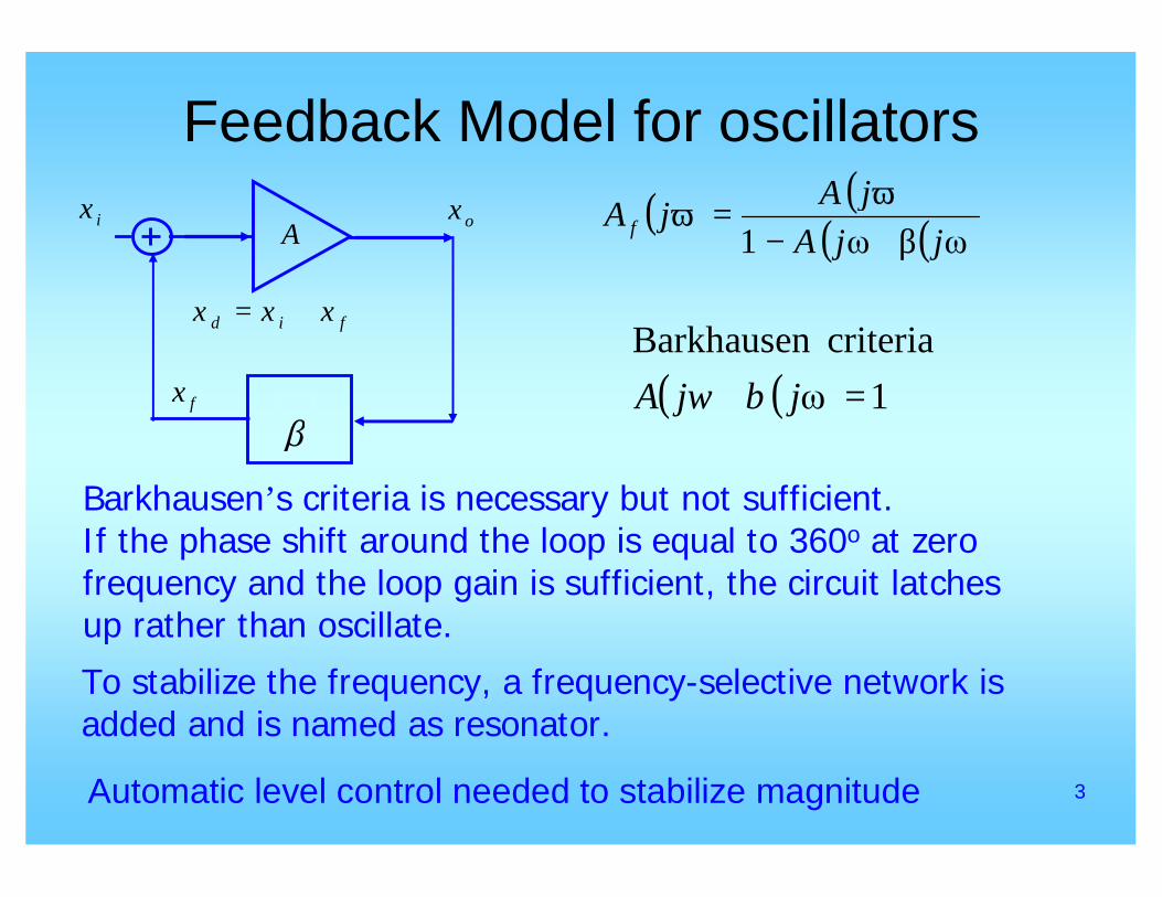
Barkhausen’s criteria is necessary but not sufficient.If the phase shift around the loop is equal to 360o at zero frequency and the loop gain is sufficient, the circuit latches up rather than oscillate.
To stabilize the frequency, a frequency-selective network is added and is named as resonator.
Automatic level control needed to stabilize magnitude
4
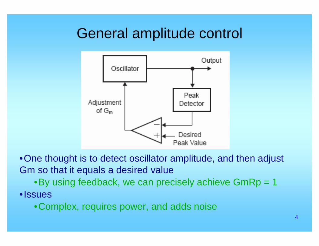
General amplitude control
•One thought is to detect oscillator amplitude, and then adjust Gm so that it equals a desired value
•By using feedback, we can precisely achieve GmRp = 1•Issues
•Complex, requires power, and adds noise
5
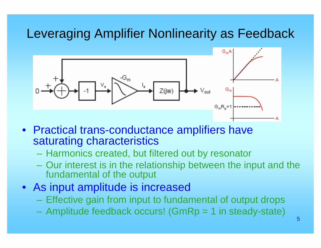
Leveraging Amplifier Nonlinearity as Feedback
• Practical trans-conductance amplifiers have saturating characteristics – Harmonics created, but filtered out by resonator – Our interest is in the relationship between the input and the
fundamental of the output• As input amplitude is increased
– Effective gain from input to fundamental of output drops – Amplitude feedback occurs! (GmRp = 1 in steady-state)
6
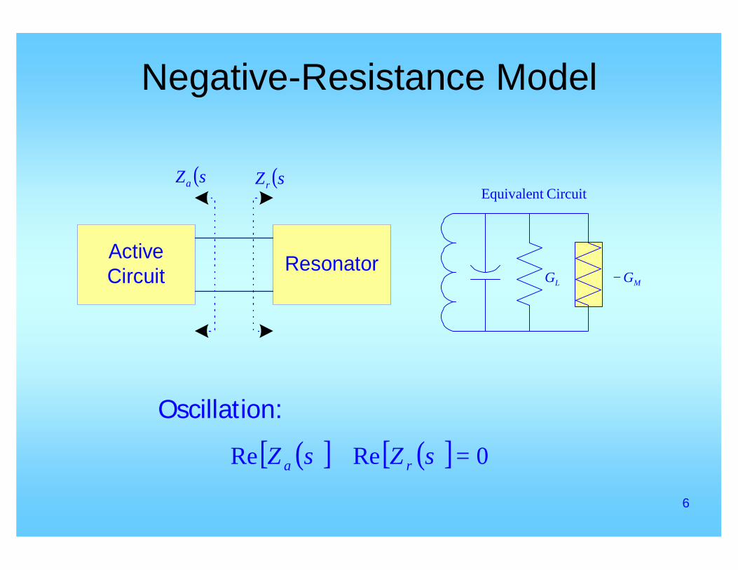
Negative-Resistance Model
ActiveCircuit Resonator
( )sZa ( )sZr
( )[ ] ( )[ ] 0ReRe =+ sZsZ ra
LG MG−
Circuit Equivalent
Oscillation:
7
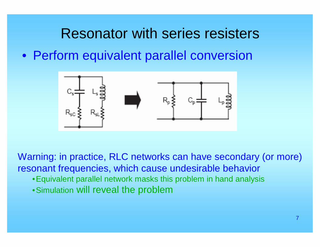
Resonator with series resisters• Perform equivalent parallel conversion
Warning: in practice, RLC networks can have secondary (or more) resonant frequencies, which cause undesirable behavior
•Equivalent parallel network masks this problem in hand analysis•Simulation will reveal the problem
8
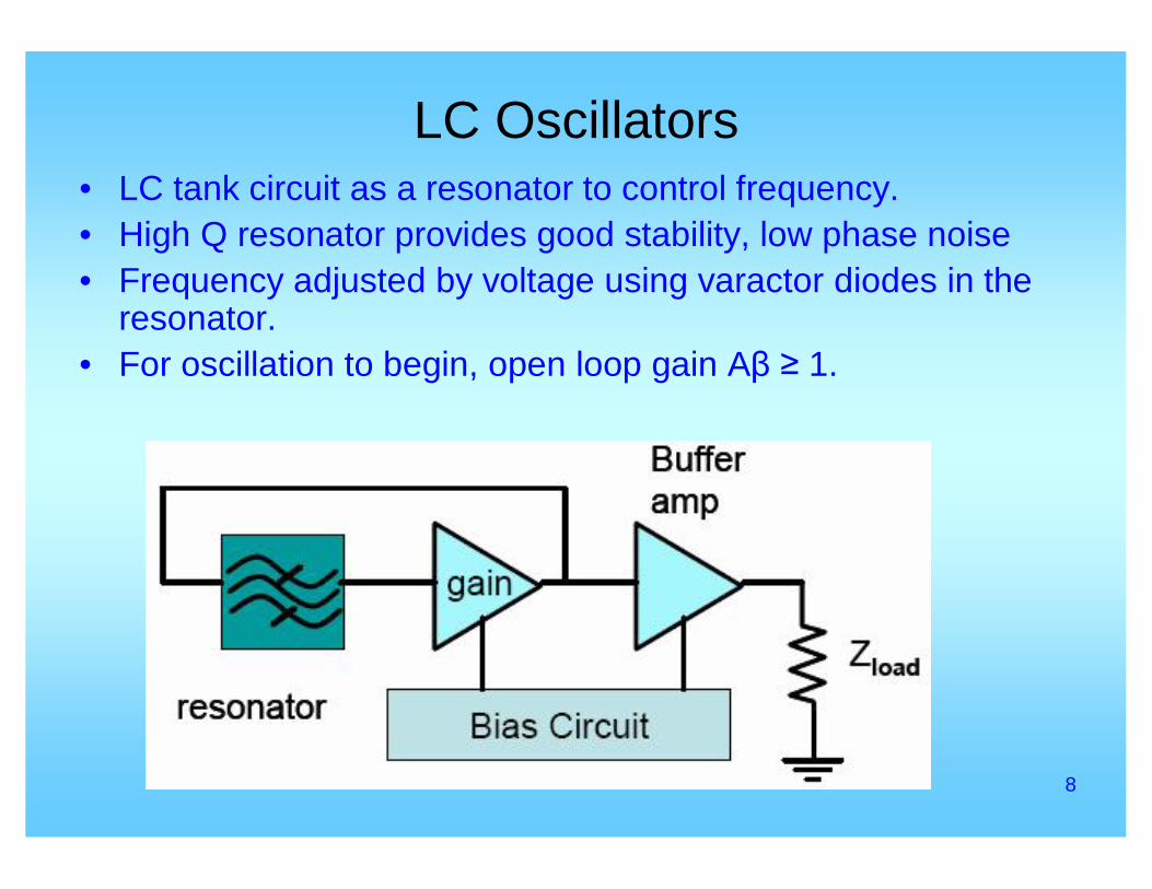
LC Oscillators• LC tank circuit as a resonator to control frequency.• High Q resonator provides good stability, low phase noise• Frequency adjusted by voltage using varactor diodes in the
resonator.• For oscillation to begin, open loop gain Aβ ≥ 1.
9
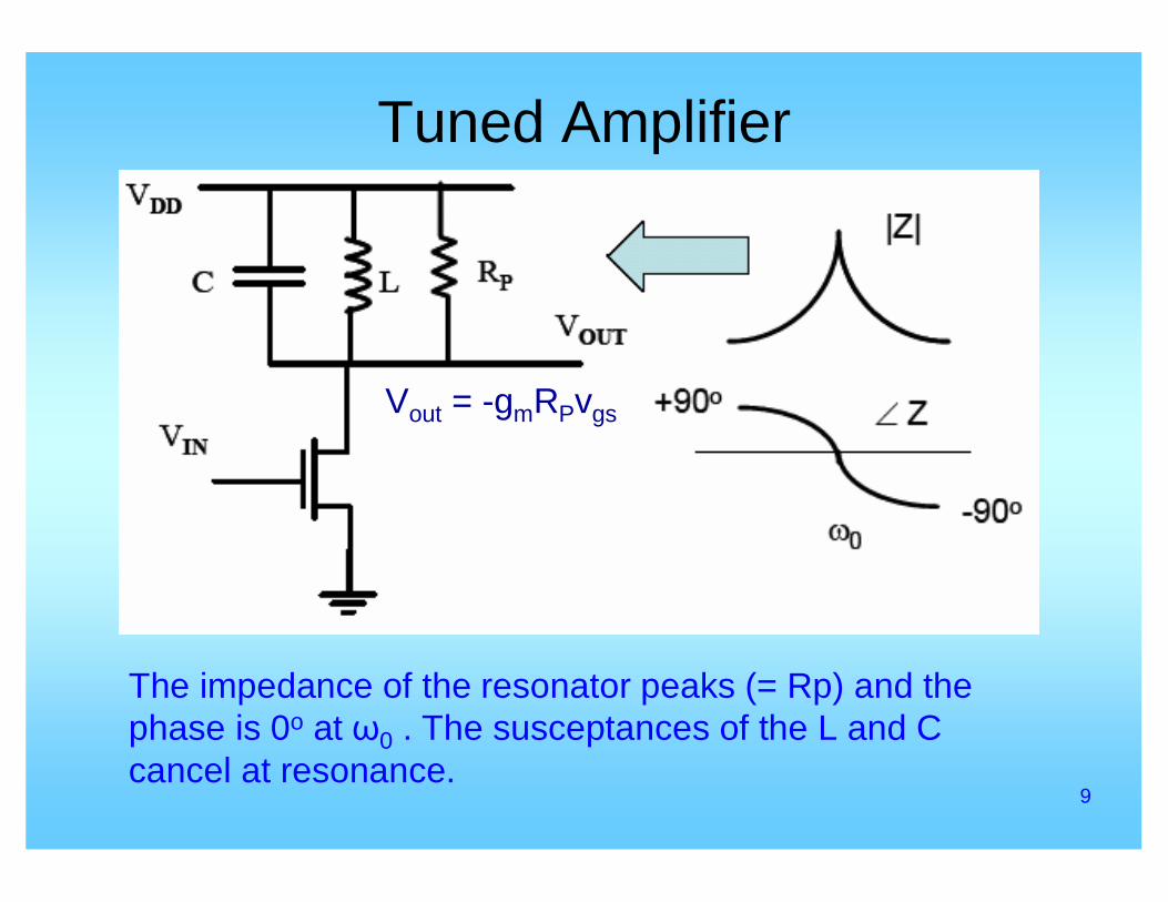
Tuned Amplifier
The impedance of the resonator peaks (= Rp) and the phase is 0o at ω0 . The susceptances of the L and C cancel at resonance.
Vout = -gmRPvgs
10
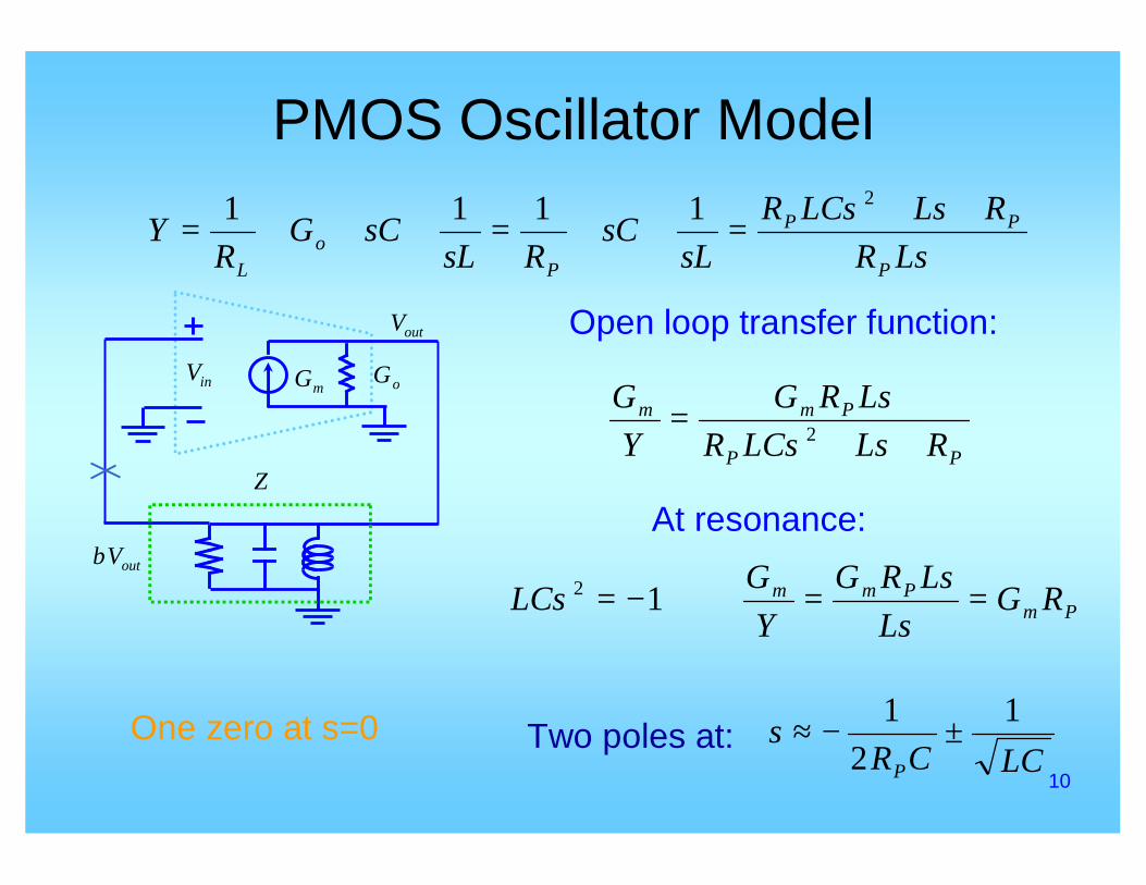
PMOS Oscillator Model
LsRRLsLCsR
sLsC
RsLsCG
RY
P
PP
Po
L
++=++=+++=
21111
mGinV
outVβ
outV
oG
Z
Open loop transfer function:
PP
Pmm
RLsLCsRLsRG
YG
++= 2
At resonance:
PmPmm RG
LsLsRG
YGLCs ==−= 12
One zero at s=0 Two poles at: LCCR
sP
12
1±−≈
11
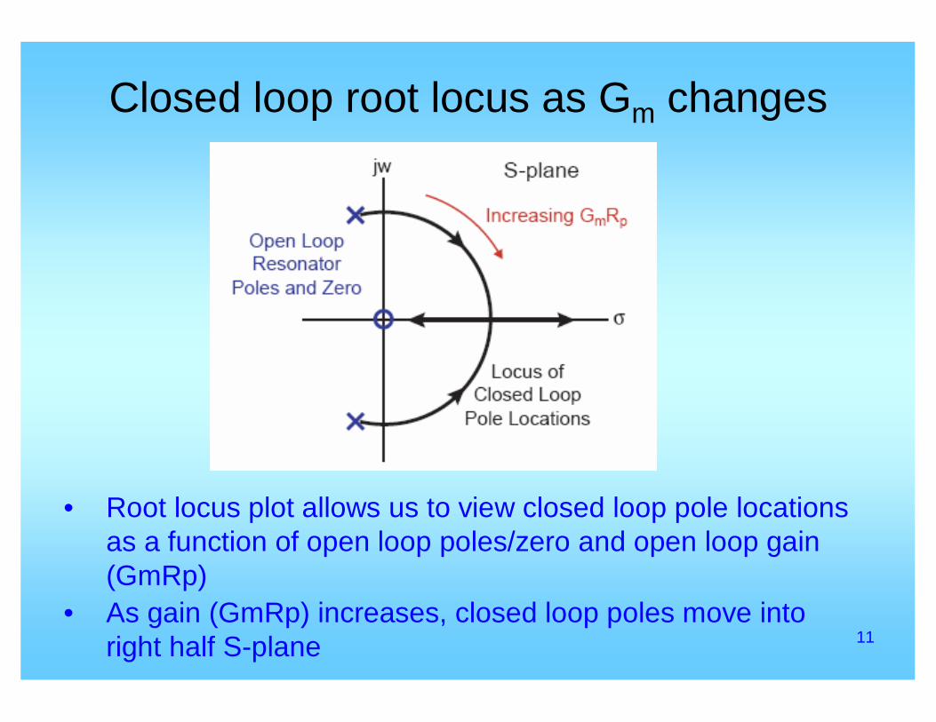
Closed loop root locus as Gm changes
• Root locus plot allows us to view closed loop pole locations as a function of open loop poles/zero and open loop gain (GmRp)
• As gain (GmRp) increases, closed loop poles move into right half S-plane
12
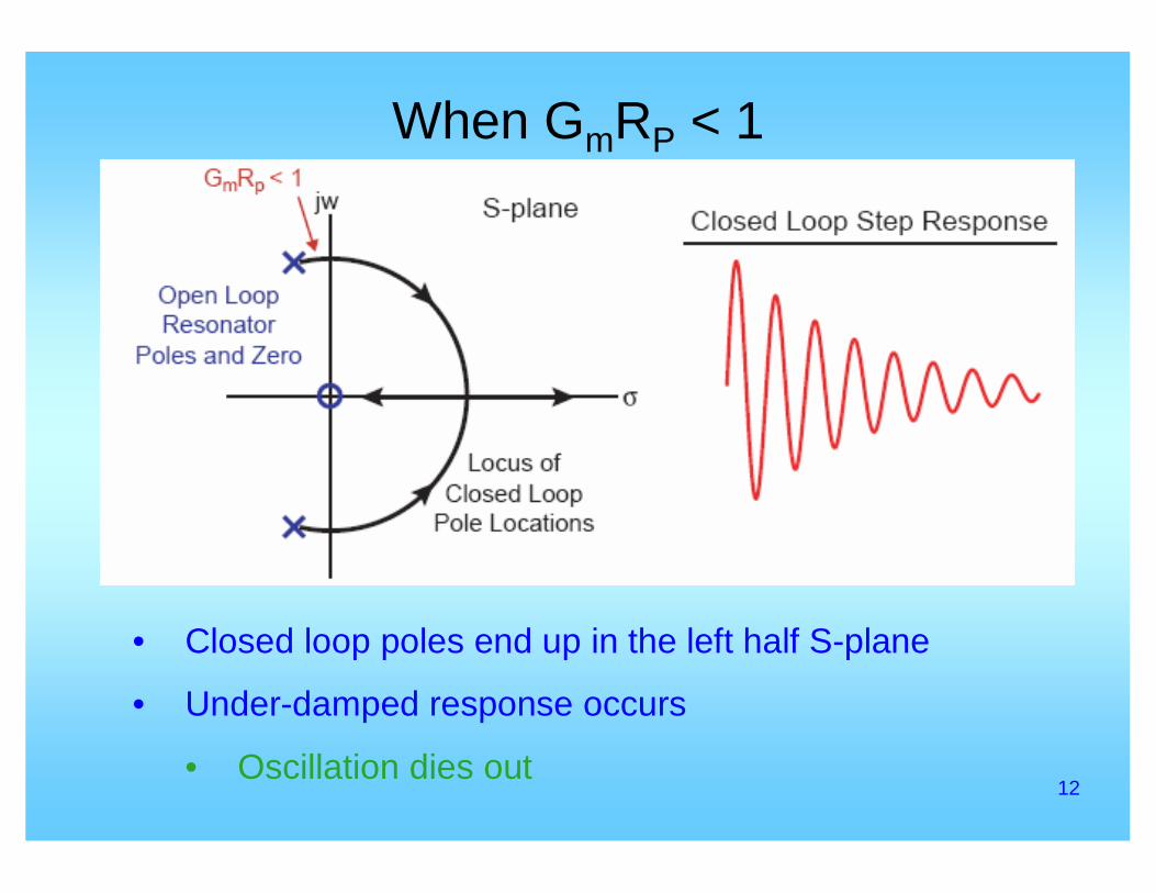
When GmRP < 1
• Closed loop poles end up in the left half S-plane
• Under-damped response occurs
• Oscillation dies out
13
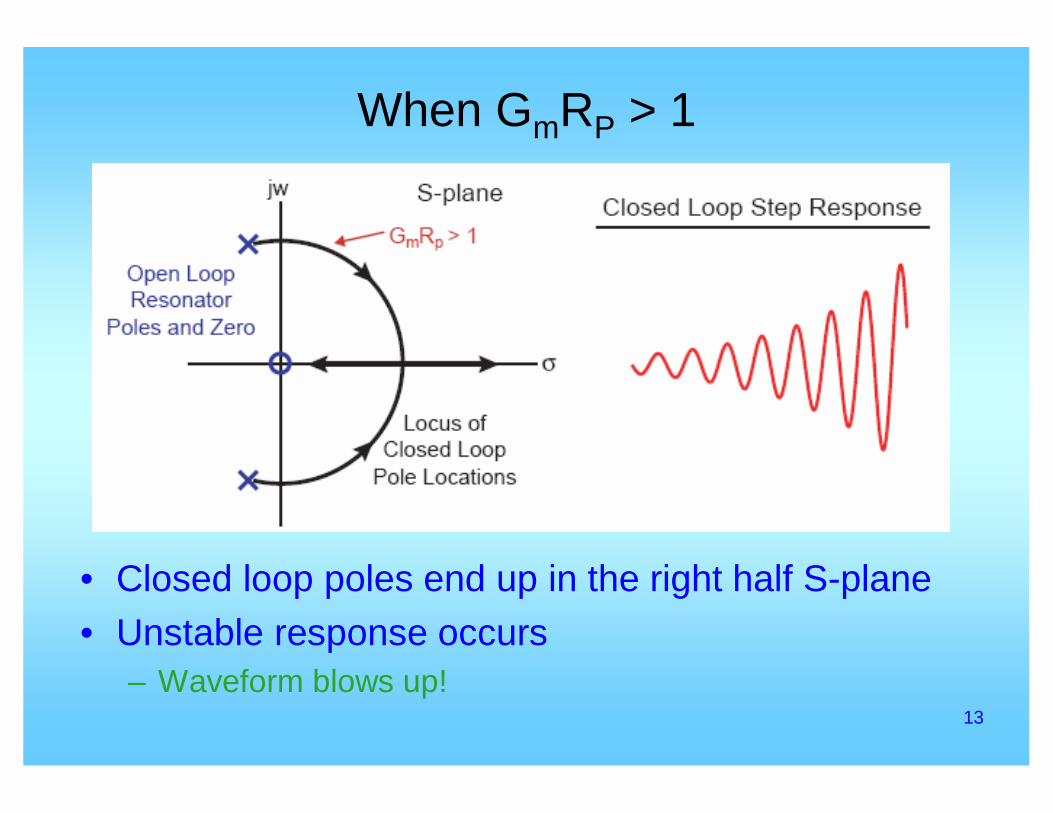
When GmRP > 1
• Closed loop poles end up in the right half S-plane • Unstable response occurs
– Waveform blows up!
14
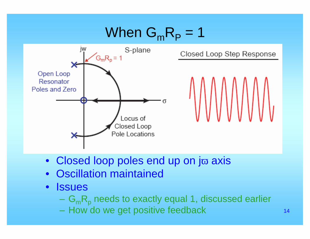
When GmRP = 1
• Closed loop poles end up on jω axis • Oscillation maintained• Issues
– GmRp needs to exactly equal 1, discussed earlier– How do we get positive feedback
15
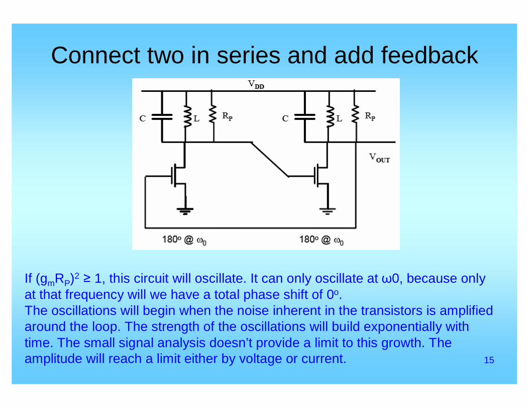
Connect two in series and add feedback
If (gmRP)2 ≥ 1, this circuit will oscillate. It can only oscillate at ω0, because only at that frequency will we have a total phase shift of 0o.The oscillations will begin when the noise inherent in the transistors is amplified around the loop. The strength of the oscillations will build exponentially with time. The small signal analysis doesn’t provide a limit to this growth. The amplitude will reach a limit either by voltage or current.
16
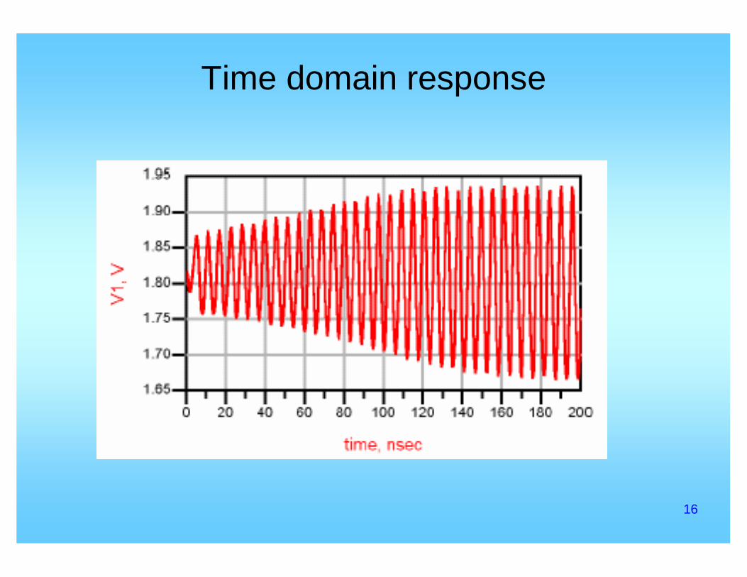
Time domain response
17
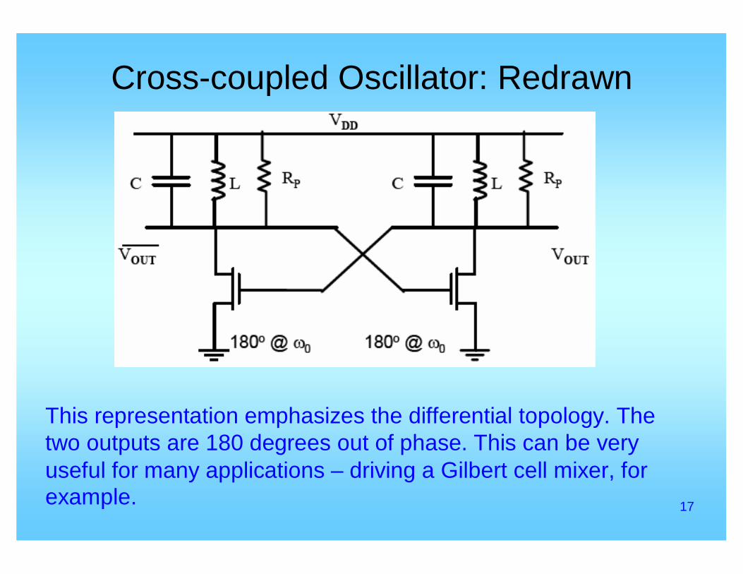
Cross-coupled Oscillator: Redrawn
This representation emphasizes the differential topology. The two outputs are 180 degrees out of phase. This can be very useful for many applications – driving a Gilbert cell mixer, for example.
18
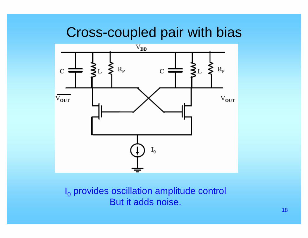
Cross-coupled pair with bias
I0 provides oscillation amplitude controlBut it adds noise.
19
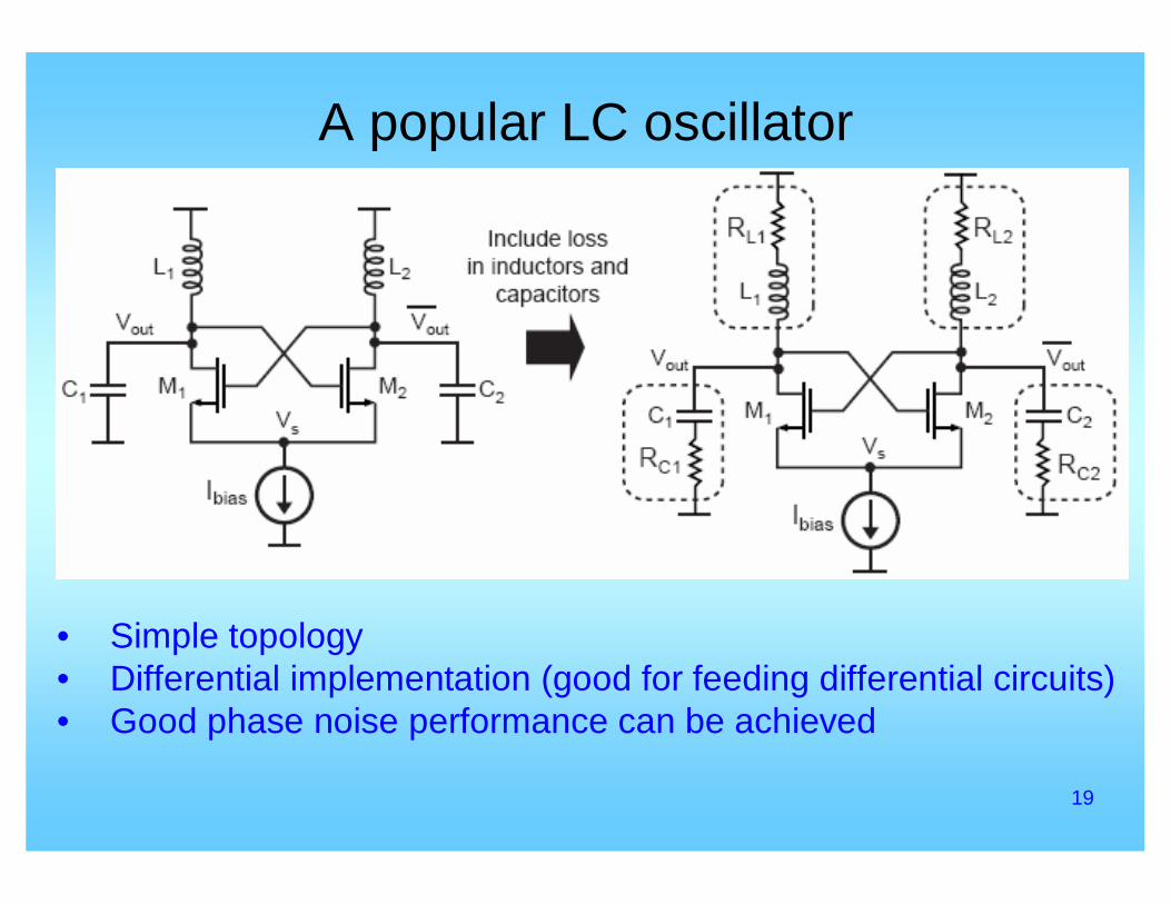
A popular LC oscillator
• Simple topology • Differential implementation (good for feeding differential circuits) • Good phase noise performance can be achieved
20
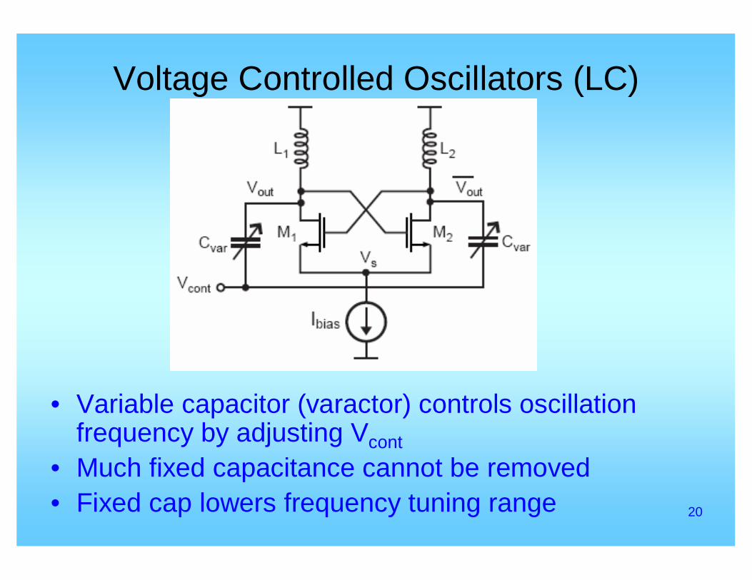
Voltage Controlled Oscillators (LC)
• Variable capacitor (varactor) controls oscillation frequency by adjusting Vcont
• Much fixed capacitance cannot be removed• Fixed cap lowers frequency tuning range
21
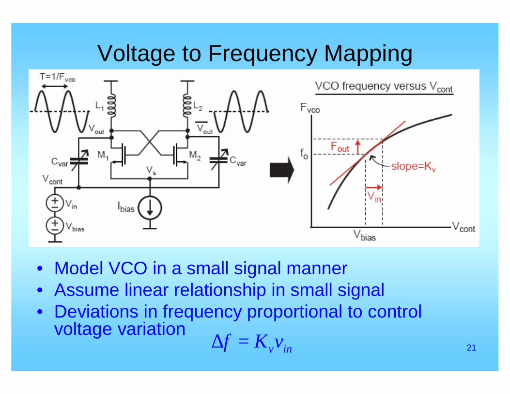
Voltage to Frequency Mapping
• Model VCO in a small signal manner• Assume linear relationship in small signal• Deviations in frequency proportional to control
voltage variationinvvKf =∆
22
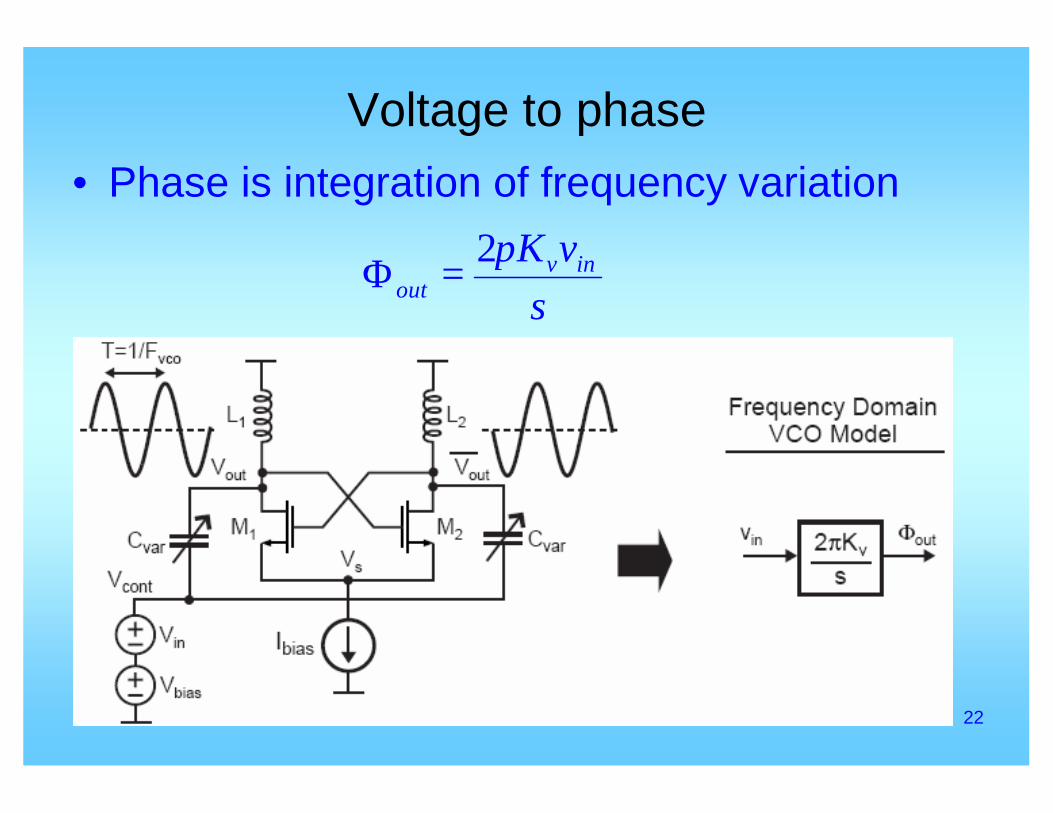
Voltage to phase• Phase is integration of frequency variation
svK inv
outπ2
=Φ
23
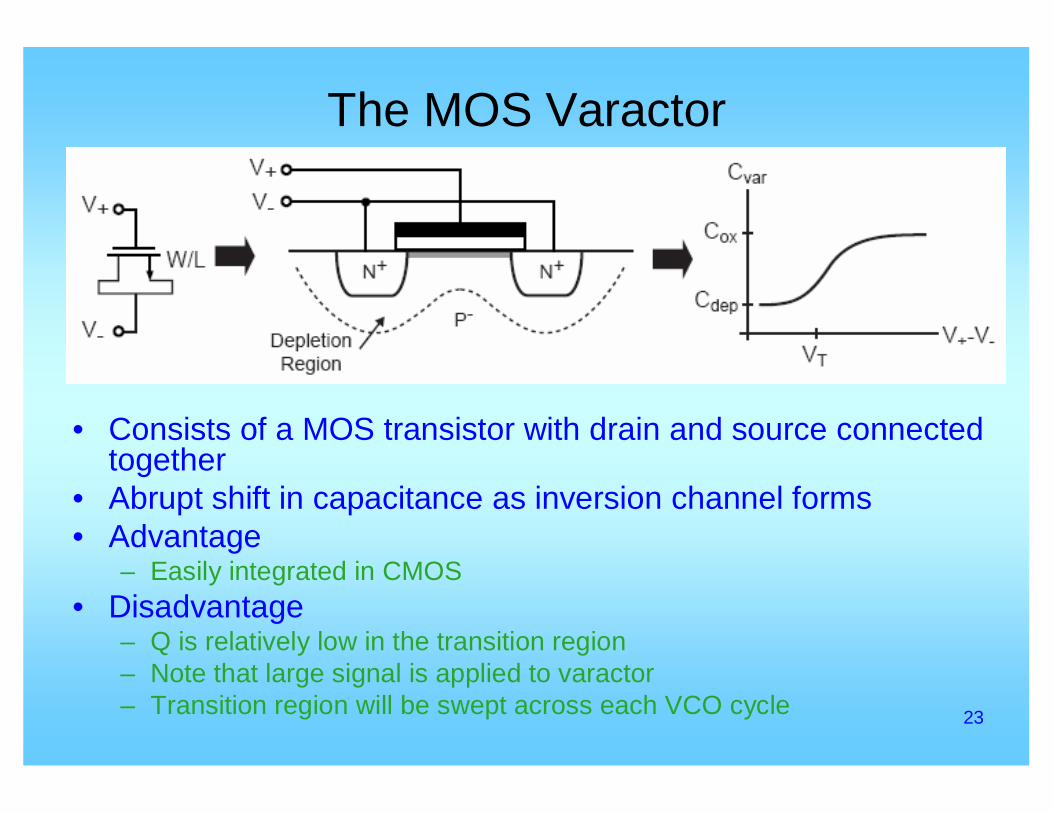
The MOS Varactor
• Consists of a MOS transistor with drain and source connected together
• Abrupt shift in capacitance as inversion channel forms • Advantage
– Easily integrated in CMOS • Disadvantage
– Q is relatively low in the transition region– Note that large signal is applied to varactor– Transition region will be swept across each VCO cycle
24
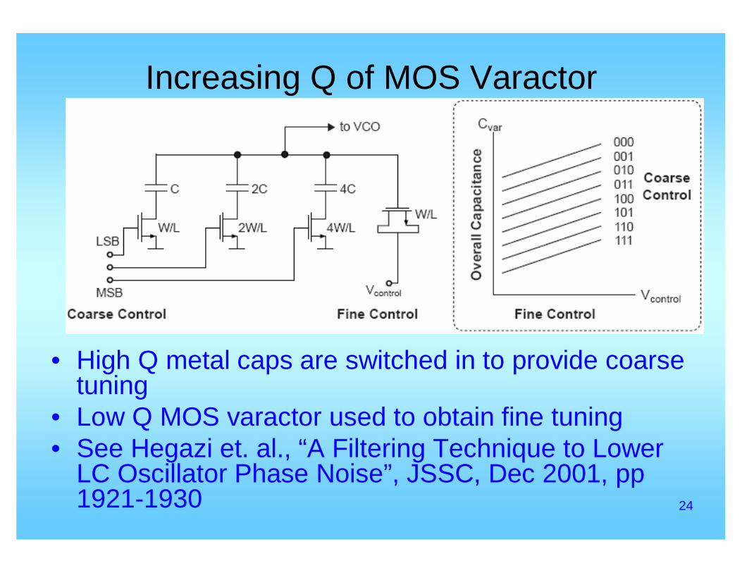
Increasing Q of MOS Varactor
• High Q metal caps are switched in to provide coarse tuning
• Low Q MOS varactor used to obtain fine tuning • See Hegazi et. al., “A Filtering Technique to Lower
LC Oscillator Phase Noise”, JSSC, Dec 2001, pp 1921-1930
25
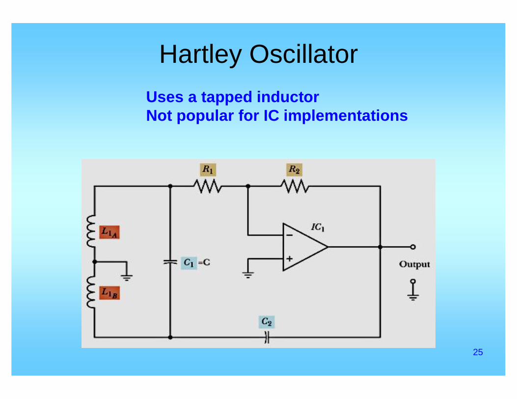
Hartley OscillatorUses a tapped inductorNot popular for IC implementations
26
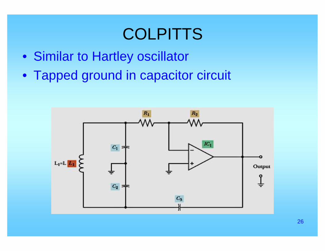
COLPITTS• Similar to Hartley oscillator• Tapped ground in capacitor circuit
27
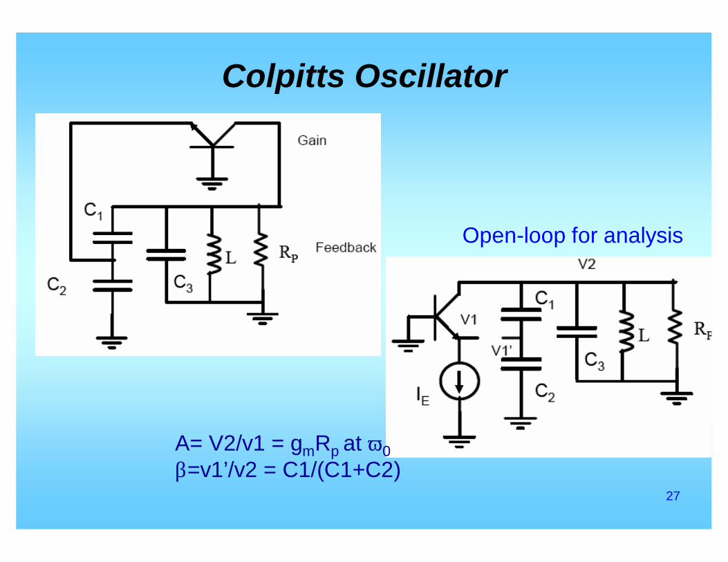
Colpitts Oscillator
Open-loop for analysis
A= V2/v1 = gmRp at ω0β=v1’/v2 = C1/(C1+C2)
28
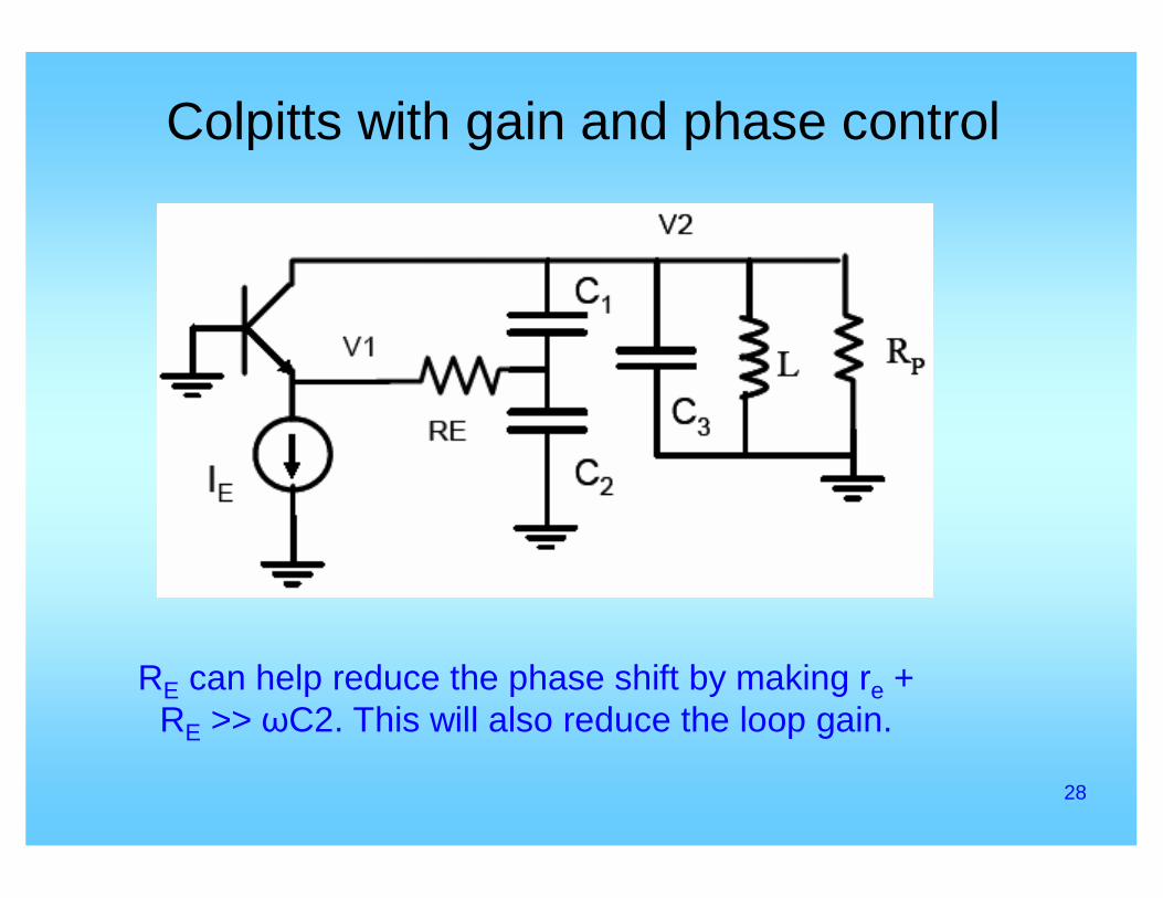
Colpitts with gain and phase control
RE can help reduce the phase shift by making re + RE >> ωC2. This will also reduce the loop gain.
29
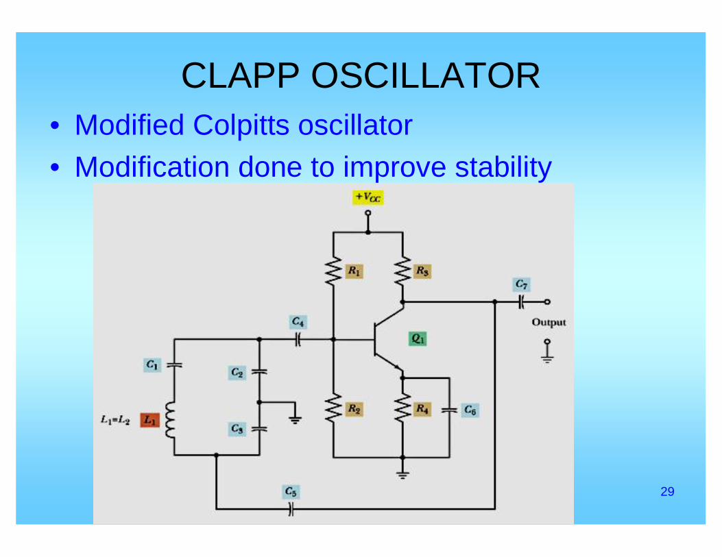
CLAPP OSCILLATOR• Modified Colpitts oscillator• Modification done to improve stability
30
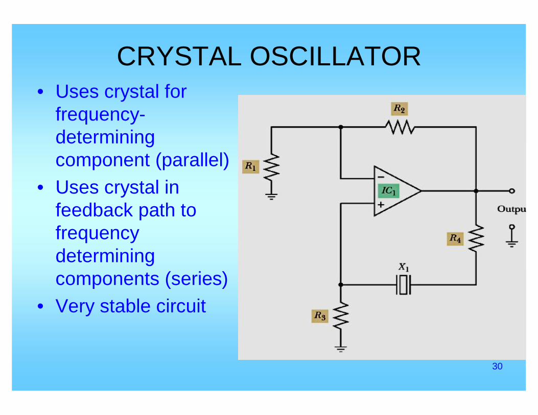
CRYSTAL OSCILLATOR• Uses crystal for
frequency-determining component (parallel)
• Uses crystal in feedback path to frequency determining components (series)
• Very stable circuit
31
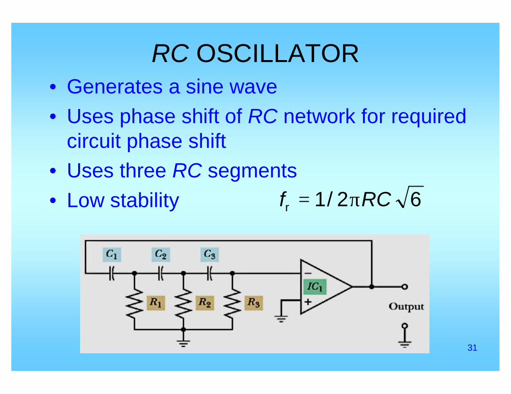
RC OSCILLATOR• Generates a sine wave• Uses phase shift of RC network for required
circuit phase shift• Uses three RC segments• Low stability 62/1r RCf π=
32
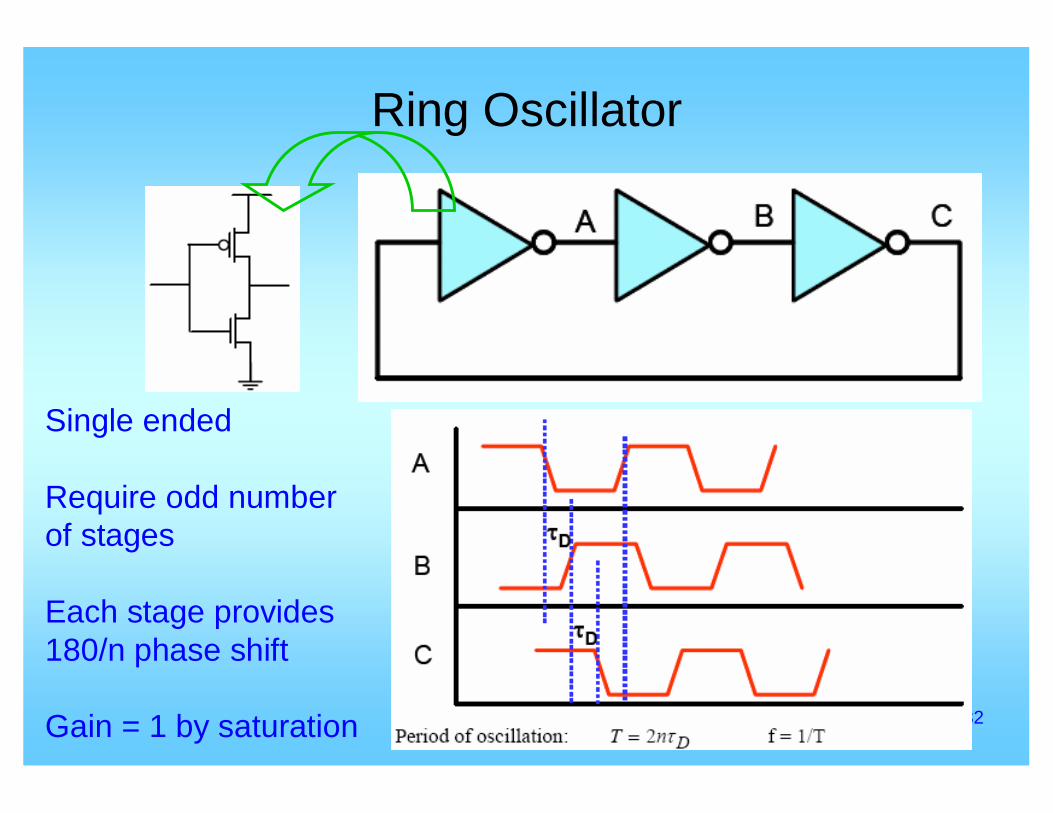
Ring Oscillator
Single ended
Require odd number of stages
Each stage provides 180/n phase shift
Gain = 1 by saturation
33
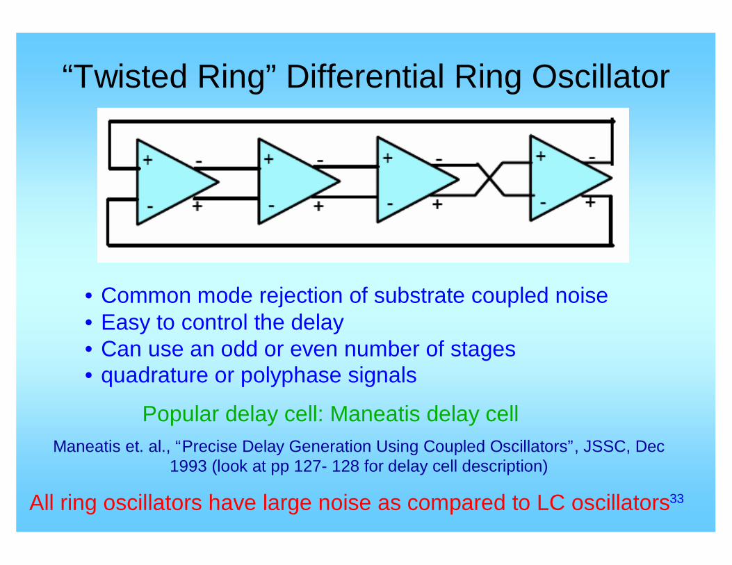
“Twisted Ring” Differential Ring Oscillator
• Common mode rejection of substrate coupled noise• Easy to control the delay• Can use an odd or even number of stages• quadrature or polyphase signals
All ring oscillators have large noise as compared to LC oscillators
Popular delay cell: Maneatis delay cellManeatis et. al., “Precise Delay Generation Using Coupled Oscillators”, JSSC, Dec
1993 (look at pp 127- 128 for delay cell description)
34
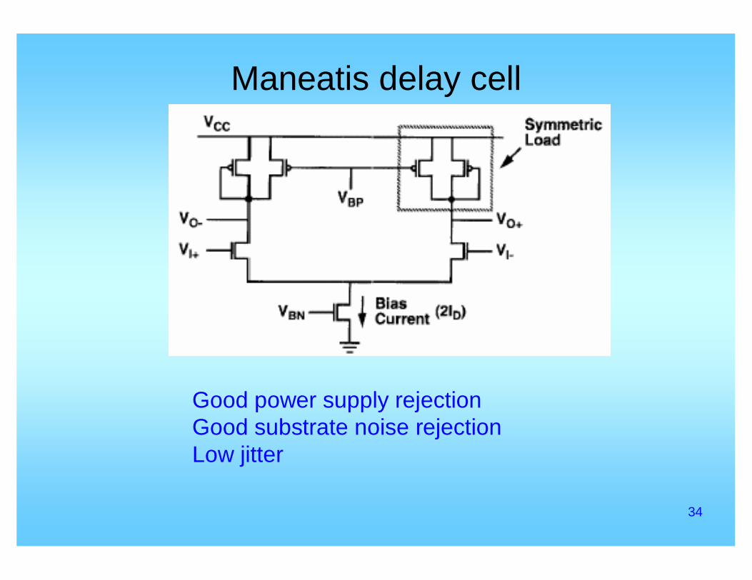
Maneatis delay cell
Good power supply rejectionGood substrate noise rejectionLow jitter
35
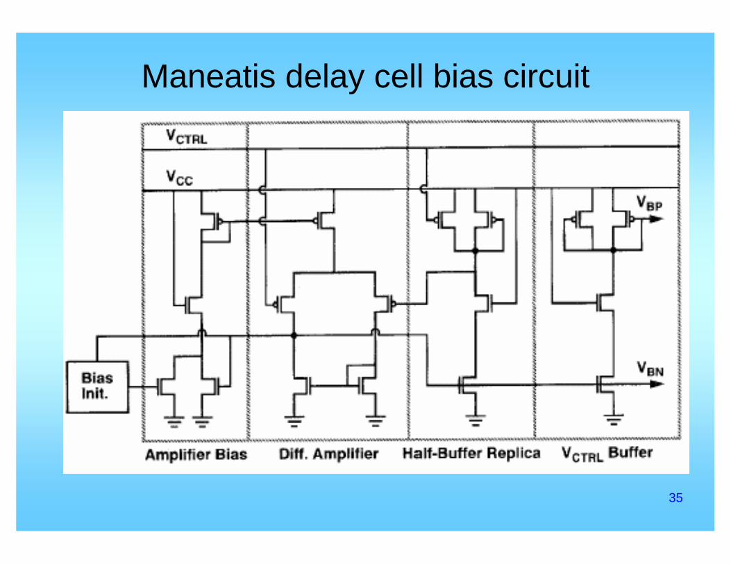
Maneatis delay cell bias circuit
36
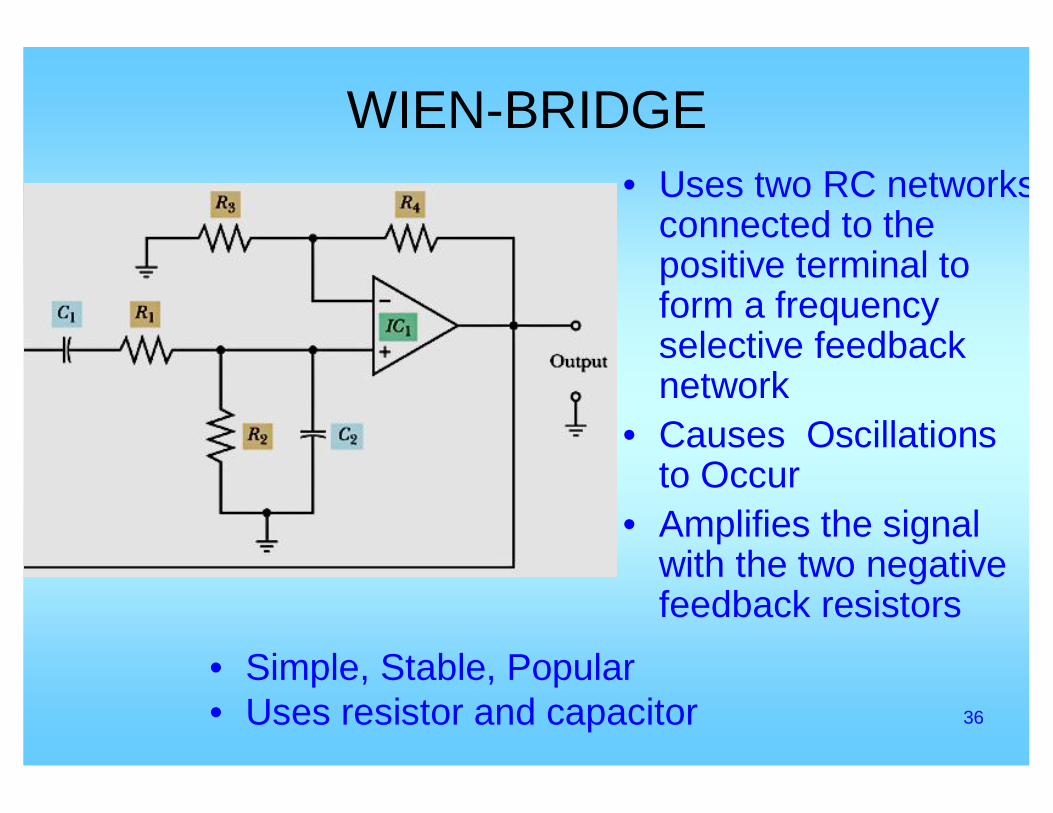
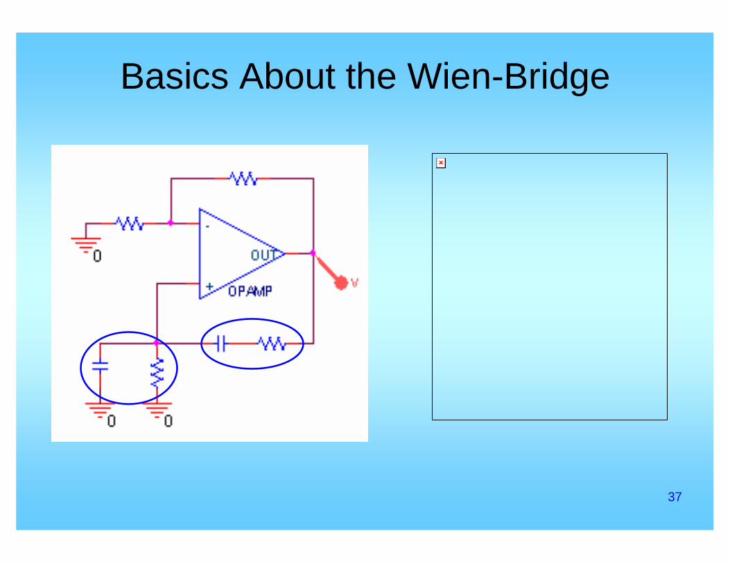
WIEN-BRIDGE
• Simple, Stable, Popular• Uses resistor and capacitor
• Uses two RC networks connected to the positive terminal to form a frequency selective feedback network
• Causes Oscillations to Occur
• Amplifies the signal with the two negative feedback resistors
37
Basics About the Wien-Bridge
38
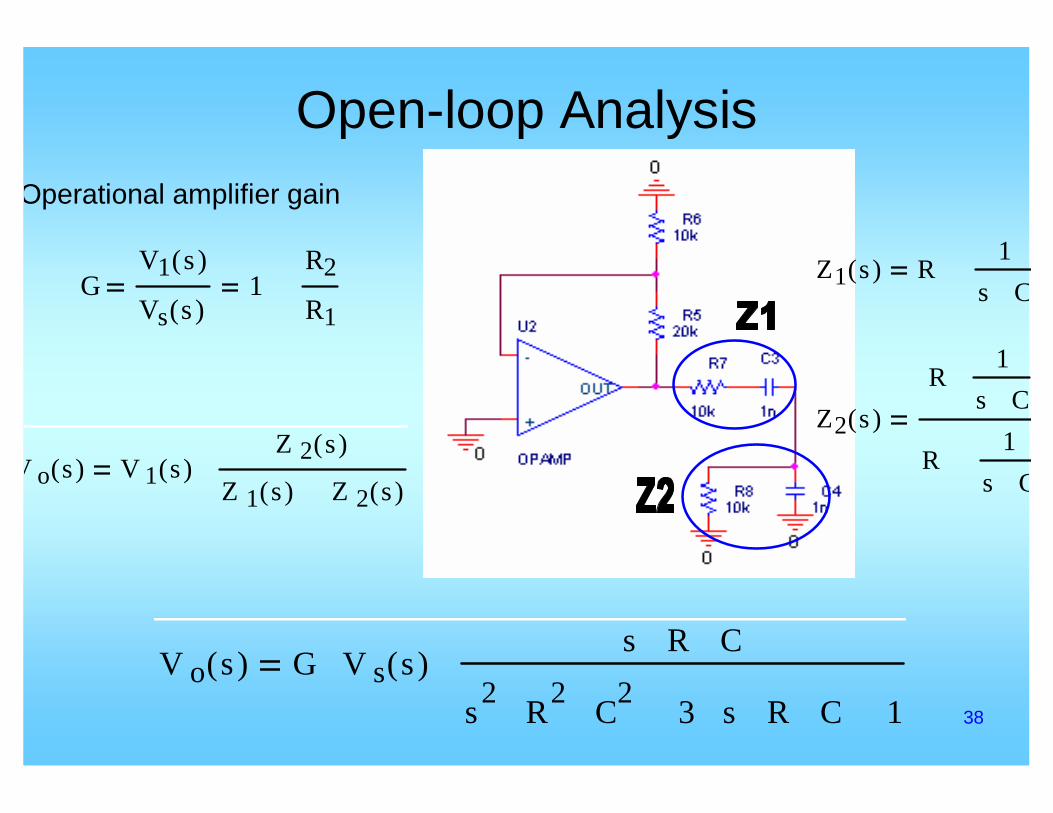
Open-loop Analysis
V o s( ) V 1 s( )Z 2 s( )
Z 1 s( ) Z 2 s( )+⋅
Z1 s( ) R1
s C⋅+
Z2 s( )R
1s C⋅
⋅
R1
s C⋅+
Operational amplifier gain
GV1 s( )
Vs s( )1
R2
R1+
V o s( ) G V s s( )⋅s R⋅ C⋅
s2 R2⋅ C2
⋅ 3 s⋅ R⋅ C⋅+ 1+⋅
39
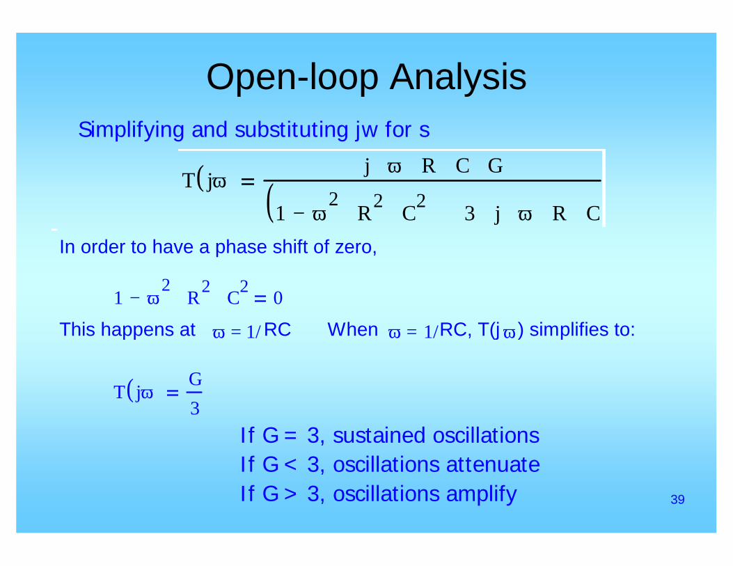
Open-loop Analysis
T jω( ) j ω⋅ R⋅ C⋅ G⋅
1 ω2
R2⋅ C2⋅−( ) 3 j⋅ ω⋅ R⋅ C⋅+
Simplifying and substituting jw for s
In order to have a phase shift of zero,
1 ω2
R2⋅ C2
⋅− 0
This happens at ω = 1/ RC When ω = 1/RC, T(j ω) simplifies to:
T jω( ) G3
If G = 3, sustained oscillationsIf G < 3, oscillations attenuateIf G > 3, oscillations amplify
40
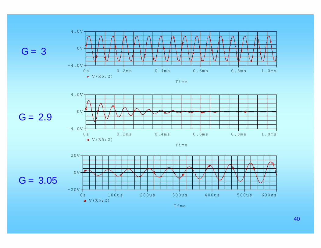
Time
0s 0.2ms 0.4ms 0.6ms 0.8ms 1.0msV(R5:2)
-4.0V
0V
4.0V
G = 3
Time
0s 0.2ms 0.4ms 0.6ms 0.8ms 1.0msV(R5:2)
-4.0V
0V
4.0V
G = 2.9
Time
0s 100us 200us 300us 400us 500us 600usV(R5:2)
-20V
0V
20V
G = 3.05
41
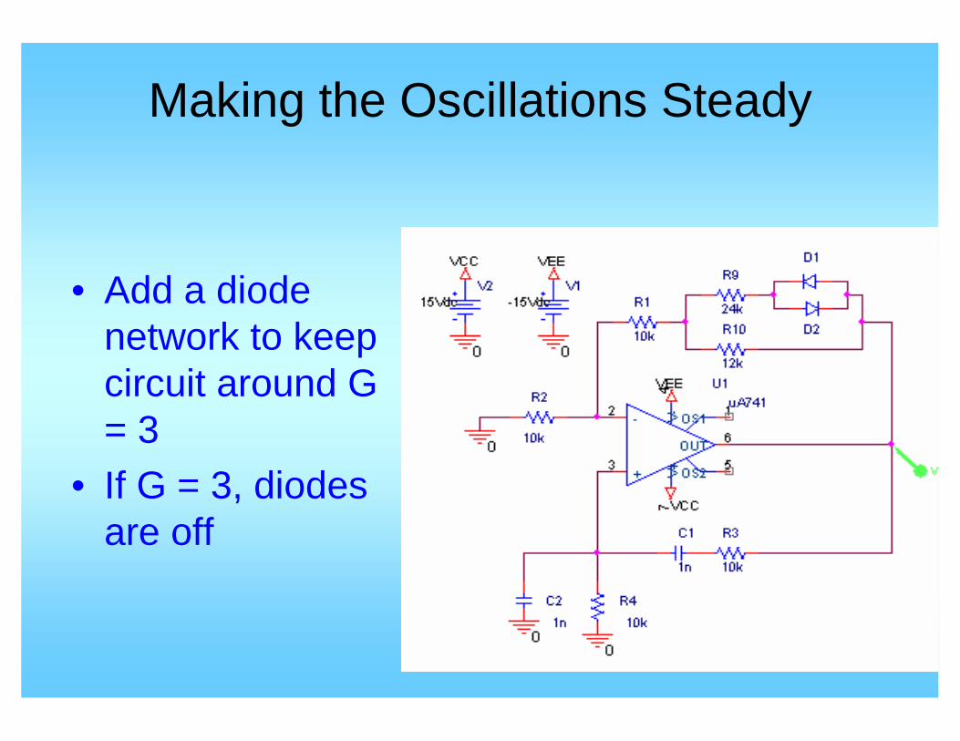
Making the Oscillations Steady
• Add a diode network to keep circuit around G = 3
• If G = 3, diodes are off
42
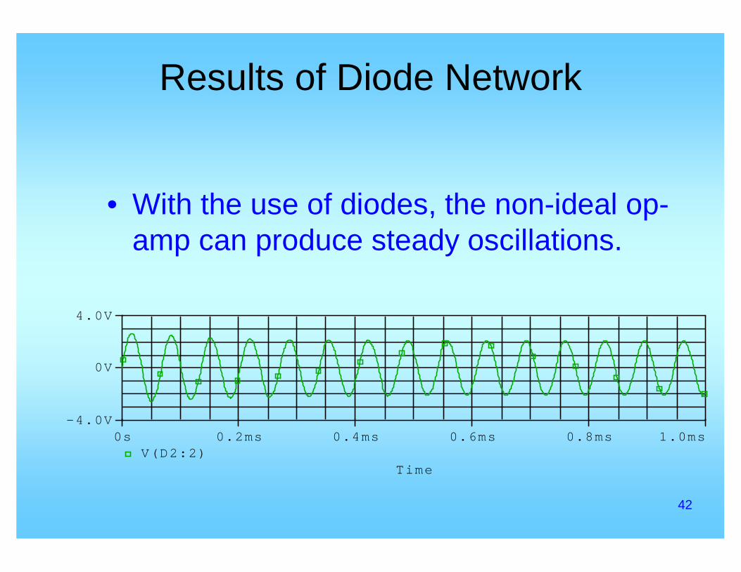
Results of Diode Network
Time
0s 0.2ms 0.4ms 0.6ms 0.8ms 1.0msV(D2:2)
-4.0V
0V
4.0V
• With the use of diodes, the non-ideal op-amp can produce steady oscillations.
43
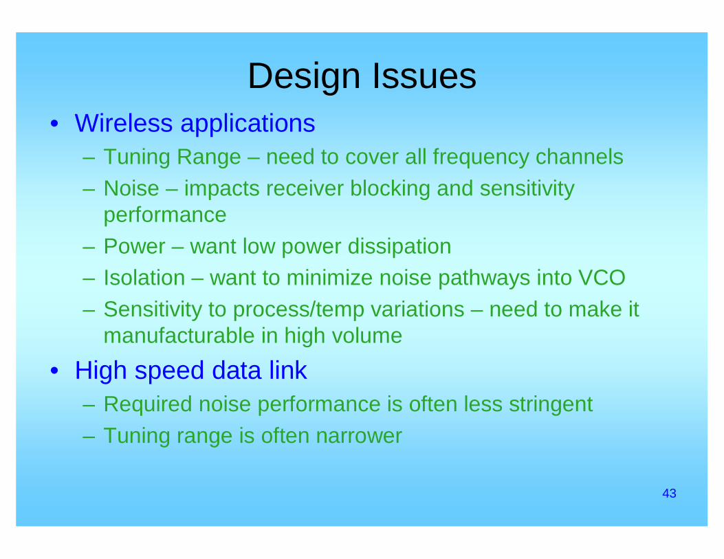
Design Issues• Wireless applications
– Tuning Range – need to cover all frequency channels – Noise – impacts receiver blocking and sensitivity
performance– Power – want low power dissipation– Isolation – want to minimize noise pathways into VCO– Sensitivity to process/temp variations – need to make it
manufacturable in high volume• High speed data link
– Required noise performance is often less stringent– Tuning range is often narrower
44
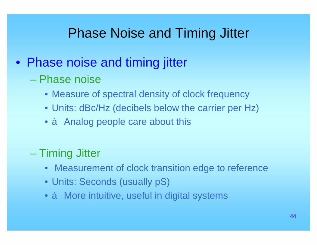
Phase Noise and Timing Jitter
• Phase noise and timing jitter– Phase noise
• Measure of spectral density of clock frequency• Units: dBc/Hz (decibels below the carrier per Hz)• à Analog people care about this
– Timing Jitter• Measurement of clock transition edge to reference• Units: Seconds (usually pS)• à More intuitive, useful in digital systems
45
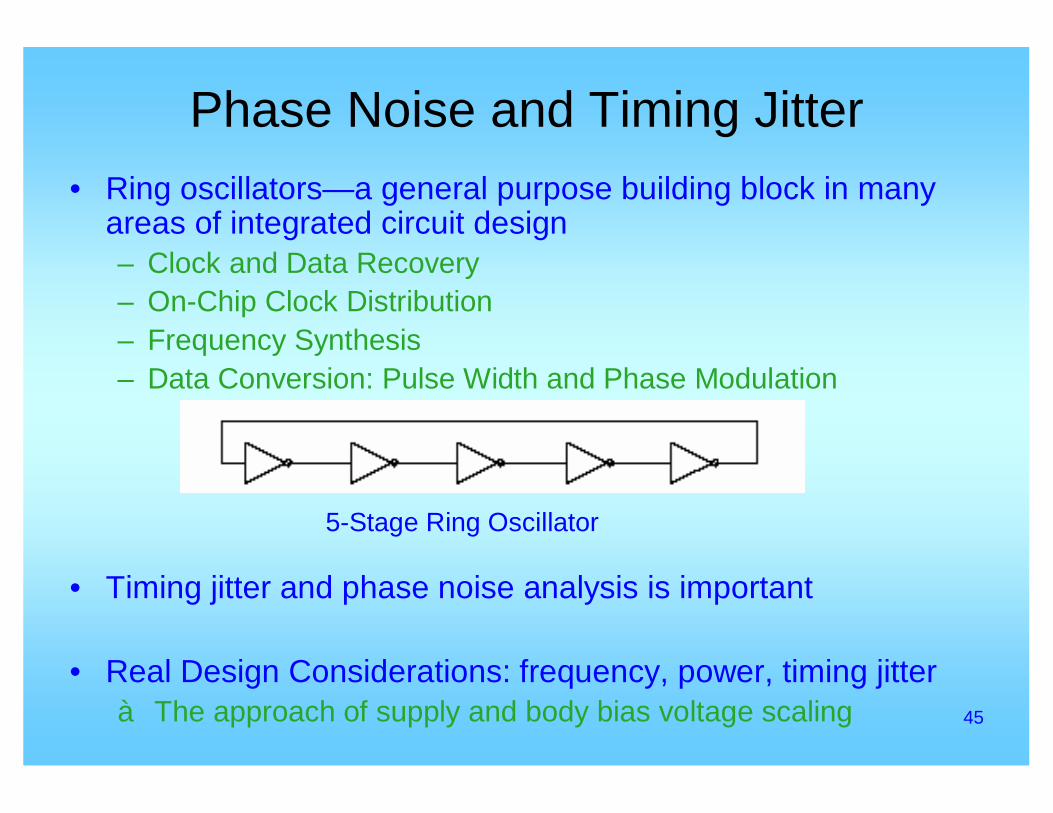
Phase Noise and Timing Jitter• Ring oscillators—a general purpose building block in many
areas of integrated circuit design– Clock and Data Recovery– On-Chip Clock Distribution– Frequency Synthesis– Data Conversion: Pulse Width and Phase Modulation
• Timing jitter and phase noise analysis is important
• Real Design Considerations: frequency, power, timing jitterà The approach of supply and body bias voltage scaling
5-Stage Ring Oscillator
46
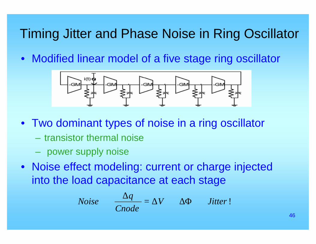
Timing Jitter and Phase Noise in Ring Oscillator
• Modified linear model of a five stage ring oscillator
• Two dominant types of noise in a ring oscillator– transistor thermal noise– power supply noise
• Noise effect modeling: current or charge injected into the load capacitance at each stage
!JitterVCnode
qNoise ⇒∆Φ⇒∆=∆
⇒
47
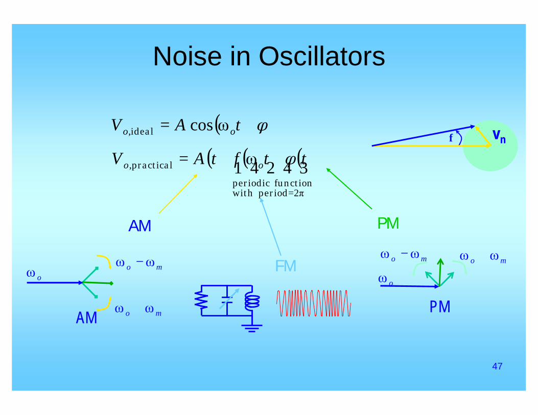
Noise in Oscillators
( )φtAV oo += ωcosideal,
( ) ( )( )43421
π
ω
2period with function periodic
practical,
=
+⋅= tφtftAV oo
AM PM
FM
vnφ
AM
oω
mo ωω +
mo ωω −
PM
mo ωω − mo ωω +
oω
48
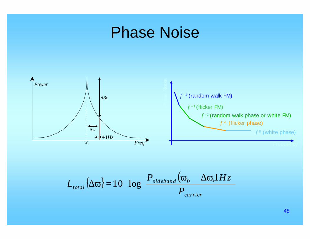
Phase Noise
{ } ( )
ω∆+ω⋅=ω∆
carrier
sidebandtotal P
HzP 1,log10 0L
ω∆
0ωHz1
dBc
Freq
Power
Frequency
Phas
e N
oise
f 0 (white phase)
f -1 (flicker phase)f –2 (random walk phase or white FM)
f –3 (flicker FM)
f –4 (random walk FM)
49
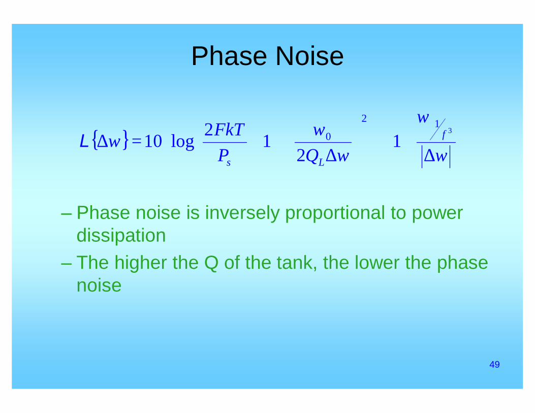
Phase Noise
– Phase noise is inversely proportional to power dissipation
– The higher the Q of the tank, the lower the phase noise
{ }
∆+⋅
∆
+⋅⋅=∆ω
ω
ωω
ω3
12
0 12
12log10 f
Ls QPFkT
L


![The Pythogorean Proposition Diagrams Redrawn [Clean]](https://img.pdfslide.us/doc/110x75/55cf990f550346d0339b51f6/the-pythogorean-proposition-diagrams-redrawn-clean.jpg)