Embed Size (px)
Citation preview
Orion: The Largest Infrared Hybrid Focal Plane in Production
A. Fowler, K.M. Merrill, and W. Ball, NOAO A. Henden and F. Vrba, USNO Flagstaff
C. McCreight, NASA Ames
Abstract Orion is a program to develop a 2048x2048 infrared focal plane using InSb PV detectors. It is the natural follow-on to the successful Aladdin 1024x1024 program, which was the largest IR focal plane of the 90’s. Although the pixels are somewhat smaller than Aladdin, the overall focal plane is over 50mm in size and for the present is the largest IR focal plane of the 21st century. The work is being done by Raytheon Infrared Operations (RIO but better known as SBRC) by many of the same people who created the Aladdin focal plane. The design is very similar to the successful Aladdin design with the addition of reference pixels to lower noise and drift effects in long integrations. So far we have made five focal plane modules with hybridized InSb detectors. In this paper we will discuss the unique design features of this device as well as present test data taken from these devices.
1. Introduction
The Orion program was officially started in the spring of 2001 but informal discussion of the design concept had started earlier. We had our first bare readout for test in late 2001 and to date have made five focal plane modules (FPM). Four of those modules are complete hybrids. Testing has proceeded at both NOAO and RIO on those modules. The University of Rochester group has also been testing the 1Kx1K version of the Orion design. The readout design is solid but some changes are anticipated to improve yield. In addition, more work is needed on the hybrid flatness when it is mounted on the finished module. The Orion design has several features, which have not been previously seen in IR focal planes. The first is 2-adjacent side butt-ability. In fact this has been carried even further on the NGST (Next Generation Space Telescope) focal plane, where 3-side butt-ability is the norm. In addition, we have adopted a packaging scheme that leads directly to 4Kx4K focal plane assemblies. Because of the very high cost of large IR instruments, electronics, and focal planes, we felt 4Kx4K was a prudent design goal at this time. The success of using dead pixels for calibration purposes 1 led us to incorporate several different reference pixel ideas in this design. Recent testing has shown their usefulness in removing the effects of thermal drift from the data. Other improvements are that the focal plane is readout as a single 2Kx2K device rather than in quadrants and it reads out in stripes of 32 columns per output rather than interleaved as has been done in the past. This way you have a dead area rather than missing periodic columns across the whole device. We stuck to the very reliable and proven 2 micron, Pwell, CMOS, single Poly, Double metal process for Orion. With the exception of double metal, this is the same process we used on Aladdin. Double metal was needed because of the long buses (>50mm) in both directions across the readout. This did affect the yield but was required to keep the line impedance low or the speed of readout would have been unacceptable. Orion only has 64 outputs so we needed to maintain the 1.5 µsec per pixel (5t) read time or it would have been severely compromised in the thermal infrared, which is InSb’s strongest point.
2. Design
2.1 Specification
In the preliminary discussions for this program we developed the Orion specifications and goals, which are shown in Table 1.
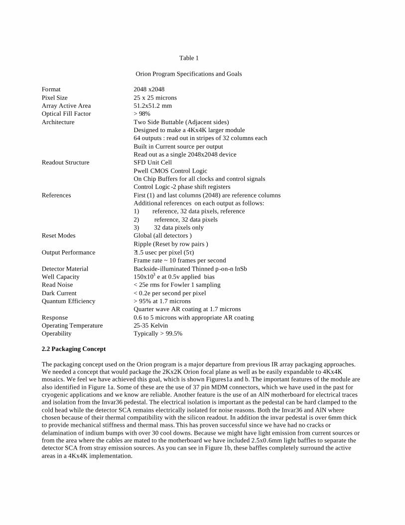
Table 1
Orion Program Specifications and Goals Format 2048 x2048 Pixel Size 25 x 25 microns Array Active Area 51.2x51.2 mm Optical Fill Factor > 98% Architecture Two Side Buttable (Adjacent sides) Designed to make a 4Kx4K larger module 64 outputs : read out in stripes of 32 columns each Built in Current source per output Read out as a single 2048x2048 device Readout Structure SFD Unit Cell Pwell CMOS Control Logic On Chip Buffers for all clocks and control signals Control Logic -2 phase shift registers References First (1) and last columns (2048) are reference columns Additional references on each output as follows: 1) reference, 32 data pixels, reference 2) reference, 32 data pixels 3) 32 data pixels only Reset Modes Global (all detectors ) Ripple (Reset by row pairs ) Output Performance ? 1.5 usec per pixel (5τ) Frame rate ~ 10 frames per second Detector Material Backside-illuminated Thinned p-on-n InSb Well Capacity 150x103 e at 0.5v applied bias Read Noise < 25e rms for Fowler 1 sampling Dark Current < 0.2e per second per pixel Quantum Efficiency > 95% at 1.7 microns Quarter wave AR coating at 1.7 microns Response 0.6 to 5 microns with appropriate AR coating Operating Temperature 25-35 Kelvin Operability Typically > 99.5% 2.2 Packaging Concept
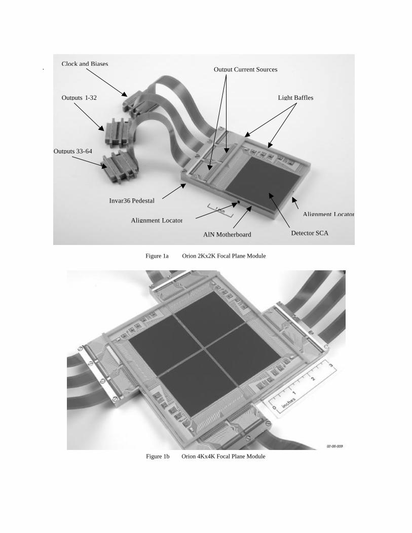
The packaging concept used on the Orion program is a major departure from previous IR array packaging approaches. We needed a concept that would package the 2Kx2K Orion focal plane as well as be easily expandable to 4Kx4K mosaics. We feel we have achieved this goal, which is shown Figures1a and b. The important features of the module are also identified in Figure 1a. Some of these are the use of 37 pin MDM connectors, which we have used in the past for cryogenic applications and we know are reliable. Another feature is the use of an AlN motherboard for electrical traces and isolation from the Invar36 pedestal. The electrical isolation is important as the pedestal can be hard clamped to the cold head while the detector SCA remains electrically isolated for noise reasons. Both the Invar36 and AlN where chosen because of their thermal compatibility with the silicon readout. In addition the invar pedestal is over 6mm thick to provide mechanical stiffness and thermal mass. This has proven successful since we have had no cracks or delamination of indium bumps with over 30 cool downs. Because we might have light emission from current sources or from the area where the cables are mated to the motherboard we have included 2.5x0.6mm light baffles to separate the detector SCA from stray emission sources. As you can see in Figure 1b, these baffles completely surround the active areas in a 4Kx4K implementation.
.
Figure 1a Orion 2Kx2K Focal Plane Module
Figure 1b Orion 4Kx4K Focal Plane Module
Clock and Biases
Outputs 1-32
Outputs 33-64
Invar36 Pedestal
AlN Motherboard Detector SCA
Light Baffles
Output Current Sources
Alignment Locator Alignment Locator
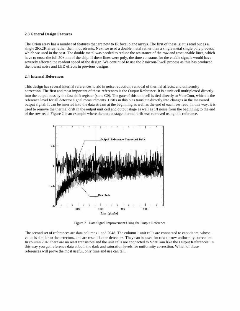
2.3 General Design Features The Orion array has a number of features that are new to IR focal plane arrays. The first of these is; it is read out as a single 2Kx2K array rather than in quadrants. Next we used a double metal rather than a single metal single poly process, which we used in the past. The double metal was needed to reduce the resistance of the row and reset enable lines, which have to cross the full 50+mm of the chip. If these lines were poly, the time constants for the enable signals would have severely affected the readout speed of the design. We continued to use the 2 micron-Pwell process as this has produced the lowest noise and LED effects in previous designs. 2.4 Internal References This design has several internal references to aid in noise reduction, removal of thermal affects, and uniformity correction. The first and most important of these references is the Output Reference. It is a unit cell multiplexed directly into the output buss by the fast shift register (state C0). The gate of this unit cell is tied directly to VdetCom, which is the reference level for all detector signal measurements. Drifts in this bias translate directly into changes in the measured output signal. It can be inserted into the data stream at the beginning as well as the end of each row read. In this way, it is used to remove the thermal drift in the output unit cell and output stage as well as 1/f noise from the beginning to the end of the row read. Figure 2 is an example where the output stage thermal drift was removed using this reference.
Figure 2 Data Signal Improvement Using the Output Reference The second set of references are data columns 1 and 2048. The column 1 unit cells are connected to capacitors, whose value is similar to the detectors, and are reset like the detectors. They can be used for row-to-row uniformity correction. In column 2048 there are no reset transistors and the unit cells are connected to VdetCom like the Output References. In this way you get reference data at both the dark and saturation levels for uniformity correction. Which of these references will prove the most useful, only time and use can tell.
2.5 Output Architecture The Orion output architecture is a departure from past designs in that it is read out in stripes rather than in an interleaved fashion. There are 64 outputs, which is effectively half of the Aladdin device. We needed to maintain the 1.5 µsec/pixel read time or the frame time would have presented great difficulties in the thermal IR. The stripe approach allows us to reduce the output bus capacitance to a minimum, which helps us to achieve the 1.5µsec/pixel read rate. Another feature of the stripe approach is an output failure is confined to a specific area and is not dispersed across the whole array. A secondary result of this approach is the output transistors are distributed across the width (50+mm) of the readout so any emission from those transistors is dispersed across the focal plane and that virtually eliminates any hot spots as seen on other devices.
3. Test Results
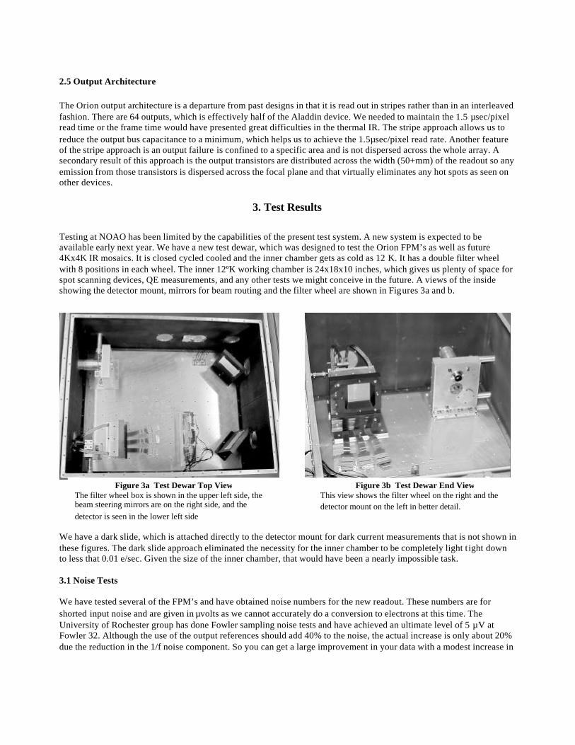
Testing at NOAO has been limited by the capabilities of the present test system. A new system is expected to be available early next year. We have a new test dewar, which was designed to test the Orion FPM’s as well as future 4Kx4K IR mosaics. It is closed cycled cooled and the inner chamber gets as cold as 12 K. It has a double filter wheel with 8 positions in each wheel. The inner 12ºK working chamber is 24x18x10 inches, which gives us plenty of space for spot scanning devices, QE measurements, and any other tests we might conceive in the future. A views of the inside showing the detector mount, mirrors for beam routing and the filter wheel are shown in Figures 3a and b.
We have a dark slide, which is attached directly to the detector mount for dark current measurements that is not shown in these figures. The dark slide approach eliminated the necessity for the inner chamber to be completely light t ight down to less that 0.01 e/sec. Given the size of the inner chamber, that would have been a nearly impossible task. 3.1 Noise Tests We have tested several of the FPM’s and have obtained noise numbers for the new readout. These numbers are for shorted input noise and are given in µvolts as we cannot accurately do a conversion to electrons at this time. The University of Rochester group has done Fowler sampling noise tests and have achieved an ultimate level of 5 µV at Fowler 32. Although the use of the output references should add 40% to the noise, the actual increase is only about 20% due the reduction in the 1/f noise component. So you can get a large improvement in your data with a modest increase in
Figure 3a Test Dewar Top View The filter wheel box is shown in the upper left side, the beam steering mirrors are on the right side, and the detector is seen in the lower left side
Figure 3b Test Dewar End View This view shows the filter wheel on the right and the detector mount on the left in better detail.
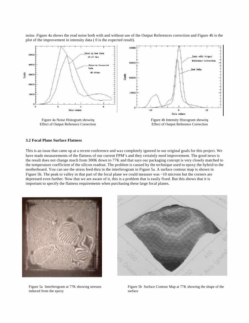
noise. Figure 4a shows the read noise both with and without use of the Output References correction and Figure 4b is the plot of the improvement in intensity data ( 0 is the expected result). 3.2 Focal Plane Surface Flatness This is an issue that came up at a recent conference and was completely ignored in our original goals for this project. We have made measurements of the flatness of our current FPM’s and they certainly need improvement. The good news is the result does not change much from 300K down to 77K and that says our packaging concept is very closely matched to the temperature coefficient of the silicon readout. The problem is caused by the technique used to epoxy the hybrid to the motherboard. You can see the stress feed-thru in the interferogram in Figure 5a. A surface contour map is shown in Figure 5b. The peak to valley in that part of the focal plane we could measure was ~10 microns but the corners are depressed even further. Now that we are aware of it, this is a problem that is easily fixed. But this shows that it is important to specify the flatness requirements when purchasing these large focal planes.
Figure 4a Noise Histogram showing Effect of Output Reference Correction
Figure 4b Intensity Histogram showing Effect of Output Reference Correction
Figure 5a Interferogram at 77K showing stresses induced from the epoxy
Figure 5b Surface Contour Map at 77K showing the shape of the surface

3.3 PED’s In the devices made to date, we have experienced various numbers of PED’s (Photon Emitting Defects). These effects result in the emission of photons, which show up as hot spots (over a large area of the device) in the dark images. This was a problem on Aladdin and a corrective solution was developed at that time. It involves the removal of a small amount (5-10 pixel square area, 0.0025%) of InSb detector material at the defect site. After this has been done, there is no evidence of emission in the surrounding pixels in dark integrations as long as 500 seconds. 3.4 Future Work Much work needs to be done on characterizing these devices. We do not expect any surprises in the area of quantum efficiency as the Orion detectors are being processed and AR coated the same as the Aladdin devices. We have learned some things on the Aladdin program that lead us to believe we may have a solution to the image retention problem but that will have to be proven on future devices. Based on our electrical tests to date, we expect the read noise for Fowler 1 sampling will be in the 20e rms range but we have not proven that yet. So look for more test data and information on performance of these devices in the future.
4. Acknowledgements We want to recognize the extraordinary efforts of the Astronomy Team at RIO. Their work in going from concept to working hardware on the largest infrared focal plane in production is a great achievement. We also wish to acknowledge the financial support of Sidney Wolff of NOAO, NASA, and USNO without which this program wouldn’t have been possible.
5. References 1. G. Finger, H. Mehrgan, M. Meyer, A. Moorwood, G. Nicolini, and J. Stegmeier, “Performance of large-format HgCdTe and InSb arrays for low-background applications, ” Proc. SPIE , Vol. 4008, p. 1280-1297 , Optical and IR Telescope Instrumentation and Detectors, Masanori Iye and Alan Moorwood, Eds., 2000.
![One platform Multiple options...GOST Butt weld DIN Butt weld ANSI Butt weld Socket weld Female 1 pipe thread F-con. ) butt weld GOST Butt weld [mm] [in.] D A SOC FTP F G D A SOC FTP](https://img.pdfslide.us/doc/110x75/5fe23d7adfe1ef18be65fa23/one-platform-multiple-options-gost-butt-weld-din-butt-weld-ansi-butt-weld-socket.jpg)