Embed Size (px)
Citation preview
Institute for Nanostructered Materials CNR, BOLOGNA, ITALY
Organic Semiconductors for Spintronic Applications
V. Alek DEDIU
Italian School of Magnetism, Pavia 2012
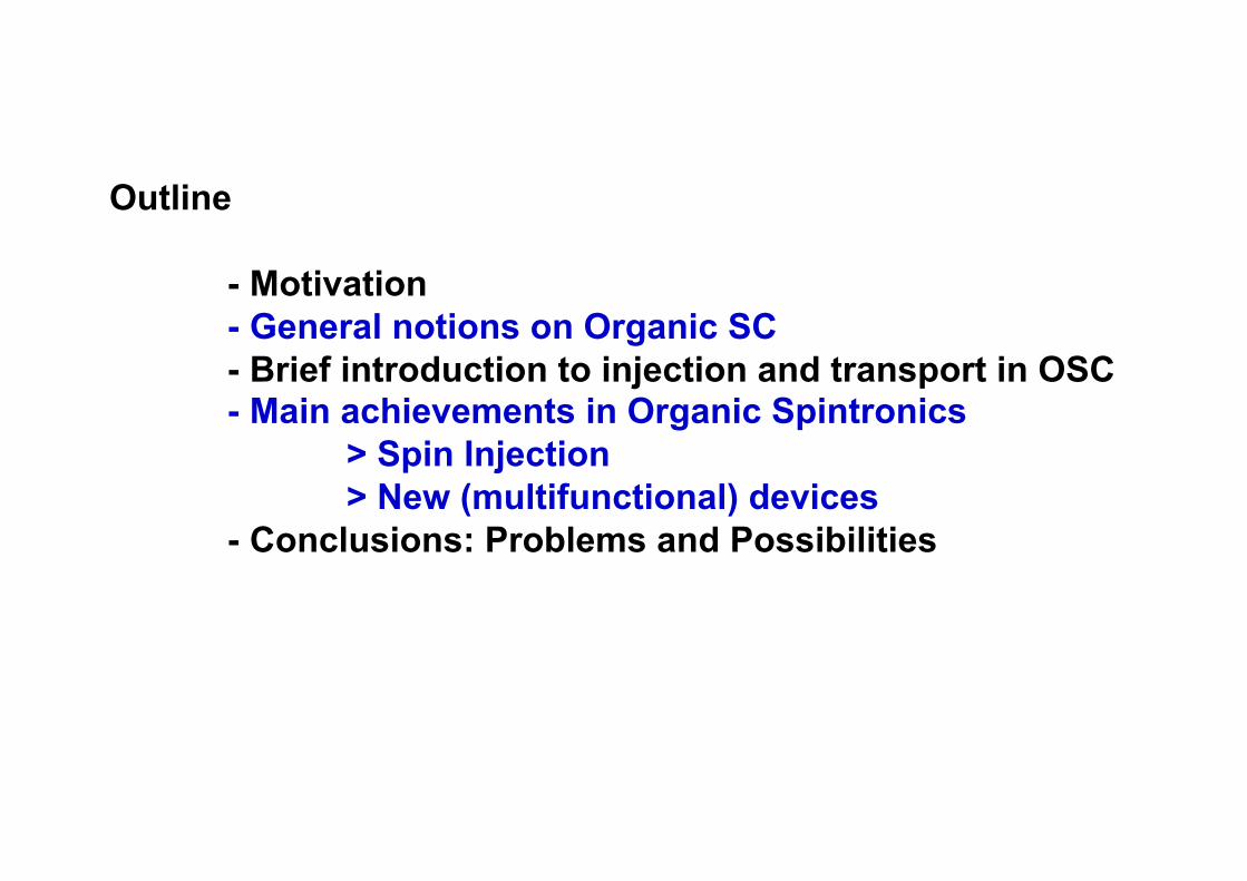
Outline - Motivation - General notions on Organic SC - Brief introduction to injection and transport in OSC - Main achievements in Organic Spintronics > Spin Injection > New (multifunctional) devices - Conclusions: Problems and Possibilities
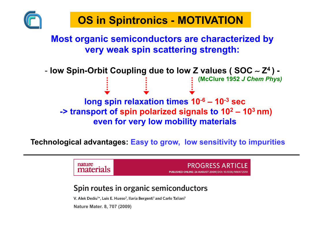
Most organic semiconductors are characterized by very weak spin scattering strength:
- low Spin-Orbit Coupling due to low Z values ( SOC ∼ Z4 ) -
(McClure 1952 J Chem Phys)
OS in Spintronics - MOTIVATION
long spin relaxation times 10-6 – 10-3 sec -> transport of spin polarized signals to 102 – 103 nm)
even for very low mobility materials
Technological advantages: Easy to grow, low sensitivity to impurities
Nature Mater. 8, 707 (2009)
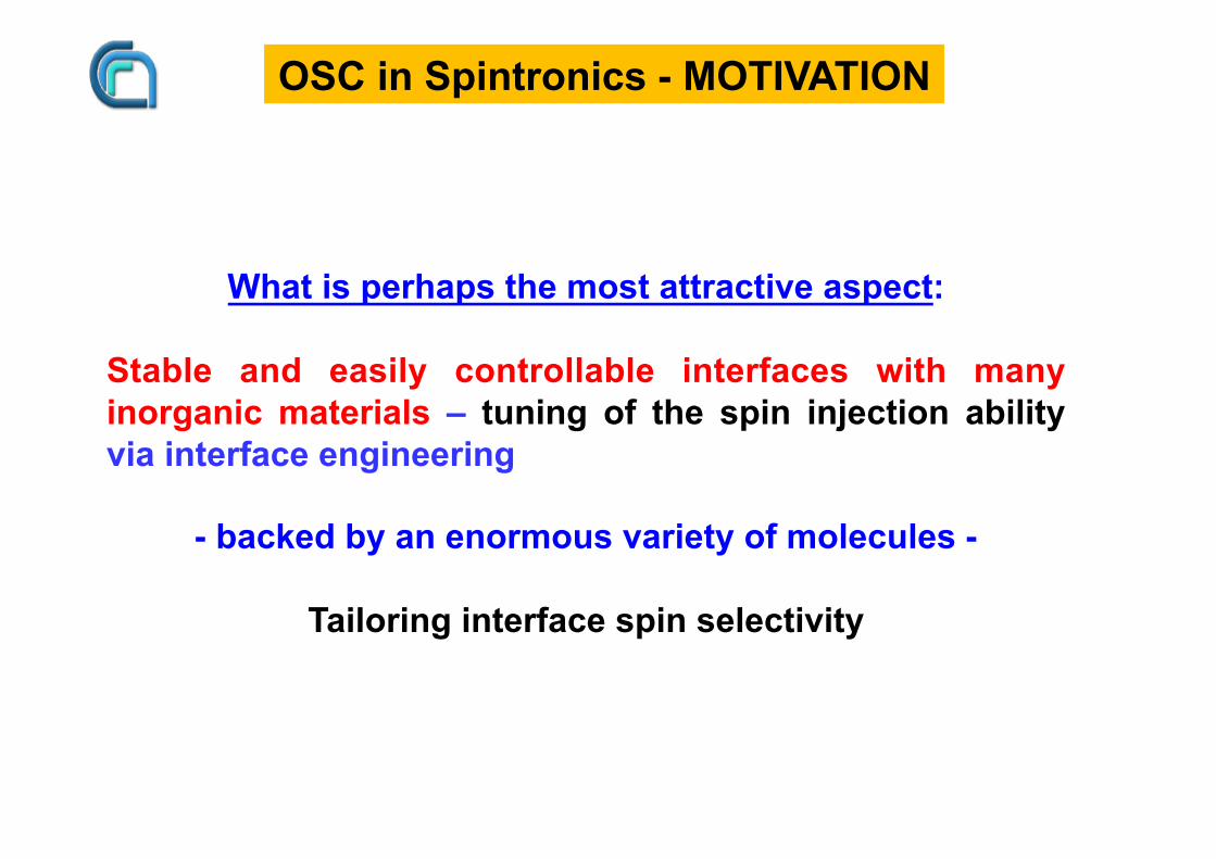
What is perhaps the most attractive aspect:
Stable and easily controllable interfaces with many inorganic materials – tuning of the spin injection ability via interface engineering
- backed by an enormous variety of molecules -
Tailoring interface spin selectivity
OSC in Spintronics - MOTIVATION
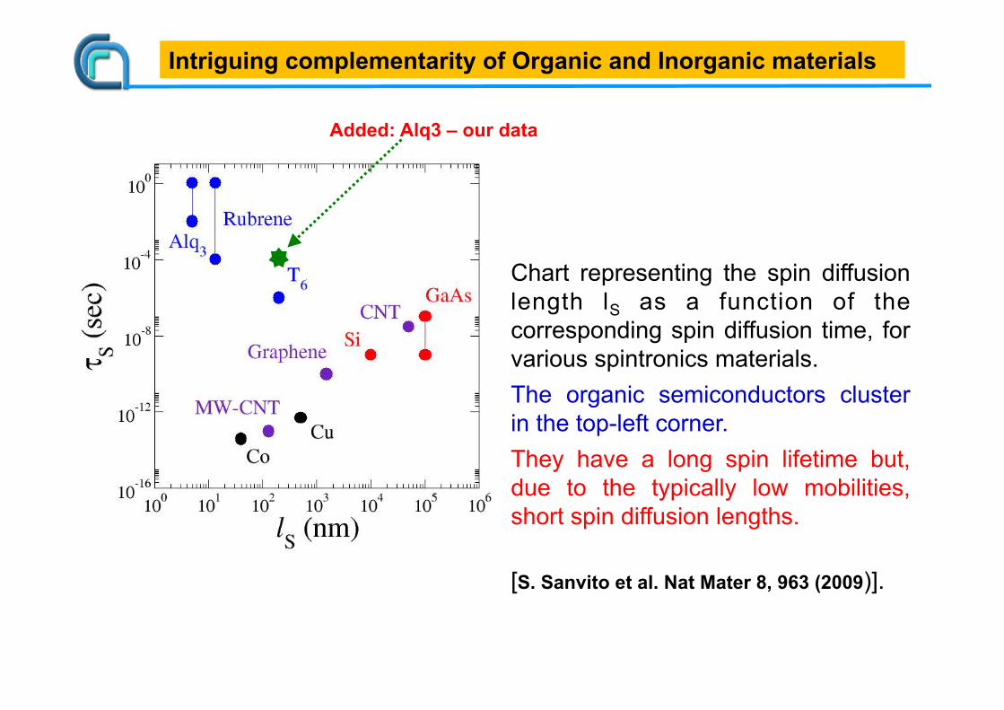
Chart representing the spin diffusion length lS as a function of the corresponding spin diffusion time, for various spintronics materials. The organic semiconductors cluster in the top-left corner. They have a long spin lifetime but, due to the typically low mobilities, short spin diffusion lengths. [S. Sanvito et al. Nat Mater 8, 963 (2009)].
Intriguing complementarity of Organic and Inorganic materials
Added: Alq3 – our data
Flexible PV cell (Konarka)
Organic field-effect transistors
Sony and Samsung 55-inch OLED tv
2010 - Sony Develops a "Rollable“ OTFT-driven OLED Display
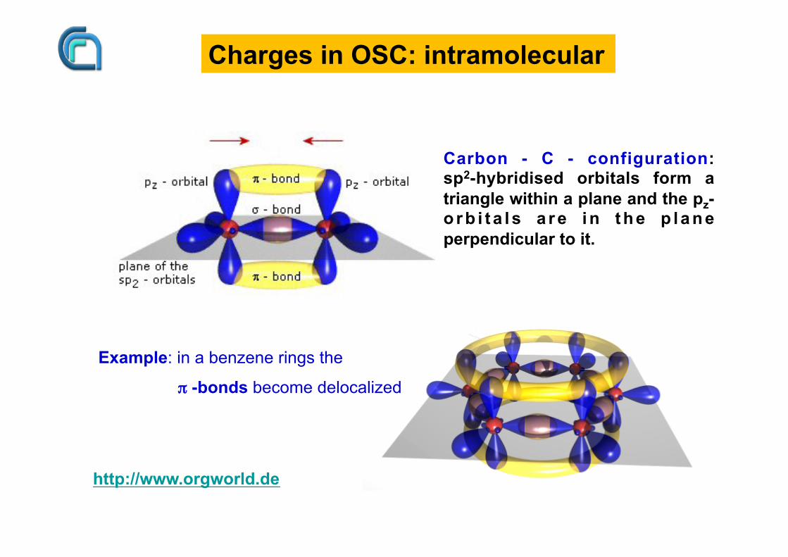
Charges in OSC: intramolecular
Carbon - C - configuration: sp2-hybridised orbitals form a triangle within a plane and the pz-o r b i t a l s a r e i n t h e p l a n e perpendicular to it.
Example: in a benzene rings the
π -bonds become delocalized
http://www.orgworld.de
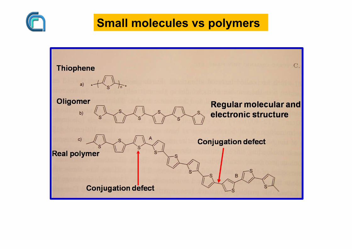
Small molecules vs polymers
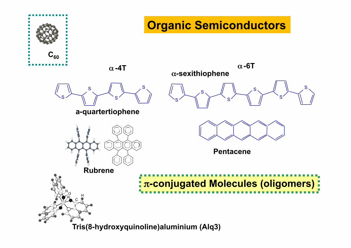
Pentacene
S
S S S
S
S
α -6T
S S
S
S
α -4T
Organic Semiconductors
π-conjugated Molecules (oligomers)
a-quartertiophene
α-sexithiophene
Tris(8-hydroxyquinoline)aluminium (Alq3)
Rubrene
C60
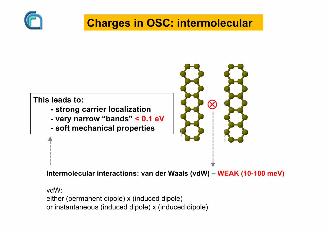
Intermolecular interactions: van der Waals (vdW) – WEAK (10-100 meV) vdW: either (permanent dipole) x (induced dipole) or instantaneous (induced dipole) x (induced dipole)
Charges in OSC: intermolecular
⊗ This leads to: - strong carrier localization - very narrow “bands” < 0.1 eV - soft mechanical properties
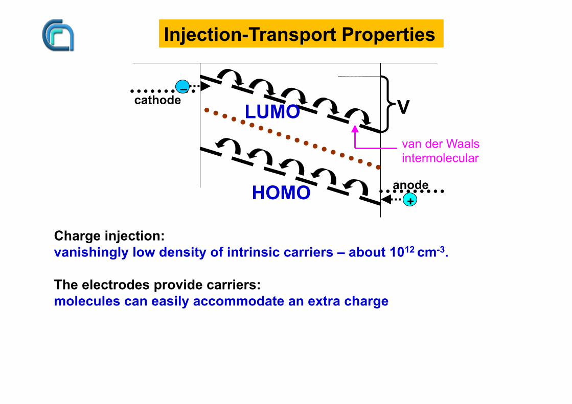
Injection-Transport Properties
Charge injection: vanishingly low density of intrinsic carriers – about 1012 cm-3. The electrodes provide carriers: molecules can easily accommodate an extra charge
_
+
V cathode
anode
LUMO
HOMO
van der Waals intermolecular
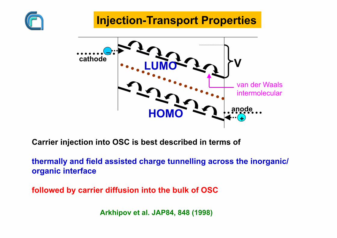
Carrier injection into OSC is best described in terms of thermally and field assisted charge tunnelling across the inorganic/ organic interface followed by carrier diffusion into the bulk of OSC
_
+
V cathode
anode
LUMO
HOMO
van der Waals intermolecular
Arkhipov et al. JAP84, 848 (1998)
Injection-Transport Properties
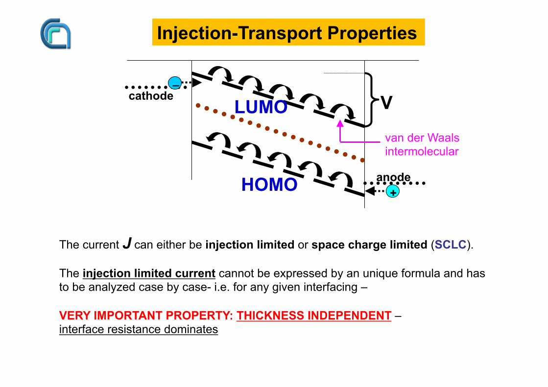
The current J can either be injection limited or space charge limited (SCLC). The injection limited current cannot be expressed by an unique formula and has to be analyzed case by case- i.e. for any given interfacing – VERY IMPORTANT PROPERTY: THICKNESS INDEPENDENT – interface resistance dominates
_
+
V cathode
anode
LUMO
HOMO
van der Waals intermolecular
Injection-Transport Properties
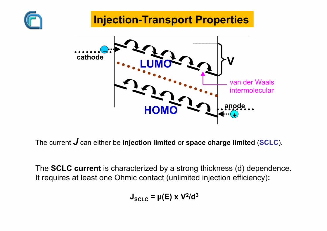
The current J can either be injection limited or space charge limited (SCLC). The SCLC current is characterized by a strong thickness (d) dependence. It requires at least one Ohmic contact (unlimited injection efficiency):
JSCLC = µ(E) x V2/d3
_
+
V cathode
anode
LUMO
HOMO
van der Waals intermolecular
Injection-Transport Properties
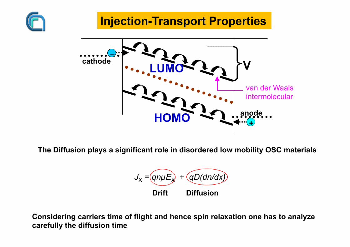
The Diffusion plays a significant role in disordered low mobility OSC materials
JX = qnµEX + qD(dn/dx)
_
+
V cathode
anode
LUMO
HOMO
van der Waals intermolecular
Diffusion Drift
Considering carriers time of flight and hence spin relaxation one has to analyze carefully the diffusion time
Injection-Transport Properties
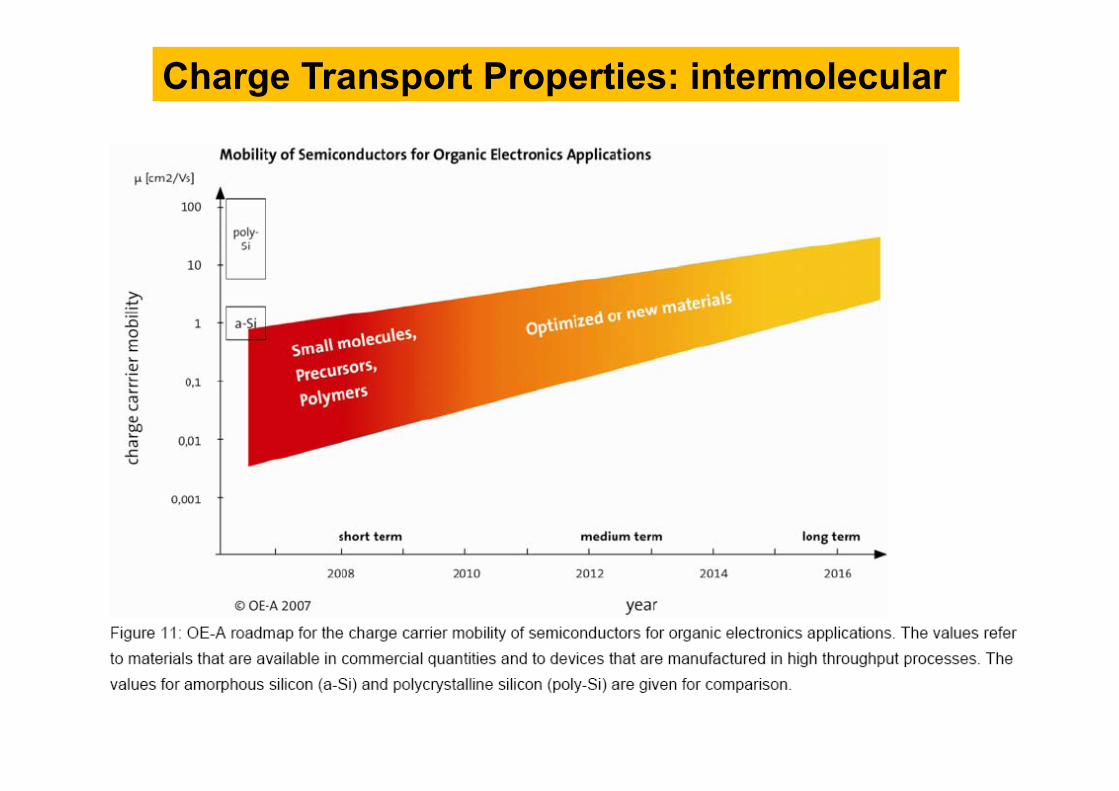
Charge Transport Properties: intermolecular
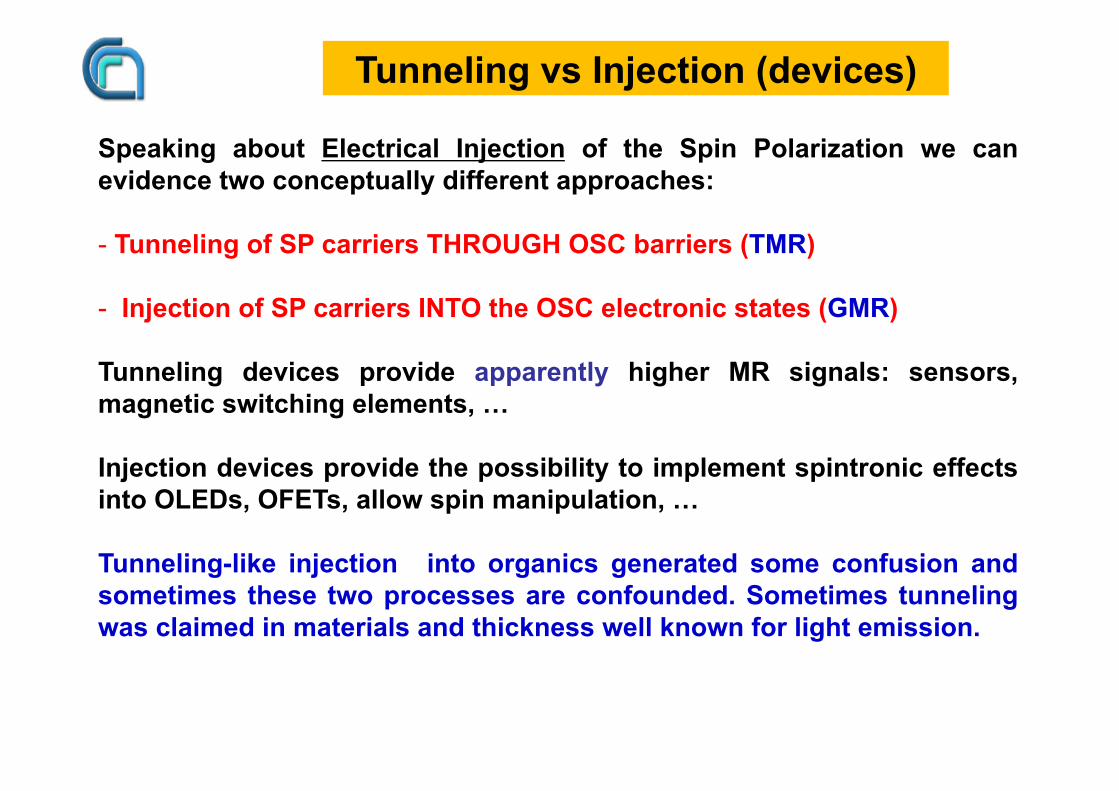
Tunneling vs Injection (devices)
Speaking about Electrical Injection of the Spin Polarization we can evidence two conceptually different approaches: - Tunneling of SP carriers THROUGH OSC barriers (TMR) - Injection of SP carriers INTO the OSC electronic states (GMR) Tunneling devices provide apparently higher MR signals: sensors, magnetic switching elements, … Injection devices provide the possibility to implement spintronic effects into OLEDs, OFETs, allow spin manipulation, … Tunneling-like injection into organics generated some confusion and sometimes these two processes are confounded. Sometimes tunneling was claimed in materials and thickness well known for light emission.
Spin Injection in OSC – where we are? Brief overview
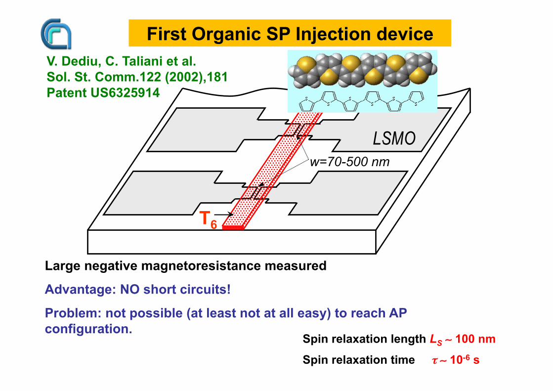
T6
LSMO w=70-500 nm
V. Dediu, C. Taliani et al. Sol. St. Comm.122 (2002),181 Patent US6325914
Large negative magnetoresistance measured
Advantage: NO short circuits!
Problem: not possible (at least not at all easy) to reach AP configuration.
First Organic SP Injection device
Spin relaxation length LS ∼ 100 nm
Spin relaxation time τ ∼ 10-6 s

Z. H. Xiong, V. Vardeny et al. Nature 427, 821 (2004)
Univ. of Utah, Valy Vardeny group:
La0.7Sr0.3MnO3/Alq3(130nm)/Co
Inverse spin valve effect
Demonstration of the Spin Valve effect
The Spin Valve effects were registered in the ±1 V interval, up to 240 K
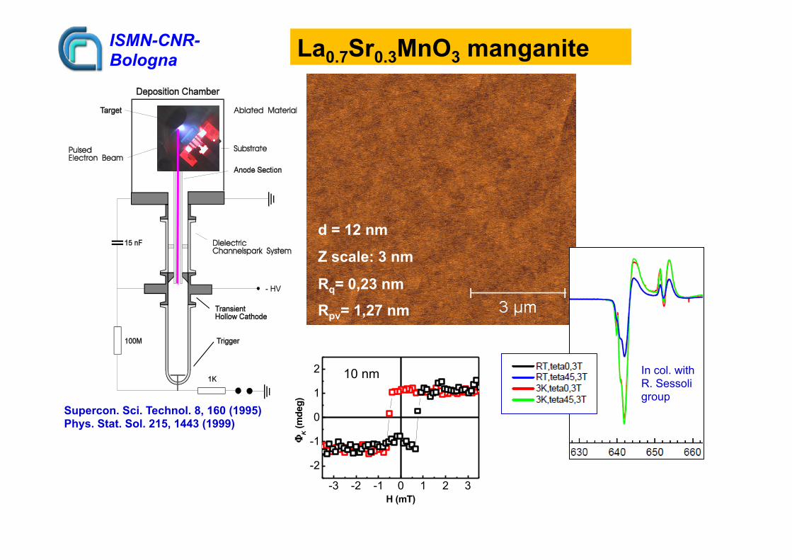
Supercon. Sci. Technol. 8, 160 (1995) Phys. Stat. Sol. 215, 1443 (1999)
La0.7Sr0.3MnO3 manganite
ISMN-CNR-Bologna
d = 12 nm
Z scale: 3 nm
Rq= 0,23 nm
Rpv= 1,27 nm
-3 -2 -1 0 1 2 3
-2
-1
0
1
2 10 nm
ΦK (
mde
g)
H (mT)
In col. with R. Sessoli group
La0.7Sr0.3MnO3/Alq3(130nm)/Co, both electrodes and Alq3, was a lucky choice
It becomes very fast the most used device in organic spintronics in an attempt to understand the physics rather than tsting new materials (or discovering new properties of old ones) Although the second approach becomes also vital and important. It generates new devices (see below)
Further developments
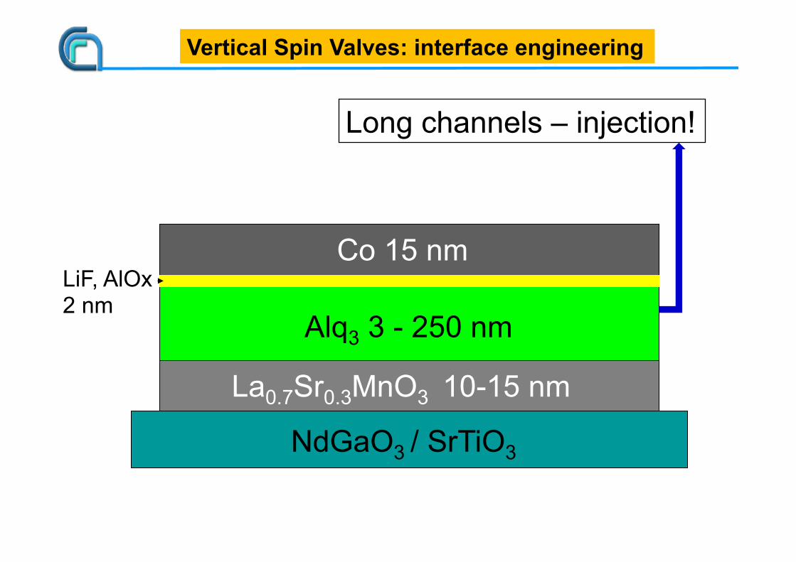
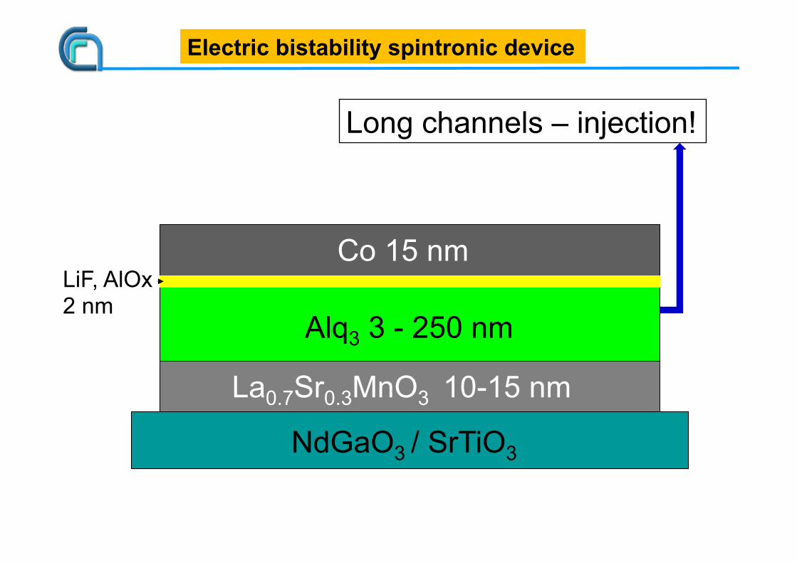
Alq3 3 - 250 nm
Co 15 nm LiF, AlOx 2 nm
Vertical Spin Valves: interface engineering
Long channels – injection!
La0.7Sr0.3MnO3 10-15 nm
NdGaO3 / SrTiO3
PRB78, 115203 (2008)
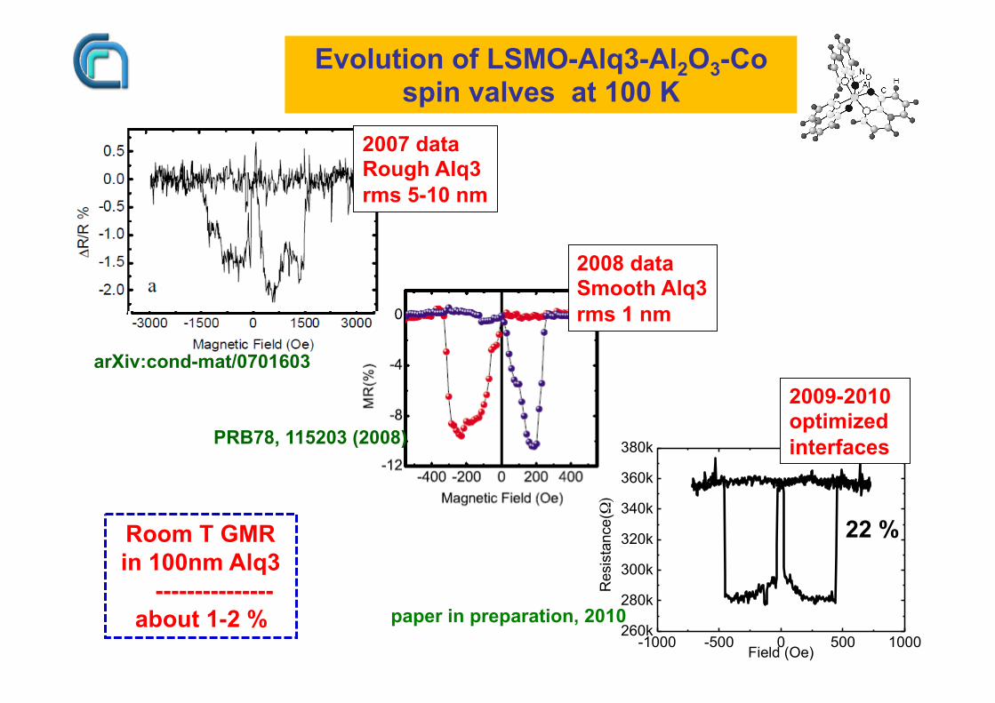
Evolution of LSMO-Alq3-Al2O3-Co spin valves at 100 K
paper in preparation, 2010
22 %
-1000 -500 0 500 1000260k
280k
300k
320k
340k
360k
380k
Res
ista
nce(Ω)
Field (Oe)
2007 data Rough Alq3 rms 5-10 nm
2008 data Smooth Alq3 rms 1 nm
2009-2010 optimized interfaces
arXiv:cond-mat/0701603
Room T GMR in 100nm Alq3 --------------- about 1-2 %
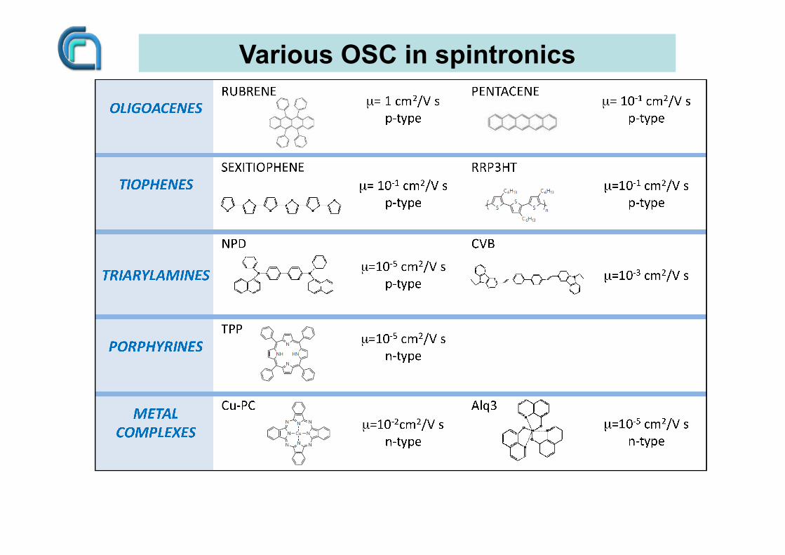
Various OSC in spintronics
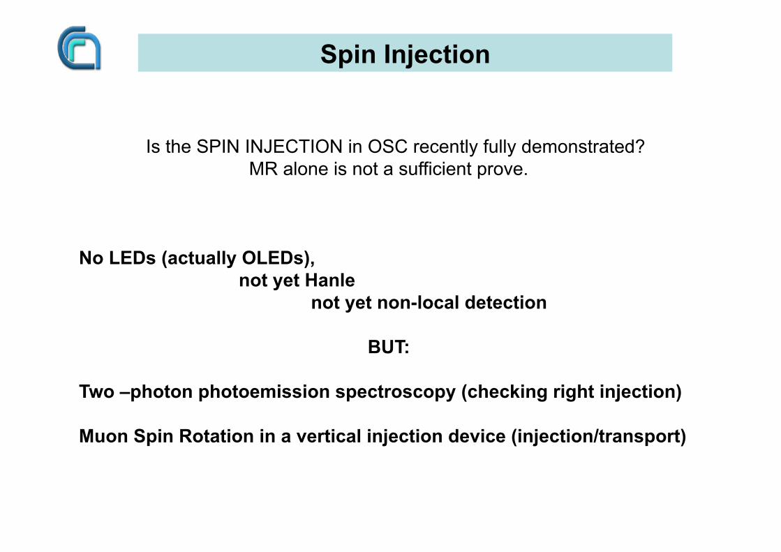
Is the SPIN INJECTION in OSC recently fully demonstrated? MR alone is not a sufficient prove. No LEDs (actually OLEDs), not yet Hanle not yet non-local detection BUT: Two –photon photoemission spectroscopy (checking right injection) Muon Spin Rotation in a vertical injection device (injection/transport)
Spin Injection
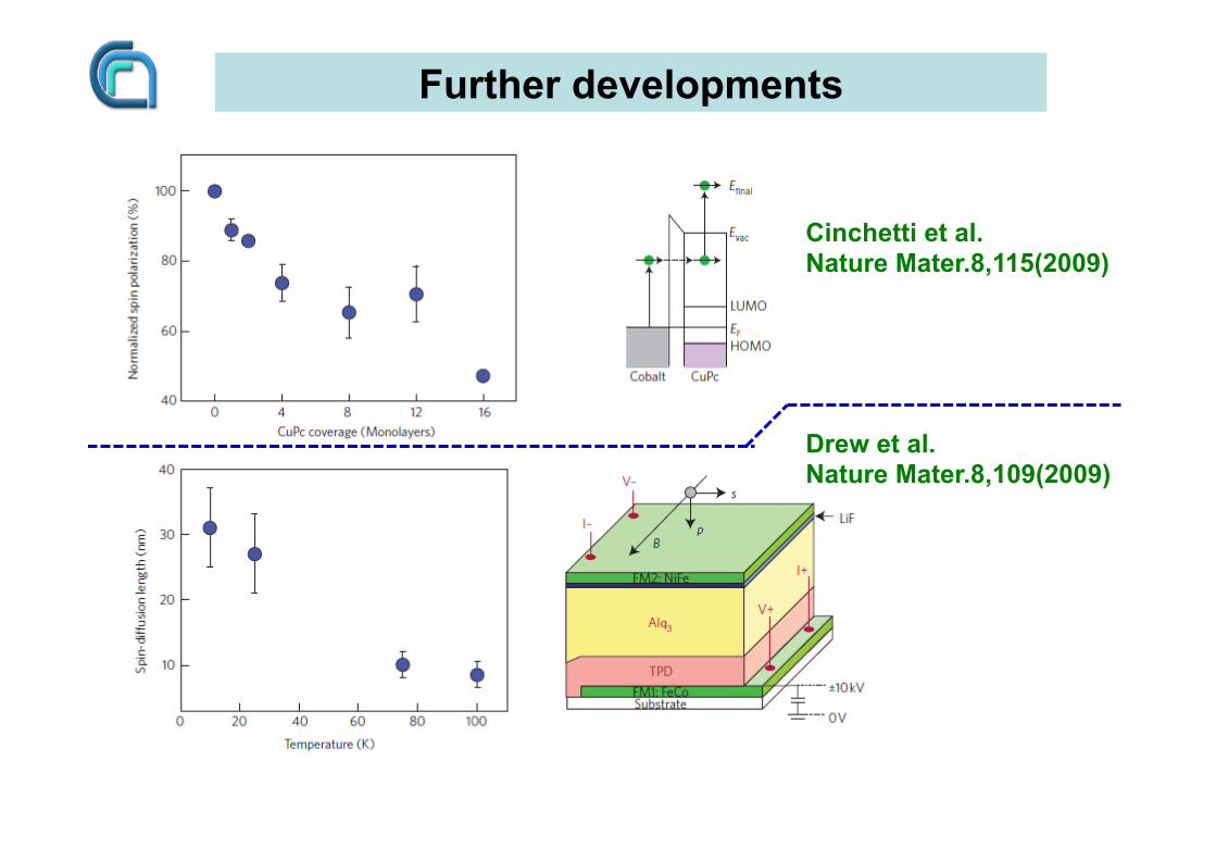
Further developments
Cinchetti et al. Nature Mater.8,115(2009)
Drew et al. Nature Mater.8,109(2009)
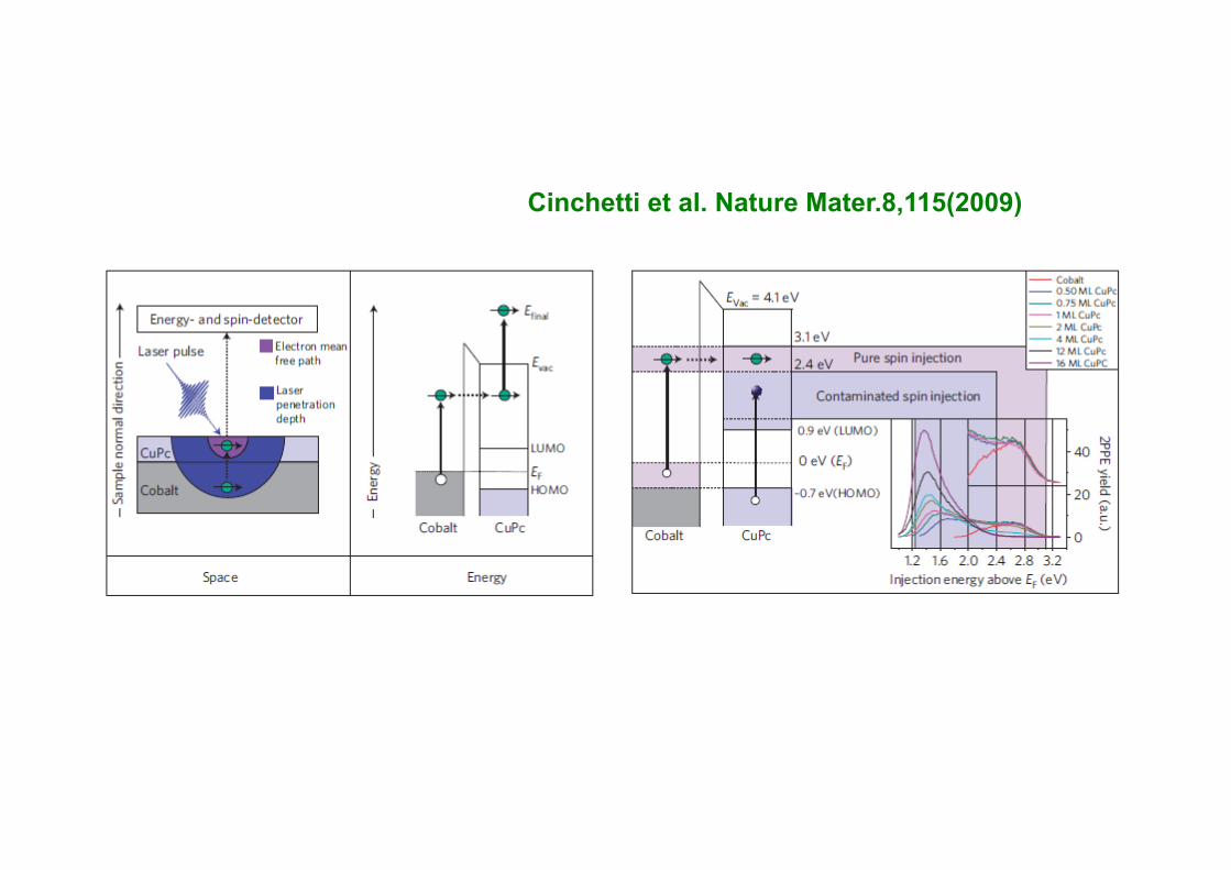
Cinchetti et al. Nature Mater.8,115(2009)
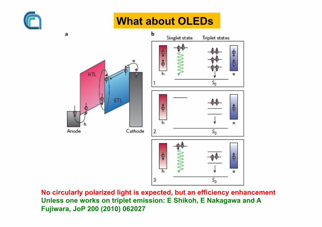
What about OLEDs
No circularly polarized light is expected, but an efficiency enhancement Unless one works on triplet emission: E Shikoh, E Nakagawa and A Fujiwara, JoP 200 (2010) 062027
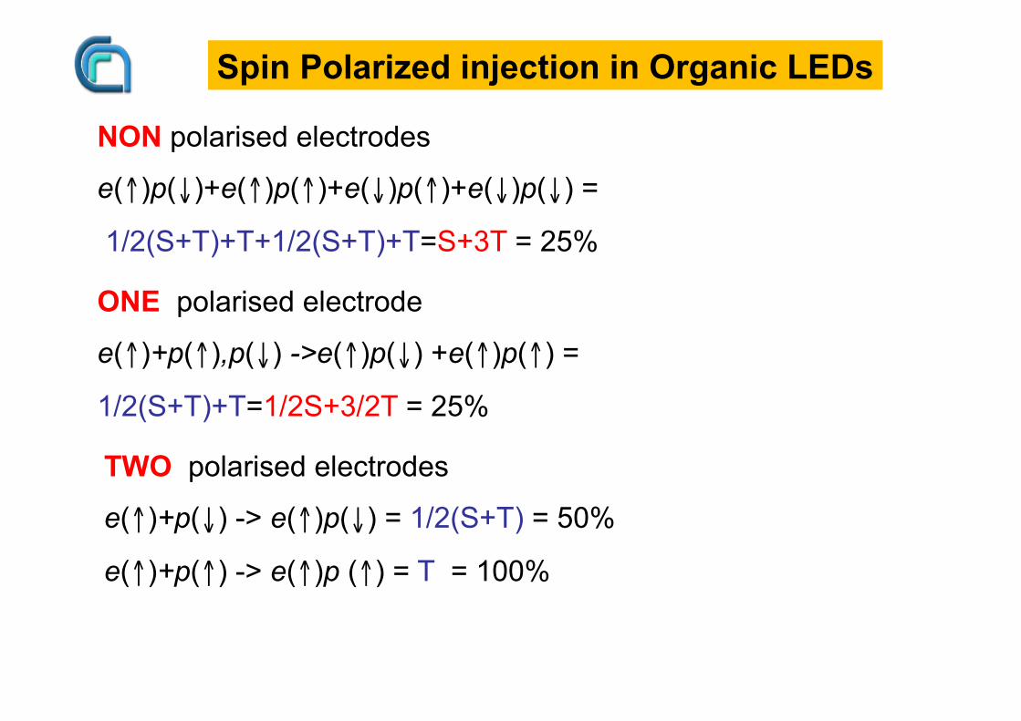
NON polarised electrodes
e(↑)p(↓)+e(↑)p(↑)+e(↓)p(↑)+e(↓)p(↓) =
1/2(S+T)+T+1/2(S+T)+T=S+3T = 25%
ONE polarised electrode
e(↑)+p(↑),p(↓) ->e(↑)p(↓) +e(↑)p(↑) =
1/2(S+T)+T=1/2S+3/2T = 25%
TWO polarised electrodes
e(↑)+p(↓) -> e(↑)p(↓) = 1/2(S+T) = 50%
e(↑)+p(↑) -> e(↑)p (↑) = T = 100%
Spin Polarized injection in Organic LEDs
TPD (70 nm)
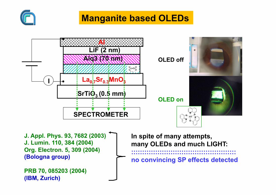
Manganite based OLEDs
OLED off
OLED on
SPECTROMETER
SrTiO3 (0.5 mm)
La0.7Sr0.3MnO3
Alq3 (70 nm)
I
LiF (2 nm) Al
J. Appl. Phys. 93, 7682 (2003) J. Lumin. 110, 384 (2004) Org. Electron. 5, 309 (2004) (Bologna group) PRB 70, 085203 (2004) (IBM, Zurich)
In spite of many attempts, many OLEDs and much LIGHT: :::::::::::::::::::::::::::::::::::::::::::::::: no convincing SP effects detected
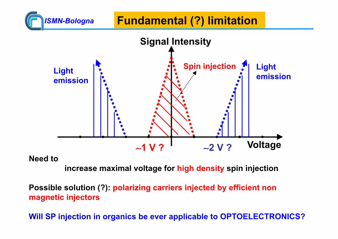
Fundamental (?) limitation
Need to increase maximal voltage for high density spin injection Possible solution (?): polarizing carriers injected by efficient non magnetic injectors Will SP injection in organics be ever applicable to OPTOELECTRONICS?
ISMN-Bologna
Signal Intensity
Voltage
Spin injection Light emission
Light emission
∼1 V ? ∼2 V ?
New Devices from Organic Spintronics

Magnetically Enhanced Memristor (MEM)
What is Memristor?
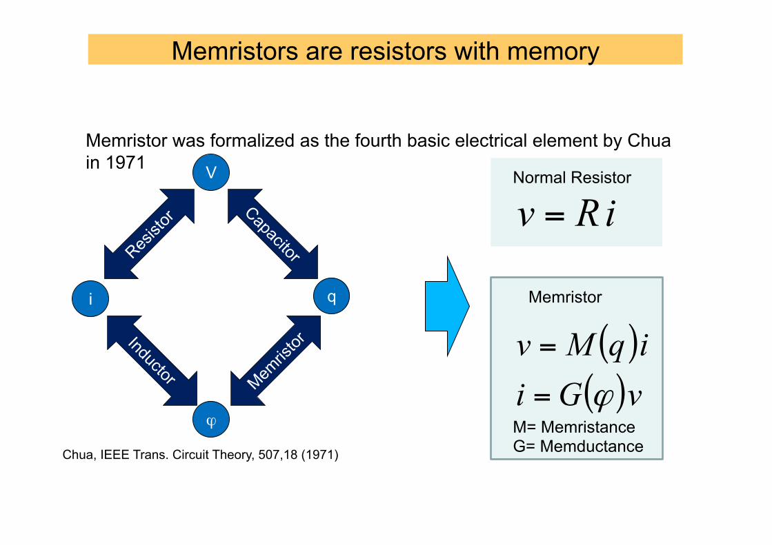
Memristors are resistors with memory
Memristor was formalized as the fourth basic electrical element by Chua in 1971
Chua, IEEE Trans. Circuit Theory, 507,18 (1971)
V
q i
ϕ
iRv =Normal Resistor
( )( )vGi
iqMvϕ=
=
Memristor
M= Memristance G= Memductance
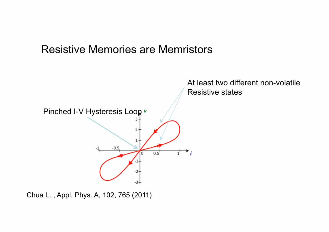
Resistive Memories are Memristors
Pinched I-V Hysteresis Loop
At least two different non-volatile Resistive states
Chua L. , Appl. Phys. A, 102, 765 (2011)
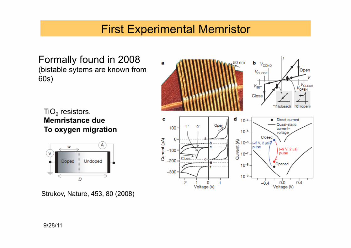
First Experimental Memristor
9/28/11
Strukov, Nature, 453, 80 (2008)
Formally found in 2008 (bistable sytems are known from 60s)
TiO2 resistors. Memristance due To oxygen migration
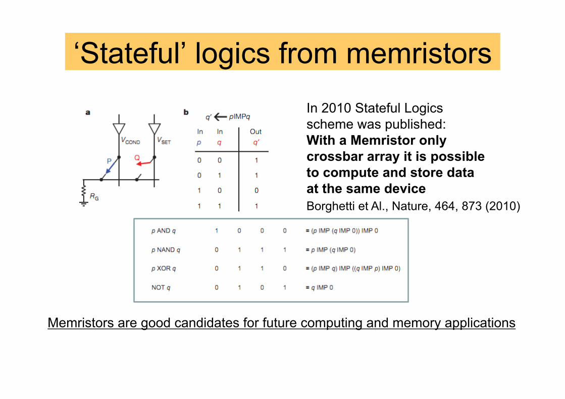
‘Stateful’ logics from memristors
In 2010 Stateful Logics scheme was published: With a Memristor only crossbar array it is possible to compute and store data at the same device
Memristors are good candidates for future computing and memory applications
Borghetti et Al., Nature, 464, 873 (2010)
Alq3 3 - 250 nm
Co 15 nm LiF, AlOx 2 nm
Electric bistability spintronic device
Long channels – injection!
La0.7Sr0.3MnO3 10-15 nm
NdGaO3 / SrTiO3
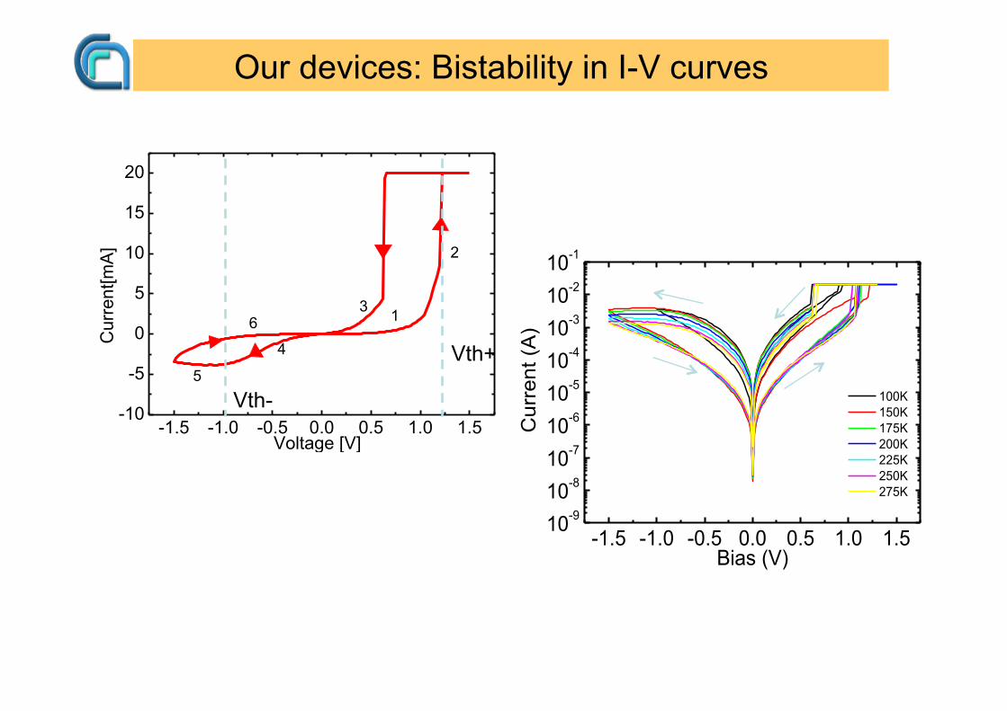
Our devices: Bistability in I-V curves
-1.5 -1.0 -0.5 0.0 0.5 1.0 1.510-910-810-710-610-510-410-310-210-1
100K 150K 175K 200K 225K 250K 275K
Cur
rent
(A)
Bias (V)
-1.5 -1.0 -0.5 0.0 0.5 1.0 1.5-10
-5
0
5
10
15
20
Cur
rent
[mA
]
Voltage [V]
1
2
3
4
5
6
Vth+
Vth-
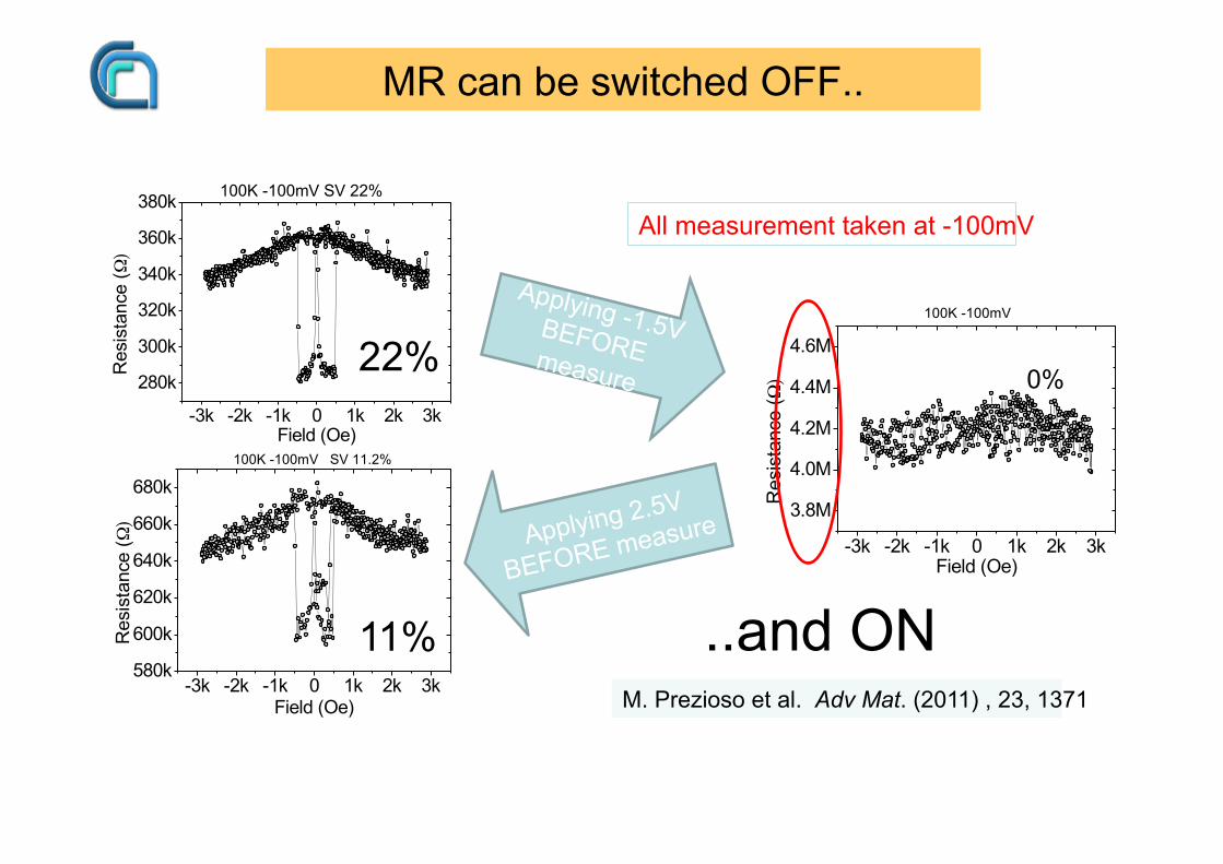
MR can be switched OFF..
-3k -2k -1k 0 1k 2k 3k
3.8M
4.0M
4.2M
4.4M
4.6M
Res
ista
nce
(Ω)
Field (Oe)
100K -100mV
-3k -2k -1k 0 1k 2k 3k
280k
300k
320k
340k
360k
380k
Res
ista
nce
(Ω)
Field (Oe)
100K -100mV SV 22%
0%
..and ON -3k -2k -1k 0 1k 2k 3k
580k
600k
620k
640k
660k
680k
Res
ista
nce
(Ω)
Field (Oe)
100K -100mV SV 11.2%
Applying 2.5V
BEFORE measure
All measurement taken at -100mV
11%
22%
M. Prezioso et al. Adv Mat. (2011) , 23, 1371
Applying -1.5V BEFORE measure
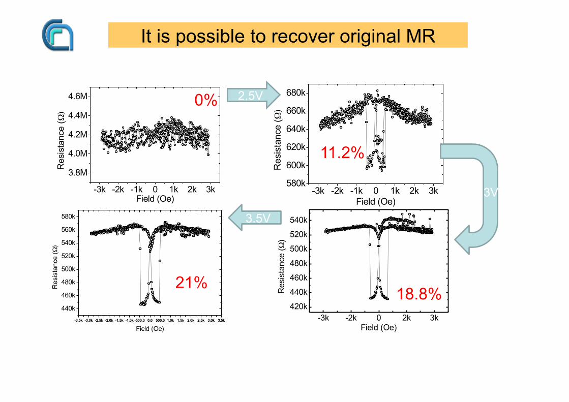
It is possible to recover original MR
-3k -2k -1k 0 1k 2k 3k580k
600k
620k
640k
660k
680k
Res
ista
nce
(Ω)
Field (Oe)
-3.5k -3.0k -2.5k -2.0k -1.5k -1.0k -500.0 0.0 500.0 1.0k 1.5k 2.0k 2.5k 3.0k 3.5k
440k
460k
480k
500k
520k
540k
560k
580k
Res
ista
nce
(Ω)
Field (Oe)
2.5V
3.5V
3V
0%
11.2%
18.8% 21%
-3k -2k -1k 0 1k 2k 3k
3.8M
4.0M
4.2M
4.4M
4.6M
Res
ista
nce
(Ω)
Field (Oe)
-3k -2k 0 2k 3k420k
440k
460k
480k
500k
520k
540k
Res
ista
nce
(Ω)
Field (Oe)
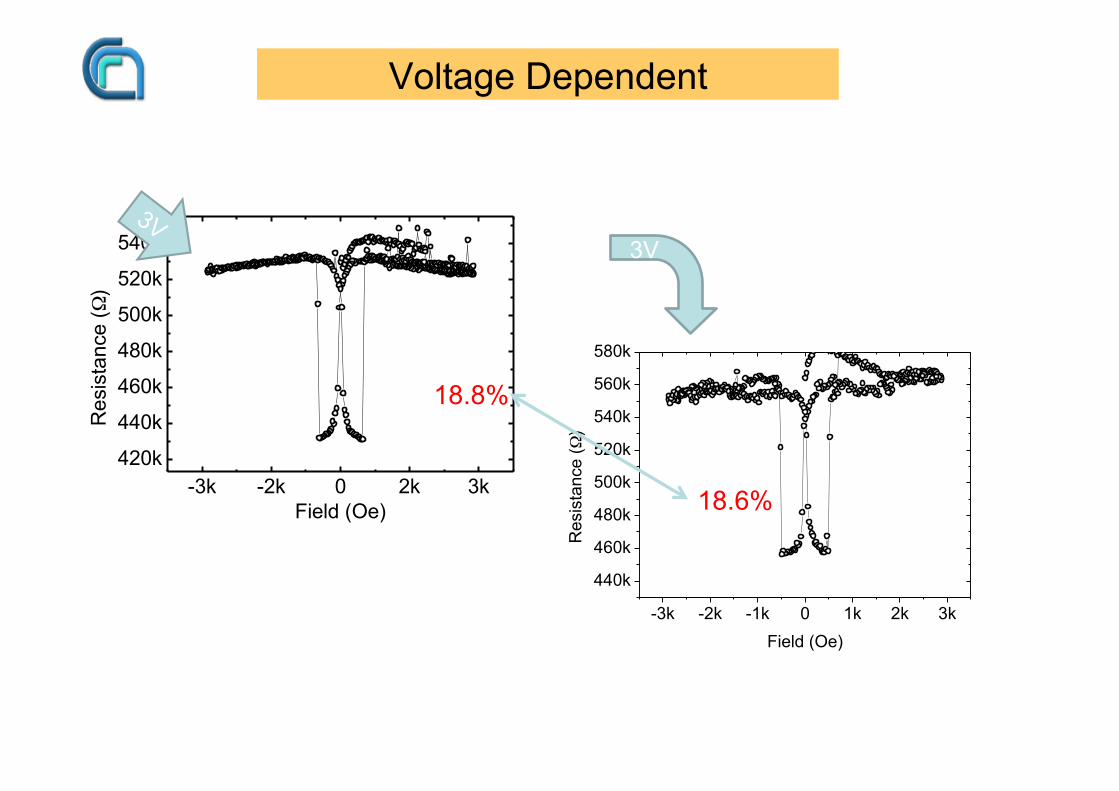
Voltage Dependent
-3k -2k -1k 0 1k 2k 3k
440k
460k
480k
500k
520k
540k
560k
580k
Res
ista
nce
(Ω)
Field (Oe)
-3k -2k 0 2k 3k420k
440k
460k
480k
500k
520k
540k
Res
ista
nce
(Ω)
Field (Oe)
3V
18.8%
18.6%
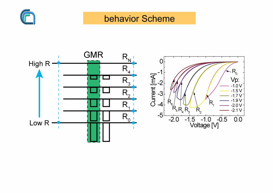
behavior Scheme
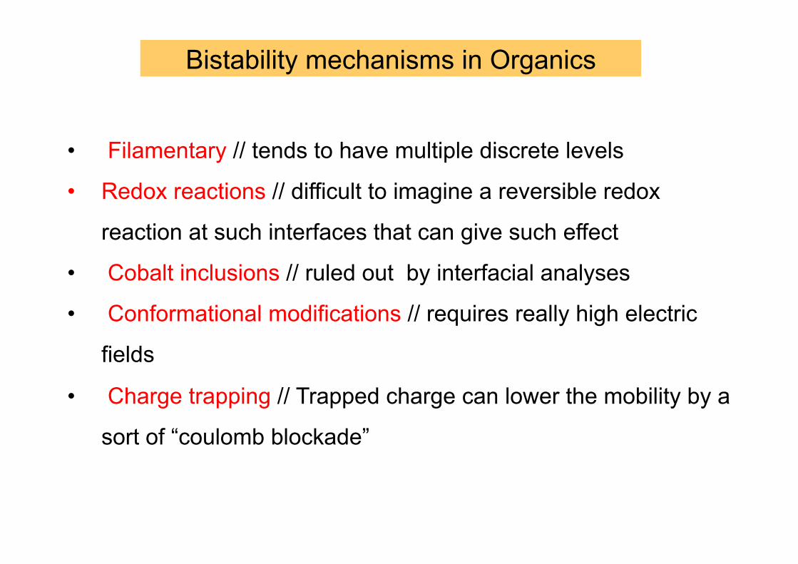
Bistability mechanisms in Organics
• Filamentary // tends to have multiple discrete levels
• Redox reactions // difficult to imagine a reversible redox
reaction at such interfaces that can give such effect
• Cobalt inclusions // ruled out by interfacial analyses
• Conformational modifications // requires really high electric
fields
• Charge trapping // Trapped charge can lower the mobility by a
sort of “coulomb blockade”
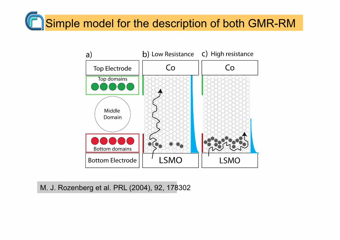
Simple model for the description of both GMR-RM
M. J. Rozenberg et al. PRL (2004), 92, 178302
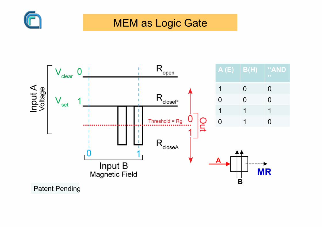
MEM as Logic Gate
A (E) B(H) “AND”
1 0 0 0 0 0 1 1 1 0 1 0
A
B MR
Patent Pending
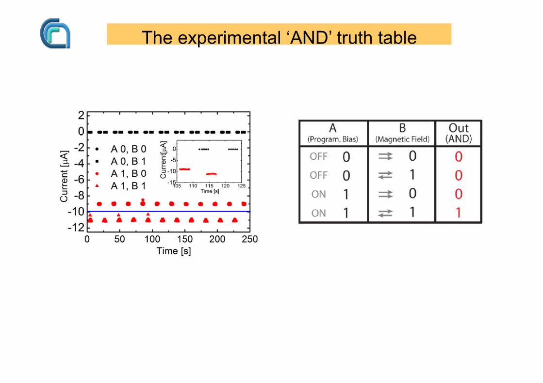
The experimental ‘AND’ truth table
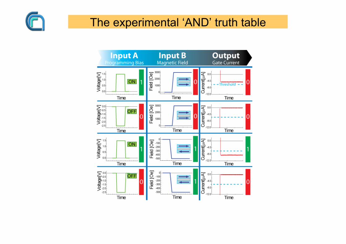
The experimental ‘AND’ truth table
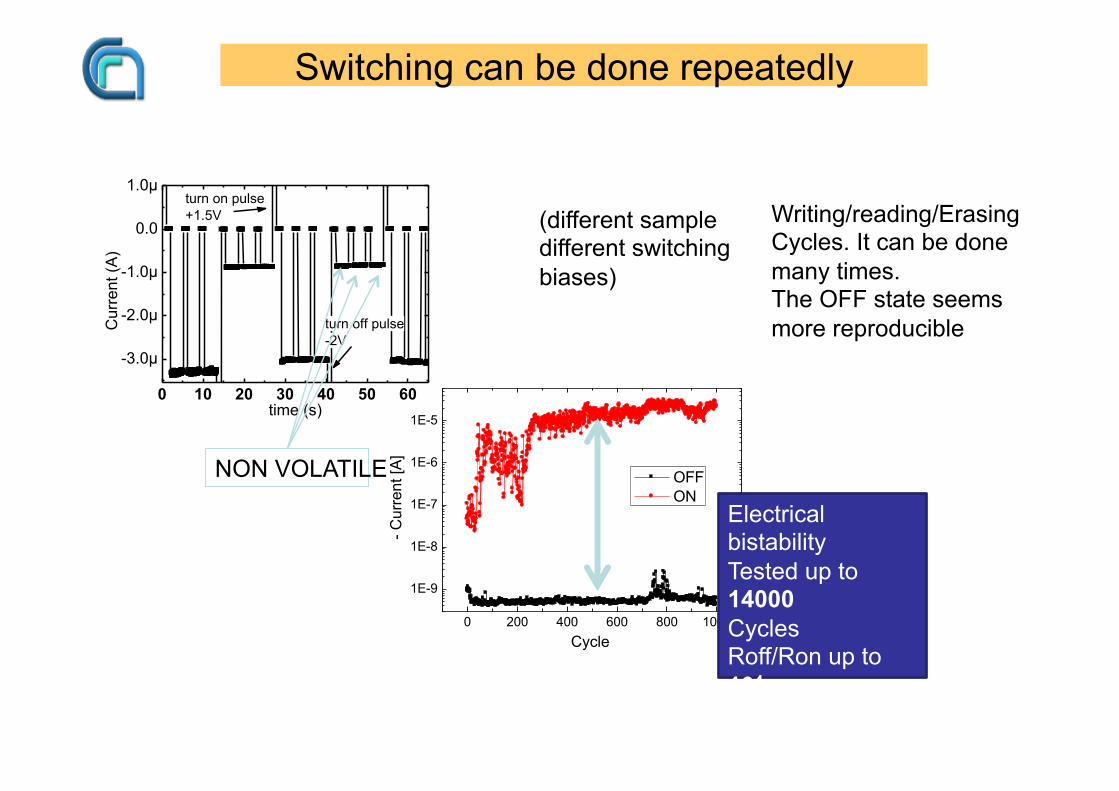
Switching can be done repeatedly
0 10 20 30 40 50 60
-3.0µ
-2.0µ
-1.0µ
0.0
1.0µ
Cur
rent
(A)
time (s)
turn on pulse+1.5V
turn off pulse-2V
(different sample different switching biases)
Writing/reading/Erasing Cycles. It can be done many times. The OFF state seems more reproducible
NON VOLATILE
0 200 400 600 800 1000
1E-9
1E-8
1E-7
1E-6
1E-5
- Cur
rent
[A]
Cycle
OFF ON
WRER Cycles +-4V
Electrical bistability Tested up to 14000 Cycles Roff/Ron up to 104
Retention time at least 24h@100K
New Physics (o Chemistry?)
-1500 -1000 -500 0 500 1000 1500
440k
460k
480k
500k
520k
540k
560k
580k
Res
ista
nce
(Ohm
s)
Field (Oe)
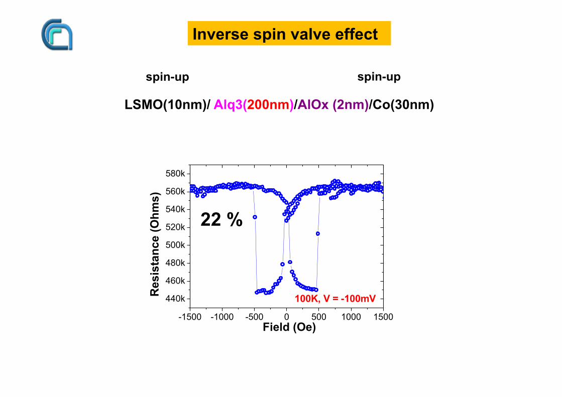
100K, V = -100mV
22 %
Inverse spin valve effect
LSMO(10nm)/ Alq3(200nm)/AlOx (2nm)/Co(30nm)
spin-up spin-up
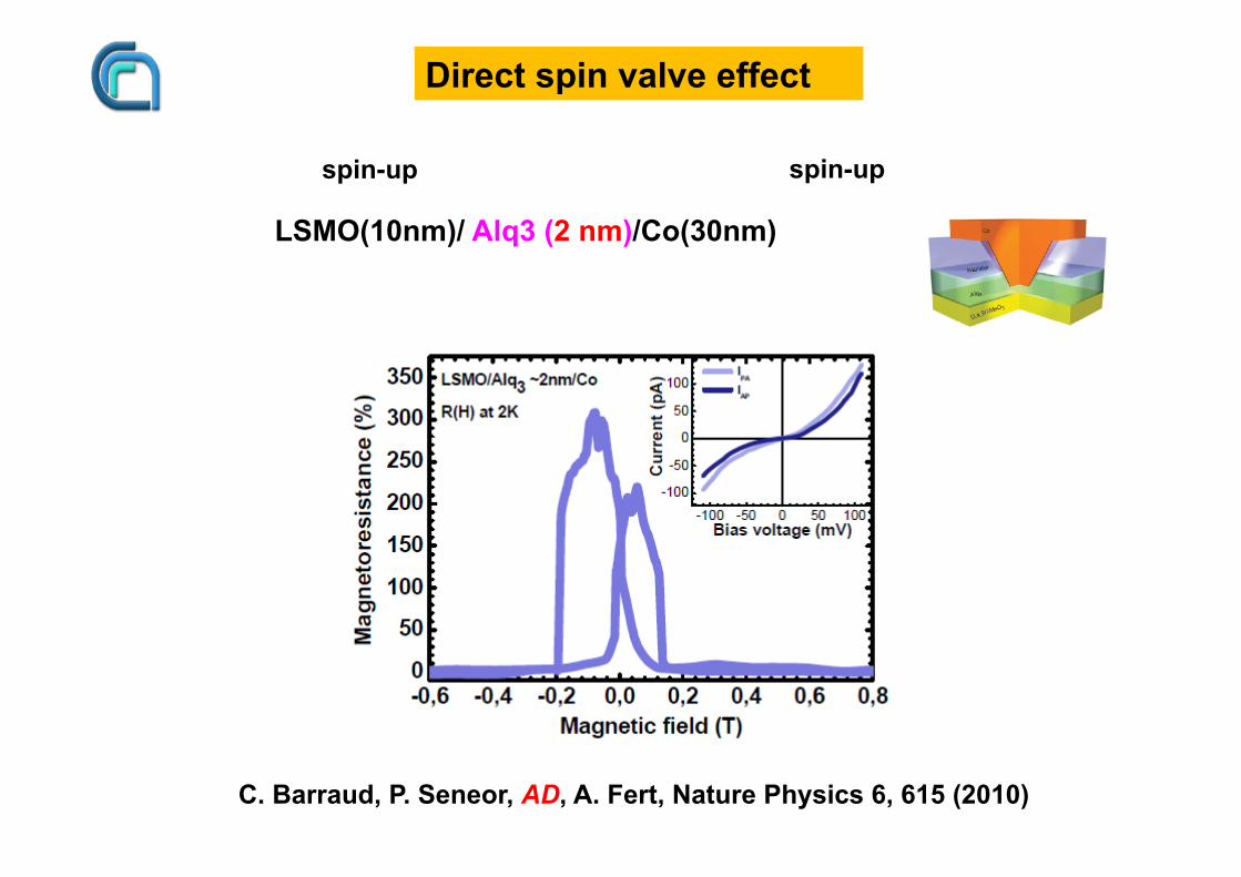
LSMO(10nm)/ Alq3 (2 nm)/Co(30nm)
spin-up spin-up
Direct spin valve effect
C. Barraud, P. Seneor, AD, A. Fert, Nature Physics 6, 615 (2010)
-1500 -1000 -500 0 500 1000 1500
440k
460k
480k
500k
520k
540k
560k
580k
Res
ista
nce
(Ohm
s)
Field (Oe)
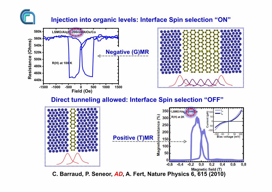
LSMO/Alq3 ∼200nm/AlOx/Co R(H) at 100 K
Injection into organic levels: Interface Spin selection “ON”
Direct tunneling allowed: Interface Spin selection “OFF”
Positive (T)MR
Negative (G)MR
C. Barraud, P. Seneor, AD, A. Fert, Nature Physics 6, 615 (2010)
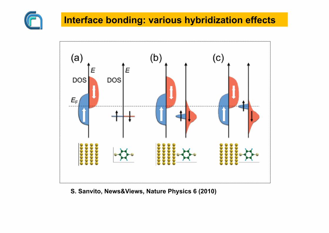
S. Sanvito, News&Views, Nature Physics 6 (2010)
Interface bonding: various hybridization effects
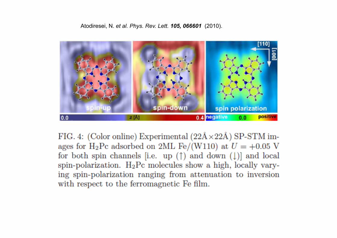
Atodiresei, N. et al. Phys. Rev. Lett. 105, 066601 (2010).
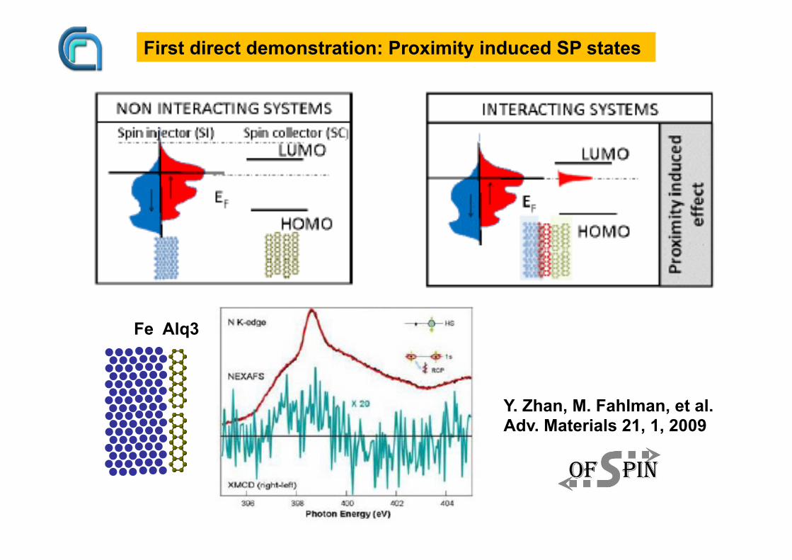
First direct demonstration: Proximity induced SP states
Y. Zhan, M. Fahlman, et al. Adv. Materials 21, 1, 2009
Fe Alq3
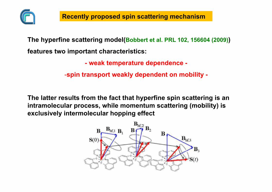
The hyperfine scattering model(Bobbert et al. PRL 102, 156604 (2009))
features two important characteristics:
- weak temperature dependence -
- spin transport weakly dependent on mobility -
The latter results from the fact that hyperfine spin scattering is an intramolecular process, while momentum scattering (mobility) is exclusively intermolecular hopping effect
Recently proposed spin scattering mechanism
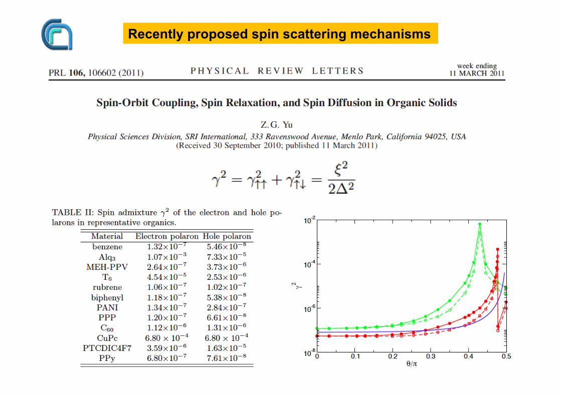
Recently proposed spin scattering mechanisms
CONCLUSIONS
Organic Spintronics it is still a young science – much to be understood Spin Injection – straightforward demonstration still missing, but many indirect evidences support that Fascinating interface physics/chemistry – many possibilities for spin-tuning at hybrid interfaces Nonetheless many questions still open – see above - new device paradigms are already coming out
Thanks to
Colleagues: I. Bergenti, A. Riminucci, M. Prezioso, P. Graziosi, F. Borgatti, A. Gambardella, R. Cecchini, E. Lunedei EC projects: OFSPIN, HINTS, IFOX MIUR: few FIRB and PRIN projects Many collaborators from differnt EU countries, USA, Japan and Russia