Embed Size (px)
Citation preview
US006451415B1
(12) United States Patent Forrest et al.
(10) Patent N0.: (45) Date of Patent:
US 6,451,415 B1 Sep. 17, 2002
(54)
(75)
(73)
(*)
(21) (22)
(63)
(51)
(52)
(58)
(56)
ORGANIC PHOTOSENSITIVE 6,198,091 B1 3/2001 Forrest et al. ......... .. 250/2141
()PTOELECTRONIC DEVICE WITH AN 6,198,092 B1 3/2001 Bulovic et al. ........ .. 250/2141 EXCITON BLOCKING LAYER 6,278,055 B1 * 8/2001 Forrest et al. ............ .. 136/263
6,297,495 B1 * 10/2001 Bulovic et al. .. 250/214.1 . ~ . 6333 458 B1 * 12/2001 Forrest et al. ............ .. 136/259
Inventors. Stephen R. Forrest, Princeton, ’ ’ . Vladimir Bulovic, Metuchen; Peter 6,352,777 B1 * 3/2002 Bulovic et al. ........ .. 428/411.1
Peumans, Princeton, all of NJ (US) OTHER PUBLICATIONS
As' :ThTrt fP'tU' 't slgnee pri?cetglns :3; €Us)nnce on mversl y’ M. Granstrom, et al., “Laminated fabrication of polymeric
’ photovoltaic diodes”, Nature, vol. 395, pp. 257—260 (Sep. Notice: Subject to any disclaimer, the term of this 17, 1998)
Patent 15 extended or adlusted under 35 G. Yu, et al., “Polymer Photovoltaic Cells: Enhanced ef? U-S~C~ 154(k)) by 0 days- ciencies via a network of internal donor—acceptor hetero
junctions”, Science, vol. 270, pp. 1789—1791 (Dec. 15, Appl. N0.: 09/449,801 1995) F?edi NOV- 26, 1999 U. Bach, et al., Solid—state dye—sensitiZed mesoporous TiO2
. . solar cells with high photon—to—electron conversion ef? Related [18' Apphcatlon Data ciencies, Nature, vol. 395, pp. 583—585 (Oct. 8, 1998).
Continuation-in-part of application No. 09/136,342, ?led on A- Shah, 6t 211-, “Photovoltaic Technology: The C2156 fOr Aug. 19, 1998, now Pat. No. 6,352,777, and a continuation- thin—?1m solar cells”, Science, vol, 285, pp, 692—698 (Jul. in-part of application No. 09/136,166, ?led on Aug. 19, 30 1999) 1998, now Pat. No. 6,297,495, and a continuation-in-part of ’ ' _ _ application No. 09/136,377, ?led on Aug. 19, 1998, now Pat. C.W. Tang, “Two—layer orgamc photovoltaic cell”, Appl. No. 6,278,055, and a continuation-in-part of application No. PhyS_ Len” 48(2), pp_ 183_185 (Jan 13, 1986) 09/136,165, ?led on Aug. 19, 1998, now Pat. No. 6,198,092, “ _ _ and a continuation-in-part of application No. 09/136,164, C~ Arbour, et 311-, Surface Chemlstnes and Photoelectro' ?led on Aug. 19, 1998, now Pat. No. 6,198,091. chemistries of Thin Film Molecular Semiconductor Mate
rials”, M01. Cryst. Liq. Cryst.,vol. 183, 307—320 (1990) (No Int. Cl.7 .............................................. .. H01L 31/06 month).
US. Cl. ..................... .. 428/212; 428/913; 136/252; (List continued on next page.) 136/263; 313/523; 257/184; 257/461
Field of Search ............................... .. 136/243, 252, gigmgtytng'loarnliifzt?gggon & Kenyon 136/263; 428/212, 913; 313/523; 257/184, ’ ’
185, 461; 252/5011 (57) ABSTRACT
References Cited Organic photosensitive optoelectronic devices (“OPODs”) U_S_ PATENT DOCUMENTS which include an exciton blocking layer to enhance device
ef?ciency. Smgle heterostructure, stacked and wave-guide 571217183 A 6/1992 ogasfiwara et a1~ ~~~~~~~~~ ~~ 357/30 type embodiments. Photodetector OPODs having multilayer
2 gohslktavra let a1‘ " structures and an exciton blocking layer. Guidelines for , , OIICS e a. - - . ,
5,350,459 A 9/1994 Suzuki et a1‘ 136/263 selection of exciton blockmg layers are provided.
5,652,067 A * 7/1997 Ito et al. ...... .. 428/690
5,703,436 A 12/1997 Forrest et al. ............ .. 313/506 24 Claims, 12 Drawing Sheets
e _/
glass ITO CuPC PTCBI BCP Ag
£2
glass ITO CuPc PTCBI Ag
US 6,451,415 B1 Page 2
OTHER PUBLICATIONS
Y. Hirose, et a1., “Chemistry and electronic properties of meta1—organic semiconductor interfaces: Al, Ti, In, Sn, Ag, and Au on PTCDA”, Phys. Rev. B, vol. 54, No. 19, pp. 13 748—13 758 (Nov. 15, 1996). D.F. O’Brien, et a1., “Improved energy transfer in electro phosphorescent devices”, Applied Physics Letters, vol. 74, No. 3, pp. 442—444, (Jan. 18, 1999). S.E. Burns, et a1., “Measurements of optical electric ?eld intensities in microcavities using thin emissive polymer ?lms”,Adv. Mater, vol. 9, No. 5, pp. 395—397 (1997) (No month). P.E. BurroWs, et a1., “Relationship BetWeen Electrolumines cence and Current Transport in organic heterojunction light—emitting devices”, J. Appl. Phys., vol. 79, No. 10, pp. 7991—8006 (May 15, 1996). S.R. Forrest, “Ultrathin Organic Films GroWn by Organic Molecular Beam Deposition and Related Techniques”, Chem. Rev., vol. 97, No. 6, 1793—1896 (Sep./Oct. 1997).
J .J . M. Halls, et a1., EXciton diffusion and dissociation in a
po1y(p—phenylenevinylene)/C6O heterojunction photovoltaic cell, Appl. Phys. Lett., 68(22), pp. 3120—3122 (May 27, 1996).
L. A. A. Pettersson, et al., “Modeling photocurrent action spectra of photovoltaic devices based on organic thin ?lms”, J. Appl. Phys., vol. 86, No. 1, pp. 487—496 (Jul. 1, 1999).
X. Deng, et a1., “Improved pc—Si p—Layer and a—Si i—Layer materials using VHF plasma deposition”, 26”1 IEEE PVSC Conf. Record, pp. 591—594, IEEE Press, NY (Sep. 30—Oct. 3, 1997).
S.R. Wenham, et a1., Applied Photovoltaics, AppendiX B, Bridge Printery, Sydney (1994) (No month).
* cited by examiner
U.S. Patent Sep. 17, 2002 Sheet 2 0f 12 US 6,451,415 B1
020: meow 023
meow meow
womm $39
\ 2am
U.S. Patent Sep. 17, 2002 Sheet 3 0f 12 US 6,451,415 B1
No 0Q “J. O O
(me) u Knsuep UOIDXS
m OE P :
8M8 wow/3 8m)\/// Sm/\,\
U.S. Patent Sep. 17, 2002 Sheet 5 0f 12 US 6,451,415 B1
800
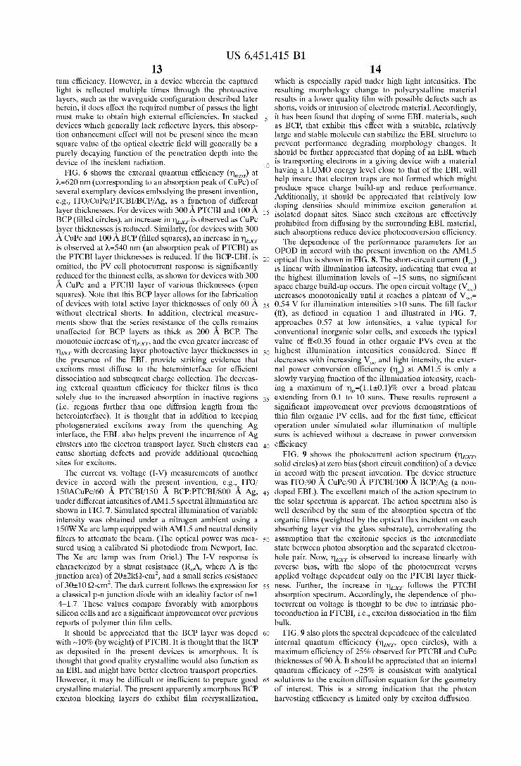
400
200 Layer Thickness (A) FIG. 6
100
(%) u ‘Kouepgg LumuenQ
U.S. Patent Sep. 17, 2002 Sheet 7 0f 12 US 6,451,415 B1
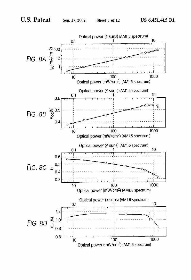
Optical power (# suns) (AM1.5 Spectrum) 1
FIG. 8A
10 100 1000 Optical power (mW/cm2) (AM1.5 spectrum)
Optical power (# suns) (AM1.5 spectrum) . 1
0-6 I I l l E I l I I l l I | ! I l l I I l l I !
10 100 1000 Optical power (mW/cmZ) (AM1.5 spectrum)
Optical power (# suns) (AM1.5 spectrum) 1
osw-yl-j ----------- - II I l I‘—I—I——I—I—I’I l — _ ‘ _ ‘I——-]--_|'—l—l—lAl—II’—_>
10 100 1000 Optical power (mW/cmZ) (AM1.5 spectrum)
Optical power (# suns) (AM1.5 spectrum) 0.1 l
I l l l I l l l I lvl I l ‘ I I l I l l l l]
l-2—-r—~§ l - - _ - - r l - < - - - * ' A - - -; - - _ l - - A 10 1/ : /'?‘\;\:
o\° .—-----; - - - - - - ~ - - - - - - - ~ - - - - - - - - - - - - - FIG. 8D ‘1 : I Foe-mg ------------------
-------------------
0.6 | | r | I | | l r | r I II r r r r l r l rI
i0 100 1000 Optical power (mW/cmz) (AM1.5 spectrum)
U.S. Patent Sep. 17, 2002 Sheet 8 0f 12 US 6,451,415 B1
(Z411 l_s 8L0l) Xnu UOIOUd
(%) u ‘Kouepgg wmueno
U.S. Patent Sep. 17, 2002 Sheet 9 0f 12 US 6,451,415 B1
52/
Q .01 $9\ \
E9\, 89
\ /89 32% \
\\ /89
82\
1| 2 52
89
U.S. Patent Sep. 17, 2002 Sheet 10 0f 12 US 6,451,415 B1
m5 .UE N
I
m I
Q. I
LO I
I ................ ........ ......... ........ ....... I52
IIIIIIII I 1 I
I
I
I
I
I
I
I
I
I
I
I
I
I
I
I
I
. I
I
I
I
I
I
I
I
I
I
I
I
I
I
I
I
I
I
I
I
I
I
I
I
I
I
I
I
I
—l I
I
I
I
I
I
I
I
Illllllll I||||n|1 C C
I'IIIIII I I
IllllIlI l
(v) wanna
IIIIIII I I l I
2&2 oi lol EQAEONWIUI I _ _ W _ _
3 .UE AEE 5922s;
com 00w ooh
US 6,451,415 B1
com
com
Sep. 17, 2002 Sheet 11 0f 12
_ _ _
U.S. Patent
uoudmsqv ‘Kouapwa LUHIUBHO
U.S. Patent Sep. 17, 2002 Sheet 12 0f 12 US 6,451,415 B1
Voltage (V) FIG. 15
I | | 1 l | | | I 1 l
'\. LO. L‘? <1’. m. N "' O o c: o o o O
Kouepgga Lumuenb |QUJ81X3
US 6,451,415 B1 1
ORGANIC PHOTOSENSITIVE OPTOELECTRONIC DEVICE WITH AN
EXCITON BLOCKING LAYER
This is a continuation-in-part application of US. patent applications With Ser. Nos. 09/136,342, 09/136,166, 09/136, 377, 09/136,165 and 09/136,164, each ?led on Aug. 19, 1998, now US. Pat. Nos. 6,352,777, 6,297,495, 6,278,055, 6,198,092 and 6,198,091, respectively.
FIELD OF INVENTION
The present invention generally relates to organic thin ?lm photosensitive optoelectronic devices. More speci?cally, it is directed to organic photosensitive optoelec tronic devices, e.g., solar cells and visible spectrum photodetectors, having an exciton blocking layer.
BACKGROUND OF THE INVENTION
Optoelectronic devices rely on the optical and electronic properties of materials to either produce or detect electro magnetic radiation electronically or to generate electricity from ambient electromagnetic radiation. Photosensitive optoelectronic devices convert electromagnetic radiation into electricity. Solar cells, also knoWn as photovoltaic (PV) devices, are speci?cally used to generate electrical poWer. PV devices are used to drive poWer consuming loads to provide, for example, lighting, heating, or to operate elec tronic equipment such as computers or remote monitoring or communications equipment. These poWer generation appli cations also often involve the charging of batteries or other energy storage devices so that equipment operation may continue When direct illumination from the sun or other ambient light sources is not available. As used herein the term “resistive load” refers to any poWer consuming or storing device, equipment or system.
Traditionally, photosensitive optoelectronic devices have been constructed of a number of inorganic semiconductors, e.g. crystalline, polycrystalline and amorphous silicon, gal lium arsenide, cadmium telluride and others. Herein the term “semiconductor” denotes materials Which can conduct elec tricity When charge carriers are induced by thermal or electromagnetic excitation. The term “photoconductive” generally relates to the process in Which electromagnetic radiant energy is absorbed and thereby converted to excita tion energy of electric charge carriers so that the carriers can conduct, i.e., transport, electric charge in a material. The terms “photoconductor” and “photoconductive material” are used herein to refer to semiconductor materials Which are chosen for their property of absorbing electromagnetic radiation of selected spectral energies to generate electric charge carriers. Solar cells are characteriZed by the effi ciency With Which they can convert incident solar poWer to useful electric poWer. Devices utiliZing crystalline or amor phous silicon dominate commercial applications and some have achieved efficiencies of 23% or greater. HoWever, ef?cient crystalline-based devices, especially of large sur face area, are dif?cult and expensive to produce due to the problems inherent in producing large crystals Without sig ni?cant ef?ciency-degrading defects. On the other hand, high ef?ciency amorphous silicon devices still suffer from problems With stability. Present commercially available amorphous silicon cells have stabiliZed ef?ciencies betWeen 4 and 8%. More recent efforts have focused on the use of organic photovoltaic cells to achieve acceptable photovol taic conversion efficiencies With economical production costs.
10
15
20
25
30
35
40
45
55
60
65
2 PV devices typically have the property that When they are
connected across a load and are irradiated by light they produce a photogenerated voltage. When irradiated Without any external electronic load, a PV device generates its maximum possible voltage, V open-circuit, or VOC. If a PV device is irradiated With its electrical contacts shorted, a maximum short-circuit current, or 156, is produced. When actually used to generate poWer, a PV device is connected to a ?nite resistive load and the poWer output is given by the current voltage product, I><V. The maximum total poWer generated by a PV device is inherently incapable of exceed ing the product, lscxVoc. When the load value is optimiZed for maximum poWer extraction, the current and voltage have values I and Vmwc respectively. A?gure of merit for solar cells is the ?ll factor ff de?ned as:
(1) I max Vim
Isc Voc
Where ff is alWays less than 1 since in actual use ISC and VOC are never obtained simultaneously. Nonetheless, as ff approaches 1, the device is more ef?cient. When electromagnetic radiation of an appropriate energy
is incident upon a semiconductive organic material, for example, an organic molecular crystal (OMC) material, or a polymer, a photon can be absorbed to produce an excited molecular state. This is represented symbolically as SO+hvQSO*. Here SO and 50* denote ground and excited molecular states, respectively. This energy absorption is associated With the promotion of an electron from a bound state in the valence band, Which may be a J'lZ-bOIld, to the conduction band, Which may be a rc*-bond, or equivalently, the promotion of a hole from the conduction band to the valence band. In organic thin-?lm photoconductors, the generated molecular state is generally believed to be an exciton, i.e., an electron-hole pair in a bound state Which is transported as a quasi-particle. The excitons can have an appreciable life-time before geminate recombination, Which refers to the process of the original electron and hole recombining With each other as opposed to recombination With holes or electrons from other pairs. To produce a photocurrent the electron-hole pair must become separated. If the charges do not separate, they can recombine in a geminant recombination process, also knoWn as quenching, either radiatively—re-emitting light of a loWer than incident light energy-, or non-radiatively—With the production of heat.
Either of these outcomes is undesirable in a photosensi tive optoelectronic device. While exciton ioniZation, or dissociation, is not completely understood, it is generally believed to occur at defects, impurities, contacts, interfaces or other inhomogeneities. Frequently, the ioniZation occurs in the electric ?eld induced around a crystal defect, denoted, M. This reaction is denoted SO*+MQe+h+. If the ioniZation occurs at a random defect in a region of material Without an overall electric ?eld, the generated electron-hole pair Will likely recombine. To achieve a useful photocurrent, the electron and hole must be collected separately at respective opposing electrodes, Which are frequently referred to as contacts. Exciton dissociation occurs either in high electric ?eld regions by ?eld-emission, or at an interface betWeen, e.g., donor-like and acceptor-like materials such as copper phthalocyanine (CuPc) and 3,4,9,10 perylenetetracarboxylic-bis-benZimidaZole (PTCBI), by charge transfer. The latter can be vieWed as an exothermic chemical reaction, i.e., a reaction in Which some energy is released as vibrational energy. This reaction occurs because
US 6,451,415 B1 3
the energy separation of the dissociated exciton, i.e., the energy difference betWeen the free electron in, e.g., PTCBI, and the free hole in, e.g., CuPc, is smaller than the energy of the exciton prior to dissociation.
Electric ?elds or inhomogeneities at a contact may cause an exciton to quench rather than dissociate, resulting in no net contribution to the current. Therefore, it is desirable to keep photogenerated excitons aWay from the contacts. This has the effect of limiting the diffusion of excitons to the region near the junction so that the junction associated electric ?eld has an increased opportunity to separate charge carriers liberated by the dissociation of the excitons near the junction.
Here appreciation should be taken of some of the distinc tions betWeen organic photosensitive optoelectronic devices (OPODs) and organic light emitting devices (OLEDs). In an OLED, a bias is applied to a device to produce a How of holes and electrons into a device. In OLEDs, excitons are generally formed Which in time may either recombine radiatively or nonradiatively. In OLEDs, maximum radiative recombination is the desired result. In OPODs maximum exciton generation and dissociation is the desired result. The differing objectives of the devices lead to differing selection of materials and layer thicknesses. OPOD photosensitive materials are chosen for their absorption properties While photoluminescent materials for OLEDs are chosen for their emissive properties.
To produce internally generated electric ?elds Which occupy a substantial volume, the usual method is to juxta pose tWo layers of material With appropriately selected conductive properties, especially With respect to their dis tribution of molecular quantum energy states. The interface of these tWo materials is called a photovoltaic heterojunc tion. In traditional semiconductor theory, materials for form ing PV heterojunctions have been denoted as generally being of either n, or donor, type or p, or acceptor, type. Here n-type denotes that the majority carrier type is the electron. This could be vieWed as the material having many electrons in relatively free energy states. The p-type denotes that the majority carrier type is the hole. Such material has many holes in relatively free energy states. The type of the background, i.e., not photogenerated, majority carrier con centration depends primarily on unintentional doping by defects or impurities. The type and concentration of impu rities determine the value of the Fermi energy, or level, Within the gap betWeen the highest occupied molecular orbital (HOMO) and the loWest unoccupied molecular orbital (LUMO), called the HOMO-LUMO gap. The Fermi energy characteriZes the statistical occupation of molecular quantum energy states denoted by the value of energy for Which the probability of occupation is equal to 1/2. A Fermi energy near the LUMO energy indicates that electrons are the predominant carrier. A Fermi energy near the HOMO energy indicates that holes are the predominant carrier. Accordingly, the Fermi energy is a primary characteriZing property of traditional semiconductors and the prototypical PV heterojunction has traditionally been the p-n interface.
In addition to relative free-carrier concentrations, a sig ni?cant property in organic semiconductors is carrier mobil ity. Mobility measures the ease With Which a charge carrier can move through a conducting material in response to an electric ?eld. As opposed to free carrier concentrations, carrier mobility is determined in large part by intrinsic properties of the organic material such as crystal symmetry and periodicity. Appropriate symmetry and periodicity can produce higher quantum Wavefunction overlap of HOMO levels producing higher hole mobility, or similarly, higher
10
15
25
35
45
55
65
4 overlap of LUMO levels to produce higher electron mobil ity. Moreover, the donor or acceptor nature of an organic semiconductor, e.g., 3,4,9,10-perylenetetracarboxylic dian hydride (PTCDA), may be at odds With the higher carrier mobility. For example, While chemistry arguments suggest a donor, or n-type, character for PTCDA, experiments indicate that hole mobilities exceed electron mobilities by several orders of magnitude so that the hole mobility is a critical factor. The result is that device con?guration predictions from donor/acceptor criteria may not be borne out by actual device performance. Due to these unique electronic proper ties of organic materials, rather than designating them as “p-type” or “acceptor-type” and “n-type” or “donor-type”, the nomenclature of “hole-transporting-layer” (HTL) or “electron-transporting-layer” (ETL) is frequently used. In this designation scheme, an ETL Will preferentially be electron conducting and an HTL Will preferentially be hole transporting. The term “rectifying” denotes, inter alia, that an interface has an asymmetric conduction characteristic, i.e., the interface supports electronic charge transport pref erably in one direction. Recti?cation is associated normally With a built-in electric ?eld Which occurs at the heterojunc tion betWeen appropriately selected materials. The electrodes, or contacts, used in a photosensitive
optoelectronic device are an important consideration. In a photosensitive optoelectronic device, it is desirable to alloW the maximum amount of ambient electromagnetic radiation from the device exterior to be admitted to the photoconduc tively active interior region. That is, it is desirable to get the electromagnetic radiation to Where it can be converted to electricity by photoconductive absorption. This often dic tates that at least one of the electrical contacts should be minimally absorbing and minimally re?ecting of the inci dent electromagnetic radiation. That is, such contact should be substantially transparent. When used herein, the terms “electrode” and “contact” refer only to layers that provide a medium for delivering photogenerated poWer to an external circuit or providing a bias voltage to the device. That is, an electrode, or contact, provides the interface betWeen the photoconductively active regions of an organic photosensi tive optoelectronic device and a Wire, lead, trace or other means for transporting the charge carriers to or from the external circuit. The term “charge transfer layer” is used herein to refer to layers similar to but different from elec trodes in that a charge transfer layer only delivers charge carriers from one subsection of an optoelectronic device to the adjacent subsection. As used herein, a layer of material or a sequence of several layers of different materials is said to be “transparent” When the layer or layers permit at least 50% of the ambient electromagnetic radiation in relevant Wavelengths to be transmitted through the layer or layers. Similarly, layers Which permit some but less that 50% transmission of ambient electromagnetic radiation in rel evant Wavelengths are said to be “semi-transparent”.
Electrodes or contacts are usually metals or “metal sub stitutes”. Herein the term “metal” is used to embrace both materials composed of an elementally pure metal, e.g., Mg, and also metal alloys Which are materials composed of tWo or more elementally pure metals, e.g., Mg and Ag together, denoted Mg:Ag. Here, the term “metal substitute” refers to a material that is not a metal Within the normal de?nition, but Which has the metal-like properties that are desired in certain appropriate applications. Commonly used metal substitutes for electrodes and charge transfer layers Would include doped Wide bandgap semiconductors, for example, trans parent conducting oxides such as indium tin oxide (ITO), gallium indium tin oxide (GITO), and Zinc indium tin oxide
US 6,451,415 B1 5
(ZITO). In particular, ITO is a highly doped degenerate n+ semiconductor With an optical bandgap of approximately 3.2 eV rendering it trans arent to Wavelengths greater than approximately 3900 A. Another suitable metal substitute material is the transparent conductive polymer polyanaline (PANI) and its chemical relatives. Metal substitutes may be further selected from a Wide range of non-metallic materials, Wherein the term “non-metallic” is meant to embrace a Wide range of materials provided that the material is free of metal in its chemically uncombined form. When a metal is present in its chemically uncombined form, either alone or in combination With one or more other metals as an alloy, the
metal may alternatively be referred to as being present in its metallic form or as being a “free metal”. Thus, the metal substitute electrodes of the present invention may sometimes be referred to as “metal-free” Wherein the term “metal-free” is expressly meant to embrace a material free of metal in its chemically uncombined form. Free metals typically have a form of metallic bonding that may be thought of as a type of chemical bonding that results from a sea of valence electrons Which are free to move in an electronic conduction band throughout the metal lattice. While metal substitutes may contain metal constituents they are “non-metallic” on sev eral bases. They are not pure free-metals nor are they alloys of free-metals. When metals are present in their metallic form, the electronic conduction band tends to provide, among other metallic properties, a high electrical conduc tivity as Well as a high re?ectivity for optical radiation.
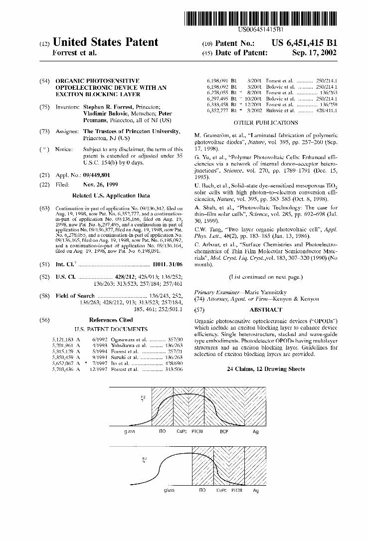
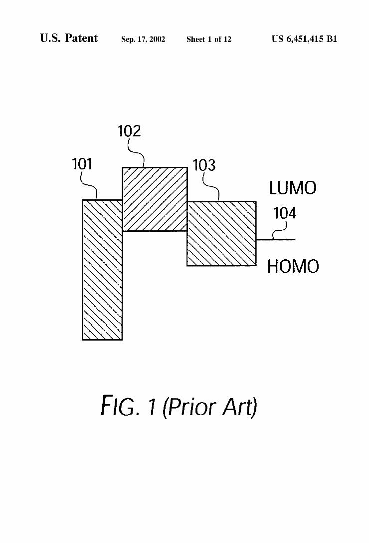
Atypical prior art photovoltaic device con?guration is the organic bilayer cell. In the bilayer cell, charge separation predominantly occurs at the organic heterojunction. The built-in potential is determined by the HOMO-LUMO gap energy difference betWeen the tWo materials contacting to form the heterojunction. The HOMO-LUMO energy levels for such a heterojunction are illustrated schematically in FIG. 1 Where 101 represents an anode, 102 represents an HTL layer, 103 represents an ETL layer and 104 represents a cathode. The HOMO-LUMO gap offset betWeen the HTL and ETL produce an electric ?eld around the HTL/ETL interface.
Herein, the term “cathode” is used in the folloWing manner. In a non-stacked PV device or a single unit of a stacked PV device under ambient irradiation and connected With a resistive load and With no externally applied voltage, e.g., a solar cell, electrons move to the cathode from the adjacent photoconducting material. Similarly, the term “anode” is used herein such that in a solar cell under illumination, holes move to the anode from the adjacent photoconducting material, Which is equivalent to electrons moving in the opposite manner. It Will be noted that as the terms are used herein anodes and cathodes may be elec trodes or charge transfer layers.
Organic PV devices typically have relatively loW quan tum yield (the ratio of photons absorbed to carrier pairs generated, or electromagnetic radiation to electricity con version ef?ciency), being on the order of 1% or less. This is, in part, thought to be due to the second order nature of the intrinsic photoconductive process, that is, carrier generation requires exciton generation, diffusion and ioniZation, as described above. In order to increase these yields, materials and device con?gurations are desirable Which can enhance the quantum yield and, therefore, the poWer conversion ef?ciency. Thompson et al. in US. patent application Ser. No.
09/311,126, noW abandoned, for “Very High Ef?ciency Organic Light Emitting Devices Based on Electrophospho rescence” have described the use of an exciton blocking
10
15
20
25
30
35
40
45
50
55
60
65
6 layer to con?ne excitons to the emission layer in an organic light emitting device (OLED) in order to increase the device ef?ciency. In the context of the present invention, an EBL is characteriZed by its ability to prevent the diffusion of exci tons from an adjacent organic layer into or across the EBL. “Ultrathin Organic Films Grown by Organic Molecular Beam Deposition and Related Techniques”, Chemical Reviews, Vol. 97, No. 6, 1997 (hereinafter Forrest, Chem. Rev. 1997) and Arbour, C., Armstrong, N. R., Brina, R., Collins, G., DanZiger, J. -P., Lee, R, Nebesny, K. W., PankoW, J ., Waite, S., “Surface Chemistries and Photoelec trochemistries of Thin Film Molecular Semiconductor Materials”, Molecular Crystals and Liquid Crystals, 1990, 183, 307, (hereinafter Arbour et al.), disclose that alternating thin multilayer stacks of similar type photoconductors could be used to enhance photogenerated carrier collection ef? ciency over that using a single layer structure. Further, these sources describe multiple quantum Well (MQW) structures in Which quantum siZe effects occur When the layer thick nesses become comparable to the exciton dimensions.
SUMMARY AND OBJECTS OF INVENTION
Several guidelines must be kept in mind in designing an ef?cient organic photosensitive optoelectronic device. It is desirable for the exciton diffusion length, LD, to be greater than or comparable to the layer thickness, L, since it is believed that most exciton dissociation Will occur at an interface. If LD is less than L, then many excitons may recombine before dissociation. It is further desirable for the total photoconductive material thickness to be of the order of the electromagnetic radiation absorption length, 1/ot (Where 0t is the absorption coef?cient), so that nearly all of the radiation incident on the solar cell is absorbed to produce excitons. HoWever, the thickness should not be so large compared to the extent of the heterojunction electric ?elds that many excitons get generated in a ?eld-free region. One reason for this is that the ?elds help to dissociate the excitons. Another reason is that if an exciton dissociates in a ?eld-free region, it is more likely to suffer geminant recombination, or quenching, and contribute nothing to the photocurrent. Further, electric ?elds may exist at the electrode/semiconductor interfaces. These ?elds at the elec trode interfaces can also promote exciton quenching. Furthermore, the photoconductive layer thickness should be as thin as possible to avoid excess series resistance due to the high bulk resistivity of organic semiconductors. On the other hand, another countervailing consideration is
that as the separation betWeen the exciton dissociating interface and the adjacent electrodes increases, the electric ?eld region around the interface Will have a higher value over a greater volume. Since light absorption increases With increasing electric ?eld strength, more excitons Will be generated. Also, the higher electric ?elds Will also promote faster exciton dissociation.
It has been suggested that one means for circumventing the diffusion length limitation is to use thin cells With multiple or highly folded interfaces, such as can be achieved using nanotextured materials, polymer blends, closely spaced, repeated interfaces, or spatially distributed dissocia tion sites. To date, none of these proposals has led to a signi?cant improvement in overall performance of solar cells, particularly at high illumination intensities.
Accordingly, in the present invention higher internal and external quantum ef?ciencies have been achieved by the inclusion in OPODs of one or more exciton blocking layers (EBLs) to con?ne photogenerated excitons to the region
US 6,451,415 B1 7
near the dissociating interface and prevent parasitic exciton quenching at a photosensitive organic/electrode interface. In addition to limiting the volume over Which excitons may diffuse, an EBL can also act as a diffusion barrier to substances introduced during deposition of the electrodes. In some circumstances, an EBL can be made thick enough to ?ll pinholes or shorting defects Which could otherWise render an OPOD non-functional. An exciton blocking layer can therefore help protect fragile organic layers from dam age produced When electrodes are deposited onto the organic materials.
It is believed that the EBLs comprising the present invention derive their exciton blocking property from having a LUMO-HOMO energy gap substantially larger than that of the adjacent organic semiconductor from Which excitons are being blocked. The thus con?ned excitons are prohibited from existing in the EBL due to quantum energy consider ations. While it is desirable for the EBL to block excitons, it is not desirable for the EBL to block all charge carrying quanta as Well. HoWever, due to the nature of the adjacent energy levels an EBL Will necessarily block one sign of charge carrier. By design, an EBL Will alWays exist betWeen tWo adjacent layers, usually an organic photosensitive semi conductor layer and a electrode or charge transfer layer. The adjacent electrode or charge transfer layer Will be in context either a cathode or an anode. Therefore, the material for an EBL in a given position in a device Will be chosen so that the desired sign of carrier Will not be impeded in its transport to the electrode or charge transfer layer. Proper energy level alignment ensures that no barrier to charge transport exists, preventing an increase in series resistance. It should be appreciated that the exciton blocking nature of a material is not an intrinsic property. Whether a given material Will act as an exciton blocker depends upon the relative HOMO and LUMO levels of the adjacent organic photosensitive mate rial. Therefore, it is not possible to identify a class of compounds in isolation as exciton blockers Without regard to the device context in Which they may be used. HoWever, With the teachings herein one of ordinary skill in the art may identify Whether a given material Will function as an exciton blocking layer When used With a selected set of materials to construct an OPOD.
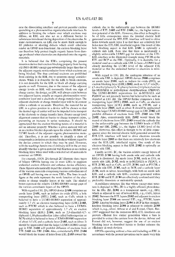
For example, FIGS. 2A through 2C illustrate three types of bilayer OPODs having one or more EBLs to suppress undesired exciton diffusion and enhance device ef?ciency. These ?gures schematically depict the relative energy levels of the various materials comprising various embodiments of an OPOD cell having one or more EBLs. The lines in each ?gure at the ends represent the Work function of the elec trodes or charge transfer layers at the ends. The shaded boxes represent the relative LUMO-HOMO energy gaps of the various constituent layers of the OPOD.
With regard to FIG. 2A, OPOD device 2A00 comprises an anode layer 2A01, such as indium tin oxide (ITO), a hole transporting layer (HTL) 2A02, such as CuPc Which is believed to have a LUMO-HOMO separation of approxi mately 1.7 eV, an electron transporting layer 2A03, such as PTCBI Which is also believed to have a LUMO HOMO separation of approximately 1.7 eV, an exciton blocking layer (EBL) 2A04, such as 2,9-dimethyl-4,7 diphenyl-1,10-phenanthroline (also called bathocuproine or BCP) Which is believed to have a LUMO-HOMO separation of about 3.5 eV, and a cathode layer 2A05, such as silver. It should be appreciated that the larger LUMO-HOMO energy gap in EBL 2A04 Will prohibit diffusion of excitons from ETL 2A03 into EBL 2A04. Also, coincidentally EBL 2A04 Would block the transit of holes from ETL 2A03 toWard the
10
15
25
35
45
55
65
8 cathode due to the unfavorable gap betWeen the HOMO levels of ETL 2A03 and EBL 2A04, i.e., the higher ioniZa tion potential of the EBL. HoWever, this effect is thought to be of little consequence since the internal electric ?eld generated around the HTL/ETL interface Will tend to drive holes toWards anode layer 1 so that there are relatively feW holes near the ETL/EBL interfacial region. One result of this hole blocking aspect is that EBL 2A04 is optimally a cathode side EBL. Note also that there is incidentally a slightly unfavorable LUMO gap for electrons at the ETL/ EBL interface in the illustrated example using PTCBI as the ETL and BCP as the EBL. Optimally, it is desirable for a material used as a cathode side EBL to have a LUMO level closely matching the LUMO level of the adjacent ETL material so that the undesired barrier to electrons is mini miZed. With regard to FIG. 2B, the analogous situation of an
anode side EBL is depicted. OPOD device 2B00 comprises an anode layer 2B01, such as indium tin oxide (ITO), an exciton blocking layer (EBL) 2B02, such as 4,4‘,4“-tris{N, (3-methylphenyl)-N-phenylamino}triphenylamine (m-MTDATA) or polyethylene dioxythiophene (PEDOT). The LUMO-HOMO separations for m-MTDATA and PEDOT are not precisely knoWn but believed to be such as depicted in FIG. 2B. The OPOD further comprises a hole transporting layer (HTL) 2B03, such as CuPc, an electron transporting layer (ETL) 2B04, such as PTCBI, and a cathode layer 2B05, such as silver. It should be appreciated that the larger LUMO-HOMO energy gap in EBL 2B02 Will prohibit diffusion of excitons from HTL 2B03 into EBL 2B02. Also, coincidentally EBL 2B02 Would block the transit of electrons from HTL 2B03 toWard the cathode due to the unfavorable gap betWeen the LUMO levels of HTL 2B03 and EBL 2B02, i.e., the higher LUMO level of the EBL. HoWever, this effect is thought to be of little conse quence since the internal electric ?eld generated around the HTL/ETL interface Will tend to drive electrons toWards cathode layer 2B05 so that there are relatively feW electrons near the HTL/EBL interfacial region. One result of this electron blocking aspect is that EBL 2B02 is optimally an anode side EBL.
Finally, in FIG. 2C, the various relative energy layers of an OPOD 2C00 having both anode side and cathode side EBLs is illustrated. An anode layer 2C01, such as ITO, an anode side EBL 2C02, such as m-MTDATA or PEDOT, a HTL 2C03, such as CuPc, an ETL 2C04, such as PTCBI, a cathode side EBL 2C05, such as BCP, and a cathode layer 2C06, such as silver. Accordingly, With both an anode side EBL and a cathode side EBL, excitons generated Within HTL 2C03 and ETL 2C04 are effectively con?ned until they preferably dissociate or undesirably quench. A multilayer structure like that Whose energy state struc
ture is depicted in FIG. 2D is a highly ef?cient photodetec tor. In FIG. 2D, 2D01 is a transparent anode, e.g., ITO, Which is adjacent to one of several HTL, e.g., CuPc, layers 2D02. BetWeen the HTL layers 2D02 and adjacent to exciton blocking layer 2D04 are several ETL, e.g., PTCBI, layers 2D03. Exciton blocking layer 2D04 is BCP in this example. Exciton blocking layer 2D04 is adjacent to cathode 2D05 Which is, e.g., silver. Arbour et al and Forrest, Chem. Rev. 1997 suggested that the numerous HTL-ETL interfaces can provide ef?cient free carrier generation When a bias is provided to extract the carriers from the device. Arbour and Forrest did not, hoWever, suggest the use of an exciton blocking layer as described herein to further enhance the ef?ciency in such devices. OPODs operating Without a bias and including an EBL in
accordance With the present invention can be made very thin
US 6,451,415 B1 9
Without severe loss of photocurrent. Accordingly, OPODs including EBLs may be used in combination With the highly ef?cient OPODs of the US. patent applications of Forrest et al., noW Pat. Nos. 6,352,777, 6,297,495, 6,278,055, 6,198, 092 and 6,198,091, (hereinafter collectively “Forrest OPOD Appls.”) Which are incorporated herein by reference in their entirety. Stacked OPODs including EBLs and having numer ous subcells and/or including a Waveguide con?guration may be constructed in accord With the present invention to achieve high internal and external quantum ef?ciencies. When the term “subcell” is used hereafter, it refers to an
organic photosensitive optoelectronic construction Which may include an exciton blocking layer in accordance With the present invention. When a subcell is used individually as a photosensitive optoelectronic device, it typically includes a complete set of electrodes, i.e., positive and negative. As disclosed herein, in some stacked con?gurations it is pos sible for adjacent subcells to utiliZe common, i.e., shared, electrode or charge transfer layers. In other cases, adjacent subcells do not share common electrodes or charge transfer layers. The term “subcell” is disclosed herein to encompass the subunit construction regardless of Whether each subunit has its oWn distinct electrodes or shares electrodes or charge transfer layers With adjacent subunits. Herein the terms “cell”, “subcell”, “unit”, “subunit”, “section”, and “subsec tion” are used interchangeably to refer to a photoconductive layer or set of layers and the adjoining electrodes or charge transfer layers. As used herein, the terms “stack”, “stacked”, “multisection” and “multicell” refer to any optoelectronic device With multiple layers of a photoconductive material separated by one or more electrode or charge transfer layers.
Since the stacked subcells of the solar cell may be fabricated using vacuum deposition techniques that alloW external electrical connections to be made to the electrodes separating the subcells, each of the subcells in the device may be electrically connected either in parallel or in series, depending on Whether the poWer and/or voltage generated by the solar cell is to be maximiZed. The improved external quantum ef?ciency that may be achieved for stacked solar cell embodiments of the present invention may also be attributed to the fact that the subcells of the stacked solar cell may be electrically connected in parallel since a parallel electrical con?guration permits substantially higher ?ll fac tors to be realiZed than When the subcells are connected in series.
Although the high series resistance of photoconductive organic materials inhibits use of subcells in a series con ?guration for high poWer applications, there are certain applications, for example, in operating liquid crystal dis plays (LCD), for Which a higher voltage may be required, but only at loW current and, thus, at loW poWer levels. For this type of application, stacked, series-connected solar cells may be suitable for providing the required voltage to the LCD. In the case When the solar cell is comprised of subcells electrically connected in series so as to produce such a higher voltage device, the stacked solar cell may be fabri cated so as to have each subcell producing approximately the same current so to reduce inef?ciency. For example, if the incident radiation passes through in only one direction, the stacked subcells may have an increasing thickness With the outermost subcell, Which is most directly exposed to the incident radiation, being the thinnest. Alternatively, if the subcells are superposed on a re?ective surface, the thick nesses of the individual subcells may be adjusted to account for the total combined radiation admitted to each subcell from the original and re?ected directions.
Further, it may be desirable to have a direct current poWer supply capable of producing a number of different voltages.
10
15
20
25
30
35
40
45
50
55
60
65
10 For this application, external connections to intervening electrodes could have great utility. Accordingly, in addition to being capable of providing the maximum voltage that is generated across the entire set of subcells, an exemplary embodiment the stacked solar cells of the present invention may also be used to provide multiple voltages from a single poWer source by tapping a selected voltage from a selected subset of subcells.
Representative embodiments may also comprise transpar ent charge transfer layers. As described herein charge trans fer layers are distinguished from ETL and HTL layers by the fact that charge transfer layers are frequently, but not necessarily, inorganic and they are generally chosen not to be photoconductively active.
Embodiments of the present invention may include, as one or more of the transparent electrodes of the optoelec tronic device, a highly transparent, non-metallic, loW resis tance cathode such as disclosed in Us. patent application Ser. No. 09/054,707 to Parthasarathy et al. (“Parasarathy ’707”) , or a highly ef?cient, loW resistance metallic/non metallic composite cathode such as disclosed in US. Pat. No. 5,703,436 to Forrest et al. (“Forrest ’436”). Each type of cathode is preferably prepared in a fabrication process that includes the step of sputter depositing an ITO layer onto either an organic material, such as copper phthalocyanine (CuPc), PTCDA and PTCBI, to form a highly transparent, non-metallic, loW resistance cathode or onto a thin MgzAg layer to form a highly ef?cient, loW resistance metallic/non metallic composite cathode. Parasarathy ’707 discloses that an ITO layer onto Which an organic layer had been deposited, instead of an organic layer onto Which the ITO layer had been deposited, does not function as an ef?cient cathode.
It is an object of the present invention to provide an OPOD and an OPOD subcell comprising one or more exciton blocking layers to increase the internal quantum ef?ciency of the OPOD or OPOD subcell.
It is an object of the present invention to provide an OPOD capable of operating With a high external quantum ef?ciency and comprising stacked OPOD subcells.
It is another object of the present invention to provide a stacked OPOD capable of operating With an external quan tum efficiency that approaches the maximum internal quan tum ef?ciency of an optimal OPOD subcell.
Another object of the present invention is to provide an OPOD With improved absorption of incident radiation for more ef?cient photogeneration of charge carriers.
It is a further objective of the present invention to provide an OPOD With an improved VOC and an improved ISC. Another object of the present invention is to provide a
stacked OPOD having parallel electrical interconnection of the subcells. A further object of the present invention is to provide a
stacked OPOD comprised of multiple organic OPOD sub cells With transparent electrodes and having a substantially re?ective bottom layer to increase overall electromagnetic radiation absorption by capturing the electromagnetic radia tion re?ected by the bottom layer. A further object of the present invention is to provide a
Waveguide con?guration OPOD having an exciton blocking layer.
Yet another object of the present invention is to provide OPODs including a conductive or an insulating substrate.
A further object of the present invention is to provide OPODs including a rigid or a ?exible substrate.
US 6,451,415 B1 11
A further object of the present invention is to provide OPODs Wherein the organic materials used are polymeric or non-polymeric thin ?lms.
BRIEF DESCRIPTION OF THE DRAWINGS
The foregoing and other features of the present invention Will be more readily apparent from the following detailed description of exemplary embodiments taken in conjunction With the attached draWings.
FIG. 1 illustrates the relative energy levels in a typical prior art device.
FIGS. 2A—2C illustrate the relative energy levels in exemplary embodiments of the invention having a cathode side EBL, an anode side EBL, or both.
FIG. 2D illustrates the relative energy levels in an exem plary embodiment of a multilayer photodetector having an EBL on the cathode side.
FIG. 3 depicts an exemplary OPOD in accord With the present invention.
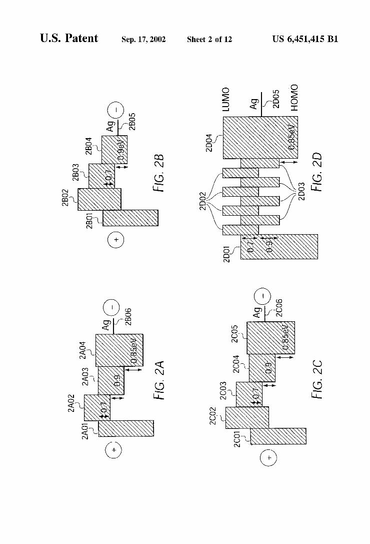
FIG. 4 is a graph of calculated exciton density pro?les comparing the effect of an EBL With the effect of an exciton quenching interface.
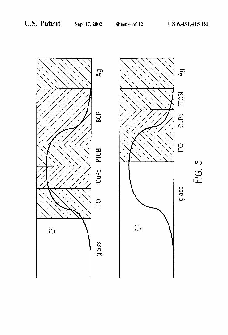
FIG. 5 depicts an effect of the eBL to shift the active region of exciton dissociation to the region of maximum optical electric ?eld intensity.
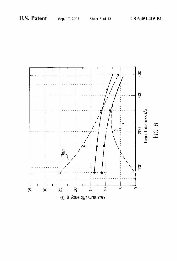
FIG. 6 is a graph of measured external quantum ef?ciency next) at )\.=620 nm of ITO/CuPc/PTCBI/BCP/Ag devices as a function of different layer thicknesses.
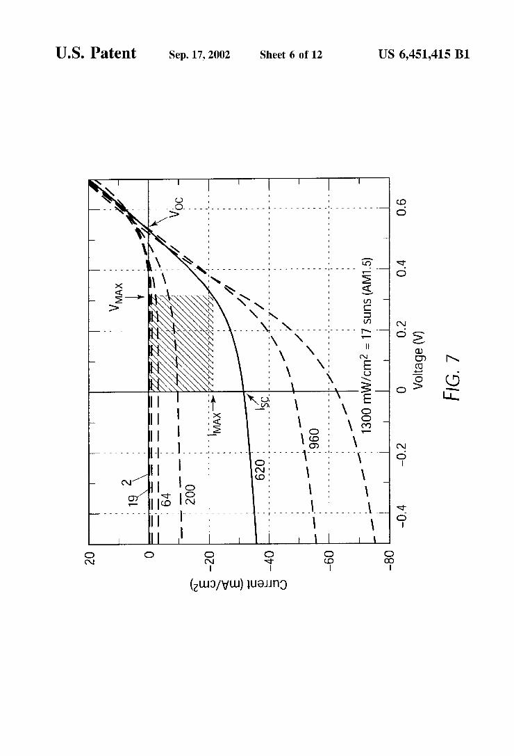
FIG. 7 is a graph of current vs. voltage (I-V) measure ments of aothin device incorporating an EBL o(ITO/150 A CuPc/160 A PTCBI/150 A BCP1PTCBI/800 A Ag) under different intensities of AM1.5 spectral illumination.
FIG. 8 illustrates an exemplary embodiment of a stacked OPOD in accord With the present invention.
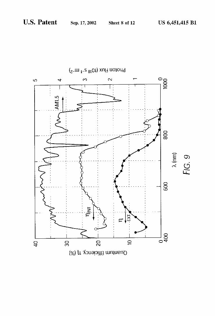
FIG. 9 illustrates an exemplary embodiment of a Wave guide geometry type OPOD in accord With the present invention.
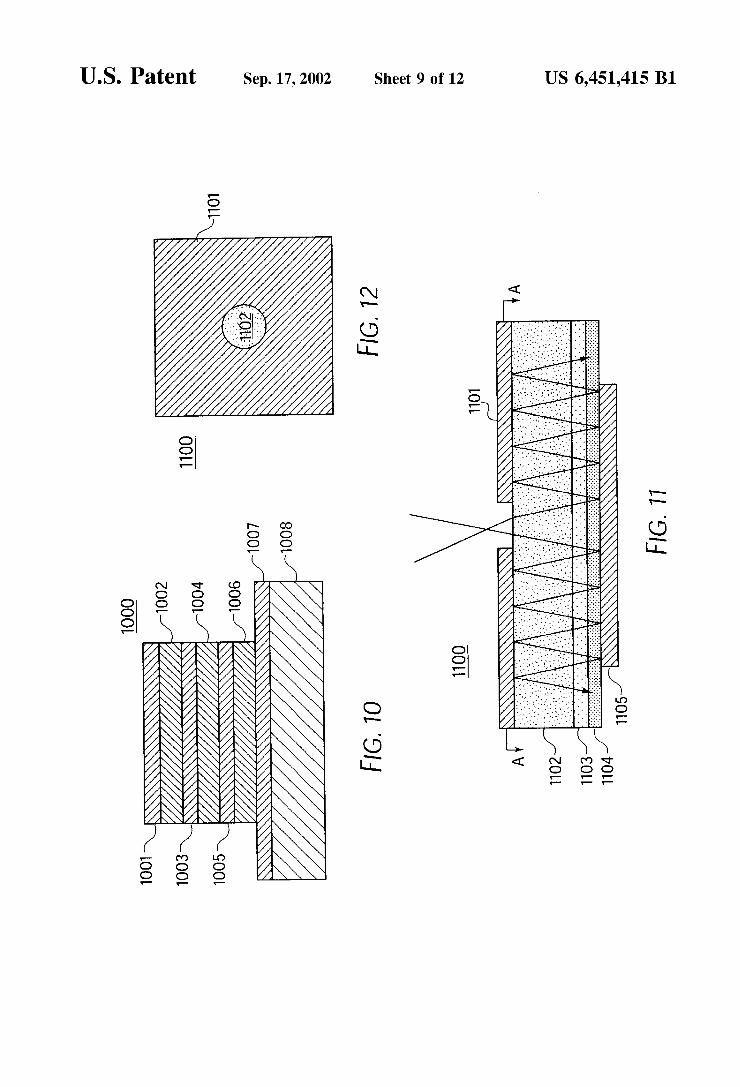
FIG. 10 schematically depicts a stacked OPOD having an exciton blocking layer.
FIG. 11 depicts a Waveguide type OPOD having an exciton blocking layer.
FIG. 12 is a top doWn vieW of FIG. 12 through line A—A.
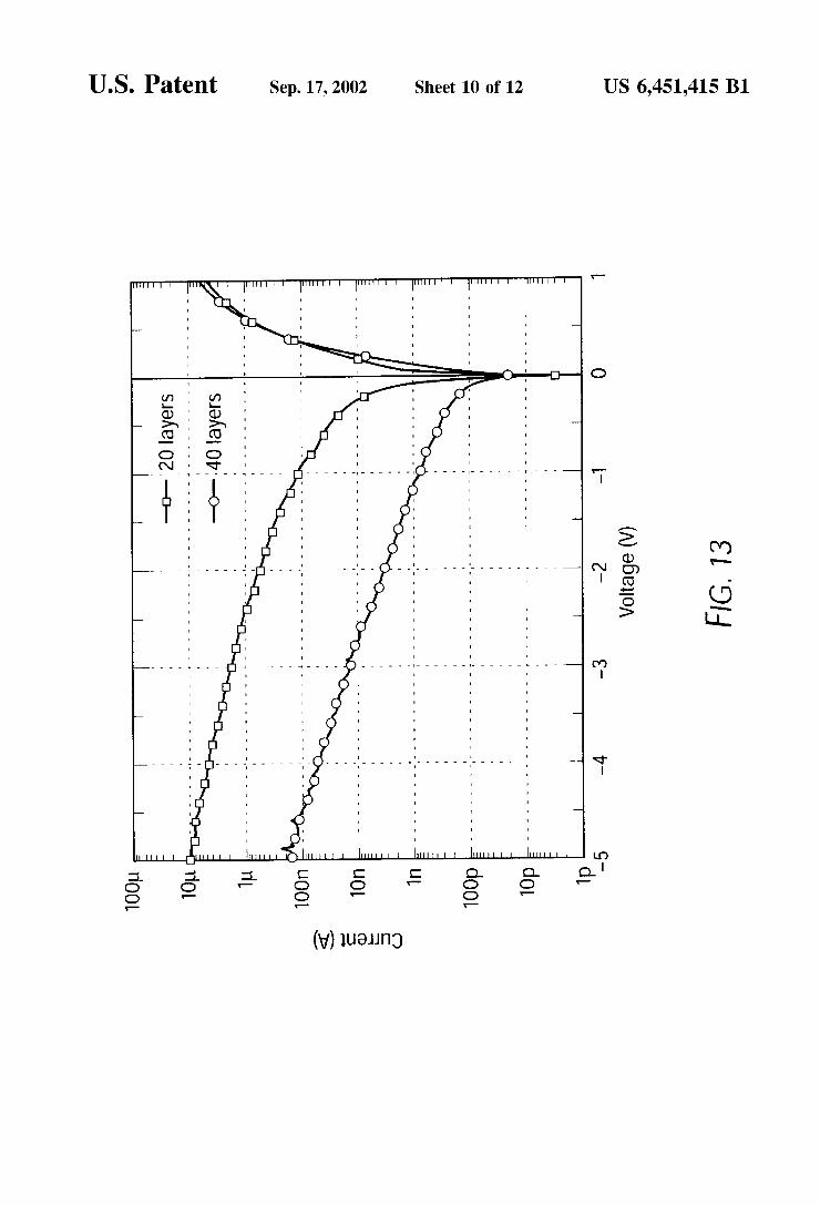
FIG. 13 is a graph of current/voltage characteristics of some multilayer photodetectors in accord With the present invention.
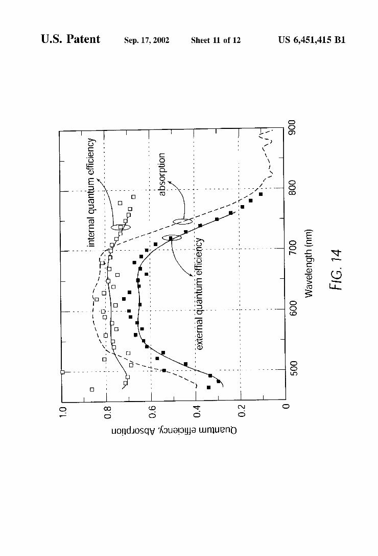
FIG. 14 is a plot of some ef?ciency and absorption data as a function of incident Wavelength for a multilayer photode tector in accord With the present invention.
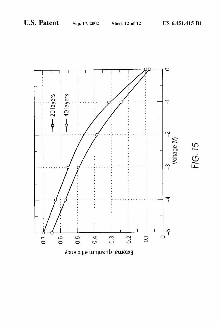
FIG. 15 is plot of external quantum ef?ciency as a function of voltage for some multilayer photodetectors in accord With the present invention.
DETAILED DESCRIPTION
Devices have been constructed and example data recorded for exemplary embodiments of the present invention, in particular, the device depicted in FIG. 3.
In FIG. 3, OPOD 300 has cathode 301 of a suitable electrode material such as silver, an EBL 302 of a suitable material such as BCP, an ETL 303 such as PTCBI, a HTL 304 such as CuPc, and an anode of a suitable electrode material such as ITO. In such a device at least one of the electrodes must be transparent to alloW the admission of electromagnetic radiation. Hereafter, calculations and data
10
15
25
35
45
55
65
12 are presented from actual devices and compared to prior art and theory. Other prospective embodiments of devices in accord With the present invention are also described. Exemplary embodiments Were fabricated on pre-cleaned
glass substrates coated With a ~1500 A thick transparent, conducting indium-tin-oxide (ITO) anode (With a sheet resistance of 40 Q/sq.). Prior to deposition, the organic materials Were puri?ed in three cycles using thermal gradi ent sublimation. Films Were groWn onto the ITO employing ultrahigh vacuum (1><10_1O Torr) organic molecular beam deposition in the folloWing sequence: 30 A to 600 A thick ?lms of donor-like copper-phthalocyanine (CuPc) Was fol loWed by a 30 A to 600 A thick ?lms of acceptor-like 3,4,9,10-perylenetetracarboxylic bisimidaZole (PTCBI). Next, a 100 A to 200 A thick ?lm of the bathocuproine (BCP) EBL Was deposited. Here, BCP With a 3.5 eV energy gap, has previously been shoWn to be an effective exciton blocker Which can easily transport electrons to the top 800 A thick Ag cathode (evaporated at 1x10“6 Torr, through a shadoW mask With 1 mm diameter openings, in a separate vacuum chamber after exposing the organics to the atmosphere) from the adjoining PTCBI layer. All electrical measurements of the completed OPODs Were performed in air unless otherWise speci?ed.
FIG. 4 is a theoretical calculation of exciton density as a function of position in a photosensitive organic material under tWo different boundary conditions for the right inter face. Both exciton pro?les are for a 60 A thick layer of an organic photosensitive material, e.g., PTCBI, assuming uni form generation of excitons throughout the ?lm. The uni form generation folloWs from assuming LD<<(X_1, i.e., the absorption length is much greater than the exciton diffusion length. Here, the exciton diffusion length, LD, Was taken to be 30 The full line assumes an EBL to the right hand side. The dashed line has a quenching interface at the right hand side. In both cases, the left hand interface is the intentional exciton sink (for example the CuPc/PTCBI interface in embodiment 300). In a device in accordance With the present invention such as 300, excitons are purposefully lost at the exciton sink interface Where they are converted to pairs of free charge carriers. The much higher value of the solid curve at the right end of the graph illustrates that the exciton recombination rate at the interface With the EBL is much loWer and is preferably negligible.
FIG. 5 illustrates another bene?cial attribute of an EBL in certain OPOD con?gurations. The active region is predicted to shift aWay from the region of vanishing optical electric ?eld When an exciton blocking layer is inserted in an OPOD having a metallic back electrode, e.g., Ag. As can be seen from this graph, the insertion of an exciton blocking layer, e.g., BCP, effectively increases the average value of the square of the electric component of the optical ?eld in the active regions of the device. The optical electric ?eld pro?le depicted is conceptual and arises because of boundary conditions at the metallic interface Which correspond to optical re?ection. Note that the actual optical electric ?eld pro?le Will depend on the dielectric constant of the respec tive layers traversed by the incident light and varies for the different Wavelengths of the incident radiation. While the details may vary, it is apparent that inserting an EBL layer in an exemplary device con?guration, such as depicted in FIG. 5, provides some additional separation betWeen the back re?ecting electrode and the heteroj unction. This is likely to put the heteroj unction in a region of higher optical electric ?eld. The shift of the optical electric ?eld increases the absorption of the active layers, and hence the photon collection ef?ciency. This does not affect the internal quan