Embed Size (px)
Citation preview

Organic Optoelectronics
Nir Tessler
EE Dept. Microelectronic Center & Nanoelectronic Center
Technion

The material:
Organic semiconductors = molecular materials
small molecules to long polymer chains.
Length scale: Typical layer thickness – 50-100nm Inter chain distance ~ 0.5nm
Semiconducting Organic Polymers
Soluble Optoelectronic materials

New Functional Materials New/Improved Devices
Chemically madeQuantum Dots
Semiconducting-polymer devices
Chemical SynthesisOf semiconductingMolecules/polymers
BiologyGenetic engineering
Uri Banin Nir Tessler Yoav Eichen Gad Schuster
New Methods for
Material Assembly
Molecular SizeDevices
Libraries & precisionIn Polymersynthesis
Macro- Devices
New Functionalities“plastic” emitting at
1.3-1.5m
Nano Science and Technology Interdisciplinary Collaboration
Chem. Dept Chem. Dept Biology DeptEE Dept

New Functionalities
Polymers emit visible light only! But optical communication elements operate with near infrared light can’t use polymers?
OK – Lets mix
ZnSe
0.99
1.26
CdSe
InAs
Shell
0.46
V
Eg
0.92
5 nm
U. Banin, Hebrew University,Jerusalem
Functional

Glass
Ca\Al (cathode)
PEDOT/ITO (Anode)
nMeO
O
nMeO
O
Polymer
nanocrystal
V-
+
Current/Energy is first injected into the polymer
Energy/ChargeTransfer to the nanocrystal
Light Emission
What do we hope to achieve by mixing

Composite Emission in the NIR(>20V%NC)
1000 1200 1400 1600 1800
Lum
ines
cenc
e (
a.u
.)
Wavelength (nm)
Size A Size B Size C~1% electroluminescence external efficiency.
N. Tessler et. al., Science, 2002

Tessler et. al.,Science, 2002
Plastics for telecomm
The potential Impact

We are not yet capable to accurately predict the optoelectronic properties associated with a given chemical structure
A Known Solution:Make many structures (libraries)Screen and cross correlate properties structure
A TIP:In biology, Peptide synthesis, is a fully developed automatic method.
Libraries

Libraries of -Conjugated Polymersfrom Fiction to Science?

S
O
O
S
SO2NNH
O
O
NH
S
O
O
NH
SO2N
O
Trimer
Dimer
SNO
O H
H
fmoc
(4)
Solid State Peptide SynthesisFirst Attempt
S. Tal, Y. Eichen
will the material remain a semiconductor when such unit is used as a linker?

Peptide synthesis valid for conjugated molecules/polymers
Gate voltage dependence
5 10-10
1 10-9
1.5 10-9
2 10-9
2.5 10-9
3 10-9
3.5 10-9
-30 -20 -10 0 10 20 30
I D (
A)
VGS
(V)
VDS
=10
ID IS
VG
Peptide
SiO2
Au Au
Au
Field Effect Transistor
=0VG > 0
What Do we (in EE) contribute to this
material/chemistry dominated field?
• Investigate the internal processes.
• Learn how the material property affect the device performance.
• Know how to extract the material properties as manifested in a working device.
• Provide feedback to materials/chemistry
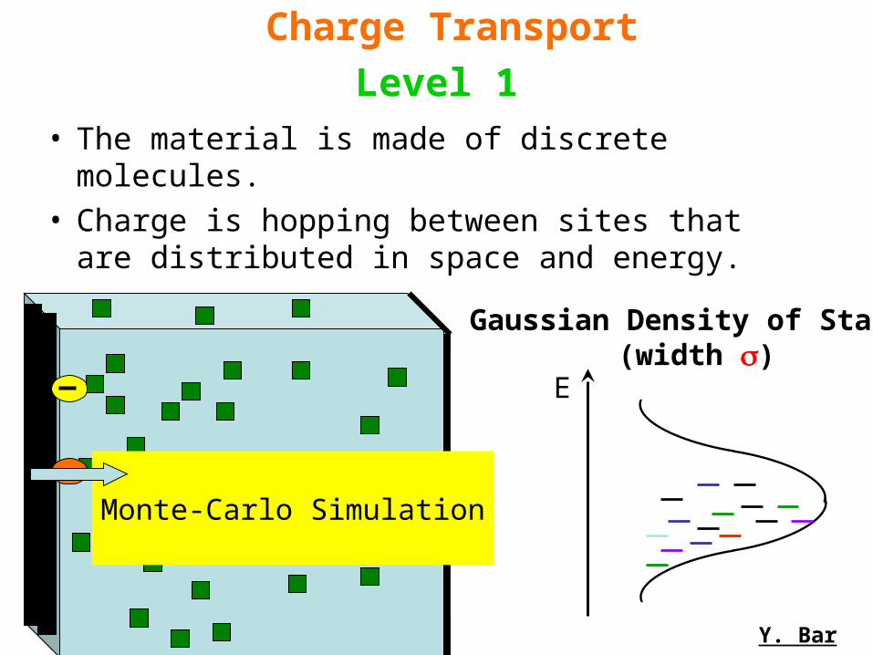
Level 1
• The material is made of discrete molecules.• Charge is hopping between sites that are
distributed in space and energy.
Charge Transport
Monte-Carlo Simulation
Gaussian Density of States(width )
E
Y. Bar


What do we extract from it?
• Can we apply statistics to describe the motion.
• Can we use Fermi-Dirac Statistics?
• Can we define a quasi-equilibrium?
Can we use the notion of: mobility () diffusivity (D)
If yes we can use/create device models
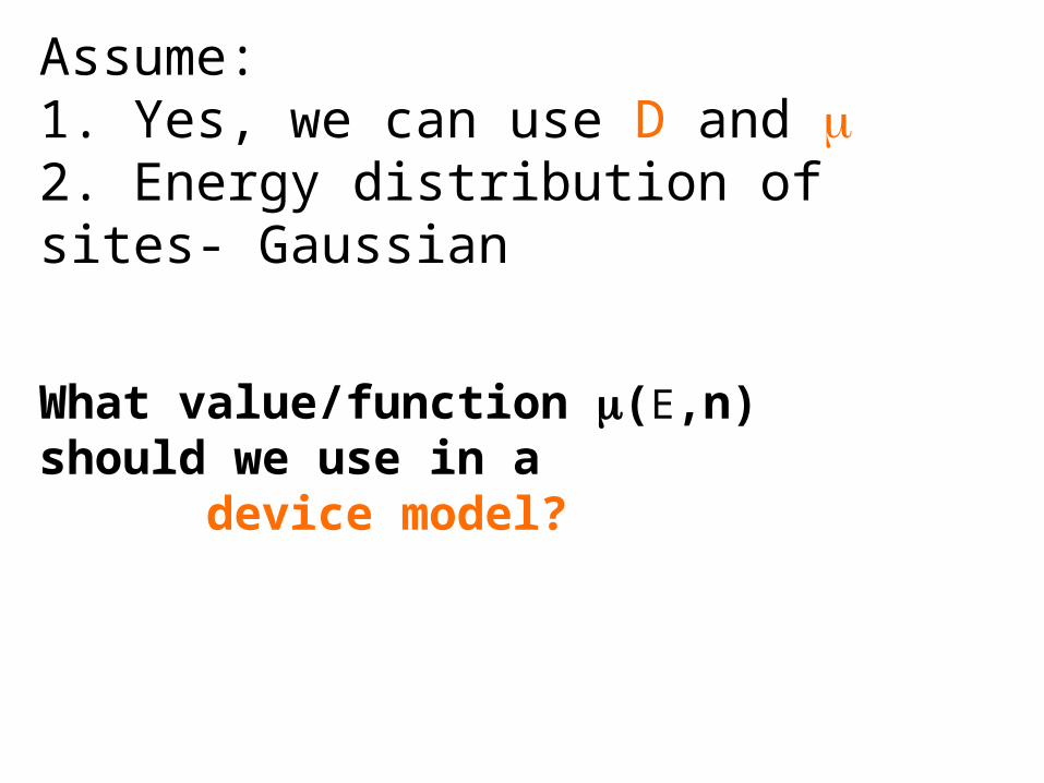
Assume:1. Yes, we can use D and 2. Energy distribution of sites- Gaussian
What value/function (E,n) should we use in a device model?
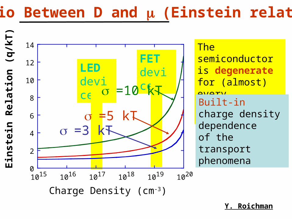
Ratio Between D and (Einstein relation)
The semiconductor is degenerate for (almost) every practical density
Built-in charge density dependence of the transport phenomena
LED device
FET device
0
2
4
6
8
10
12
14
10 10 10 10 10 1015 16 17 18 19 20
Charge Density (cm-3)
Ein
stei
n R
elat
ion
(q
/kT
)
=10 kT
=5 kT=3 kT
Y. Roichman

Use the Physical picture to study A very practical problem
HOMO Level(Valence “band”)
LUMO Level(Conduction)
Metal
Energy
E
Standard text book Model :
kT
E
e

Contact region Bulk region
x
Hot carriers thermalization
Cold carriers thermalization
Carriers diffusion at potential
Organic LED transport in the presence of energy disorder
B
Device Model of a contact region
3-10nm
Y. Preezant

The contact as simulated within a DEVICE model
Introducing the effect of the Einstein Relation Only
=4kT
=2kT
<<kT
Using text book analysis:
1. E is temperature dependent
2. Contact phenomena is unpredictable
1012
1013
1014
1015
1016
1017
1018
1019
1020
0 20 40 60 80 100
Ca
rrie
rs c
on
cen
tra
tio
n [
cm
-3]
Distance From Metalic Contact [nm]
Using the NEW model:
1. Good Agreement between Theory and Experiment
2. Contact phenomena is predictable
(As was shown on the poster)

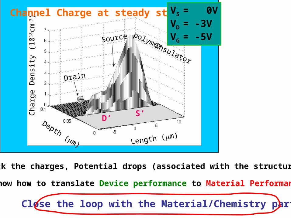
The contact phenomena(Through 2D modeling of Field Effect Transistor)
polymer
Cha
rge
Den
sity
(10
18cm
-3)
Insulator
Length (m)
Depth (m)
Drain Source
S’D’
t=t
D’ S’
Cha
rge
Den
sity
(10
18cm
-3)
Length (m)
Depth (m)
polymer Insulator
Drain
Source
Channel Charge at steady state VS = 0VVD = -3VVG = -5V
D’S’
Track the charges, Potential drops (associated with the structure), ….
Know how to translate Device performance to Material Performance
Close the loop with the Material/Chemistry part

Chemistry/Materials
Device Modeling
Device Design & measure
Analysis and extraction ofproperties
New Functionalities Novel Materials

Thanks To
Yoav EichenShay Tal
Uri BaninMiri KazesShi-hi Kan
Vlad MedvedevYevgeni PreezantYhoram BarYohai RoichmanNoam RapaportOlga SolomeshchAlexey RazinYair GanotSagi Shaked
Avecia Chemicals
Israel Science Foundation
European Union FW-6$