Embed Size (px)
Citation preview

Deirdre M. O’CarrollAssociate Professor
Rutgers UniversityDepartment of Materials Science and Engineering
Department of Chemistry and Chemical Biology
Group Website: http://photonics.rutgers.edu/ O’Carroll Lab
Organic, Hybrid and Low-Dimensional Semiconductors
for Electronic and Photonic Applications
http://photonics.rutgers.edu/

2
Non-Traditional Semiconductor Materials
Organic and Organic-Inorganic Hybrid Semiconductors
Examples: conjugated small molecules, conjugated polymers, hybrid perovskites, metal-oxide frameworks
Applications:
• wearable and flexible electronics,
• biosensors, bioimaging,
• thermal sensors,
• solar cells,
• photodetectors,
• light-emitting diodes.
Low-dimensional Semiconductors
Examples: graphene, transition metal dichalcogenides, nanowires, quantum dots, MXenes, black phosphorous
Applications:
• high-performance transistors,
• flexible electronics, transparent electrodes,
• supercapacitors,
• light-emitting diodes,
• IR photodetectors,
• quantum photonic and electronic devices.
Deirdre O’Carroll

Organic light emitting diodes (OLED) from Samsung & Philips
Organic Semiconductors
• Global market for products such as
organic light emitting displays, solar cells
and thin film transistors is forecast to be
more than $150 billion by 2027.†
• Trade-off between low mobility charge
carriers and exciton formation/dissociation.
† Global Organic Electronic Market, by Market Research Future
Organic
Semiconductors
Organic solar cells Thin film transistors (TFT)
• International companies using organic semiconductor materials (Samsung, Sony, IBM, Philips, LG…..)
• Motivation:
- Processing advantage of plastics,
- Synthetic tuneability,
- Frenkel-type excitons,
- Recent commercial availability,
- Earth abundant constituent elements.
O’Carroll LabDeirdre O’Carroll 3

4
Organic Semiconductor Research Examples
Non-Fullerene Organic Solar Cells
Device costs P-OLEDs were between 3-
5 times cheaper than inorganic LED
devices, per unit area; operating costs
were similar.
Embodied energy was a factor of up to
95 less for P-OLED and yearly GHG
emissions were comparable.
C. M. Carter, et al., Journal of Cleaner Production
137, 1418-1431 (2016).
Assessment of OLEDs
Cui et al., National Science Review 7, pp1239-1246 (2020)
Sun et al., Joule 4, 407-419 (2020)
Deirdre O’Carroll

5
Organic-Inorganic Hybrid Semiconductors
Pedesseau et al, ACS Nano 10, 9776-9786 (2016)
“Why Perovskite Solar Cells are So Efficient”
Physics Today (2018)
Perovskite-silicon tandem solar cells now being commercialized with efficiency up to 29.5% (e.g., Oxford PV)
Deirdre O’Carroll

6
Hybrid Semiconductor Research Examples
Nontoxic, Ultrastable CuI Hybrid LEDs
Zhu et al., ACS Energy Letters 6, pp 2565-2574 (2021)
Flexible InOx-Indicone Thin-film Transistors
Lee et al.,
Journal of Materials
Chemistry C
9, 4322 (2021)
Lin et al., Nature Energy 4, 864-873 (2019)
Tandem Hybrid Perovskite Solar Cells
Deirdre O’Carroll

7
Low-Dimensional Semiconductors
Fang et al., InfoMat 2, pp 291-317 (2020)Akinwande et al., Nature 573, p507 (2019)
Deirdre O’Carroll
Materials with nanometer confinement in one or more
dimensions: e.g., graphene, transition metal dichalcogenides,
nanowires, quantum dots, Mxenes, black phosphorous

8
Low-Dimensional Semiconductor Research Examples
Full-color Quantum Dot Photodetector Carbon Dots
Modified synthesisStandard synthesis
Carbon dots synthesized by solvothermal method
from 1,5-diaminonaphthalene and citric acid.
Javed, et al., Nanoscale Advances (2021)Kim et al., Science Advances 5 (2019)
Photodetectors based on PbS, CdSe
and CdS quantum dots
Deirdre O’Carroll
9
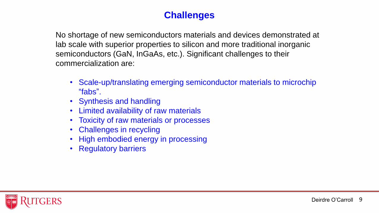
Challenges
No shortage of new semiconductors materials and devices demonstrated at
lab scale with superior properties to silicon and more traditional inorganic
semiconductors (GaN, InGaAs, etc.). Significant challenges to their
commercialization are:
• Scale-up/translating emerging semiconductor materials to microchip
“fabs”.
• Synthesis and handling
• Limited availability of raw materials
• Toxicity of raw materials or processes
• Challenges in recycling
• High embodied energy in processing
• Regulatory barriers
Deirdre O’Carroll

10
• Renewed focus on sustainability to avoid/mitigate pitfalls of resource hungry products.
• Improved avenues for early-stage researchers to converse with manufacturers and venture
capitalists to learn more about road-blocks to commercialization of semiconductor
materials.
• Factor cost, scale-up, raw materials supply alongside early-stage research into synthesis
and properties of new materials. Who does this? Retrain scientists, engineers,
entrepreneurs, product designers and developers?
• Develop better, more-assessible software to conduct life-cycle assessments, life-cycle
costing.
• Sustained investments in advanced manufacturing.
• Sustained investments in recycling of electronic and optoelectronic devices.
• Train/educate young scientists and engineers in how to assess the challenges of
commercialization.
Some Potential Solutions
Deirdre O’Carroll