Embed Size (px)
Citation preview
1
PhotovoltaicsPhotovoltaics and Photodetectors and Photodetectors -- part IIpart II
@ MITMarch 11, 2003 – Organic Optoelectronics - Lecture 10
• Organic Heterojunction Photovoltaic Cell
• Organic Multilayer Photodetector
Data on Solar Cells and Photodetectors taken from
Peumans, Bulovic, and Forrest., Appl. Phys. Lett. 76, 2650 (2000) – solar cell Appl. Phys. Lett. 76, 3855 (2000) - photodetector
2
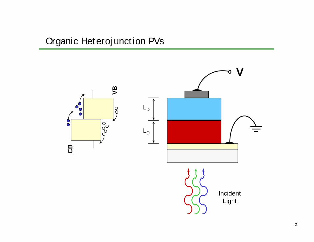
Organic Heterojunction PVs
CB
VBLD
LD
IncidentLight
V
3
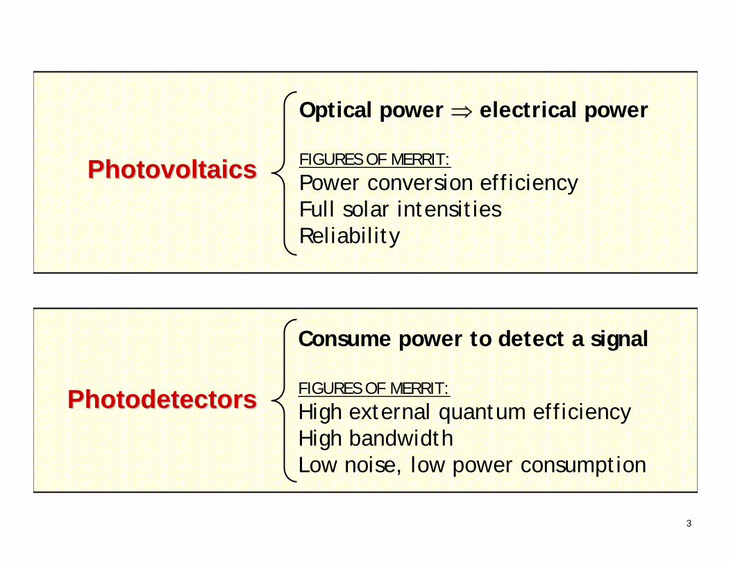
PhotovoltaicsPhotovoltaics
PhotodetectorsPhotodetectors
Optical power ⇒ electrical power
FIGURES OF MERRIT:
Power conversion efficiencyFull solar intensitiesReliability
Consume power to detect a signal
FIGURES OF MERRIT:
High external quantum efficiencyHigh bandwidthLow noise, low power consumption
4
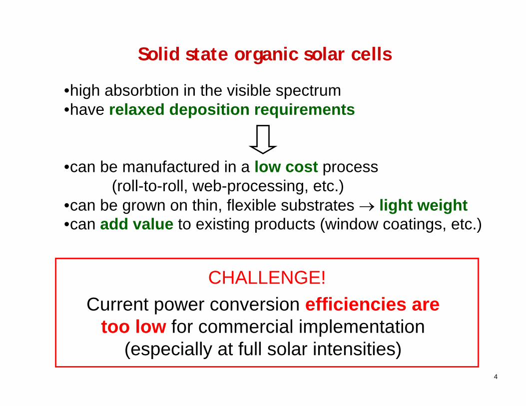
•high absorbtion in the visible spectrum•have relaxed deposition requirements
•can be manufactured in a low cost process (roll-to-roll, web-processing, etc.)
•can be grown on thin, flexible substrates → light weight•can add value to existing products (window coatings, etc.)
Solid state organic solar cells
CHALLENGE!Current power conversion efficiencies are
too low for commercial implementation (especially at full solar intensities)
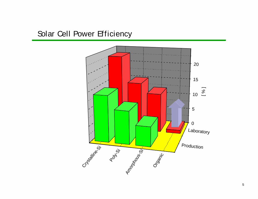
5
0
5
10
15
20
Laboratory
Production
Crystal
line-
Si
Poly-
Si
Amor
phou
s-Si
Orga
nic
[ % ]
Solar Cell Power Efficiency
6
VACUUMCHAMBER
TURBOPUMP
COLDTRAP
ROUGHINGPUMP
substrateholder
thicknessmonitor
shutter
GND
substrate
POWERSUPPLIES
sourceboats
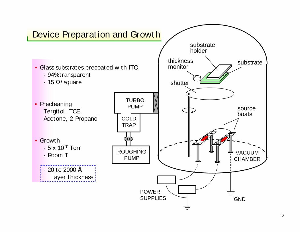
Device Preparation and Growth
• Glass substrates precoated with ITO- 94% transparent- 15 Ω/square
• PrecleaningTergitol, TCEAcetone, 2-Propanol
• Growth- 5 x 10⁻⁷ Torr- Room T
- 20 to 2000 Ålayer thickness
7
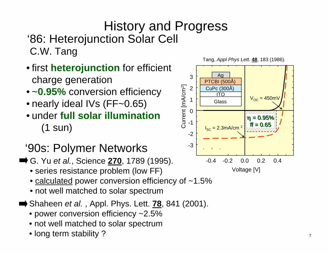
History and Progress ‘86: Heterojunction Solar Cell
• first heterojunction for efficient charge generation
• ~0.95% conversion efficiency• nearly ideal IVs (FF~0.65)• under full solar illumination
(1 sun)
‘90s: Polymer NetworksG. Yu et al., Science 270, 1789 (1995).• series resistance problem (low FF)• calculated power conversion efficiency of ~1.5%• not well matched to solar spectrumShaheen et al. , Appl. Phys. Lett. 78, 841 (2001).• power conversion efficiency ~2.5%• not well matched to solar spectrum• long term stability ?
C.W. Tang
η = 0.95%ff = 0.65η = 0.95%ff = 0.65
-0.4 -0.2 0.0 0.2 0.4
-3
-2
-1
0
1
2
3
Voltage [V]
Cur
rent
[mA
/cm
2 ]
ISC = 2.3mA/cm 2
VOC = 450mV
Tang, Appl Phys Lett. 48, 183 (1986).
CuPc (300Å)PTCBI (500Å)
GlassITO
Ag
8
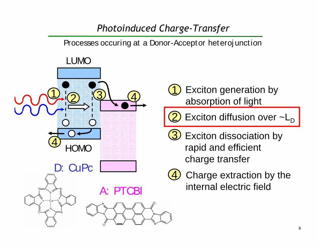
LUMO
HOMO
D: CuPc
A: PTCBI
2 3 4
4
Photoinduced Charge-Transfer
1
23
1 Exciton generation by absorption of light
4
Exciton diffusion over ~LD
Exciton dissociation by rapid and efficient charge transfer
Charge extraction by the internal electric field
Processes occuring at a Donor-Acceptor heterojunction
1 2 3 4
4
9
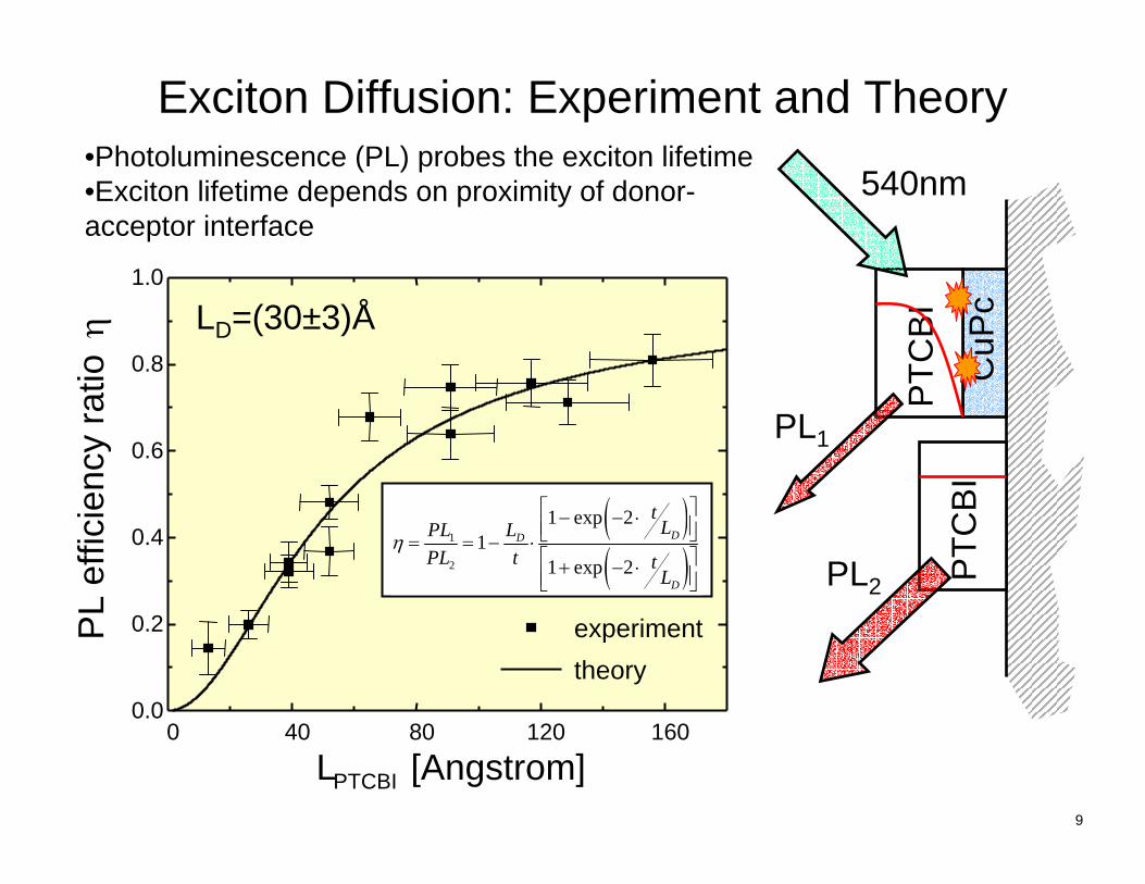
Exciton Diffusion: Experiment and Theory
0 40 80 120 1600.0
0.2
0.4
0.6
0.8
1.0
experimenttheory
PL
effic
ienc
y ra
tio η
LPTCBI [Angstrom]
CuP
cP
TCB
IP
TCB
I
540nm
PL1
PL2
( )( )
1
2
1 exp 21
1 exp 2
DD
D
tLPL L
PL t tL
η
⎡ ⎤− − ⋅⎢ ⎥⎣ ⎦= = − ⋅⎡ ⎤+ − ⋅⎢ ⎥⎣ ⎦
•Photoluminescence (PL) probes the exciton lifetime•Exciton lifetime depends on proximity of donor-acceptor interface
LD=(30±3)Å
10
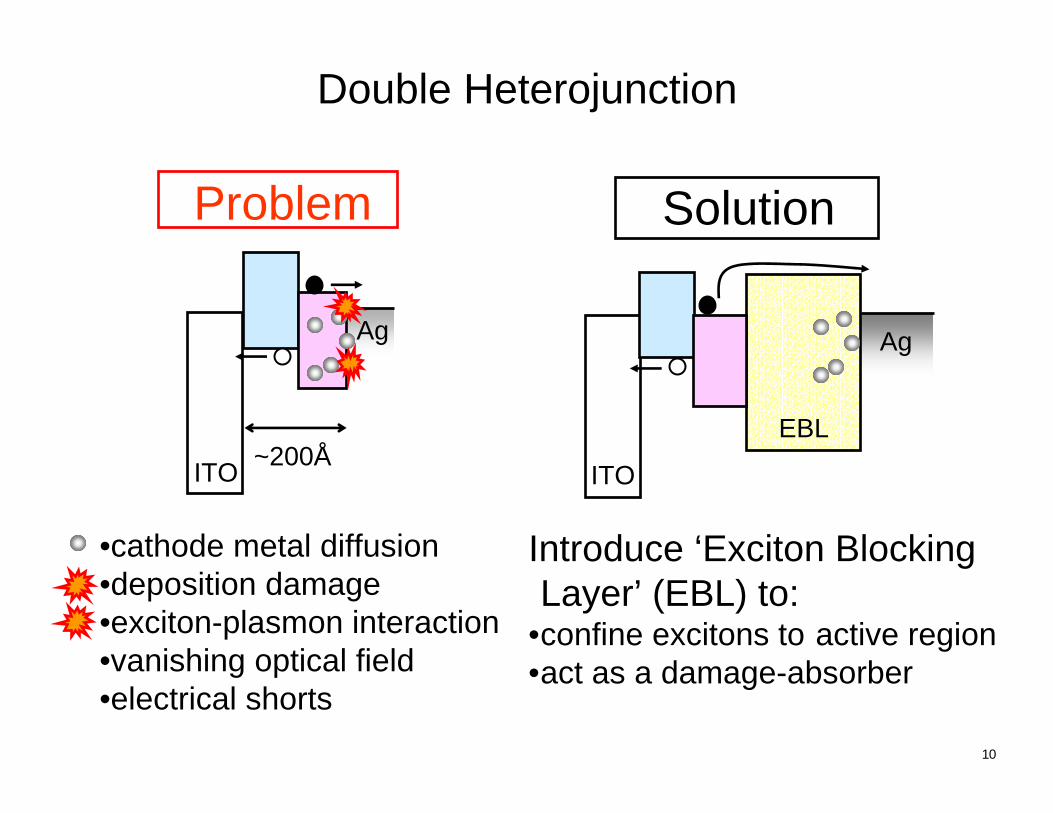
Double Heterojunction
Ag
Problem Solution
•cathode metal diffusion•deposition damage•exciton-plasmon interaction•vanishing optical field•electrical shorts
Introduce ‘Exciton Blocking Layer’ (EBL) to:
•confine excitons to active region•act as a damage-absorber
Ag
ITO ITO
EBL~200Å
11
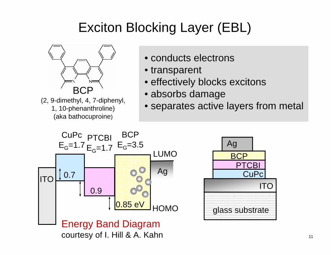
ITOCuPc
PTCBIBCP
Ag
glass substrate
Exciton Blocking Layer (EBL)
0.7
0.90.85 eV
CuPcEG=1.7
PTCBIEG=1.7
BCPEG=3.5
ITOAg
HOMO
LUMO
Energy Band Diagramcourtesy of I. Hill & A. Kahn
• conducts electrons• transparent• effectively blocks excitons• absorbs damage• separates active layers from metal
BCP(2, 9-dimethyl, 4, 7-diphenyl,
1, 10-phenanthroline)(aka bathocuproine)
12
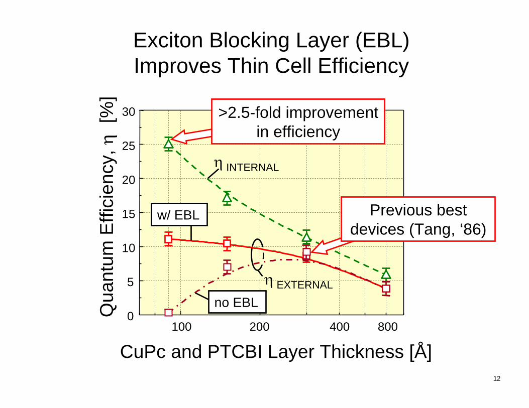
0
5
10
15
20
25
30
CuPc and PTCBI Layer Thickness [Å]
Qua
ntum
Effi
cien
cy, η
[%]
100 400200 800
η INTERNAL
η EXTERNAL
w/ EBL
no EBL
Exciton Blocking Layer (EBL)Improves Thin Cell Efficiency
>2.5-fold improvementin efficiency
Previous best devices (Tang, ‘86)
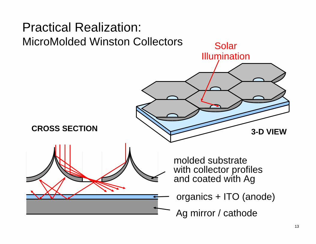
13
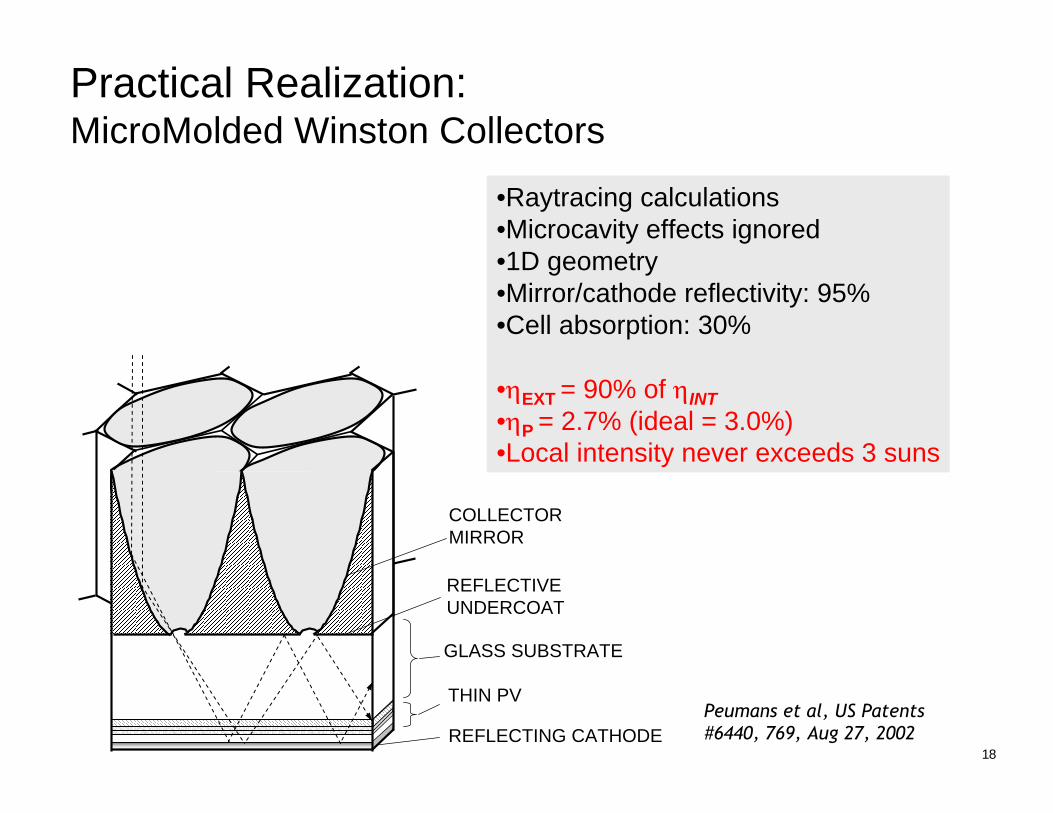
Ag mirror / cathode
organics + ITO (anode)
molded substrate with collector profiles and coated with Ag
SolarIllumination
CROSS SECTION 3-D VIEW
Practical Realization:MicroMolded Winston Collectors
14
400 600 800 10000
10
20
30
λ [nm]
0
2
4
Pho
ton
Flux
[101
8s-
1m
-2nm
-1]
1
3
Qua
ntum
Effi
cien
cy, η
[%]
η INTERNAL
AM1.5
η EXTERNAL
Solar Spectrum
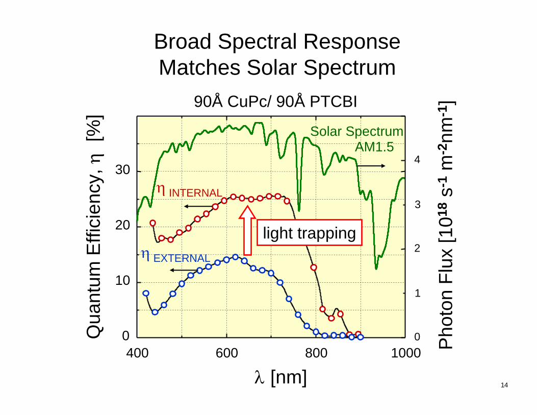
Broad Spectral ResponseMatches Solar Spectrum
light trapping
90Å CuPc/ 90Å PTCBI
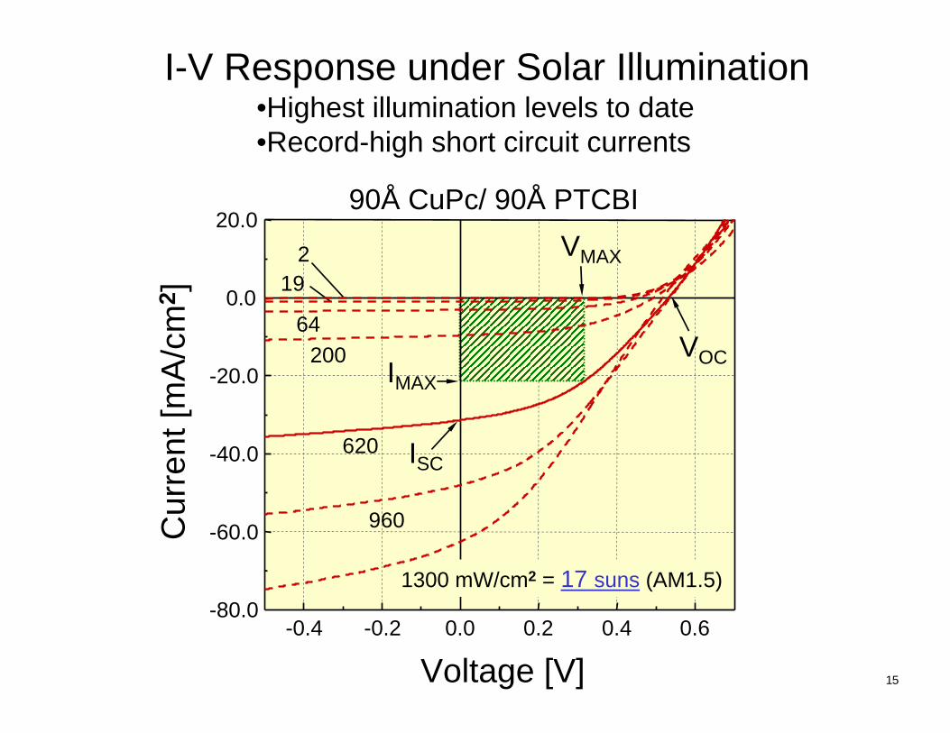
15
ISC
VOC
960
620
20064
192
-0.4 -0.2 0.0 0.2 0.4 0.6-80.0
-60.0
-40.0
-20.0
0.0
20.0
Voltage [V]
Cur
rent
[mA
/cm
2 ]
1300 mW/cm2 = 17 suns (AM1.5)
VMAX
IMAX
I-V Response under Solar Illumination•Highest illumination levels to date•Record-high short circuit currents
90Å CuPc/ 90Å PTCBI
16
I SC
[mA
/cm
2 ]
110
100
0.4
0.5
0.6
VO
C[V
]
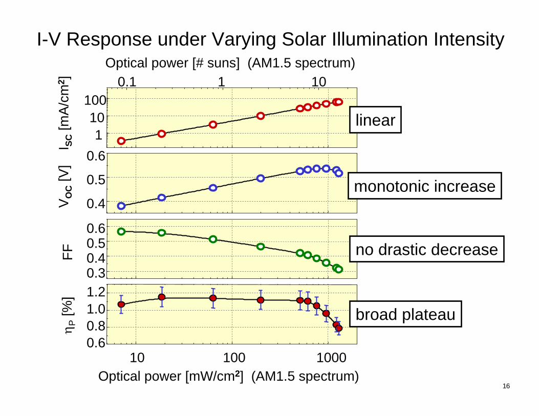
10 100 10000.60.81.01.2
Optical power [# suns] (AM1.5 spectrum)
Optical power [mW/cm2] (AM1.5 spectrum)
η P[%
]
0.30.40.50.6
FF0.1 1 10
I-V Response under Varying Solar Illumination Intensity
linear
monotonic increase
broad plateau
no drastic decrease
17
1 10 100 10000.0
0.5
1.0
1.5
2.0
2.5
3.0
no light trapping
w/ light trapping
Optical power [mW/cm2]
Pow
er C
onve
rsio
n E
ffici
ency
[%]
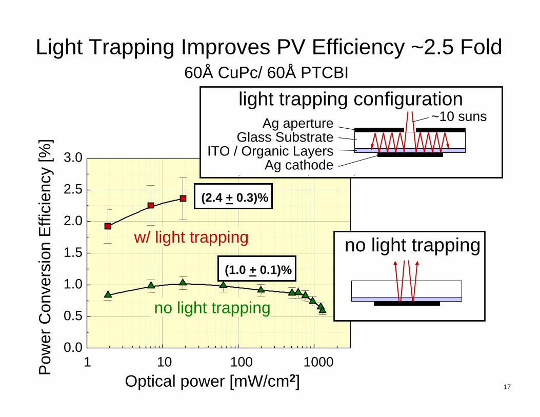
(2.4 + 0.3)%
Ag apertureGlass Substrate
ITO / Organic LayersAg cathode
~10 suns
Light Trapping Improves PV Efficiency ~2.5 Fold
no light trapping
light trapping configuration
(1.0 + 0.1)%
60Å CuPc/ 60Å PTCBI
18REFLECTING CATHODE
COLLECTORMIRROR
REFLECTIVEUNDERCOAT
THIN PV
GLASS SUBSTRATE
Practical Realization:MicroMolded Winston Collectors
•Raytracing calculations•Microcavity effects ignored•1D geometry•Mirror/cathode reflectivity: 95%•Cell absorption: 30%
•ηEXT = 90% of ηINT•ηP = 2.7% (ideal = 3.0%)•Local intensity never exceeds 3 suns
Peumans et al, US Patents #6440, 769, Aug 27, 2002
19
HEAT
PRESSURE
MOLD
SUPPORT
POLYMER
SHAPEDPOLYMERIC FILM
Collector Fabrication
100-
200µ
m
100-200µm
Peumans et al, US Patents #6440, 769, Aug 27, 2002
20
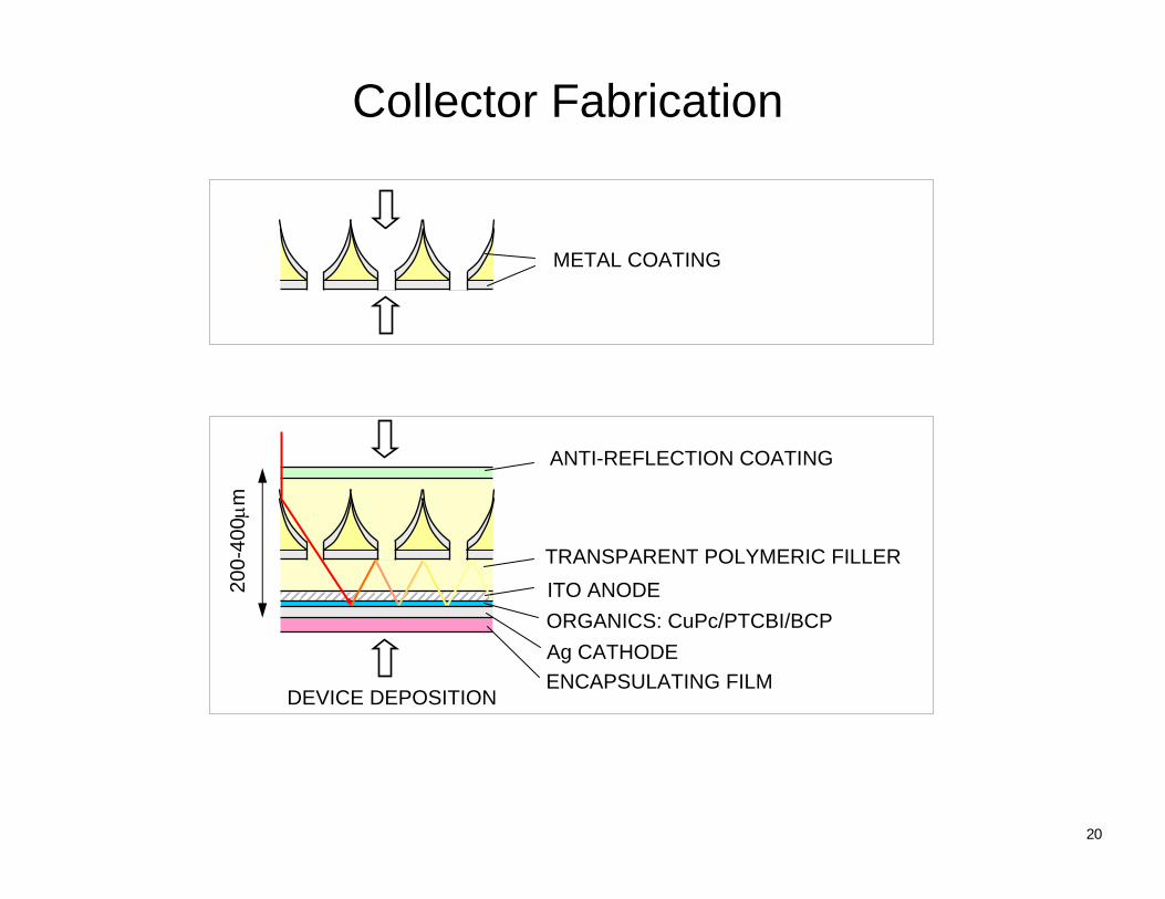
METAL COATING
ANTI-REFLECTION COATING
DEVICE DEPOSITION
TRANSPARENT POLYMERIC FILLERITO ANODEORGANICS: CuPc/PTCBI/BCPAg CATHODE
200-
400µ
m
ENCAPSULATING FILM
Collector Fabrication
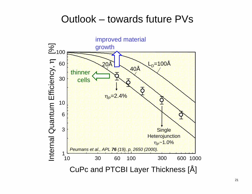
21
10 100 10001
100
CuPc and PTCBI Layer Thickness [Å]
Inte
rnal
Qua
ntum
Effi
cien
cy, η
[%]
30 60 300 600
30
60 LD=100Å40Å
20Å
ηP=2.4%
SingleHeterojunction
ηP~1.0%
10
3
6
improved materialgrowth
thinnercells
Outlook – towards future PVs
Peumans et al., APL 76 (19), p. 2650 (2000).
22
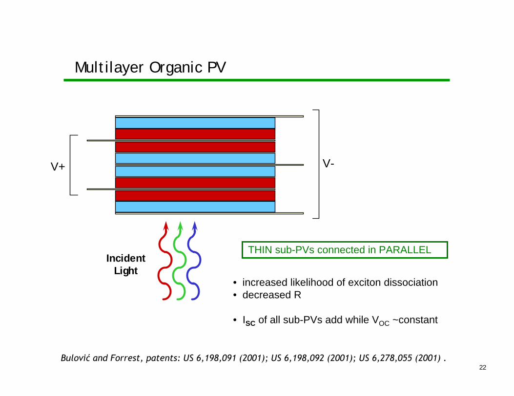
Multilayer Organic PV
IncidentLight
V+ V-
Bulović and Forrest, patents: US 6,198,091 (2001); US 6,198,092 (2001); US 6,278,055 (2001) .
THIN sub-PVs connected in PARALLEL
• increased likelihood of exciton dissociation• decreased R
• ISC of all sub-PVs add while VOC ~constant
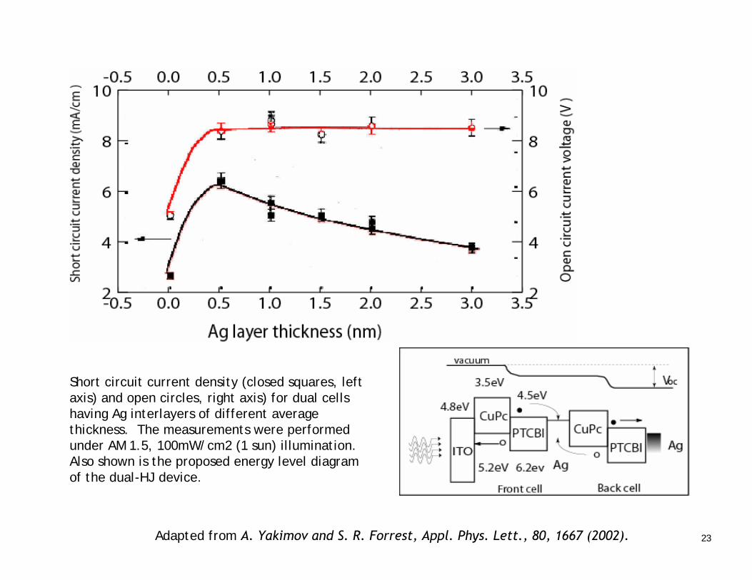
23Adapted from A. Yakimov and S. R. Forrest, Appl. Phys. Lett., 80, 1667 (2002).
Short circuit current density (closed squares, left axis) and open circles, right axis) for dual cells having Ag interlayers of different average thickness. The measurements were performed under AM 1.5, 100mW/cm2 (1 sun) illumination. Also shown is the proposed energy level diagram of the dual-HJ device.
24A. Yakimov and S. R. Forrest, Appl. Phys. Lett., 80, 1667 (2002).
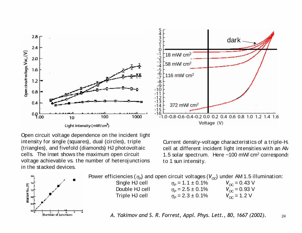
Power efficiencies (ηP) and open circuit voltages (VOC) under AM 1.5 illumination:Single HJ cell ηP = 1.1 ± 0.1% VOC = 0.43 VDouble HJ cell ηP = 2.5 ± 0.1% VOC = 0.93 VTriple HJ cell ηP = 2.3 ± 0.1% VOC = 1.2 V
Open circuit voltage dependence on the incident light intensity for single (squares), dual (circles), triple (triangles), and fivefold (diamonds) HJ photovoltaic cells. The inset shows the maximum open circuit voltage achievable vs. the number of heterojunctionsin the stacked devices.
Current density-voltage characteristics of a triple-HJcell at different incident light intensities with an AM1.5 solar spectrum. Here ~100 mW/cm2 correspondsto 1 sun intensity.
18 mW/cm2
58 mW/cm2
116 mW/cm2
372 mW/cm2
dark
25
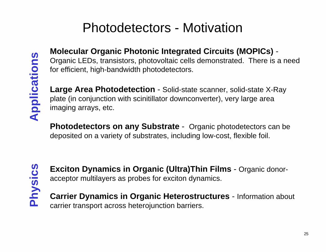
Photodetectors - MotivationMolecular Organic Photonic Integrated Circuits (MOPICs) -Organic LEDs, transistors, photovoltaic cells demonstrated. There is a needfor efficient, high-bandwidth photodetectors.
Large Area Photodetection - Solid-state scanner, solid-state X-Ray plate (in conjunction with scinitillator downconverter), very large area imaging arrays, etc.
Photodetectors on any Substrate - Organic photodetectors can be deposited on a variety of substrates, including low-cost, flexible foil.
App
licat
ions
Phys
ics Exciton Dynamics in Organic (Ultra)Thin Films - Organic donor-
acceptor multilayers as probes for exciton dynamics.
Carrier Dynamics in Organic Heterostructures - Information about carrier transport across heterojunction barriers.
26
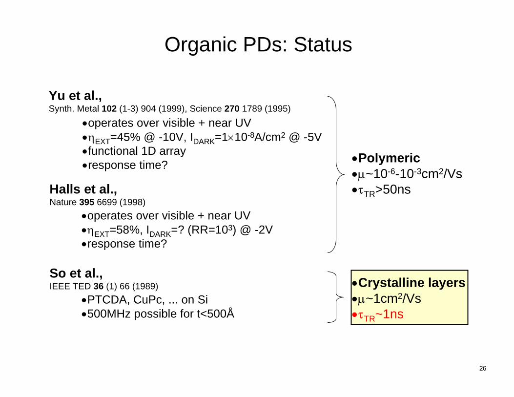
Organic PDs: Status
Yu et al.,Synth. Metal 102 (1-3) 904 (1999), Science 270 1789 (1995)
•operates over visible + near UV•ηEXT=45% @ -10V, IDARK=1×10⁻⁸A/cm2 @ -5V•functional 1D array•response time?
Halls et al.,Nature 395 6699 (1998)
•operates over visible + near UV•ηEXT=58%, IDARK=? (RR=103) @ -2V•response time?
So et al.,IEEE TED 36 (1) 66 (1989)
•PTCDA, CuPc, ... on Si•500MHz possible for t<500Å
•Polymeric•µ~10-6-10-3cm2/Vs•τTR>50ns
•Crystalline layers•µ~1cm2/Vs•τTR~1ns
27
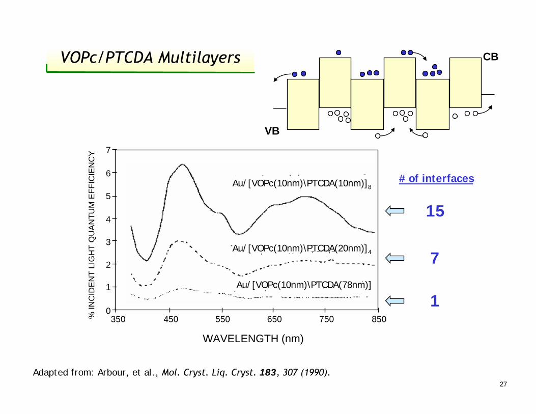
VOPc/PTCDA Multilayers
% IN
CID
EN
T LI
GH
T Q
UA
NTU
M E
FFIC
IEN
CY 7
6
5
4
3
2
1
0350 650450 550 750 850
WAVELENGTH (nm)
CB
VB
Adapted from: Arbour, et al., Mol. Cryst. Liq. Cryst. 183, 307 (1990).
# of interfaces
15
7
1
Au/[VOPc(10nm)\PTCDA(10nm)]8
Au/[VOPc(10nm)\PTCDA(20nm)]4
Au/[VOPc(10nm)\PTCDA(78nm)]
28
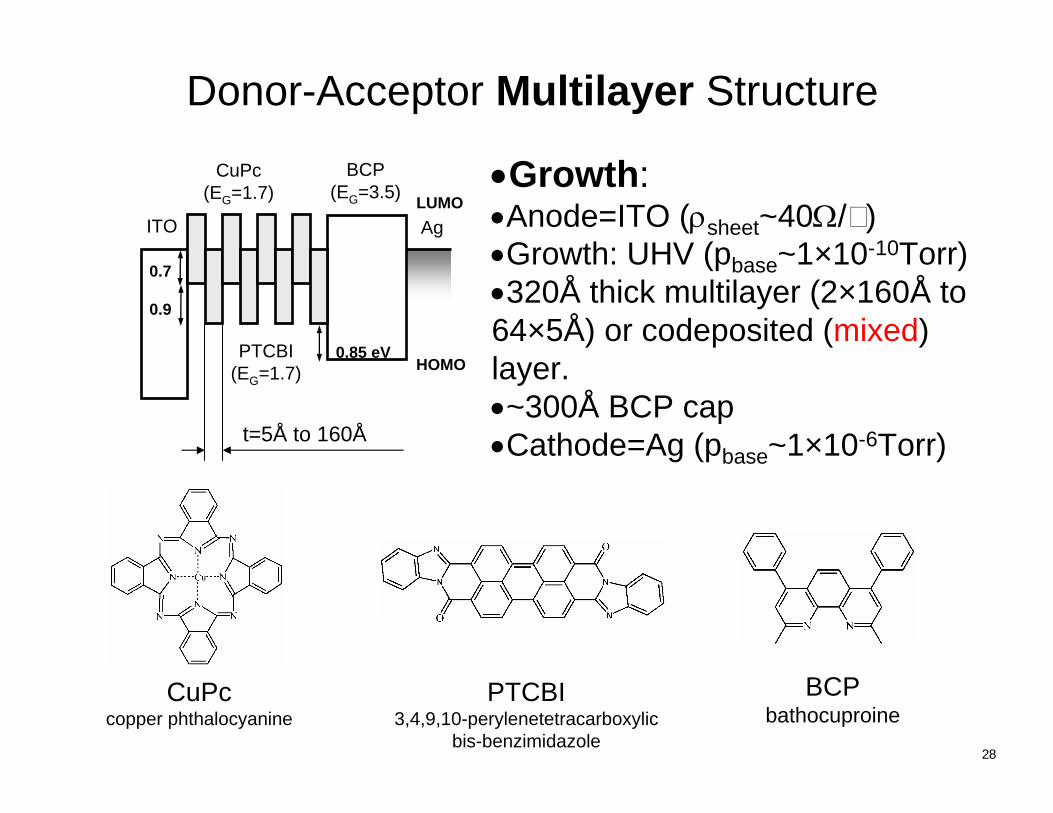
Donor-Acceptor Multilayer Structure
•Growth:•Anode=ITO (ρsheet~40Ω/ )•Growth: UHV (pbase~1×10⁻¹⁰Torr)•320Å thick multilayer (2×160Å to 64×5Å) or codeposited (mixed) layer.•~300Å BCP cap•Cathode=Ag (pbase~1×10⁻⁶Torr)
0.7
0.9
0.85 eVPTCBI(EG=1.7)
BCP(EG=3.5)
ITO AgLUMO
HOMO
CuPc(EG=1.7)
CuPccopper phthalocyanine
PTCBI3,4,9,10-perylenetetracarboxylic
bis-benzimidazole
BCPbathocuproine
t=5Å to 160Å
29
-10 -5 0 510-12
10-11
1x10⁻¹⁰
1x10⁻⁹
1x10⁻⁸
1x10⁻⁷
1x10⁻⁶
mixed10Å20Å80Å
t=160Å
Voltage [V]
Cur
rent
Den
sity
[A/c
m2 ]
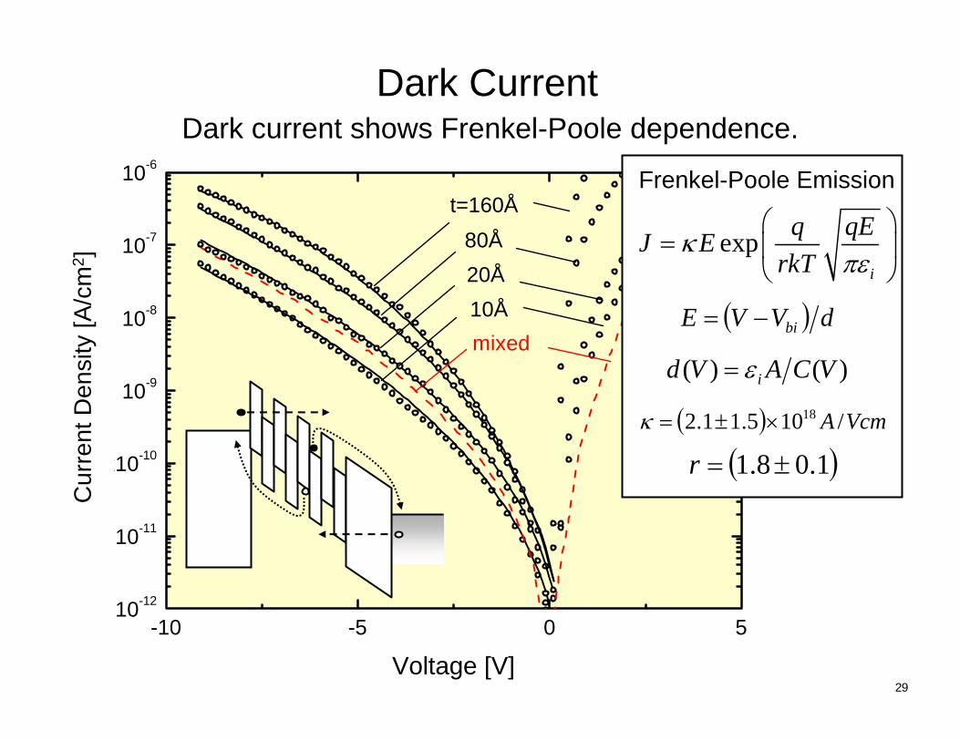
Dark Current
expi
q qEJ ErkT
κπε
⎛ ⎞= ⎜ ⎟
⎝ ⎠
( ) dVVE bi−=
( ) VcmA /105.11.2 18×±=κ
( )1.08.1 ±=r
Frenkel-Poole Emission
)()( VCAVd iε=
Dark current shows Frenkel-Poole dependence.
30
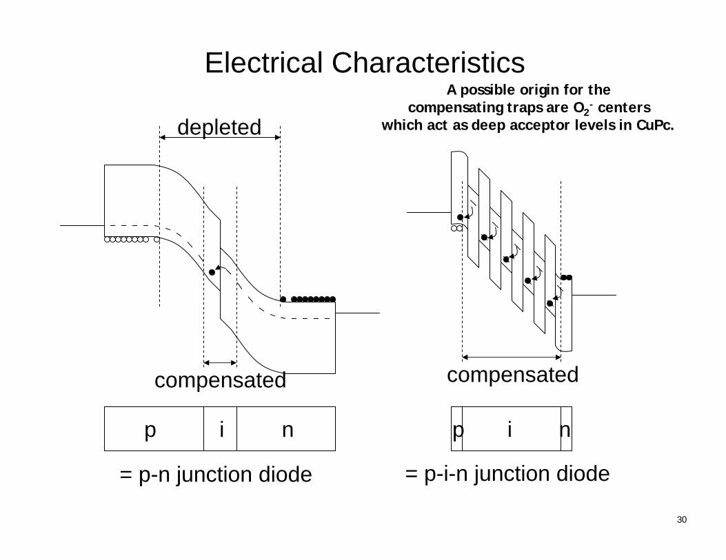
Electrical Characteristics
compensated
depleted
= p-n junction diode
compensated
p ni ip n
= p-i-n junction diode
A possible origin for thecompensating traps are O2
- centers which act as deep acceptor levels in CuPc.
31
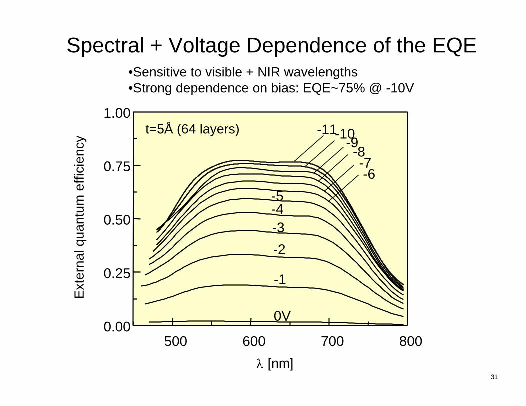
Spectral + Voltage Dependence of the EQE•Sensitive to visible + NIR wavelengths•Strong dependence on bias: EQE~75% @ -10V
500 600 700 8000.00
0.25
0.50
0.75
1.00-11-10-9-8
-7-6
-5-4-3-2
-1
0V
Ext
erna
l qua
ntum
effi
cien
cy
λ [nm]
t=5Å (64 layers)
32
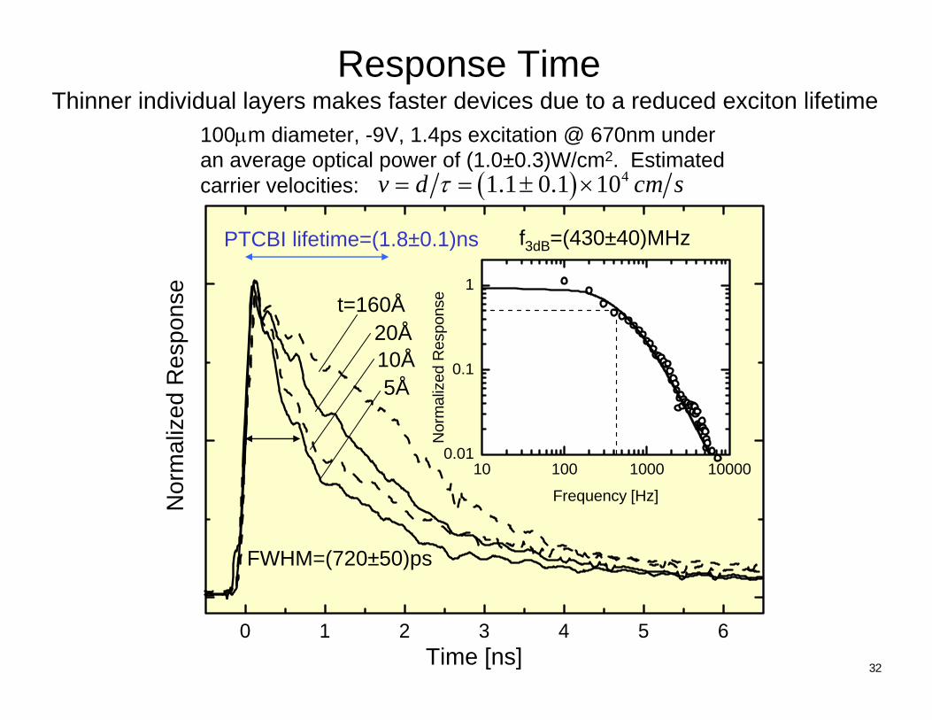
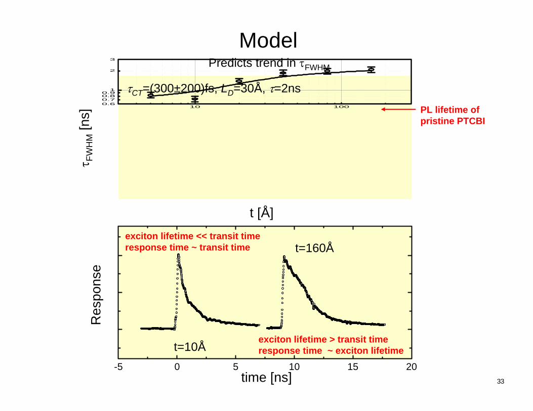
Response TimeThinner individual layers makes faster devices due to a reduced exciton lifetime
t=160Å20Å
5Å
0 1 2 3 4 5 6
Time [ns]
Nor
mal
ized
Res
pons
e
f3dB=(430±40)MHz
FWHM=(720±50)ps
10Å
10 100 1000 100000.01
0.1
1
Nor
mal
ized
Res
pons
e
Frequency [Hz]
PTCBI lifetime=(1.8±0.1)ns
100µm diameter, -9V, 1.4ps excitation @ 670nm under an average optical power of (1.0±0.3)W/cm2. Estimated carrier velocities: ( ) 41.1 0.1 10v d cm sτ= = ± ×
33
10 1000.60.70.80.9
1
2
3
-5 0 5 10 15 20
ModelPredicts trend in τFWHM
t=10Å
t=160Å
t [Å]
time [ns]
τ FW
HM
[ns]
Res
pons
e
exciton lifetime << transit timeresponse time ~ transit time
exciton lifetime > transit time response time ~ exciton lifetime
PL lifetime of pristine PTCBI
τCT=(300±200)fs, LD=30Å, τ=2ns