Embed Size (px)
Citation preview
Organic Electronic Devices Week 5: Organic Light-Emitting Devices and Emerging Technologies
Lecture 5.5: Course Review and Summary Bryan W. Boudouris Chemical Engineering Purdue University
1
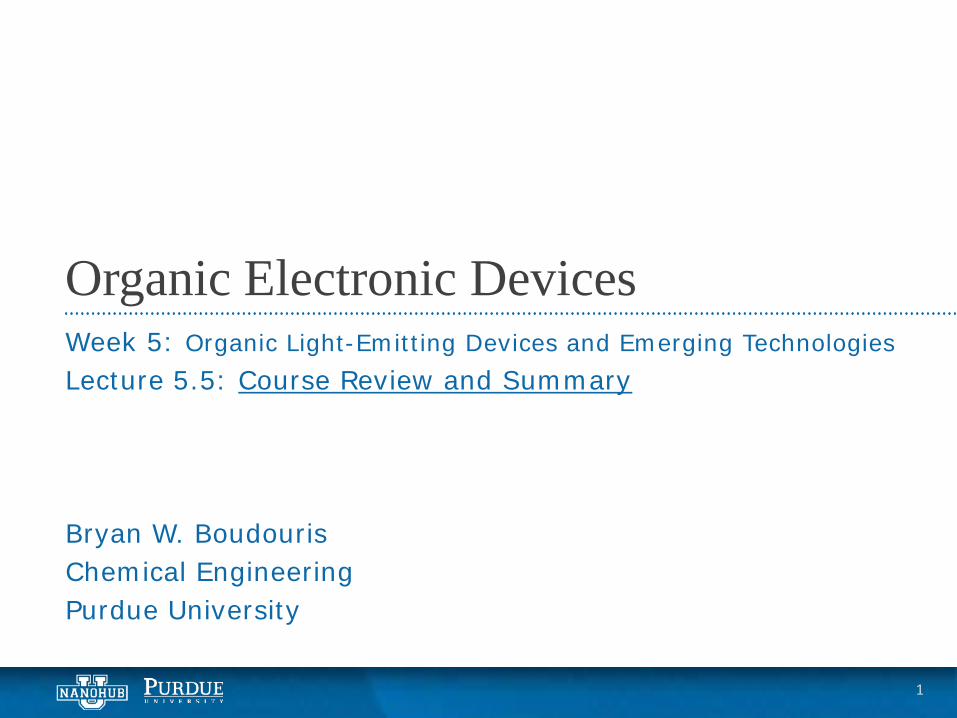
Understanding Device Operation Requires Knowledge of Materials
Sony
Organic Light-emitting Device (OLED) Displays Thin and Lightweight Flexible Transparent
Samsung Polytron
Organic Photovoltaic (OPV) Devices
Konarka Konarka Konarka
Large Area Production Portable Applications Conformal Coverage
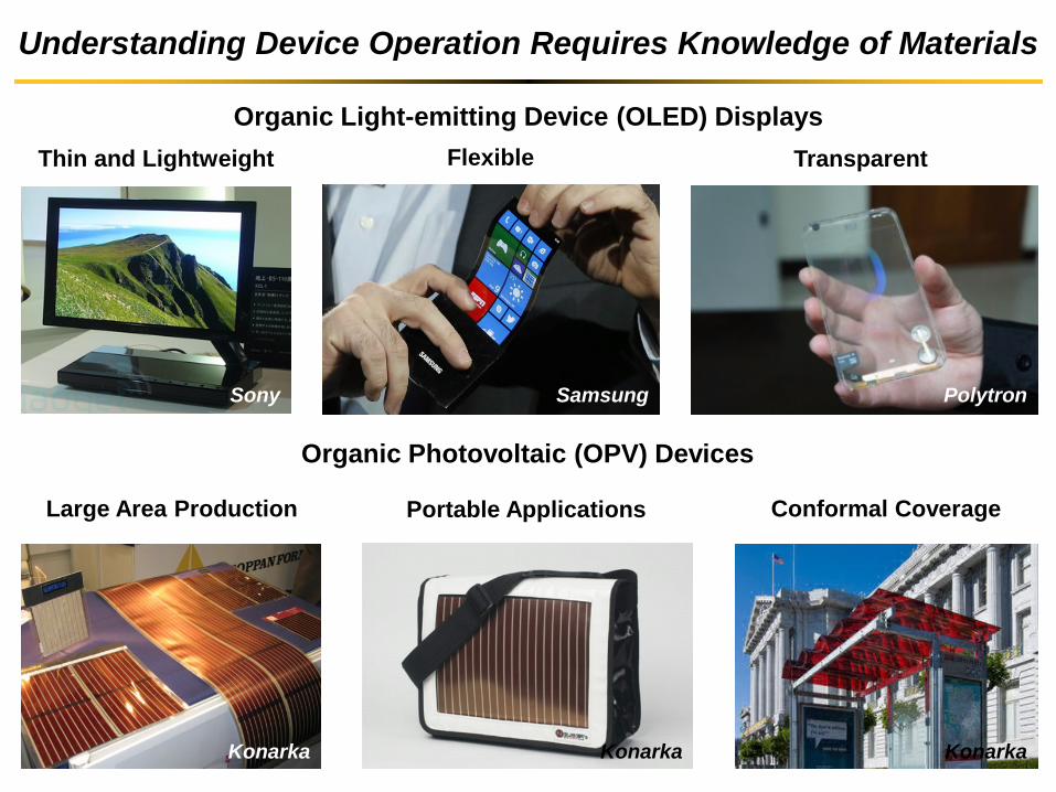
Commonly-used Polymeric Organic Semiconductors
P3AT
MEH-PPV
PDTP-DFBT PBDTTT-C PEDOT:PSS
Further Reading: Boudouris, B. W. Curr. Opin. Chem. Eng. 2013, 2, 294.
Primarily Hole Transporting (p-type) Polymer Semiconductors
Primarily Electron Transporting (n-type) Polymer Semiconductors
CN-MEH-PPV BBL P(NDI2OD-T2) PT01
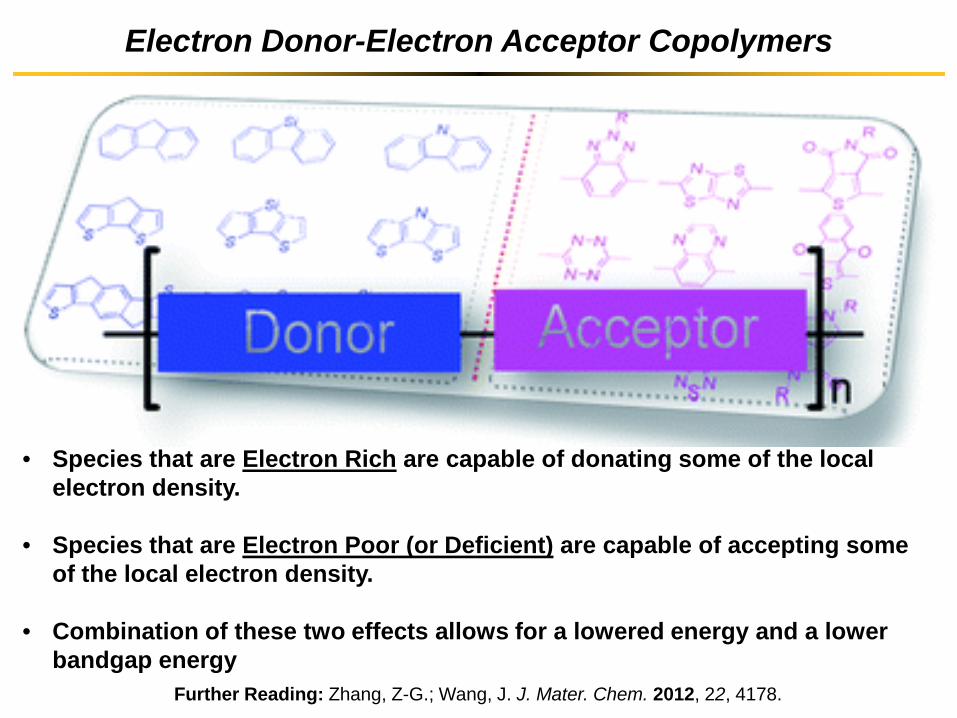
Electron Donor-Electron Acceptor Copolymers
Further Reading: Zhang, Z-G.; Wang, J. J. Mater. Chem. 2012, 22, 4178.
• Species that are Electron Rich are capable of donating some of the local electron density.
• Species that are Electron Poor (or Deficient) are capable of accepting some of the local electron density.
• Combination of these two effects allows for a lowered energy and a lower bandgap energy
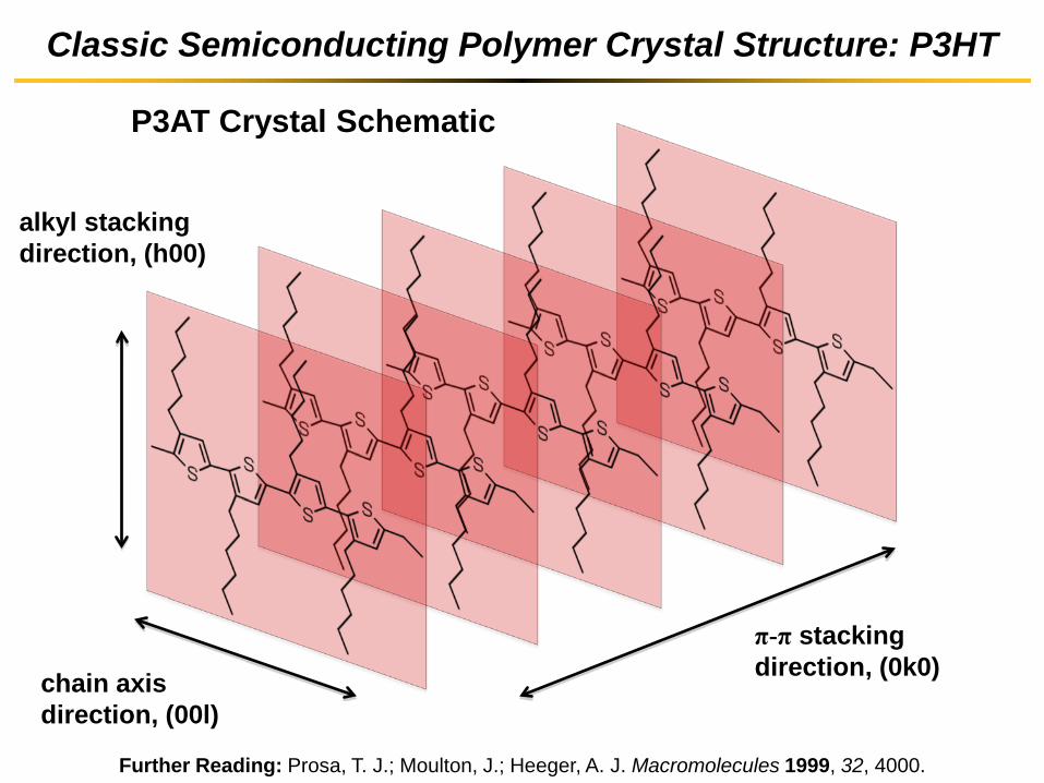
Classic Semiconducting Polymer Crystal Structure: P3HT
Further Reading: Prosa, T. J.; Moulton, J.; Heeger, A. J. Macromolecules 1999, 32, 4000.
π-π stacking direction, (0k0)
P3AT Crystal Schematic
chain axis direction, (00l)
alkyl stacking direction, (h00)
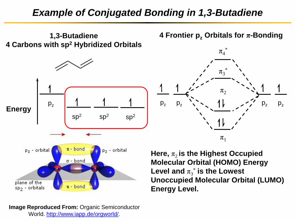
Example of Conjugated Bonding in 1,3-Butadiene
1,3-Butadiene 4 Carbons with sp2 Hybridized Orbitals
Energy pz
sp2 sp2 sp2
Image Reproduced From: Organic Semiconductor World. http://www.iapp.de/orgworld/.
4 Frontier pz Orbitals for π-Bonding
pz pz pz pz
π2
π1
π3*
π4*
Here, π2 is the Highest Occupied
Molecular Orbital (HOMO) Energy Level and π3
* is the Lowest Unoccupied Molecular Orbital (LUMO) Energy Level.
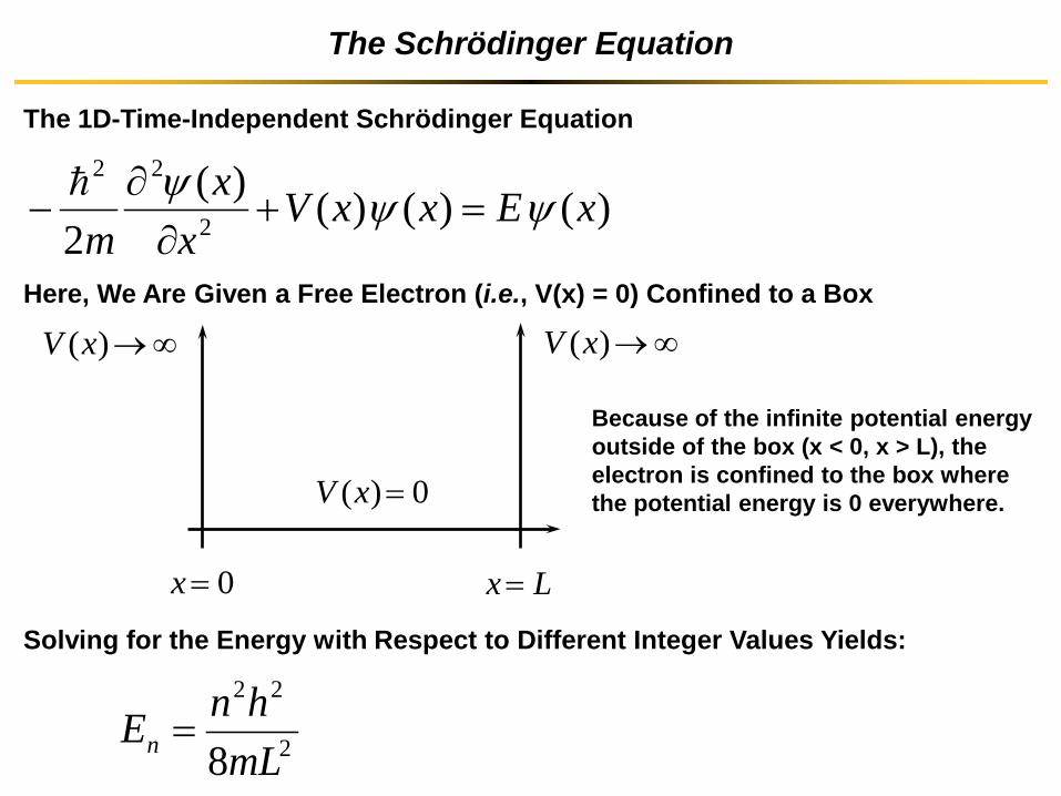
The Schrödinger Equation
The 1D-Time-Independent Schrödinger Equation
)()()()(2 2
22
xExxVx
xm
ψψψ=+
∂∂
−
Solving for the Energy with Respect to Different Integer Values Yields:
2
22
8mLhnEn =
Here, We Are Given a Free Electron (i.e., V(x) = 0) Confined to a Box
0)( =xV
∞→)(xV∞→)(xV
0=x Lx =
Because of the infinite potential energy outside of the box (x < 0, x > L), the electron is confined to the box where the potential energy is 0 everywhere.
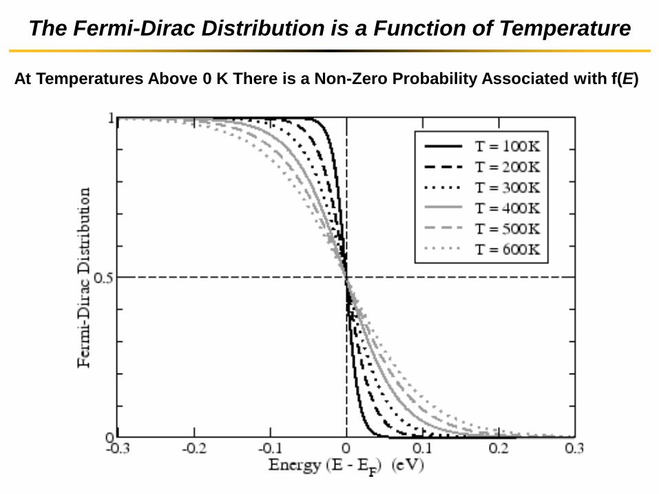
The Fermi-Dirac Distribution is a Function of Temperature
At Temperatures Above 0 K There is a Non-Zero Probability Associated with f(E)
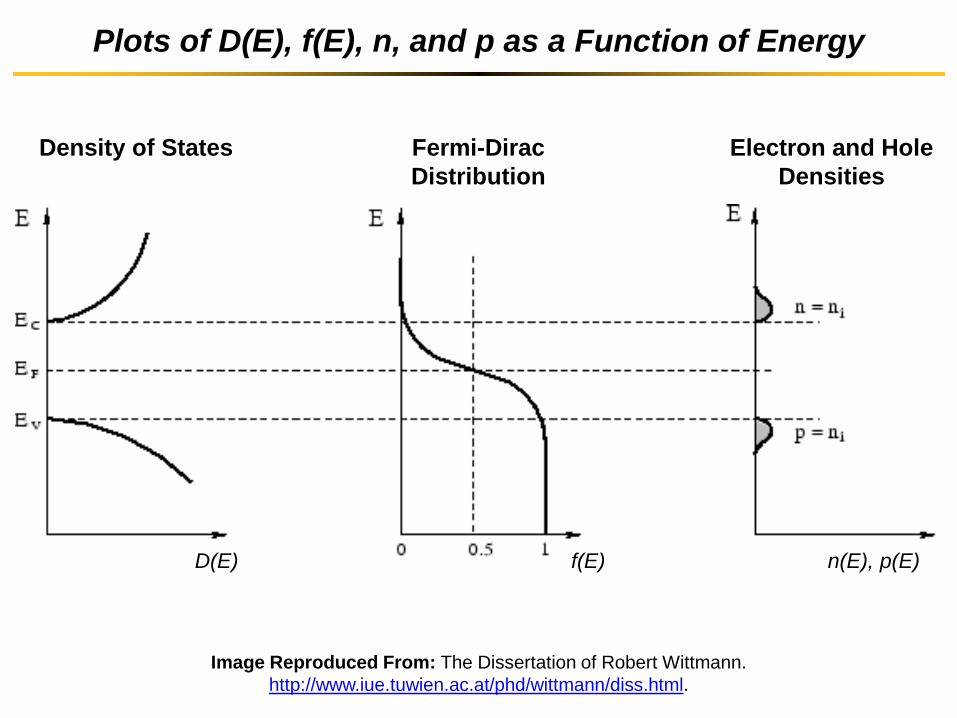
Plots of D(E), f(E), n, and p as a Function of Energy
D(E) f(E) n(E), p(E)
Density of States Fermi-Dirac Distribution
Electron and Hole Densities
Image Reproduced From: The Dissertation of Robert Wittmann. http://www.iue.tuwien.ac.at/phd/wittmann/diss.html.
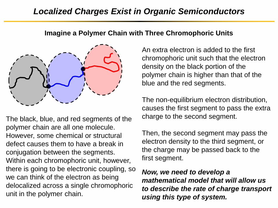
Localized Charges Exist in Organic Semiconductors
Imagine a Polymer Chain with Three Chromophoric Units
An extra electron is added to the first chromophoric unit such that the electron density on the black portion of the polymer chain is higher than that of the blue and the red segments. The non-equilibrium electron distribution, causes the first segment to pass the extra charge to the second segment. Then, the second segment may pass the electron density to the third segment, or the charge may be passed back to the first segment.
Now, we need to develop a mathematical model that will allow us to describe the rate of charge transport using this type of system.
The black, blue, and red segments of the polymer chain are all one molecule. However, some chemical or structural defect causes them to have a break in conjugation between the segments. Within each chromophoric unit, however, there is going to be electronic coupling, so we can think of the electron as being delocalized across a single chromophoric unit in the polymer chain.
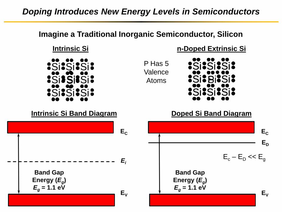
Doping Introduces New Energy Levels in Semiconductors
Imagine a Traditional Inorganic Semiconductor, Silicon
Si Si Si Si Si
Si Si Si Si
Si
Intrinsic Si
Intrinsic Si Band Diagram
EV
EC
Band Gap Energy (Eg) Eg = 1.1 eV
Ei
n-Doped Extrinsic Si
Si Si Si Si
Si Si Si Si
Si P Si Si Si
Si Si Si Si
Si
P Has 5 Valence Atoms
Doped Si Band Diagram
EV
EC
Band Gap Energy (Eg) Eg = 1.1 eV
ED
Ec – ED << Eg
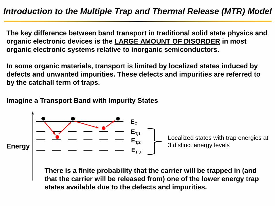
Introduction to the Multiple Trap and Thermal Release (MTR) Model
Imagine a Transport Band with Impurity States
The key difference between band transport in traditional solid state physics and organic electronic devices is the LARGE AMOUNT OF DISORDER in most organic electronic systems relative to inorganic semiconductors. In some organic materials, transport is limited by localized states induced by defects and unwanted impurities. These defects and impurities are referred to by the catchall term of traps.
Energy
EC
ET,1
ET,2
ET,3
Localized states with trap energies at 3 distinct energy levels
There is a finite probability that the carrier will be trapped in (and that the carrier will be released from) one of the lower energy trap states available due to the defects and impurities.
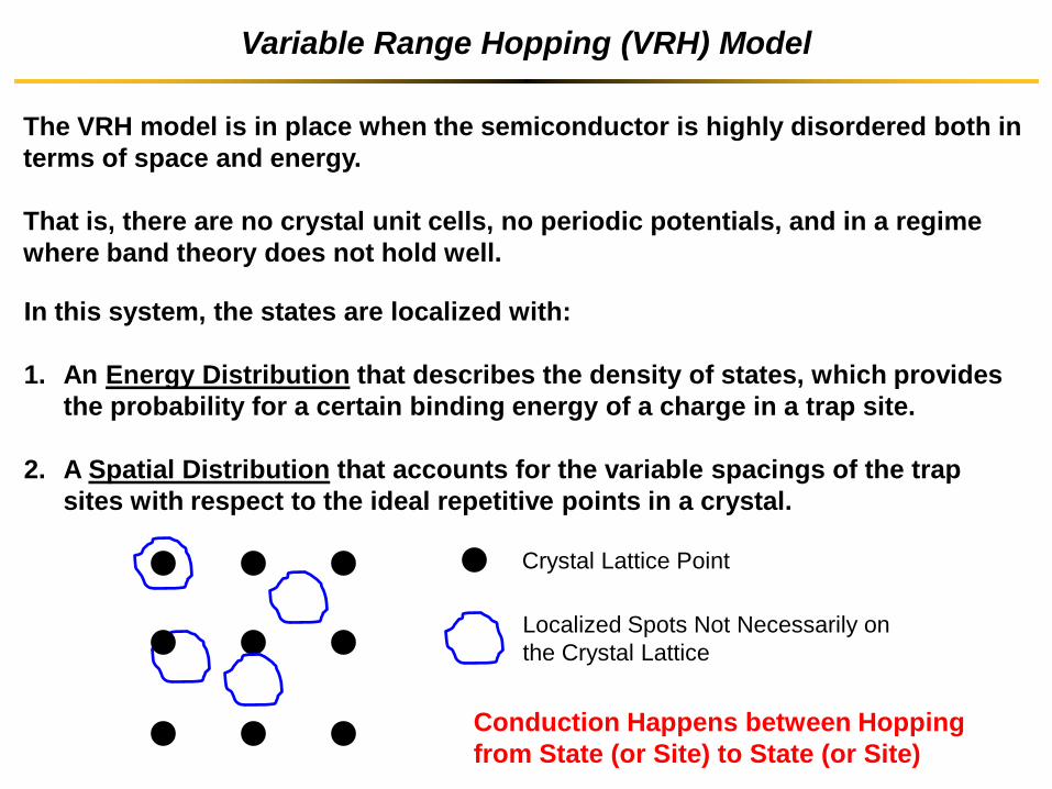
Variable Range Hopping (VRH) Model
The VRH model is in place when the semiconductor is highly disordered both in terms of space and energy. That is, there are no crystal unit cells, no periodic potentials, and in a regime where band theory does not hold well.
In this system, the states are localized with: 1. An Energy Distribution that describes the density of states, which provides
the probability for a certain binding energy of a charge in a trap site.
2. A Spatial Distribution that accounts for the variable spacings of the trap sites with respect to the ideal repetitive points in a crystal.
Crystal Lattice Point
Localized Spots Not Necessarily on the Crystal Lattice
Conduction Happens between Hopping from State (or Site) to State (or Site)
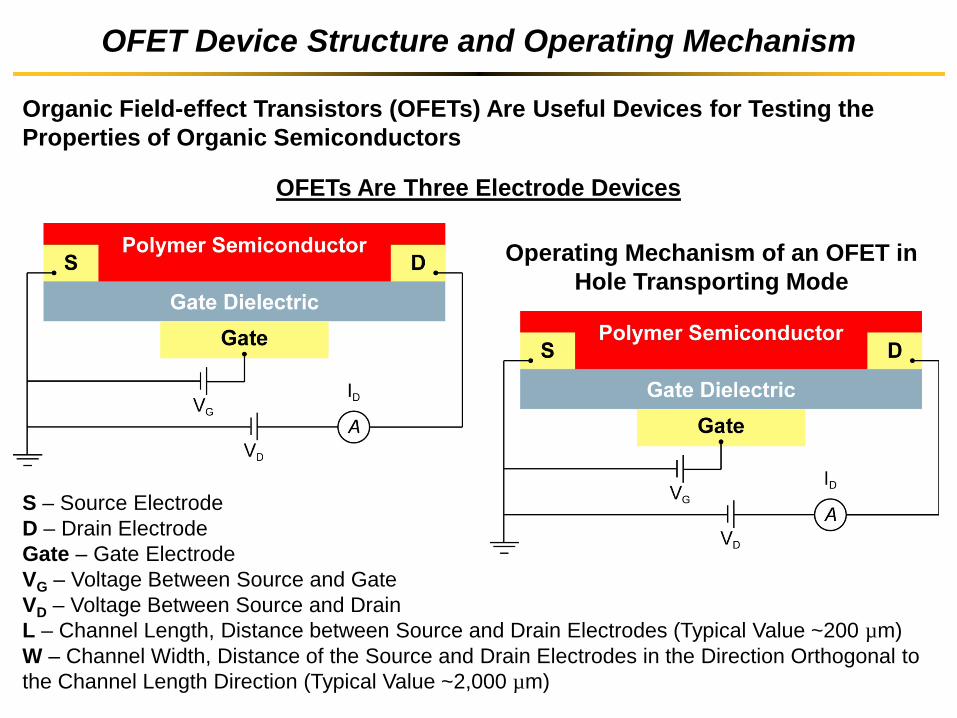
OFET Device Structure and Operating Mechanism
Organic Field-effect Transistors (OFETs) Are Useful Devices for Testing the Properties of Organic Semiconductors
OFETs Are Three Electrode Devices
S – Source Electrode D – Drain Electrode Gate – Gate Electrode VG – Voltage Between Source and Gate VD – Voltage Between Source and Drain L – Channel Length, Distance between Source and Drain Electrodes (Typical Value ~200 µm) W – Channel Width, Distance of the Source and Drain Electrodes in the Direction Orthogonal to the Channel Length Direction (Typical Value ~2,000 µm)
Operating Mechanism of an OFET in Hole Transporting Mode
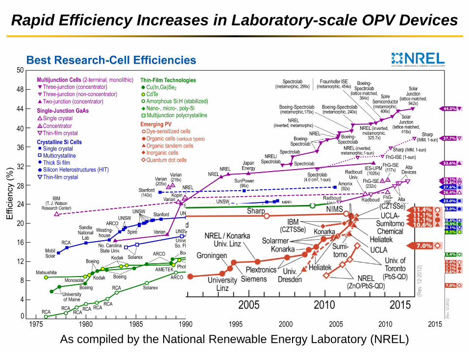
Rapid Efficiency Increases in Laboratory-scale OPV Devices
As compiled by the National Renewable Energy Laboratory (NREL)
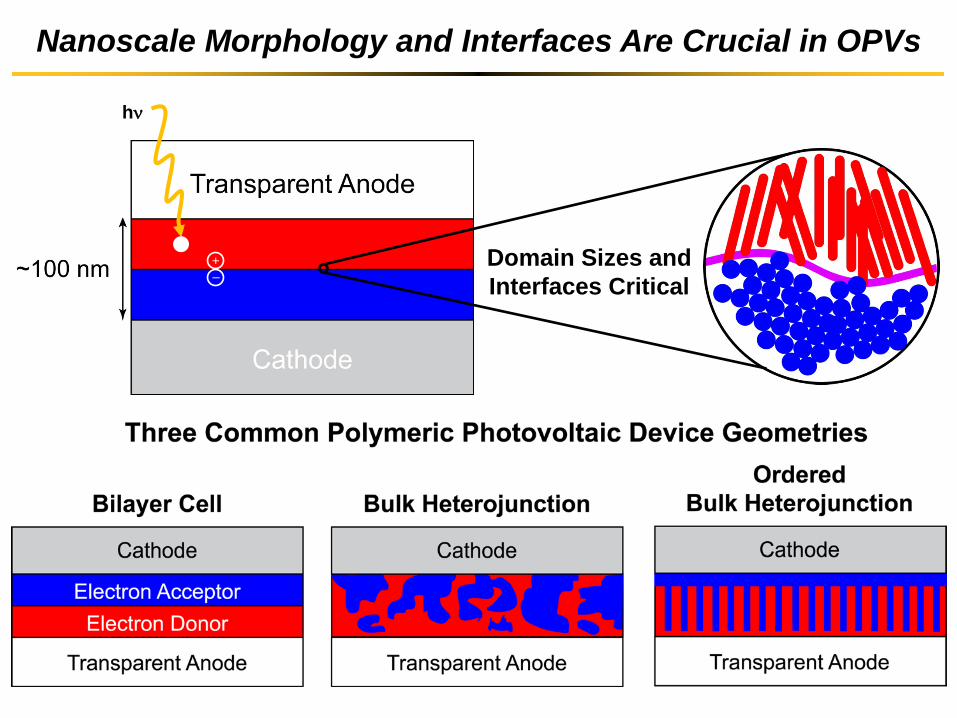
Domain Sizes and Interfaces Critical
+ –
hν
Nanoscale Morphology and Interfaces Are Crucial in OPVs
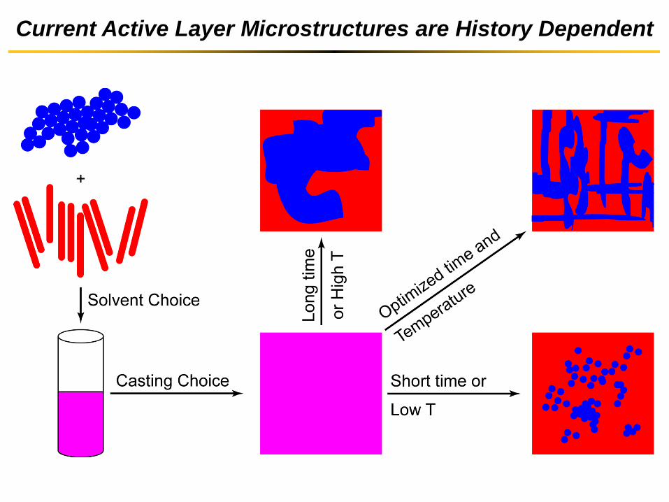
Current Active Layer Microstructures are History Dependent
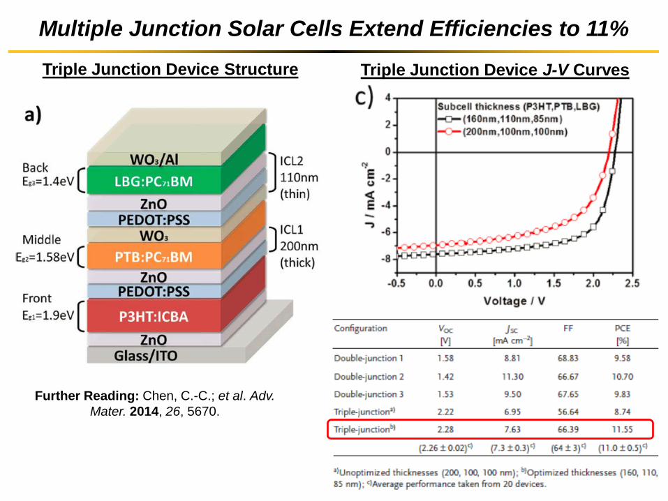
Multiple Junction Solar Cells Extend Efficiencies to 11%
Further Reading: Chen, C.-C.; et al. Adv. Mater. 2014, 26, 5670.
Triple Junction Device Structure Triple Junction Device J-V Curves
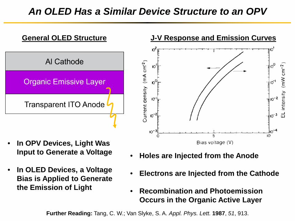
An OLED Has a Similar Device Structure to an OPV
Further Reading: Tang, C. W.; Van Slyke, S. A. Appl. Phys. Lett. 1987, 51, 913.
General OLED Structure J-V Response and Emission Curves
• In OPV Devices, Light Was Input to Generate a Voltage
• In OLED Devices, a Voltage Bias is Applied to Generate the Emission of Light
• Holes are Injected from the Anode
• Electrons are Injected from the Cathode
• Recombination and Photoemission Occurs in the Organic Active Layer
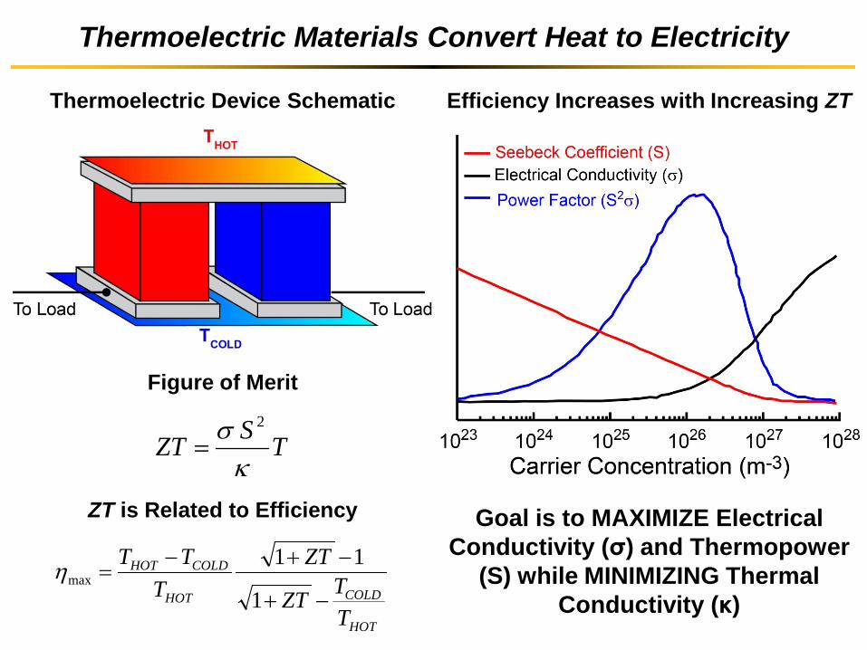
Thermoelectric Materials Convert Heat to Electricity
Thermoelectric Device Schematic
TSZTκ
σ 2
=
Figure of Merit
Goal is to MAXIMIZE Electrical Conductivity (σ) and Thermopower
(S) while MINIMIZING Thermal Conductivity (κ)
Efficiency Increases with Increasing ZT
HOT
COLDHOT
COLDHOT
TTZT
ZTT
TT
−+
−+−=
1
11maxη
ZT is Related to Efficiency
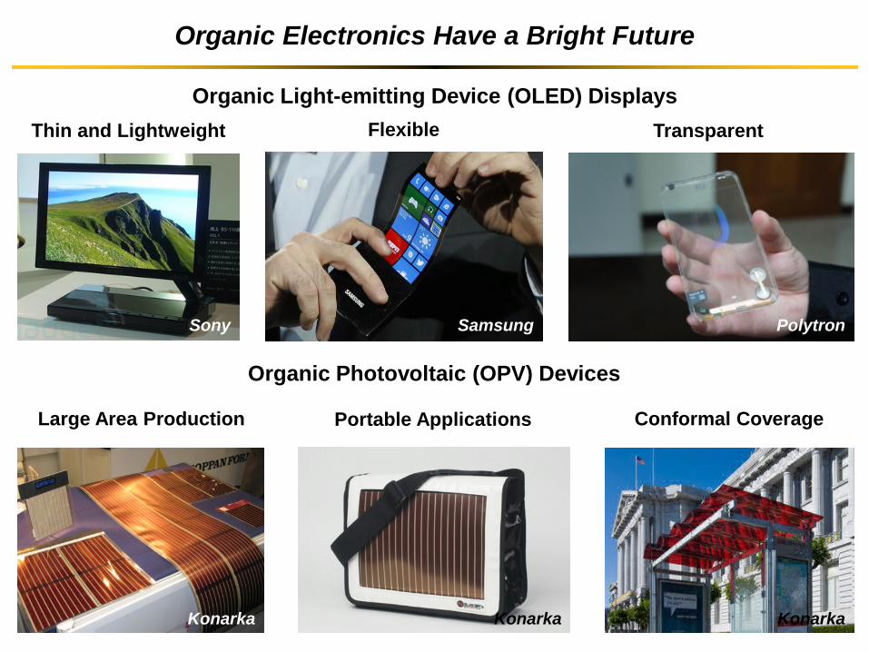
Organic Electronics Have a Bright Future
Sony
Organic Light-emitting Device (OLED) Displays Thin and Lightweight Flexible Transparent
Samsung Polytron
Organic Photovoltaic (OPV) Devices
Konarka Konarka Konarka
Large Area Production Portable Applications Conformal Coverage