Embed Size (px)
Citation preview
Organic and Molecular Electronics
Innovation in full bloom
Silylethyne-Substituted Pentacenes
Self-Assembled Nanodielectrics (SANDs) for Unconventional Electronics
Polytriarylamine Semiconductors
Organic Semiconductor Laser Materials
Electronics and Self-Assembly with Single Molecules
TM
Vol. 4, No. 3
Intr
oduc
tion
Aldrich Chemical Co., Inc. Sigma-Aldrich Corporation6000 N. Teutonia Ave.Milwaukee, WI 53209, USA
To Place OrdersTelephone 800-325-3010 (USA)FAX 800-325-5052 (USA)
Customer & Technical ServicesCustomer Inquiries 800-325-3010Technical Service 800-231-8327SAFC® 800-244-1173Custom Synthesis 800-244-1173Flavors & Fragrances 800-227-4563International 414-438-385024-Hour Emergency 414-438-3850Web site sigma-aldrich.comEmail [email protected]
SubscriptionsTo request your FREE subscription to Material Matters, please contact us by:
Phone: 800-325-3010 (USA)
Mail: Attn: Marketing Communications Aldrich Chemical Co., Inc. Sigma-Aldrich Corporation P.O. Box 2988 Milwaukee, WI 53201-2988
Website: sigma-aldrich.com/mm Email: [email protected]
International customers, please contact your local Sigma-Aldrich office. For worldwide contact information, please see back cover.
Material Matters is also available in PDF format on the Internet at sigma-aldrich.com/matsci.
Aldrich brand products are sold through Sigma-Aldrich, Inc. Sigma-Aldrich, Inc. warrants that its products conform to the information contained in this and other Sigma-Aldrich publications. Purchaser must determine the suitability of the product for its particular use. See reverse side of invoice or packing slip for additional terms and conditions of sale.
All prices are subject to change without notice.
Material Matters (ISSN 1933–9631) is a publication of Aldrich Chemical Co., Inc. Aldrich is a member of the Sigma-Aldrich Group. © 2009 Sigma-Aldrich Co.
TM
Vol. 4 No. 3
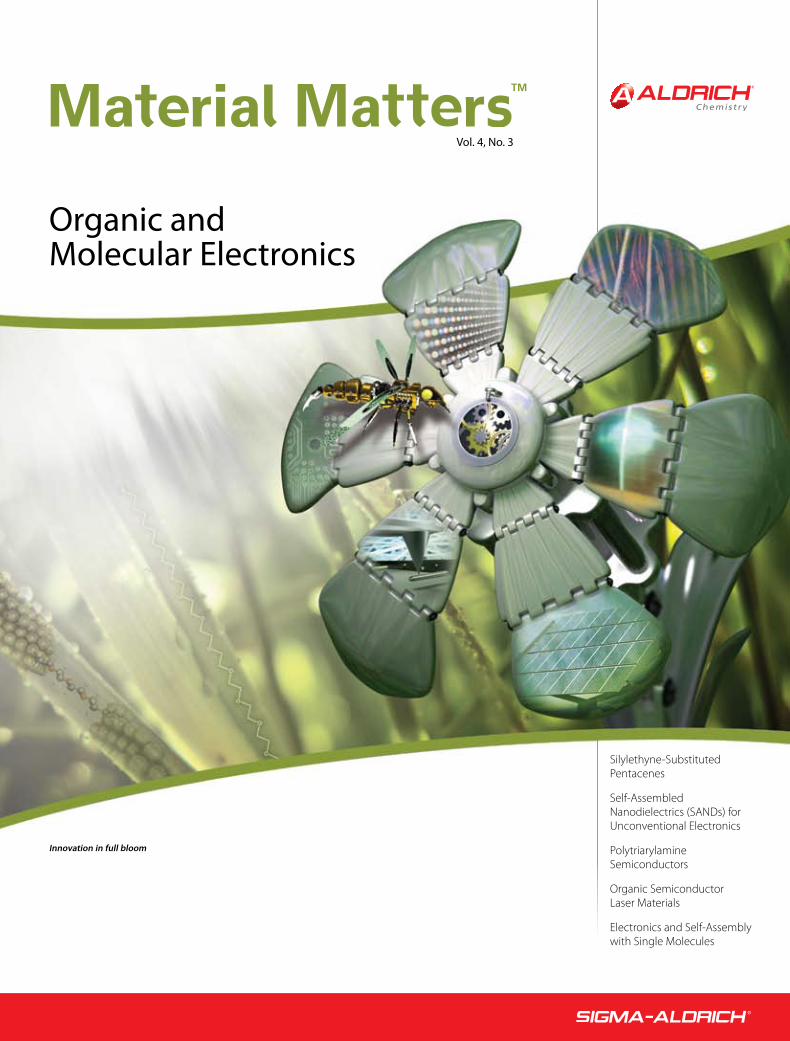
About Our CoverResearch in Organic and Molecular Electronics requires the exploration of the nanoscale realm whether it is to understand the bulk performance of molecules in devices or to create nanogaps in which a single molecule, held between two electrodes, can be studied. Examples of devices include low-cost flexible organic solar cell devices which can harvest photons from the sun. Here we show an artist’s rendition of the imagery associated with devices and materials of this field. The petals of the molecular flower are inscribed with images of organic and molecular electronics topics are described in the articles. The blue electroluminescence is from an organic lasing dye (presented in the article on page 74), in tandem with OLED devices, while the highly oriented growth of TIPS pentacene is shown in the upper right hand leaf. The molecular representation of (11-Mercaptoundecyl)hexa(ethylene glycol)monomethy ether, an adsorption-resistant self-assembly material, is shown to the left of the flower. The far left image displays an organic molecule tethered between two gold nanorods in a nanogap junction. We also cannot forget to mention our little RoboBee!
Kaushik Patel, Ph.D.Materials Science InitiativeSigma-Aldrich Corporation
Welcome to the penultimate issue of Material Matters™ for 2009 focused on molecular and organic electronics. Here, we display a variety of innovative technologies that, both at a fundamental level and for application, have demonstrated superior performances and capabilities.
The term ‘molecular electronics’ (often referred to as moletronics) is regarded as an interdisciplinary field that relies primarily on aspects of materials science, chemistry and physics. Knowledge from each of these disciplines is required when creating key molecules that can be utilized as the active (switching, sensing) or passive (current rectifiers, resistive wires) elements in electronic devices. Traditional electronics (top-down technology) has already started to approach a practical size limit. Moletronics (bottom-up strategy) has the potential to dramatically extend the miniaturization that has propelled the density and speed advantages of the integrated circuit phase per Moore’s Law. The remarkable growth of molecular electronics in the last two decades is a direct reflection of the synthetic capabilities arising from surface functionalization and bonding at interfaces, in tandem with the invention/development of scanning probe technology that permits both manipulation and measurement at the nanoscale, for e.g. to make measurements in a junction containing exactly one molecule.
Research in organic electronics has witnessed similar explosive growth. The notion of creating electronic circuits and devices on plastic platforms, as apposed to a silicon foundation, provides researchers the possibility of circumventing issues such as cost, weight, widespread adoption and fragility. Global development of small molecules and polymers that are used throughout the field has accelerated, primarily in response to these advantages. The materials function as semiconductors, conductors and light emitters finding use in a myriad of applications such as smart windows, electronic paper, printed electronics inks, low-cost flexible photovoltaic devices and lasers.
This issue begins with an article by Professor John Anthony (University of Kentucky) and 3M Corporation describing the synthesis, properties and device performance of soluble TIPS (triisopropylsilyl) pentacene. The next article covers self-assembled nanodielectrics (SAND) for unconventional electronics by Professor Tobin Marks (Northwestern University) and Dr. Antonio Facchetti (Polyera Corporation). They demonstrate the genesis and performance of organic thin-film transistors (TFTs) using novel semiconductor materials and Indium Tin Oxide (ITO) substrates. Professors Iain McCulloch and Martin Heeney (Imperial College London) provide an account of organic field effect transistor devices they created using a solution processable polytriarylamine (PTAA) semiconductor. The spotlight then turns to Professor Chihaya Adachi and Dr. Hajime Nakanotani (Kyushu University) who explain the characteristics of novel organic semiconductor laser materials. These innovative materials increase efficiency of the light emitting and field effect transistors by dramatically reducing lasing thresholds. As a finale, Professor Thomas Bjørnholm (University of Copenhagen) and his team provide an elegant example of the use of self-assembly to achieve nanogaps that incorporate a single, conducting molecule, which has a well-defined contact geometry.
Aldrich Materials Science strives to be your source for the latest, most innovative products to meet and exceed your research material requirements. We are proud to offer an exciting range of materials which are discussed in the following articles. Examples include TIPS pentacene, PTAA and a large variety of gold nanostructures for your organic and molecular electronics needs.
In this issue, as in previous issues, of Material Matters™, the “Your Materials Matter” section once again features a material that has been brought to our attention by a leading researcher from the scientific community. Each article in this issue is accompanied by the corresponding Aldrich Materials Science products that are the key to fabricating devices in the field of Molecular and Organic Electronics. The opposing page lists the material categories that you will find in this issue. For a comprehensive library of products and all associated information, please visit Aldrich Materials Science at sigma-aldrich.com/matsci. We welcome your comments and questions regarding Material Matters™ or any materials of interest to [email protected].
Introduction
For questions, product data, or new product suggestions, please contact Aldrich Materials Science at [email protected]. 57
Introduction
Joe Porwoll, President Aldrich Chemical Co., Inc.
Do you have a compound that you wish Sigma-Aldrich® could list to help materials research? If it is needed to accelerate your research, it matters—please send your suggestion to [email protected] and we will be happy to give it careful consideration.
“Your Materials Matter.”
Professor Koji Araki of the University of Tokyo kindly suggested that we offer 1,3,6,8-tetrabromopyrene (Aldrich Prod. No. 717274) as a building block for the synthesis of larger, luminescent materials. Molecules that are light emitters in the visible region are potentially useful in the fabrication of organic light emitting diodes (OLEDs).1,2 For example, this starting material is used to create a variety of pyrene-core molecules, using high-yielding reactions such as Suzuki coupling, that can efficiently emit blue-light with efficiencies of 0.9.3
References:(1) a) Andrade, B. W.; Forrest, S. R. Adv. Mater. 2004, 16, 1585-1595; b) Aziz, H.;
Popovic, Z. D. Chem. Mater. 2004, 16, 4522-4532. (2) Xia, R.; Lai, W.-Y.; Levermore, P. A.; Huang, W.; Bradley, D. D. C. Adv. Funct. Mat.
2009, 19, 2844-2850. (3) Sagara, Y.; Mutai, T.; Yoshikawa, I. ; Araki, K. J. Am. Chem. Soc. 2007, 129,
1520-1521.
1,3,6,8-Tetra bromo py rene[128-63-2] C16H6Br4 FW 517.83 Br
Br
Br
Br
Synthetic building block for the creation of blue to green OLED emitters717274-5G
Organic and Molecular Electronics Products Featured in this IssueMaterials Category Content Page
Pentacenes A selection of pentacenes, including TIPS pentacene 61
Soluble Pentacene Precursors Solution processable precursors for the synthesis of pentacenes 61
Fullerene Materials A variety of high purity fullerenes including small gap fullerenes, and fullerenes with a variety of functional groups
62
Molecular Semiconductors A collection of n-type and p-type molecular semiconductors 67
Dielectric Materials Polymers and capping reagents suitable for gate insulators (dielectrics) in OTFTs
69
Substrates for Electronic Devices Indium tin oxide/Indium oxide coated slides of various sizes 69
Polymeric Semiconductors A selection of n-type and p-type polymeric semiconductors 71
New Synthetic Intermediates A library of synthetic molecules with bromide and boronic acid reactive handles
72
Sublimed Grade Materials for Organic Electronics
Highly pure organic and metalorganic complexes with their respective spectroscopic properties
77
Conducting Materials Materials with wide ranges of conductivities 78
Various Materials for OLED Research Collection of dopants, triple emitters, and electron transport layer materials 79
Self-Assembly Materials A compendium of monofunctional, bifunctional and protected thiols 82
Gold Nanostructures Gold nanoparticles, bare and functionalized nanorods, catalytic nanorods, and nanowires
84
Gold Nanoparticle Precursors Precursors used in the synthesis of gold nanostructures 85
TO ORDER: Contact your local Sigma-Aldrich office (see back cover), or visit sigma-aldrich.com/matsci.sigma-aldrich.com58
Sily
leth
yne-
Subs
titut
ed P
enta
cene
s
John E. Anthony* Department of Chemistry, University of Kentucky, Lexington, KY
Dennis E. Vogel, Scott M. Schnobrich, Robert S. Clough, James C. Novack & David Redinger Corporate Research Laboratories, 3M Center, St Paul, MN *E-Mail: [email protected]
IntroductionResearch into the use of organic semiconductors in field-effect transistors (FETs) began in earnest in the mid-1990s,1 after early exciting results from vapor-deposited small molecule semiconductors.2 The drive for low-cost processing capabilities then led to significant advances in polymeric semiconductors, which offered lower performance but simplified fabrication.3 More recently, soluble small-molecule systems are providing the high performance of vapor deposited systems with the convenience of low-cost solution-based processing techniques.4 The earliest soluble small molecule approaches involved the reversible solubilization of high-performance chromophores such as pentacene or oligothiophenes.5 A current approach to soluble materials relies on functionalization of linearly-fused chromophores with substituents that take advantage of both steric and π-stacking interactions to induce these chromophores to self-assemble into arrays with strong intermolecular electronic coupling.6 The resulting highly engineered materials offer simple processing from solution to yield robust electronic devices. The strong tendency for these materials to self-assemble yields uniform fields with significant long-range crystalline order, which leads to field-effect transistor devices with performance that rivals, and in some cases surpasses, the performance of vapor-deposited small molecules.
Si
SiR
RRR
RR
1
2 3
Figure 1. Pentacene (1), phenylethynyl pentacene (2) and silylethynyl pentacenes (3).
Of the linearly-fused compounds, pentacene (1, Aldrich Prod. No. 698423) is perhaps the most exhaustively studied, and is considered a “benchmark” organic semiconductor.7 It is not surprising that this chromophore has also been the subject of numerous functionalization studies, in attempts to improve the stability and solubility of the material.8 One of the most versatile pentacene substituent classes is the trialkylsilyl alkyne. Silylethyne substitution offers excellent opportunity to tune solubility for application-specific needs and self-assembly for electronic performance, and has yielded semiconductors with excellent device performance.
SynthesisEthyne-substituted pentacenes in general have been known since the 1960s, when phenylethynyl derivatives (2) were proposed as red emitters in chemiluminescent systems.9 Although these materials are generally poorly soluble, recently, one phenylethyne derivative has shown reasonable mobility in top-contact devices.10 More versatile are the trialkylsilylethynyl derivatives.11 The synthesis of these compounds (Scheme 1) follows the same basic procedure as the phenylethyne derivatives, namely addition of an alkyne anion to commercially-available pentacenequinone (4, Aldrich Prod. No. 246883) followed by deoxygenation using either HI (Aldrich Prod. No. 210013) or SnCl2 (Aldrich Prod. No. 452335).12,13 It has recently been shown that a mixture of KI (Aldrich Prod. No. 60399) and NaH2PO2 (Aldrich Prod. No. S8282) in acetic acid (Aldrich Prod. No. 338826) is the preferred reagent in cases where the pentacene unit contains strongly electron-withdrawing groups.14 For use in electronic devices, the purity of the resulting materials is critical - even small amounts of impurities can lead to poor film crystallinity, decreased material stability and dismal electronic performance.15 Because of the highly non-polar nature of these molecules and the typical impurities, the separation of byproducts is often problematic. Thus, the successful synthesis relies heavily on the purity of starting materials.
O
O 4
1) R3Si-CC-Li
2) SnCl2 / H3O+
Si
SiR
RRR
RR
3
Scheme 1. Ethynylpentacene synthesis.
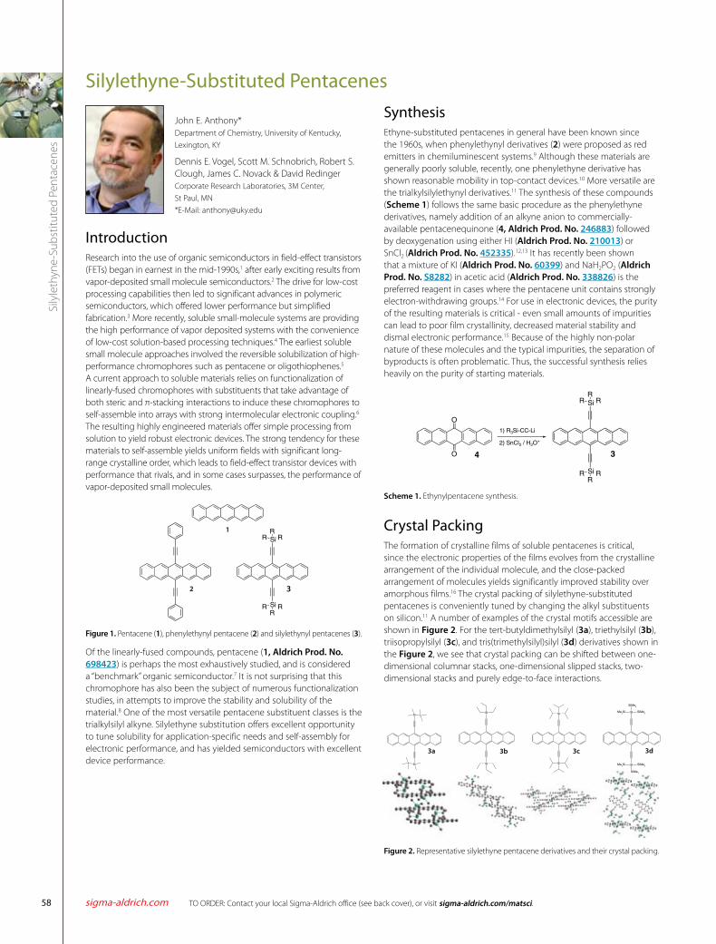
Crystal PackingThe formation of crystalline films of soluble pentacenes is critical, since the electronic properties of the films evolves from the crystalline arrangement of the individual molecule, and the close-packed arrangement of molecules yields significantly improved stability over amorphous films.16 The crystal packing of silylethyne-substituted pentacenes is conveniently tuned by changing the alkyl substituents on silicon.11 A number of examples of the crystal motifs accessible are shown in Figure 2. For the tert-butyldimethylsilyl (3a), triethylsilyl (3b), triisopropylsilyl (3c), and tris(trimethylsilyl)silyl (3d) derivatives shown in the Figure 2, we see that crystal packing can be shifted between one-dimensional columnar stacks, one-dimensional slipped stacks, two-dimensional stacks and purely edge-to-face interactions.
Si
Si
3a
Si
Si
3b
Si
Si
3c
Si
SiMe3
Me3Si SiMe3
Si SiMe3
SiMe3
3d
Me3Si
Figure 2. Representative silylethyne pentacene derivatives and their crystal packing.
Silylethyne-Substituted Pentacenes
For questions, product data, or new product suggestions, please contact Aldrich Materials Science at [email protected]. 59
Silylethyne-Substituted Pentacenes
Intrinsic PropertiesFor planar devices (such as FETs), we have found that materials with two-dimensional π-stacking interactions yield the most uniform films and provide the best device performance. Of these, the 6,13-bis(triisopropylsilylethynyl) pentacene derivative (TIPS pentacene 3c (Aldrich Prod. No. 716006)) has proven to be quite successful for applications in organic electronics and is the most intensively studied soluble pentacene. Band structure calculations on a variety of silylethyne-substituted pentacenes show significant dispersion in both the conduction and valence bands, predicting significant potential for high hole and electron mobility.17 This potential was confirmed by optical pump-THz probe studies on single crystals of TIPS pentacene 3c and triethylsilyl derivative 3b, showing that both materials exhibit mobilities of the same order as that of unsubstituted pentacene.18
OFETsDevice applications of this class of compounds were first reported in 2003, with the analysis of vapor-deposited films of a series of silylethyne-functionalized pentacenes in bottom-contact transistors.19 A key finding of these studies was the need to heat the device substrates to over 85°C during deposition in order to achieve suitably crystalline films. Contrary to the all-optical studies performed on single crystals, the thin-film studies showed dramatic differences in performance between 1-D and 2-D π-stacked materials, with the 2-D materials (3c, μFET = 0.4 cm2/Vs) vastly outperforming a variety of 1-D stacked compounds (e.g. 3b, μFET = 10-5 cm2/Vs). These differences likely arise from differences in film morphology; TIPS compound 3c grew on the substrate as wide needles or plates, while TES derivative 3b grew as thin needles with poor substrate coverage.20 Subsequent studies of solution-deposited films, where the slow solvent evaporation rate allows the pentacene to self-organize during crystallization, showed significantly improved performance in FET devices based on TIPS pentacene, with hole mobility as high as 1.8 cm2/Vs observed in films cast from toluene.21 Careful selection of casting solvent is critical to yield high quality films and stable device performance.22
SemiconductorDrainSource
SiO2 dielectric layer
Doped Si gate electrode
Figure 3. Bottom-contact field-effect transistor configuration, and a top-down picture of a bottom-contact device with semiconductor deposited.
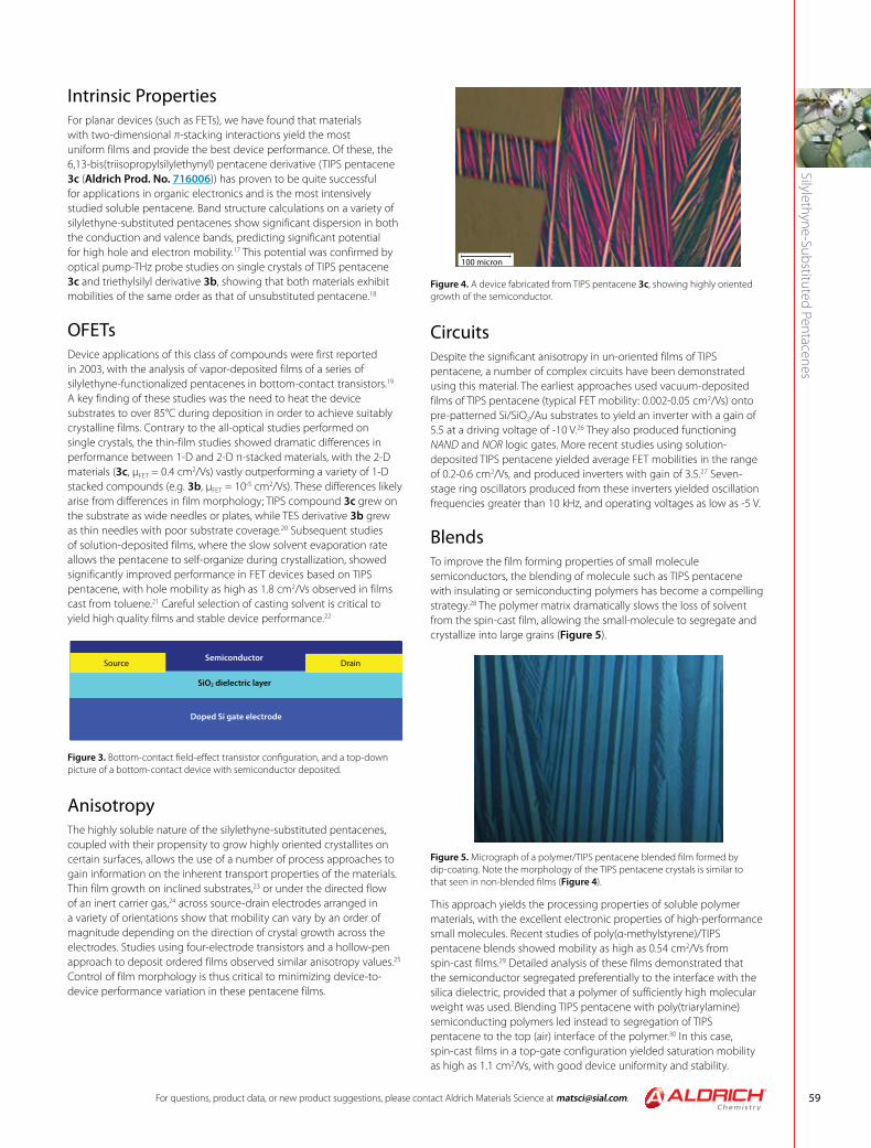
AnisotropyThe highly soluble nature of the silylethyne-substituted pentacenes, coupled with their propensity to grow highly oriented crystallites on certain surfaces, allows the use of a number of process approaches to gain information on the inherent transport properties of the materials. Thin film growth on inclined substrates,23 or under the directed flow of an inert carrier gas,24 across source-drain electrodes arranged in a variety of orientations show that mobility can vary by an order of magnitude depending on the direction of crystal growth across the electrodes. Studies using four-electrode transistors and a hollow-pen approach to deposit ordered films observed similar anisotropy values.25 Control of film morphology is thus critical to minimizing device-to-device performance variation in these pentacene films.
100 micron
Figure 4. A device fabricated from TIPS pentacene 3c, showing highly oriented growth of the semiconductor.
CircuitsDespite the significant anisotropy in un-oriented films of TIPS pentacene, a number of complex circuits have been demonstrated using this material. The earliest approaches used vacuum-deposited films of TIPS pentacene (typical FET mobility: 0.002-0.05 cm2/Vs) onto pre-patterned Si/SiO2/Au substrates to yield an inverter with a gain of 5.5 at a driving voltage of -10 V.26 They also produced functioning NAND and NOR logic gates. More recent studies using solution-deposited TIPS pentacene yielded average FET mobilities in the range of 0.2-0.6 cm2/Vs, and produced inverters with gain of 3.5.27 Seven-stage ring oscillators produced from these inverters yielded oscillation frequencies greater than 10 kHz, and operating voltages as low as -5 V.
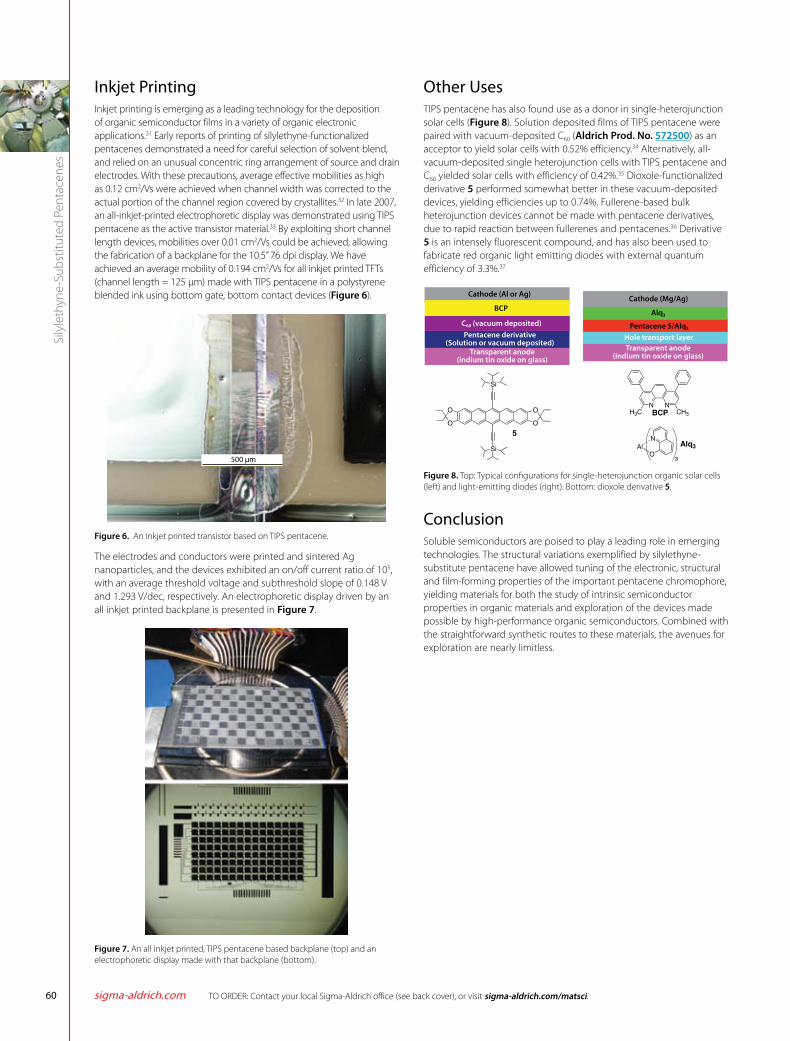
BlendsTo improve the film forming properties of small molecule semiconductors, the blending of molecule such as TIPS pentacene with insulating or semiconducting polymers has become a compelling strategy.28 The polymer matrix dramatically slows the loss of solvent from the spin-cast film, allowing the small-molecule to segregate and crystallize into large grains (Figure 5).
Figure 5. Micrograph of a polymer/TIPS pentacene blended film formed by dip-coating. Note the morphology of the TIPS pentacene crystals is similar to that seen in non-blended films (Figure 4).
This approach yields the processing properties of soluble polymer materials, with the excellent electronic properties of high-performance small molecules. Recent studies of poly(α-methylstyrene)/TIPS pentacene blends showed mobility as high as 0.54 cm2/Vs from spin-cast films.29 Detailed analysis of these films demonstrated that the semiconductor segregated preferentially to the interface with the silica dielectric, provided that a polymer of sufficiently high molecular weight was used. Blending TIPS pentacene with poly(triarylamine) semiconducting polymers led instead to segregation of TIPS pentacene to the top (air) interface of the polymer.30 In this case, spin-cast films in a top-gate configuration yielded saturation mobility as high as 1.1 cm2/Vs, with good device uniformity and stability.
TO ORDER: Contact your local Sigma-Aldrich office (see back cover), or visit sigma-aldrich.com/matsci.sigma-aldrich.com60
Sily
leth
yne-
Subs
titut
ed P
enta
cene
s
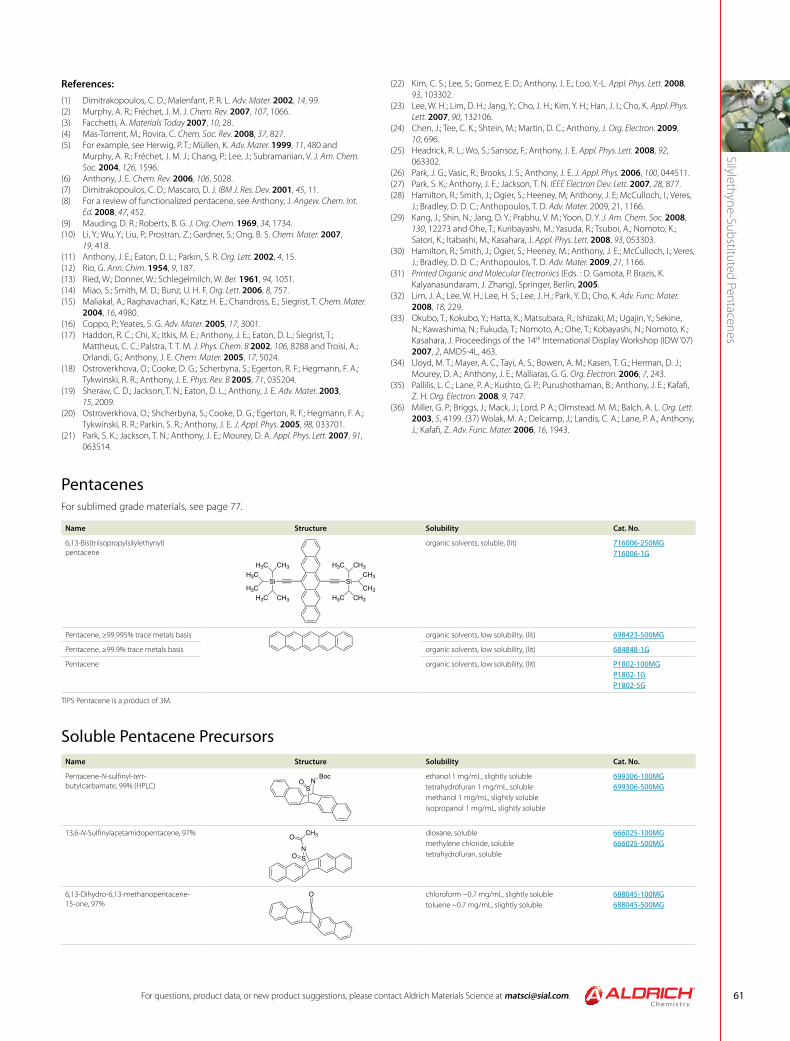
Inkjet PrintingInkjet printing is emerging as a leading technology for the deposition of organic semiconductor films in a variety of organic electronic applications.31 Early reports of printing of silylethyne-functionalized pentacenes demonstrated a need for careful selection of solvent blend, and relied on an unusual concentric ring arrangement of source and drain electrodes. With these precautions, average effective mobilities as high as 0.12 cm2/Vs were achieved when channel width was corrected to the actual portion of the channel region covered by crystallites.32 In late 2007, an all-inkjet-printed electrophoretic display was demonstrated using TIPS pentacene as the active transistor material.33 By exploiting short channel length devices, mobilities over 0.01 cm2/Vs could be achieved, allowing the fabrication of a backplane for the 10.5” 76 dpi display. We have achieved an average mobility of 0.194 cm2/Vs for all inkjet printed TFTs (channel length = 125 μm) made with TIPS pentacene in a polystyrene blended ink using bottom gate, bottom contact devices (Figure 6).
500 μm
Figure 6. An inkjet printed transistor based on TIPS pentacene.
The electrodes and conductors were printed and sintered Ag nanoparticles, and the devices exhibited an on/off current ratio of 105, with an average threshold voltage and subthreshold slope of 0.148 V and 1.293 V/dec, respectively. An electrophoretic display driven by an all inkjet printed backplane is presented in Figure 7.
Figure 7. An all inkjet printed, TIPS pentacene based backplane (top) and an electrophoretic display made with that backplane (bottom).
Other UsesTIPS pentacene has also found use as a donor in single-heterojunction solar cells (Figure 8). Solution deposited films of TIPS pentacene were paired with vacuum-deposited C60 (Aldrich Prod. No. 572500) as an acceptor to yield solar cells with 0.52% efficiency.34 Alternatively, all-vacuum-deposited single heterojunction cells with TIPS pentacene and C60 yielded solar cells with efficiency of 0.42%.35 Dioxole-functionalized derivative 5 performed somewhat better in these vacuum-deposited devices, yielding efficiencies up to 0.74%. Fullerene-based bulk heterojunction devices cannot be made with pentacene derivatives, due to rapid reaction between fullerenes and pentacenes.36 Derivative 5 is an intensely fluorescent compound, and has also been used to fabricate red organic light emitting diodes with external quantum efficiency of 3.3%.37
Cathode (Al or Ag)
BCP
C60 (vacuum deposited)Pentacene derivative
(Solution or vacuum deposited)Transparent anode
(indium tin oxide on glass)
Cathode (Mg/Ag)
Alq3
Pentacene 5/Alq3
Hole transport layerTransparent anode
(indium tin oxide on glass)
Si
Si
5
O
O O
ON N
CH3H3C BCP
N
OAl
3
Alq3
Figure 8. Top: Typical configurations for single-heterojunction organic solar cells (left) and light-emitting diodes (right). Bottom: dioxole derivative 5.
ConclusionSoluble semiconductors are poised to play a leading role in emerging technologies. The structural variations exemplified by silylethyne-substitute pentacene have allowed tuning of the electronic, structural and film-forming properties of the important pentacene chromophore, yielding materials for both the study of intrinsic semiconductor properties in organic materials and exploration of the devices made possible by high-performance organic semiconductors. Combined with the straightforward synthetic routes to these materials, the avenues for exploration are nearly limitless.
For questions, product data, or new product suggestions, please contact Aldrich Materials Science at [email protected]. 61
Silylethyne-Substituted Pentacenes
References:(1) Dimitrakopoulos, C. D.; Malenfant, P. R. L. Adv. Mater. 2002, 14, 99. (2) Murphy, A. R.; Fréchet, J. M. J. Chem. Rev. 2007, 107, 1066. (3) Facchetti, A. Materials Today 2007, 10, 28. (4) Mas-Torrent, M.; Rovira, C. Chem. Soc. Rev. 2008, 37, 827. (5) For example, see Herwig, P. T.; Müllen, K. Adv. Mater. 1999, 11, 480 and
Murphy, A. R.; Fréchet, J. M. J.; Chang, P.; Lee, J.; Subramanian, V. J. Am. Chem. Soc. 2004, 126, 1596.
(6) Anthony, J. E. Chem. Rev. 2006, 106, 5028. (7) Dimitrakopoulos, C. D.; Mascaro, D. J. IBM J. Res. Dev. 2001, 45, 11.(8) For a review of functionalized pentacene, see Anthony, J. Angew. Chem. Int.
Ed. 2008, 47, 452.(9) Mauding, D. R.; Roberts, B. G. J. Org. Chem. 1969, 34, 1734. (10) Li, Y.; Wu, Y.; Liu, P.; Prostran, Z.; Gardner, S.; Ong, B. S. Chem. Mater. 2007,
19, 418.(11) Anthony, J. E.; Eaton, D. L.; Parkin, S. R. Org. Lett. 2002, 4, 15. (12) Rio, G. Ann. Chim. 1954, 9, 187.(13) Ried, W.; Donner, W.; Schlegelmilch, W. Ber. 1961, 94, 1051.(14) Miao, S.; Smith, M. D.; Bunz, U. H. F. Org. Lett. 2006, 8, 757.(15) Maliakal, A.; Raghavachari, K.; Katz, H. E.; Chandross, E.; Siegrist, T. Chem. Mater.
2004, 16, 4980.(16) Coppo, P.; Yeates, S. G. Adv. Mater. 2005, 17, 3001.(17) Haddon, R. C.; Chi, X.; Itkis, M. E.; Anthony, J. E.; Eaton, D. L.; Siegrist, T.;
Mattheus, C. C.; Palstra, T. T. M. J. Phys. Chem. B 2002, 106, 8288 and Troisi, A.; Orlandi, G.; Anthony, J. E. Chem. Mater. 2005, 17, 5024.
(18) Ostroverkhova, O.; Cooke, D. G.; Scherbyna, S.; Egerton, R. F.; Hegmann, F. A.; Tykwinski, R. R.; Anthony, J. E. Phys. Rev. B 2005, 71, 035204.
(19) Sheraw, C. D.; Jackson, T. N.; Eaton, D. L.; Anthony, J. E. Adv. Mater. 2003, 15, 2009.
(20) Ostroverkhova, O.; Shcherbyna, S.; Cooke, D. G.; Egerton, R. F.; Hegmann, F. A.; Tykwinski, R. R.; Parkin, S. R.; Anthony, J. E. J. Appl. Phys. 2005, 98, 033701.
(21) Park, S. K.; Jackson, T. N.; Anthony, J. E.; Mourey, D. A. Appl. Phys. Lett. 2007, 91, 063514.
(22) Kim, C. S.; Lee, S.; Gomez, E. D.; Anthony, J. E.; Loo, Y.-L. Appl. Phys. Lett. 2008, 93, 103302.
(23) Lee, W. H.; Lim, D. H.; Jang, Y.; Cho, J. H.; Kim, Y. H.; Han, J. I.; Cho, K. Appl. Phys. Lett. 2007, 90, 132106.
(24) Chen, J.; Tee, C. K.; Shtein, M.; Martin, D. C.; Anthony, J. Org. Electron. 2009, 10, 696.
(25) Headrick, R. L.; Wo, S.; Sansoz, F.; Anthony, J. E. Appl. Phys. Lett. 2008, 92, 063302.
(26) Park, J. G.; Vasic, R.; Brooks, J. S.; Anthony, J. E. J. Appl. Phys. 2006, 100, 044511. (27) Park, S. K.; Anthony, J. E.; Jackson, T. N. IEEE Electron Dev. Lett. 2007, 28, 877. (28) Hamilton, R.; Smith, J.; Ogier, S.; Heeney, M; Anthony, J. E; McCulloch, I.; Veres,
J.; Bradley, D. D. C.; Anthopoulos, T. D. Adv. Mater. 2009, 21, 1166.(29) Kang, J.; Shin, N.; Jang, D. Y.; Prabhu, V. M.; Yoon, D. Y. J. Am. Chem. Soc. 2008,
130, 12273 and Ohe, T.; Kuribayashi, M.; Yasuda, R.; Tsuboi, A.; Nomoto, K.; Satori, K.; Itabashi, M.; Kasahara, J. Appl. Phys. Lett. 2008, 93, 053303.
(30) Hamilton, R.; Smith, J.; Ogier, S.; Heeney, M.; Anthony, J. E.; McCulloch, I.; Veres, J.; Bradley, D. D. C.; Anthopoulos, T. D. Adv. Mater. 2009, 21, 1166.
(31) Printed Organic and Molecular Electronics (Eds. : D. Gamota, P. Brazis, K. Kalyanasundaram, J. Zhang), Springer, Berlin, 2005.
(32) Lim, J. A.; Lee, W. H.; Lee, H. S.; Lee, J. H.; Park, Y. D.; Cho, K. Adv. Func. Mater. 2008, 18, 229.
(33) Okubo, T.; Kokubo, Y.; Hatta, K.; Matsubara, R.; Ishizaki, M.; Ugajin, Y.; Sekine, N.; Kawashima, N.; Fukuda, T.; Nomoto, A.; Ohe, T.; Kobayashi, N.; Nomoto, K.; Kasahara, J. Proceedings of the 14th International Display Workshop (IDW ‘07) 2007, 2, AMD5-4L, 463.
(34) Lloyd, M. T.; Mayer, A. C.; Tayi, A. S.; Bowen, A. M.; Kasen, T. G.; Herman, D. J.; Mourey, D. A.; Anthony, J. E.; Malliaras, G. G. Org. Electron. 2006, 7, 243.
(35) Pallilis, L. C.; Lane, P. A.; Kushto, G. P.; Purushothaman, B.; Anthony, J. E.; Kafafi, Z. H. Org. Electron. 2008, 9, 747.
(36) Miller, G. P.; Briggs, J.; Mack, J.; Lord, P. A.; Olmstead, M. M.; Balch, A. L. Org. Lett. 2003, 5, 4199. (37) Wolak, M. A.; Delcamp, J.; Landis, C. A.; Lane, P. A.; Anthony, J.; Kafafi, Z. Adv. Func. Mater. 2006, 16, 1943.
PentacenesFor sublimed grade materials, see page 77.
Name Structure Solubility Cat. No.
6,13-Bis(triisopropylsilylethynyl)pentacene
SiSi
CH3H3C
CH3CH3
CH3
H3C
H3C
H3CH3C
H3C CH3
CH3
organic solvents, soluble, (lit) 716006-250MG716006-1G
Pentacene, ≥99.995% trace metals basis organic solvents, low solubility, (lit) 698423-500MG
Pentacene, ≥99.9% trace metals basis organic solvents, low solubility, (lit) 684848-1G
Pentacene organic solvents, low solubility, (lit) P1802-100MGP1802-1GP1802-5G
TIPS Pentacene is a product of 3M.
Soluble Pentacene PrecursorsName Structure Solubility Cat. No.
Pentacene-N-sulfinyl-tert-butylcarbamate, 99% (HPLC) S
NOBoc ethanol 1 mg/mL, slightly soluble
tetrahydrofuran 1 mg/mL, solublemethanol 1 mg/mL, slightly solubleisopropanol 1 mg/mL, slightly soluble
699306-100MG699306-500MG
13,6-N-Sulfinylacetamidopentacene, 97%
SN
O
OCH3 dioxane, soluble
methylene chloride, solubletetrahydrofuran, soluble
666025-100MG666025-500MG
6,13-Dihydro-6,13-methanopentacene-15-one, 97%
O chloroform ~0.7 mg/mL, slightly solubletoluene ~0.7 mg/mL, slightly soluble
688045-100MG688045-500MG
TO ORDER: Contact your local Sigma-Aldrich office (see back cover), or visit sigma-aldrich.com/matsci.sigma-aldrich.com62
Sily
leth
yne-
Subs
titut
ed P
enta
cene
s
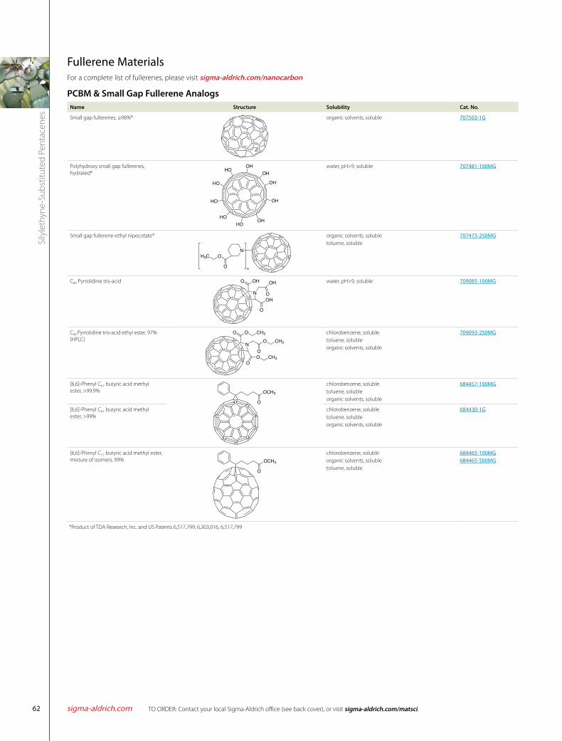
Fullerene MaterialsFor a complete list of fullerenes, please visit sigma-aldrich.com/nanocarbon
PCBM & Small Gap Fullerene AnalogsName Structure Solubility Cat. No.
Small gap fullerenes, ≥98%* organic solvents, soluble 707503-1G
Polyhydroxy small gap fullerenes, hydrated*
OH
OH
OHHO
HO
HO
HO
HOOH
OH
water, pH>9, soluble 707481-100MG
Small gap fullerene-ethyl nipecotate*
NOH3C
O x
organic solvents, solubletoluene, soluble
707473-250MG
C60 Pyrrolidine tris-acid
N
OHO
O
OH
OH
O
water, pH>9, soluble 709085-100MG
C60 Pyrrolidine tris-acid ethyl ester, 97% (HPLC)
N
OO
O CH3
O
CH3
O CH3O
chlorobenzene, solubletoluene, solubleorganic solvents, soluble
709093-250MG
[6,6]-Phenyl C61 butyric acid methyl ester, >99.9% OCH3
O
chlorobenzene, solubletoluene, solubleorganic solvents, soluble
684457-100MG
[6,6]-Phenyl C61 butyric acid methyl ester, >99%
chlorobenzene, solubletoluene, solubleorganic solvents, soluble
684430-1G
[6,6]-Phenyl C71 butyric acid methyl ester, mixture of isomers, 99%
O
OCH3
chlorobenzene, solubleorganic solvents, solubletoluene, soluble
684465-100MG684465-500MG
*Product of TDA Research, Inc. and US Patents 6,517,799, 6,303,016, 6,517,799
For questions, product data, or new product suggestions, please contact Aldrich Materials Science at [email protected]. 63
Silylethyne-Substituted Pentacenes
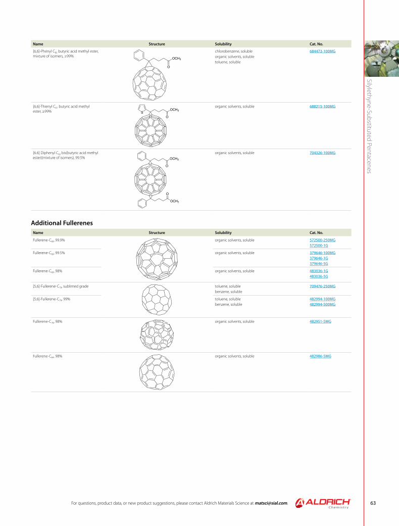
Name Structure Solubility Cat. No.
[6,6]-Phenyl C85 butyric acid methyl ester, mixture of isomers, ≥99%
OCH3
O
chlorobenzene, solubleorganic solvents, solubletoluene, soluble
684473-100MG
[6,6]-Thienyl C61 butyric acid methyl ester, ≥99% OCH3
OS
organic solvents, soluble 688215-100MG
[6.6] Diphenyl C62 bis(butyric acid methyl ester)(mixture of isomers), 99.5% OCH3
O
OCH3
O
organic solvents, soluble 704326-100MG
Additional FullerenesName Structure Solubility Cat. No.
Fullerene-C60, 99.9% organic solvents, soluble 572500-250MG572500-1G
Fullerene-C60, 99.5% organic solvents, soluble 379646-100MG379646-1G379646-5G
Fullerene-C60, 98% organic solvents, soluble 483036-1G483036-5G
[5,6]-Fullerene-C70, sublimed grade toluene, solublebenzene, soluble
709476-250MG
[5,6]-Fullerene-C70, 99% toluene, solublebenzene, soluble
482994-100MG482994-500MG
Fullerene-C76, 98% organic solvents, soluble 482951-5MG
Fullerene-C84, 98% organic solvents, soluble 482986-5MG
TO ORDER: Contact your local Sigma-Aldrich office (see back cover), or visit sigma-aldrich.com/matsci.sigma-aldrich.com64
Self-
Asse
mbl
ed N
anod
iele
ctric
s (SA
ND
s) fo
r Unc
onve
ntio
nal E
lect
roni
cs
Antonio Facchetti Polyera Corporation, www.polyera.com E-mail: [email protected]
Tobin J. Marks Department of Chemistry, Northwestern University, Evanston, IL E-mail: [email protected]
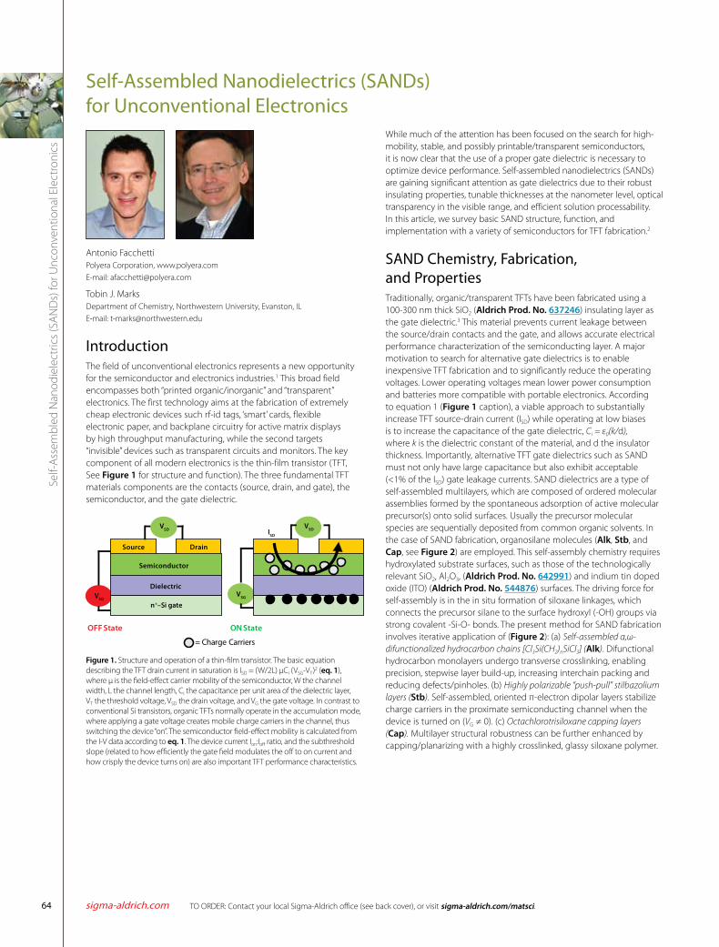
IntroductionThe field of unconventional electronics represents a new opportunity for the semiconductor and electronics industries.1 This broad field encompasses both “printed organic/inorganic” and “transparent” electronics. The first technology aims at the fabrication of extremely cheap electronic devices such rf-id tags, ‘smart’ cards, flexible electronic paper, and backplane circuitry for active matrix displays by high throughput manufacturing, while the second targets “invisible” devices such as transparent circuits and monitors. The key component of all modern electronics is the thin-film transistor (TFT, See Figure 1 for structure and function). The three fundamental TFT materials components are the contacts (source, drain, and gate), the semiconductor, and the gate dielectric.
Semiconductor
Source Drain
Dielectric
ISD
VSD
VSG
OFF State ON State
= Charge Carriers
VSG
VSD
n+–Si gate
Figure 1. Structure and operation of a thin-film transistor. The basic equation describing the TFT drain current in saturation is ISD = (W/2L) μCi (VSG-VT)2 (eq. 1), where μ is the field-effect carrier mobility of the semiconductor, W the channel width, L the channel length, Ci the capacitance per unit area of the dielectric layer, VT the threshold voltage, VSD the drain voltage, and VG the gate voltage. In contrast to conventional Si transistors, organic TFTs normally operate in the accumulation mode, where applying a gate voltage creates mobile charge carriers in the channel, thus switching the device “on”. The semiconductor field-effect mobility is calculated from the I-V data according to eq. 1. The device current Ion:Ioff ratio, and the subthreshold slope (related to how efficiently the gate field modulates the off to on current and how crisply the device turns on) are also important TFT performance characteristics.
While much of the attention has been focused on the search for high-mobility, stable, and possibly printable/transparent semiconductors, it is now clear that the use of a proper gate dielectric is necessary to optimize device performance. Self-assembled nanodielectrics (SANDs) are gaining significant attention as gate dielectrics due to their robust insulating properties, tunable thicknesses at the nanometer level, optical transparency in the visible range, and efficient solution processability. In this article, we survey basic SAND structure, function, and implementation with a variety of semiconductors for TFT fabrication.2
SAND Chemistry, Fabrication, and PropertiesTraditionally, organic/transparent TFTs have been fabricated using a 100-300 nm thick SiO2 (Aldrich Prod. No. 637246) insulating layer as the gate dielectric.3 This material prevents current leakage between the source/drain contacts and the gate, and allows accurate electrical performance characterization of the semiconducting layer. A major motivation to search for alternative gate dielectrics is to enable inexpensive TFT fabrication and to significantly reduce the operating voltages. Lower operating voltages mean lower power consumption and batteries more compatible with portable electronics. According to equation 1 (Figure 1 caption), a viable approach to substantially increase TFT source-drain current (ISD) while operating at low biases is to increase the capacitance of the gate dielectric, Ci = ε0(k/d), where k is the dielectric constant of the material, and d the insulator thickness. Importantly, alternative TFT gate dielectrics such as SAND must not only have large capacitance but also exhibit acceptable (<1% of the ISD) gate leakage currents. SAND dielectrics are a type of self-assembled multilayers, which are composed of ordered molecular assemblies formed by the spontaneous adsorption of active molecular precursor(s) onto solid surfaces. Usually the precursor molecular species are sequentially deposited from common organic solvents. In the case of SAND fabrication, organosilane molecules (Alk, Stb, and Cap, see Figure 2) are employed. This self-assembly chemistry requires hydroxylated substrate surfaces, such as those of the technologically relevant SiO2, Al2O3, (Aldrich Prod. No. 642991) and indium tin doped oxide (ITO) (Aldrich Prod. No. 544876) surfaces. The driving force for self-assembly is in the in situ formation of siloxane linkages, which connects the precursor silane to the surface hydroxyl (-OH) groups via strong covalent -Si-O- bonds. The present method for SAND fabrication involves iterative application of (Figure 2): (a) Self-assembled α,ω-difunctionalized hydrocarbon chains [Cl3Si(CH2)nSiCl3] (Alk). Difunctional hydrocarbon monolayers undergo transverse crosslinking, enabling precision, stepwise layer build-up, increasing interchain packing and reducing defects/pinholes. (b) Highly polarizable “push-pull” stilbazolium layers (Stb). Self-assembled, oriented π-electron dipolar layers stabilize charge carriers in the proximate semiconducting channel when the device is turned on (VG ≠ 0). (c) Octachlorotrisiloxane capping layers (Cap). Multilayer structural robustness can be further enhanced by capping/planarizing with a highly crosslinked, glassy siloxane polymer.
Self-Assembled Nanodielectrics (SANDs) for Unconventional Electronics
For questions, product data, or new product suggestions, please contact Aldrich Materials Science at [email protected]. 65
Self-Assembled N
anodielectrics (SAND
s) for Unconventional Electronics
N
NN
N
O O
Cl2ISi
I
TBOMS TBOMS
HO
HO
HO
HO
SemiconductorS D
v. Semiconductorsvi. Au, Al
i. Alk
iii. Stb
ii. CapOSi
OOSi
OSiSi
OSiO
OSi
OSiSi O O O O
N
NN
N
O O
N
NN
N
O O
N
NN
N
O OOSi
OOSi
OSiSi
OSiO
OSiO
SiSi
O
O O O OO
I I I
3
3OSiOSiOSiOHSi
SiO O Si
O O SiO O Si
O O
( )( )( )( )7 7 7 7
O O O OSi
Si
Cl Cl
Cl Cl Cl
Cl
( ) 7Other Semiconductors
SAND
Organic Semiconductors
N
N N
N N
N
N
N
FF
FF
FF
FF
F
FF
F
FF
FF
Cu
SS
SS
O
C6F13
O
C6F13
NN
O
O
O
O
C8H17C8H17
SS
SS
SS
SS
SS
SS
C6H13
C6H13
CN
NC
ClSi
OSi
OSi
Cl
Cl Cl
Cl Cl
ClCl
iv. Cap
PentaceneActivlnk P0300
6T
Activlnk N0800
Activlnk N1200 CuFPc
•Nanowire: In2O3, SnO, ZnO
•Nanotubes: SWCNT•Thin Film: In2O3, In2-xSnxO3, CdSe
n+–Si, Al, ITOn+–Si, Al, ITO
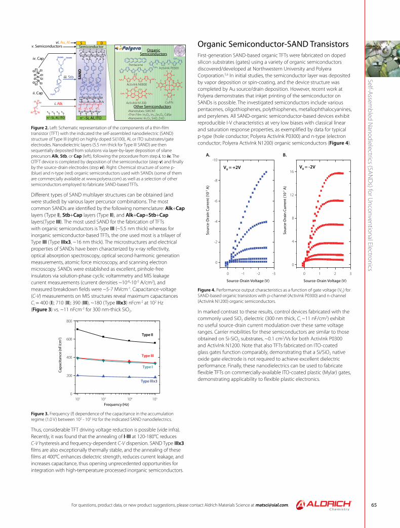
Figure 2. Left: Schematic representation of the components of a thin-film transistor (TFT) with the indicated the self-assembled nanodielectric (SAND) structure of Type III (right) on highly doped Si(100), Al, or ITO substrates/gate electrodes. Nanodielectric layers (5.5 nm thick for Type III SAND) are then sequentially deposited from solutions via layer-by-layer deposition of silane precursors Alk, Stb, or Cap (left), following the procedure from step i. to iv. The OTFT device is completed by deposition of the semiconductor (step v) and finally by the source-drain electrodes (step vi). Right: Chemical structure of some p- (blue) and n-type (red) organic semiconductors used with SANDs (some of them are commercially available at www.polyera.com) as well as a selection of other semiconductors employed to fabricate SAND-based TFTs.
Different types of SAND multilayer structures can be obtained (and were studied) by various layer percursor combinations. The most common SANDs are identified by the following nomenclature: Alk+Cap layers (Type I), Stb+Cap layers (Type II), and Alk+Cap+Stb+Cap layers(Type III). The most used SAND for the fabrication of TFTs with organic semiconductors is Type III (~5.5 nm thick) whereas for inorganic semiconductor-based TFTs, the one used most is a trilayer of Type III (Type IIIx3, ~16 nm thick). The microstructures and electrical properties of SANDs have been characterized by x-ray reflectivity, optical absorption spectroscopy, optical second-harmonic generation measurements, atomic force microscopy, and scanning electron microscopy. SANDs were established as excellent, pinhole-free insulators via solution-phase cyclic voltammetry and MIS leakage current measurements (current densities ~10-8-10-5 A/cm2), and measured breakdown fields were ~5-7 MVcm-1. Capacitance-voltage (C-V) measurements on MIS structures reveal maximum capacitances Ci = 400 (I); 710 (II); 390 (III), ~180 (Type IIIx3) nFcm-2 at 102 Hz (Figure 3) vs. ~11 nFcm-2 for 300 nm-thick SiO2.
102 103 104 105
0
200
400
600
800
Capa
cita
nce
(nF/
cm2 )
Frequency (Hz)
Type I
Type II
Type III
Type IIIx3
Figure 3. Frequency (f) dependence of the capacitance in the accumulation regime (1.0 V) between 102 - 105 Hz for the indicated SAND nanodielectrics.
Thus, considerable TFT driving voltage reduction is possible (vide infra). Recently, it was found that the annealing of I-III at 120-180°C reduces C-V hysteresis and frequency-dependent C-V dispersion. SAND Type IIIx3 films are also exceptionally thermally stable, and the annealing of these films at 400°C enhances dielectric strength, reduces current leakage, and increases capacitance, thus opening unprecedented opportunities for integration with high-temperature processed inorganic semiconductors.
Organic Semiconductor-SAND TransistorsFirst-generation SAND-based organic TFTs were fabricated on doped silicon substrates (gates) using a variety of organic semiconductors discovered/developed at Northwestern University and Polyera Corporation.5,6 In initial studies, the semiconductor layer was deposited by vapor deposition or spin-coating, and the device structure was completed by Au source/drain deposition. However, recent work at Polyera demonstrates that inkjet printing of the semiconductor on SANDs is possible. The investigated semiconductors include various pentacenes, oligothiophenes, polythiophenes, metallophthalocyanines, and perylenes. All SAND-organic semiconductor-based devices exhibit reproducible I-V characteristics at very low biases with classical linear and saturation response properties, as exemplified by data for typical p-type (hole conductor; Polyera ActivInk P0300) and n-type (electron conductor; Polyera ActivInk N1200) organic semiconductors (Figure 4).
0 1 2 3
0
4
8
12
16
Source-Drain Voltage (V)
0 -1 -2 -3
0
-2
-4
-6
-8
-10
Source-Drain Voltage (V)
Sour
ce-D
rain
Cur
rent
(10-7
A)
Sour
ce-D
rain
Cur
rent
(10-7
A)
A. B.
Vg = +2V Vg = -2V
Figure 4. Performance output characteristics as a function of gate voltage (VG) for SAND-based organic transistors with p-channel (ActivInk P0300) and n-channel (ActivInk N1200) organic semiconductors.
In marked contrast to these results, control devices fabricated with the commonly used SiO2 dielectric (300 nm thick, Ci ~11 nF/cm2) exhibit no useful source-drain current modulation over these same voltage ranges. Carrier mobilities for these semiconductors are similar to those obtained on Si-SiO2 substrates, ~0.1 cm2/Vs for both ActivInk P0300 and ActivInk N1200. Note that also TFTs fabricated on ITO-coated glass gates function comparably, demonstrating that a Si/SiO2 native oxide gate electrode is not required to achieve excellent dielectric performance. Finally, these nanodielectrics can be used to fabricate flexible TFTs on commercially-available ITO-coated plastic (Mylar) gates, demonstrating applicability to flexible plastic electronics.
TO ORDER: Contact your local Sigma-Aldrich office (see back cover), or visit sigma-aldrich.com/matsci.sigma-aldrich.com66
Self-
Asse
mbl
ed N
anod
iele
ctric
s (SA
ND
s) fo
r Unc
onve
ntio
nal E
lect
roni
cs
Inorganic Semiconductor-SAND Transistors and CircuitsWe next investigated SAND compatibility with semiconductors other than small organic molecules. We first demonstrated the compatibility of Type IIIx3 SAND with single-wall carbon nanotubes (SWCNTs) (Aldrich Prod. No. 704113, 704121, 704148) as the semiconductor.7 SWCNTs where grown by CVD onto SiO2/Si wafers and transfer printed (~10 tubes/μm2) directly onto the Si-SAND substrates (and control Si/SiO2 substrates). Good SWNT-SAND adhesion allows direct photolithographic patterning of the source and drain electrodes by liftoff. It is found that TFT performance is significantly improved over control devices using 100 nm Si/SiO2 gate dielectrics, with substantially lowered hysteresis and VT shifts. Thus, the TFT mobility is excellent with μhole ~5.6 cm2/Vs, VT = 0.2 V, and a low gate leakage current of ~10 nA at VG = -1 V demonstrated. Furthermore, compatibility with n-type SWCNTs (those having a PEI coating) is demonstrated, with small observed hysteresis and TFT properties: μelectron = 4.1 cm2/Vs and VT = -2 V. Compatibility of SAND dielectrics with thin-film inorganic semiconductors was demonstrated by using In2O3 thin-films (Aldrich Prod. No. 203424) to enable high-performance, low-voltage, and fully transparent TFTs.8 In2O3 is a wide-bandgap (3.6-3.75 eV) n-type semiconductor with excellent transparency in the visible region (>90%). Thin films of In2O3 were deposited at room temperature by ion-assisted deposition (IAD) directly on top of the SAND dielectric, and device fabrication completed by Au source/drain contact deposition. Note that the SAND is stable to the in-situ ion/plasma exposure during In2O3 deposition. Significant In2O3 TFT performance enhancement is observed with SAND-gated devices, where μ = 140 cm2/Vs, interfacial trap density, D = 1011 cm-2, VT = 0.0 V (with nearly hysteretic free response), on/off = 105, and the subthreshold slope = 150 mV/decade. These metrics can be compared to the performance on Si/SiO2-gated devices where μ = 10 cm2/Vs and on/off = 105. To realize fully transparent TFTs, the same fabrication procedures were followed except utilizing glass/ITO as the bottom gate electrode and doped In2O3 source and drain electrodes. The performance of SAND-based transparent TFTs is essentially the same as on n+-Si substrates but with an improved subthreshold slope = 90 mV/decade.
The versatility of SAND as an effective gate dielectric for non-organic semiconductors was further demonstrated in TFTs using ZnO, In2O3, and SnO nanowires (NWs).9 As an example, ZnO NW (nanowire) TFTs with SAND IIIx3 as the gate dielectric were fabricated with ZnO nanowires (80 nm average diameter, and 5 μm average length) dispersed in 2-propanol (Aldrich Prod. No. 278475) and then transferred to the SAND-coated Si substrates. Source and drain Al electrodes were deposited by electron beam evaporation and patterned by photolithography. The SAND dielectrics were first electrically characterized in MIS devices (Al/SAND/Si), where a leakage current density of ~10-8 A/cm2 was measured, verifying SAND compatibility with the photolithographic and e-beam evaporation methodologies. SAND gated ZnO2 NW-TFTs reduced operating voltages to <1.5 V (from >1.5 V on Si/SiO2), while maintaining the device on/off ratio, increasing the on-current to 2 μA (from 0.3 μA), and increasing the mobility and transconductance. The VT of SAND gated ZnO NW-TFTs is -0.4 V, and the subthreshold slope is 400 mV/decade. High subthreshold slopes usually indicate surface traps, so the SAND-based ZnO NW-TFTs were then treated with ozone exposures, and indeed the subthreshold slope was reduced to 150 mV/decade. In addition, reduced VT values (0.2 V) and improved on:off ratios (108) were observed. The calculated electron mobility (taking into account the cylindrical geometry of the channel) is 196 cm2/Vs, which is far greater than 8-18 cm2/Vs measured for ZnO NW on thick Si/SiO2 dielectrics, and 54 cm2/Vs for a 70 nm thick SiO2 control dielectric. The TFT mobility varies from 164-181 cm2/Vs with variations in NW diameter and length. One of the remarkable properties of SAND-
based electronics is their resistance to radiation damage, known as radiation hardness. The proton (10 MeV H+) radiation tolerance was investigated first for SAND IIIx3/ZnO-NW TFTs.10 After various dosing and exposure conditions in a nuclear reactor, neither the leakage current nor the VT of the SAND-gated TFTs shifts significantly. Currently SAND-gated organic and inorganic TFTs are on the International Space Station for additional radiation testing. These results suggested that the bulk oxide trap density and interface trap density formed in SAND (or at the SAND-ZnO NW interface) during H+ irradiation are significantly lower than in traditional SiO2 gate dielectrics. This prompted detailed studies of ZnO-NW TFTs using low-frequency noise and temperature-dependent I-V measurements to characterize the surface/interface states. Lower 1/f noise constants are found for SAND-based devices compared to SiO2-based devices, and it is concluded that the interface trap densities are comparable to those for the aforementioned SWCNT devices (D = ~1012 cm2V-1) by comparison of the Hooge’s constant metric. Larger temperature variations of the transfer curves, and larger threshold voltage shifts vs. temperature observed for SiO2/ZnO-NW TFTs versus the corresponding SAND-gated devices, provide further evidence that the SAND/ZnO-NW TFTs have exceptionally low interface trap and defect densities.
All of the processes described above demonstrate that SANDs are robust gate dielectrics compatible with a number of inorganic semiconductors. However, since the above semiconductor depositions were all carried out near room temperature, the question arises as to whether SAND is stable at higher temperatures. Very recently we demonstrated that SAND IIIx3 films are stable to 400°C, thus opening a broad range of processing possibilities at high temperatures.11 One particular challenge has been to implement organic dielectric materials with aqueous solution-processed inorganic semiconductors. To achieve this, we explored the compatibility of SAND-based TFTs with solution-processed cadmium selenide (CdSe) (Aldrich Prod. No. 244600), In2O3, and ITO as the semiconducting layers. As an example, the chemical bath deposition method was recently used to deposit the CdSe films on SAND IIIx3 gate dielectric layers. Optimum performance of on:off ratio = 106, VT = 3.0 V, and subthreshold slope = 0.26 V/decade was achieved for CdSe/SAND-based TFTs annealed at 400oC, which exhibit mobilities of ~40 cm2/Vs vs. ~4 cm2/Vs for the analogous SiO2-based devices. Excellent performance was also achieved with In2O3
12 and ITO as the TFT semiconductors.
500 1000 1500 2000 25000
20
40
60
80
100
Tran
smit
tanc
e (%
)
Wavelength (nm)
Glass/ITO/SANDGlass/ITO/SAND/In2O3
Glass/ITO/SAND/In2O3/In2O3
0.0 0.5 1.0 1.5 2.00.00.20.40.60.81.01.2
VDS (V)
I DS (x
10-3
A)
0.1 ~ 0.3 V0.4 V0.6 V
0.8 V
VG = 1.0 V
0 5 10 15 20 25 300.0
1.0
2.0
3.0
4.0
5.0
0 V20 V40 V
60 V
80 V
VG = 100 VI D
S (1
0-3 A
)
VDS (V)
A. B. C.
D.
ON
OFF
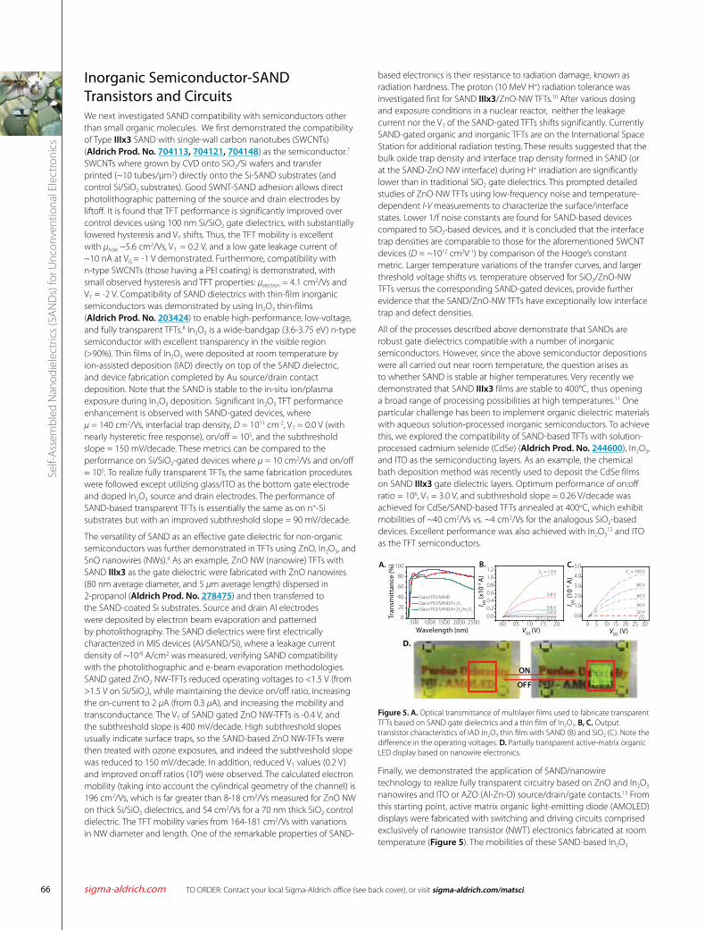
Figure 5. A. Optical transmittance of multilayer films used to fabricate transparent TFTs based on SAND gate dielectrics and a thin film of In2O3. B, C. Output transistor characteristics of IAD In2O3 thin film with SAND (B) and SiO2 (C). Note the difference in the operating voltages. D. Partially transparent active-matrix organic LED display based on nanowire electronics.
Finally, we demonstrated the application of SAND/nanowire technology to realize fully transparent circuitry based on ZnO and In2O3 nanowires and ITO or AZO (Al-Zn-O) source/drain/gate contacts.13 From this starting point, active matrix organic light-emitting diode (AMOLED) displays were fabricated with switching and driving circuits comprised exclusively of nanowire transistor (NWT) electronics fabricated at room temperature (Figure 5). The mobilities of these SAND-based In2O3
For questions, product data, or new product suggestions, please contact Aldrich Materials Science at [email protected]. 67
Self-Assembled N
anodielectrics (SAND
s) for Unconventional Electronics
NW TFTs are ~160 cm2/Vs, sufficient to drive bright display pixels. Fully transparent, proof-of-concept 2 x 2 mm NW-AMOLED arrays (300 pixels = 900 NWTs) were fabricated using very thin Al cathodes on glass substrates.12 The optical transmission values are ~72% (before OLED deposition) and ~35% (after OLED deposition; thinner Al is required) in the 350-1350 nm wavelength range, which corresponds to a green peak luminescence of >300 cd/m2. Note that transmission coefficients up to 70% have been reported for OLED structures on plastic substrates, although values in the 50% range are more common.
ConclusionsIn this short account, we briefly summarized the potential and promise of self-assembled multilayer gate dielectric films fabricated from silane precursors for organic, inorganic, and transparent TFTs, as well as for TFT circuitry and OLED displays. These materials beautifully illustrate the potential of molecular chemistry for constructing unusual and useful electronic materials.
AcknowledgmentsWe thank ONR (N00014-05-1-0766), AFOSR (FA9550-08-1-0331), and Polyera Corp. for support of this research, and the NSF-MRSEC program through the Northwestern University Materials Research Science and Engineering Center (DMR-0520513) for providing both support and characterization facilities. We thank all of our collaborators for the important and enthusiastic contributions to this work.
References:(1) (a) Sun, Y.; Rogers, J. A. Adv. Mater. 2007, 19, 1897. (b) Nomura, K.; Ohta, H.;
Takagi, A.; Kamiya, T.; Hirano, M.; Hosono, H. Nature 2004, 432 , 488. (c) Sun, B.; Peterson, R. L.; Sirringhaus, H.; Mori, K. J. Phys. Chem. C 2008, 111, 18831. (d) Murphy, A. R.; Frechet, J. M. J. Chem. Rev. 2007, 107, 1066. (e) Locklin, J.; Roberts, M.; Mannsfeld, S.; Bao, Z. Polym. Rev. 2006, 46, 79. (f ) Anthopoulos, T. D.; Setayesh, S.; Smits, E.; Colle, M.; Cantatore, E.; de Boer, B.; Blom, P. W. M.; de Leeuw, D. M. Adv. Mat. 2006, 18, 1900. (g) Chabinyc, M.; Loo, Y. L. J. Macromol. Sci. Polym. Rev. 2006, 46, 1. (h) Muccini, M Nature Mater. 2006, 5, 605. (i) Chua, L.-L.; Zaumseil, J.; Chang, J.-F.; Ou, E. C.-W.; Ho, P. K.-H.; Sirringhaus, H.; Friend, R. H. Nature 2005, 434, 194.
(2) DiBenedetto, S. A.; Facchetti, A.; Ratner, M. A.; Marks, T. J. Adv. Mater. 2009, 21, 1407.
(3) Facchetti, A.; Yoon, M.-H.; Marks, T. J. Adv. Mater, 2005, 17, 1705.(4) Yoon, M.-H.; Facchetti, A.; Marks, T.J. Proc. Nat. Acad. Sci. USA, 2005, 102, 4678.(5) Facchetti, A.; Deng, Y.; Wang, A.; Koide, Y.; Sirringhaus, H.; Marks, T. J.; Friend, R.
H. Angew. Chem., Int. Ed. 2000, 39, 4547.(6) Jones, B. A.; Ahrens, M. J.; Yoon, M.-H.; Facchetti, A.; Marks, T. J.; Wasielewski M.
R. Angew. Chem. Int. Ed. 2004, 43, 6363.(7) Hur, S.-H.; Yoon, M.-H.; Gaur, A.; Facchetti, A.; Marks, T. J.; Rogers, J. A. J. Am.
Chem. Soc. 2005, 127, 13808.(8) Wang, L.; Yoon, M-H.; Lu. G.; Yang, Y.; Facchetti, A.; Marks, T. J. Nature Mater.
2006, 5, 893.(9) Ju, S.; Ishikawa, F.; Chen, P.; Chang, H.-K.; Zhou, C.; Ha, Y.-G.; Liu, J.; Facchetti, A.;
Marks, T. J.; Janes, D. B. Appl. Phys. Lett. 2008, 92, 222105/1. (10) Ju, S.; Lee, K.; Janes, D. B.; Dwivedi, R. C.; Baffour-Awuah, H.; Wilkins, R.; Yoon,
M.-H.; Facchetti, A. ; Marks, T. J. Appl. Phys. Lett. 2006, 89, 073510. (11) Byrne, P.; Facchetti, A.; Marks, T. J. Adv. Mater. 2008, 20(12), 2319.(12) Kim, H.S.; Byrne, P.D.; Facchetti, A.; Marks, T.J. J. Am. Chem. Soc., 2008, 130,
12580.(13) Ju, S.; Li, J.; Liu, J.; Chen, P.-C.; Ha, Y.-G.; Ishikawa, F.; Chang, H.; Zhou, C.;
Facchetti, A. ; Janes, D. B.; Marks, T. J. Nano Letters 2008, 8(4), 997.
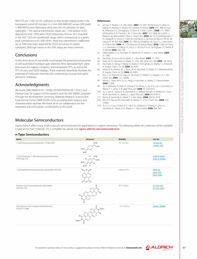
Molecular SemiconductorsSigma-Aldrich offers many small molecule semiconductors for applications in organic electronics. The following tables list a selection of the available n-type and p-type materials. For a complete list, please visit sigma-aldrich.com/semiconductors
n-Type SemiconductorsName Structure Mobility Cat. No.
7,7,8,8-Tetracyanoquinodimethane (TCNQ), 98% C
C
C
CN
N
N
N
10−5 cm2/V·s 157635-5G157635-10G
2,3,5,6-Tetrafluoro-7,7,8,8-tetracyanoquinodimethane (F4TCNQ), 97%
C
C
C
C
N
NN
FF
FF
N
- 376779-25MG376779-100MG
1,4,5,8-Naphthalenetetracarboxylic dianhydride (NTCDA) O OO
OO O
0.003 cm2/V·s N818-5GN818-25GN818-100G
Perylene-3,4,9,10-tetracarboxylic dianhydride (PTCDA), 97%
O
O
O
O
O
O 10−4 cm2/V·s P11255-25GP11255-100G
N,N’-Dipentyl-3,4,9,10-perylenedicarboximide (PTCDI-C5), 98%
N
N
O
O
O
O
C5H11
C5H11
~10−2 cm2/V·s 663921-500MG
TO ORDER: Contact your local Sigma-Aldrich office (see back cover), or visit sigma-aldrich.com/matsci.sigma-aldrich.com68
Self-
Asse
mbl
ed N
anod
iele
ctric
s (SA
ND
s) fo
r Unc
onve
ntio
nal E
lect
roni
cs
Name Structure Mobility Cat. No.
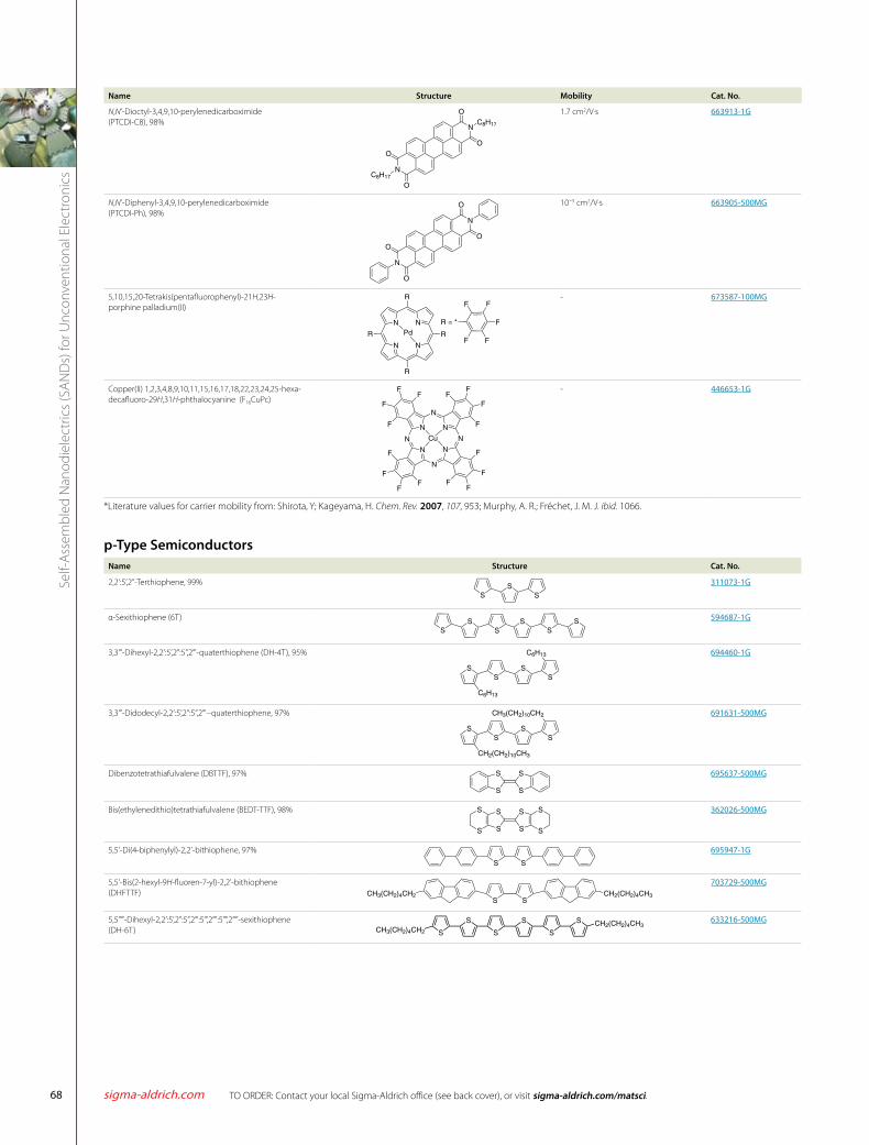
N,N’-Dioctyl-3,4,9,10-perylenedicarboximide (PTCDI-C8), 98%
N
N
O
O
O
O
C8H17
C8H17
1.7 cm2/V·s 663913-1G
N,N’-Diphenyl-3,4,9,10-perylenedicarboximide (PTCDI-Ph), 98%
N
N
O
O
O
O
10−5 cm2/V·s 663905-500MG
5,10,15,20-Tetrakis(pentafluorophenyl)-21H,23H- porphine palladium(II)
N
NN
N
R
R
R
R
R = *
F F
FF
FPd
- 673587-100MG
Copper(II) 1,2,3,4,8,9,10,11,15,16,17,18,22,23,24,25-hexa-decafluoro-29H,31H-phthalocyanine (F16CuPc)
N
N
N
N
N
N
N
N
Cu
F
F F
F
F
FF
F
F F
FF
F
F F
F
- 446653-1G
*Literature values for carrier mobility from: Shirota, Y; Kageyama, H. Chem. Rev. 2007, 107, 953; Murphy, A. R.; Fréchet, J. M. J. ibid. 1066.
p-Type SemiconductorsName Structure Cat. No.
2,2’:5’,2’’-Terthiophene, 99%S
SS
311073-1G
α-Sexithiophene (6T)S
SS
SS
S 594687-1G
3,3’’’-Dihexyl-2,2’:5’,2’’:5’’,2’’’-quaterthiophene (DH-4T), 95%
SS S
S
C6H13
C6H13 694460-1G
3,3’’’-Didodecyl-2,2’:5’,2’’:5’’,2’’’−quaterthiophene, 97%
SS S
S
CH2(CH2)10CH3
CH3(CH2)10CH2 691631-500MG
Dibenzotetrathiafulvalene (DBTTF), 97%
S
S
S
S 695637-500MG
Bis(ethylenedithio)tetrathiafulvalene (BEDT-TTF), 98%
S
S
S
S
S
S
S
S 362026-500MG
5,5’-Di(4-biphenylyl)-2,2’-bithiophene, 97%S S
695947-1G
5,5’-Bis(2-hexyl-9H-fluoren-7-yl)-2,2’-bithiophene (DHFTTF) CH3(CH2)4CH2
SCH2(CH2)4CH3
S
703729-500MG
5,5’’’’’-Dihexyl-2,2’:5’,2’’:5’’,2’’’:5’’’,2’’’’:5’’’’,2’’’’’-sexithiophene (DH-6T) S S
S S S
SCH2(CH2)4CH3
CH3(CH2)4CH2
633216-500MG
For questions, product data, or new product suggestions, please contact Aldrich Materials Science at [email protected]. 69
Self-Assembled N
anodielectrics (SAND
s) for Unconventional Electronics
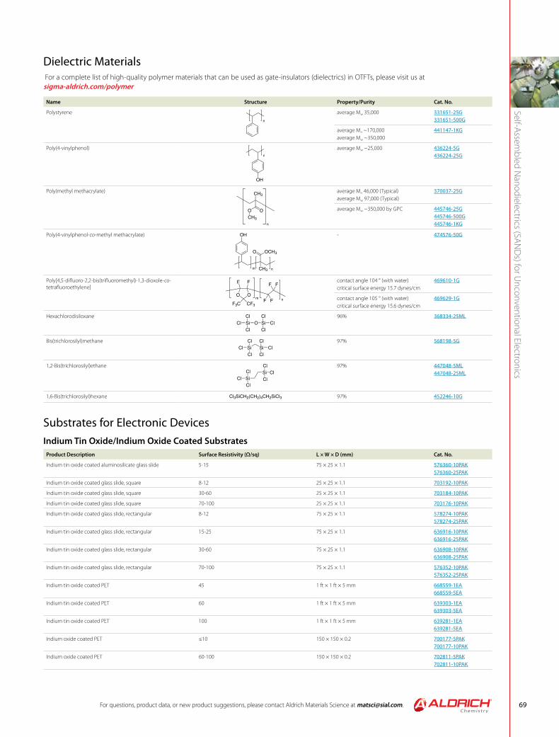
Dielectric Materials For a complete list of high-quality polymer materials that can be used as gate-insulators (dielectrics) in OTFTs, please visit us at sigma-aldrich.com/polymer
Name Structure Property/Purity Cat. No.
Polystyrenen
average Mw 35,000 331651-25G331651-500G
average Mn ~170,000average Mw ~350,000
441147-1KG
Poly(4-vinylphenol)
OH
n
average Mw ~25,000 436224-5G436224-25G
Poly(methyl methacrylate) CH3
O OCH3
n
average Mn 46,000 (Typical)average Mw 97,000 (Typical)
370037-25G
average Mw ~350,000 by GPC 445746-25G445746-500G445746-1KG
Poly(4-vinylphenol-co-methyl methacrylate)
CH3
O OCH3
m n
OH - 474576-50G
Poly[4,5-difluoro-2,2-bis(trifluoromethyl)-1,3-dioxole-co-tetrafluoroethylene]
O O
FF
CF3F3CFF
FF
m n
contact angle 104 ° (with water)critical surface energy 15.7 dynes/cm
469610-1G
contact angle 105 ° (with water)critical surface energy 15.6 dynes/cm
469629-1G
HexachlorodisiloxaneCl Si
Cl
ClO Si
Cl
ClCl
96% 368334-25ML
Bis(trichlorosilyl)methaneSi Si ClCl
ClCl
Cl
Cl 97% 568198-5G
1,2-Bis(trichlorosilyl)ethane
SiClCl
Cl SiCl
ClCl
97% 447048-5ML447048-25ML
1,6-Bis(trichlorosilyl)hexane Cl3SiCH2(CH2)4CH2SiCl3 97% 452246-10G
Substrates for Electronic DevicesIndium Tin Oxide/Indium Oxide Coated Substrates
Product Description Surface Resistivity (Ω/sq) L × W × D (mm) Cat. No.
Indium tin oxide coated aluminosilicate glass slide 5-15 75 × 25 × 1.1 576360-10PAK576360-25PAK
Indium tin oxide coated glass slide, square 8-12 25 × 25 × 1.1 703192-10PAK
Indium tin oxide coated glass slide, square 30-60 25 × 25 × 1.1 703184-10PAK
Indium tin oxide coated glass slide, square 70-100 25 × 25 × 1.1 703176-10PAK
Indium tin oxide coated glass slide, rectangular 8-12 75 × 25 × 1.1 578274-10PAK578274-25PAK
Indium tin oxide coated glass slide, rectangular 15-25 75 × 25 × 1.1 636916-10PAK636916-25PAK
Indium tin oxide coated glass slide, rectangular 30-60 75 × 25 × 1.1 636908-10PAK636908-25PAK
Indium tin oxide coated glass slide, rectangular 70-100 75 × 25 × 1.1 576352-10PAK576352-25PAK
Indium tin oxide coated PET 45 1 ft × 1 ft × 5 mm 668559-1EA668559-5EA
Indium tin oxide coated PET 60 1 ft × 1 ft × 5 mm 639303-1EA639303-5EA
Indium tin oxide coated PET 100 1 ft × 1 ft × 5 mm 639281-1EA639281-5EA
Indium oxide coated PET ≤10 150 × 150 × 0.2 700177-5PAK700177-10PAK
Indium oxide coated PET 60-100 150 × 150 × 0.2 702811-5PAK702811-10PAK
TO ORDER: Contact your local Sigma-Aldrich office (see back cover), or visit sigma-aldrich.com/matsci.sigma-aldrich.com70
Poly
tria
ryla
min
e Se
mic
ondu
ctor
s
Iain McCulloch and Martin Heeney Flexink Limited - www.flexink.co.uk Southampton, UK E-mail: [email protected]
Application of Solution Processable Organic Semiconductors in Organic ElectronicsOrganic electronics is an emerging scientific field of potentially huge technological and commercial relevance1, and is an increasingly ubiquitous research activity globally. One important area is the development of organic field effect transistors (OFET) which can potentially be employed in applications such as RFID tags and display backplanes.2,3 In order to be commercially competitive, these devices must be printed by a low-cost, high throughput process. Additive solution based printing techniques such as ink-jet and contact printing are considered to be attractive processing options. In order to satisfy these printing requirements, the semiconductor material should be formulated into an ink, with appropriate rhelology. There are several potentially high performing semiconductors that have been disclosed in the literature recently that can be deposited from solution into thin films.4-7 In almost all cases, however, aggressive and environmentally unfriendly solvents are required to fully dissolve these crystalline polymers, without which potentially difficult suspensions or gels can form.8 Additionally, the device fabrication process typically requires a pre-treatment step to reduce the energy of the coating surface, as well as a thermal annealing step after semiconductor deposition to induce optimal crystallinity.9 Both these additional steps potentially add cost to the process. Another drawback with some thiophene based polymers is that the high electron density over extended conjugation lengths leads to high lying HOMO energy levels with corresponding susceptibility to electrochemical oxidation in ambient conditions. Even in situations where acceptable ambient stability is demonstrated in storage conditions, devices that are driven at high current density conditions or where a bottom-gate transistor architecture is employed, where the semiconductor film is the exposed surface, suffer from instabilities. These instabilities manifest as a deterioration in the large initial carrier mobilities to significantly lower values over short periods.10 Clearly then, there is a demand for fully air stable polymers that can be easily deposited from environmentally friendly solvents, do not require further treatment to obtain optimal performance and have the flexibility to be employed in any device architecture. Polytriarylamines fit these requirements: they are highly soluble, amorphous semiconducting polymers11 which require no annealing and can achieve stable charge carrier mobilities of the order of 5 x 10⁻³ cm2/Vs in both top and bottom gate transistor architectures.12 The presence of the amine nitrogen in the polymer backbone acts to prevent efficient delocalization of π electrons between adjacent phenyl units, thus limiting the effective conjugation length and resulting in low lying HOMO energy levels and excellent
oxidative stability. The non-planar, rotationally-free and large linkage angle backbone however prevents optimal intermolecular π-electron aromatic stacking, leading to an amorphous microstructure and limiting the charge carrier mobility to lower values than some highly ordered crystalline materials. However, this ease of processing and robust electrical performance offers significant compensation.
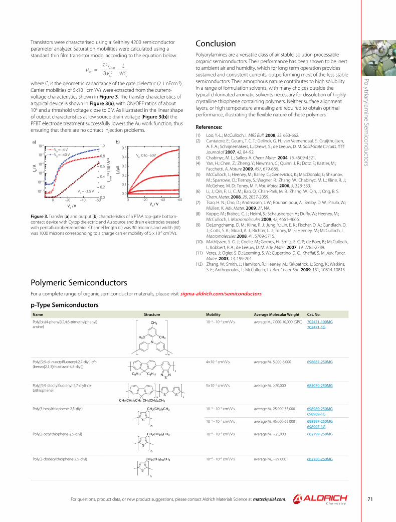
SynthesisPoly(bis(4-phenyl)(2,4,6-trimethylphenyl)amine) (Aldrich Prod. No. 702471) was synthesised by palladium catalysed Suzuki coupling, as shown in Figure 1. To eliminate the effects of unbalanced stoichiometry, a homo-condensation reaction was employed with the asymmetrically bifunctionalized bromo boronate of the triarylamine repeat unit. Purification of the crude polymer is essential, affording the polymer as yellow solid, soluble in common organic solvents such as tolulene (Aldrich Prod. No. 568821), chloroform (Aldrich Prod. No. 372978) and xylene (Aldrich Prod. No. 296333). Number average molecular weights of over 45 Kda can be obtained by this procedure, with polydispersities of between 2 and 3.
N
Br Br
N
Br BO
O+
OB
OO N
n
Figure 1. Synthesis of Poly(bis(4-phenyl)(2,4,6-trimethylphenyl)amine) by palladium catalyzed Suzuki coupling.
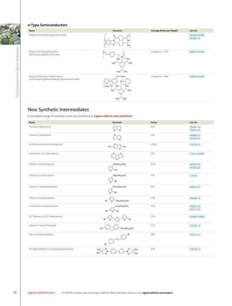
Transistor DevicesField effect transistor devices were fabricated on a glass substrate (Corning EAGLE 2000) using a bottom-contact, top-gate architecture, often referred to as a staggered geometry, as shown in Figure 2. The glass was cleaned by sonication in a detergent solution. Source and drain electrodes were evaporated Au treated with a pentafluorobenzenethiol (PFBT) (Aldrich Prod. No. P3033) self-assembled monolayer. Typical channel dimensions were 30 µm length and 1000 µm width. Polymers were spin coated from a 10 mg/ml solution in chlorobenzene at 2000 rpm and dried at 100°C for 2 min. The gate dielectric was a fluoropolymer CYTOP and again deposited by spin coating from a 9 wt% solution in FC43 solvent, and dried at 100°C. Top-gate electrodes were evaporated aluminum. Device fabrication was carried out under nitrogen with storage and electrical testing in air for the stability tests.
Gate Electrode
Dielectric
Semiconductor
Source Gate
Substrate
Passivation Layer
Figure 2. Top gate, staggered contact transistor architecture
Polytriarylamine Semiconductors
For questions, product data, or new product suggestions, please contact Aldrich Materials Science at [email protected]. 71
Polytriarylamine Sem
iconductors
Transistors were characterised using a Keithley 4200 semiconductor parameter analyzer. Saturation mobilities were calculated using a standard thin film transistor model according to the equation below:
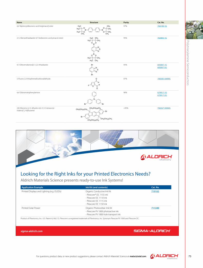
WCi
L∂ VG
2
∂ 2 IDsat=µsat
where Ci is the geometric capacitance of the gate dielectric (2.1 nFcm-2). Carrier mobilities of 5x10⁻³ cm2/Vs were extracted from the current-voltage characteristics shown in Figure 3. The transfer characteristics of a typical device is shown in Figure 3(a), with ON/OFF ratios of about 104 and a threshold voltage close to 0 V. As illustrated in the linear shape of output characteristics at low source drain voltage (Figure 3(b)) the PFBT electrode treatment successfully lowers the Au work function, thus ensuring that there are no contact injection problems.
0 -20 -40 -60
10-11
10-10
10-9
10-8
10-7
10-6
0.0
0.2
0.4
0.6
0.8
1.0 VD = -4 V VD = -40 V
I D / A
VG / V
I D s
at1/
2 / 1
0-3 A
1/2
VT = -3.5 V
0 -20 -40 -60
0.0
0.1
0.2
0.3
0.4
0.5
VG: 0 to -60V
I D/µ
A
VD / V
a) b)
Figure 3. Transfer (a) and output (b) characteristics of a PTAA top-gate bottom-contact device with Cytop dielectric and Au source and drain electrodes treated with pentafluorobenzenethiol. Channel length (L) was 30 microns and width (W) was 1000 microns corresponding to a charge carrier mobility of 5 x 10⁻³ cm2/Vs.
ConclusionPolyarylamines are a versatile class of air stable, solution processable organic semiconductors. Their performance has been shown to be inert to ambient air and humidity, which for long term operation provides sustained and consistent currents, outperforming most of the less stable semiconductors. Their amorphous nature contributes to high solubility in a range of formulation solvents, with many choices outside the typical chlorinated aromatic solvents necessary for dissolution of highly crystalline thiophene containing polymers. Neither surface alignment layers, or high temperature annealing are required to obtain optimal performance, illustrating the flexible nature of these polymers.
References:(1) Loo, Y.-L.; McCulloch, I. MRS Bull. 2008, 33, 653-662. (2) Cantatore, E.; Geuns, T. C. T.; Gelinck, G. H.; van Veenendaal, E.; Gruijthuijsen,
A. F. A.; Schrijnemakers, L.; Drews, S.; de Leeuw, D. M. Solid-State Circuits, IEEE Journal of 2007, 42, 84-92.
(3) Chabinyc, M. L.; Salleo, A. Chem. Mater. 2004, 16, 4509-4521. (4) Yan, H.; Chen, Z.; Zheng, Y.; Newman, C.; Quinn, J. R.; Dotz, F.; Kastler, M.;
Facchetti, A. Nature 2009, 457, 679-686. (5) McCulloch, I.; Heeney, M.; Bailey, C.; Genevicius, K.; MacDonald, I.; Shkunov,
M.; Sparrowe, D.; Tierney, S.; Wagner, R.; Zhang, W.; Chabinyc, M. L.; Kline, R. J.; McGehee, M. D.; Toney, M. F. Nat. Mater. 2006, 5, 328-333.
(6) Li, J.; Qin, F.; Li, C. M.; Bao, Q.; Chan-Park, M. B.; Zhang, W.; Qin, J.; Ong, B. S. Chem. Mater. 2008, 20, 2057-2059.
(7) Tsao, H. N.; Cho, D.; Andreasen, J. W.; Rouhanipour, A.; Breiby, D. W.; Pisula, W.; Müllen, K. Adv. Mater. 2009, 21, NA.
(8) Koppe, M.; Brabec, C. J.; Heiml, S.; Schausberger, A.; Duffy, W.; Heeney, M.; McCulloch, I. Macromolecules 2009, 42, 4661-4666.
(9) DeLongchamp, D. M.; Kline, R. J.; Jung, Y.; Lin, E. K.; Fischer, D. A.; Gundlach, D. J.; Cotts, S. K.; Moad, A. J.; Richter, L. J.; Toney, M. F.; Heeney, M.; McCulloch, I. Macromolecules 2008, 41, 5709-5715.
(10) Mathijssen, S. G. J.; Coelle, M.; Gomes, H.; Smits, E. C. P.; de Boer, B.; McCulloch, I.; Bobbert, P. A.; de Leeuw, D. M. Adv. Mater. 2007, 19, 2785-2789.
(11) Veres, J.; Ogier, S. D.; Leeming, S. W.; Cupertino, D. C.; Khaffaf, S. M. Adv. Funct. Mater. 2003, 13, 199-204.
(12) Zhang, W.; Smith, J.; Hamilton, R.; Heeney, M.; Kirkpatrick, J.; Song, K.; Watkins, S. E.; Anthopoulos, T.; McCulloch, I. J. Am. Chem. Soc. 2009, 131, 10814-10815.
Polymeric SemiconductorsFor a complete range of organic semiconductor materials, please visit sigma-aldrich.com/semiconductors
p-Type SemiconductorsName Structure Mobility Average Molecular Weight Cat. No.
Poly[bis(4-phenyl)(2,4,6-trimethylphenyl)amine]
N
CH3
CH3H3C
n
10−3 - 10−2 cm2/V·s average Mn 7,000-10,000 (GPC) 702471-100MG702471-1G
Poly[(9,9-di-n-octylfluorenyl-2,7-diyl)-alt-(benzo[2,1,3]thiadiazol-4,8-diyl)]
C8H17 C8H17n
NS
N
4×10⁻³ cm2/V·s average Mn 5,000-8,000 698687-250MG
Poly[(9,9-dioctylfluorenyl-2,7-diyl)-co-bithiophene]
CH3(CH2)6CH2 CH2(CH2)6CH3
S Sm n
5×10⁻³ cm2/V·s average Mn >20,000 685070-250MG
Poly(3-hexylthiophene-2,5-diyl)
S
CH2(CH2)4CH3
n
10−4 - 10−1 cm2/V·s average Mn 25,000-35,000 698989-250MG698989-1G
10−4 - 10−1 cm2/V·s average Mn 45,000-65,000 698997-250MG698997-1G
Poly(3-octylthiophene-2,5-diyl)
S
CH2(CH2)6CH3
n
10−4 - 10−1 cm2/V·s average Mn ~25,000 682799-250MG
Poly(3-dodecylthiophene-2,5-diyl)
S
CH2(CH2)10CH3
n
10−4 - 10−1 cm2/V·s average Mw ~27,000 682780-250MG
TO ORDER: Contact your local Sigma-Aldrich office (see back cover), or visit sigma-aldrich.com/matsci.sigma-aldrich.com72
Poly
tria
ryla
min
e Se
mic
ondu
ctor
s
n-Type SemiconductorsName Structure Average Molecular Weight Cat. No.
Poly(benzimidazobenzophenanthroline)
NN
N
OO
Nn
- 667846-250MG667846-1G
Poly[(1,4-divinylenephenylene)(2,4,6-triisopropylphenylborane)]
B
H3C CH3
CH3
CH3H3C
CH3n
average Mn ~1379 688010-250MG
Poly[(2,5-didecyloxy-1,4-phenylene) (2,4,6-triisopropylphenylborane)], diphenyl terminated
O
OC10H21
C10H21
B
CH3
CH3
CH3
H3C
H3C CH3
n
average Mn ~1446 688002-250MG
New Synthetic IntermediatesA complete range of synthetic tools can be found at sigma-aldrich.com/synthetic
Name Structure Purity Cat. No.
Thieno[2,3-b]thiophene
SS
95% 702641-1G702641-5G
Thieno[3,2-b]thiophene
S
S 95% 702668-1G702668-5G
2,5-Dibromothieno[3,2-b]thiophene
S
SBrBr
≥98% 710164-1G
Dithieno[3,2-b:2’,3’-d]thiophene
S
SS 97% 710172-500MG
2-Bromo-3-hexylthiophene
S Br
CH2(CH2)4CH3 97% 691925-1G691925-5G
2-Bromo-3-octylthiophene
S Br
CH2(CH2)6CH3 97% 714550
2-Bromo-3-dodecylthiophene
S
CH2(CH2)10CH3
Br
95% 688312-1G
5-Bromo-2-hexylthiopheneSBr CH2(CH2)4CH3
97% 694258-1G
2,5-Dibromo-3-hexylthiophene
SBr Br
CH2(CH2)4CH3 97% 456373-1G456373-5G
5,5’’-Dibromo-2,2’:5’,2’’-terthiopheneS
SSBr Br
97% 699098-500MG
2-Bromo-7-hexyl-9H-fluoreneBr CH2(CH2)4CH3
97% 701254-1G
trans-4,4’-Dibromostilbene
Br
Br 98% 705721-1G
4,4’-biphenyldiboronic acid bis(neopentyl) esterBB
O
OO
O
CH3
CH3
H3C
H3C
97% 704318-1G
For questions, product data, or new product suggestions, please contact Aldrich Materials Science at [email protected]. 73
Polytriarylamine Sem
iconductors
Name Structure Purity Cat. No.
4,4’-Biphenyldiboronic acid bis(pinacol) ester
BO
O CH3CH3
CH3
CH3BO
OH3CCH3
H3C
H3C
97% 704199-1G
2,1,3-Benzothiadiazole-4,7-bis(boronic acid pinacol ester)
NS
N
B
B
OO
O O
H3CH3C
CH3
CH3
H3C
H3C
CH3
CH3
95% 702803-1G
4,7-Dibromobenzo[c]-1,2,5-thiadiazole
NS
N
Br
Br 95% 693847-1G693847-5G
5-Fluoro-2,3-thiophenedicarboxaldehyde
S
HH
O
O
F
97% 708283-500MG
4,4’-Dibromotriphenylamine
N
Br Br
96% 679917-1G679917-5G
2,8-Dibromo-6,12-dihydro-6,6,12,12-tetraoctyl- indeno[1,2-b]fluorene
CH2(CH2)6CH3CH3(CH2)6CH2
CH3(CH2)6CH2CH2(CH2)6CH3
Br
Br
>95% 708267-500MG
sigma-aldrich.com
Looking for the Right Inks for your Printed Electronics Needs? Aldrich Materials Science presents ready-to-use Ink Systems!
Application Example Ink Kit (and contents) Cat. No.
Printed Displays and Lighting (e.g. OLEDs) Organic Conductive Ink Kit - Plexcore® OC 1155 ink - Plexcore OC 1110 ink - Plexcore OC 1115 ink - Plexcore OC 1150 ink
719102
Printed Solar Power Organic Photovoltaic Ink Kit - Plexcore PV 1000 photoactive ink - Plexcore PV 1000 hole transport ink
711349
Product of Plextronics, Inc. U.S. Patent 6,166,172. Plexcore is a registered trademark of Plextronics, Inc. Synonym Plexcore PV 1000 and Plexcore OC.
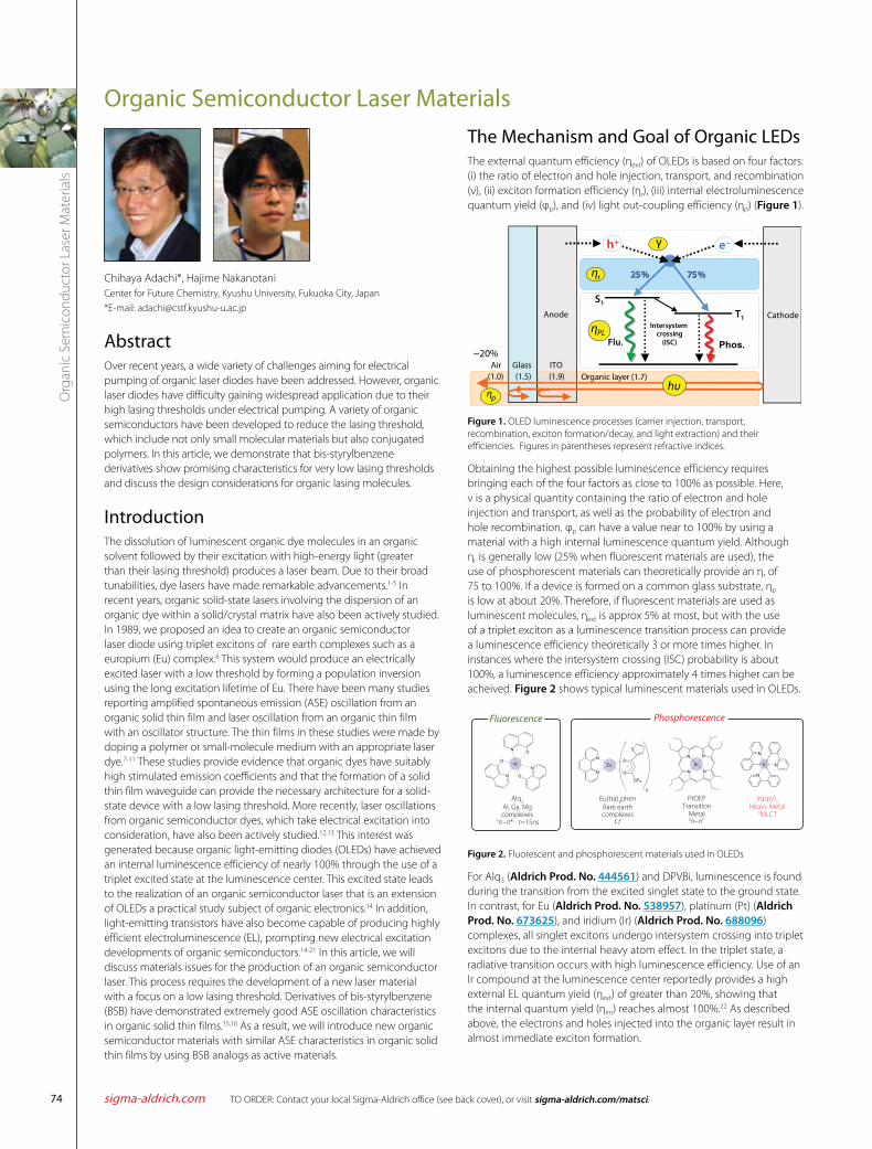
TO ORDER: Contact your local Sigma-Aldrich office (see back cover), or visit sigma-aldrich.com/matsci.sigma-aldrich.com74
Org
anic
Sem
icon
duct
or L
aser
Mat
eria
ls
Chihaya Adachi*, Hajime Nakanotani Center for Future Chemistry, Kyushu University, Fukuoka City, Japan *E-mail: [email protected]
AbstractOver recent years, a wide variety of challenges aiming for electrical pumping of organic laser diodes have been addressed. However, organic laser diodes have difficulty gaining widespread application due to their high lasing thresholds under electrical pumping. A variety of organic semiconductors have been developed to reduce the lasing threshold, which include not only small molecular materials but also conjugated polymers. In this article, we demonstrate that bis-styrylbenzene derivatives show promising characteristics for very low lasing thresholds and discuss the design considerations for organic lasing molecules.
IntroductionThe dissolution of luminescent organic dye molecules in an organic solvent followed by their excitation with high-energy light (greater than their lasing threshold) produces a laser beam. Due to their broad tunabilities, dye lasers have made remarkable advancements.1-5 In recent years, organic solid-state lasers involving the dispersion of an organic dye within a solid/crystal matrix have also been actively studied. In 1989, we proposed an idea to create an organic semiconductor laser diode using triplet excitons of rare earth complexes such as a europium (Eu) complex.6 This system would produce an electrically excited laser with a low threshold by forming a population inversion using the long excitation lifetime of Eu. There have been many studies reporting amplified spontaneous emission (ASE) oscillation from an organic solid thin film and laser oscillation from an organic thin film with an oscillator structure. The thin films in these studies were made by doping a polymer or small-molecule medium with an appropriate laser dye.7-11 These studies provide evidence that organic dyes have suitably high stimulated emission coefficients and that the formation of a solid thin film waveguide can provide the necessary architecture for a solid-state device with a low lasing threshold. More recently, laser oscillations from organic semiconductor dyes, which take electrical excitation into consideration, have also been actively studied.12,13 This interest was generated because organic light-emitting diodes (OLEDs) have achieved an internal luminescence efficiency of nearly 100% through the use of a triplet excited state at the luminescence center. This excited state leads to the realization of an organic semiconductor laser that is an extension of OLEDs a practical study subject of organic electronics.14 In addition, light-emitting transistors have also become capable of producing highly efficient electroluminescence (EL), prompting new electrical excitation developments of organic semiconductors.14-21 In this article, we will discuss materials issues for the production of an organic semiconductor laser. This process requires the development of a new laser material with a focus on a low lasing threshold. Derivatives of bis-styrylbenzene (BSB) have demonstrated extremely good ASE oscillation characteristics in organic solid thin films.15,16 As a result, we will introduce new organic semiconductor materials with similar ASE characteristics in organic solid thin films by using BSB analogs as active materials.
The Mechanism and Goal of Organic LEDsThe external quantum efficiency (ηext) of OLEDs is based on four factors: (i) the ratio of electron and hole injection, transport, and recombination (ν), (ii) exciton formation efficiency (ηr), (iii) internal electroluminescence quantum yield (φp), and (iv) light out-coupling efficiency (ηp) (Figure 1).
Anode Cathode
γ
ηp
ηPL
ITO(1.9)
Glass(1.5)
Air(1.0)
Intersystem crossing
(ISC)
S1
T1
Phos.Flu.
75%75%25%25%
hυ
e–e–h+h+
ηr
~20%
Organic layer (1.7)
Figure 1. OLED luminescence processes (carrier injection, transport, recombination, exciton formation/decay, and light extraction) and their efficiencies. Figures in parentheses represent refractive indices.
Obtaining the highest possible luminescence efficiency requires bringing each of the four factors as close to 100% as possible. Here, ν is a physical quantity containing the ratio of electron and hole injection and transport, as well as the probability of electron and hole recombination. φp can have a value near to 100% by using a material with a high internal luminescence quantum yield. Although ηr is generally low (25% when fluorescent materials are used), the use of phosphorescent materials can theoretically provide an ηr of 75 to 100%. If a device is formed on a common glass substrate, ηp is low at about 20%. Therefore, if fluorescent materials are used as luminescent molecules, ηext is approx 5% at most, but with the use of a triplet exciton as a luminescence transition process can provide a luminescence efficiency theoretically 3 or more times higher. In instances where the intersystem crossing (ISC) probability is about 100%, a luminescence efficiency approximately 4 times higher can be acheived. Figure 2 shows typical luminescent materials used in OLEDs.
N
N
N
O
O
Al
O
Alq3Al, Ga, Mgcomplexes
1π−π* τ=15ns
N
N
S
O
O
CF3
3
Eu
Eu(tta)3phenRare earthcomplexes
f-f
N
NN
N
Pt
PtOEPTransition
Metal3π−π*
N
Ir
N
N
Ir(ppy)3Heavy Metal
3MLCT
Fluorescence Phosphorescence
Figure 2. Fluorescent and phosphorescent materials used in OLEDs
For Alq3 (Aldrich Prod. No. 444561) and DPVBi, luminescence is found during the transition from the excited singlet state to the ground state. In contrast, for Eu (Aldrich Prod. No. 538957), platinum (Pt) (Aldrich Prod. No. 673625), and iridium (Ir) (Aldrich Prod. No. 688096) complexes, all singlet excitons undergo intersystem crossing into triplet excitons due to the internal heavy atom effect. In the triplet state, a radiative transition occurs with high luminescence efficiency. Use of an Ir compound at the luminescence center reportedly provides a high external EL quantum yield (ηext) of greater than 20%, showing that the internal quantum yield (ηint) reaches almost 100%.22 As described above, the electrons and holes injected into the organic layer result in almost immediate exciton formation.
Organic Semiconductor Laser Materials
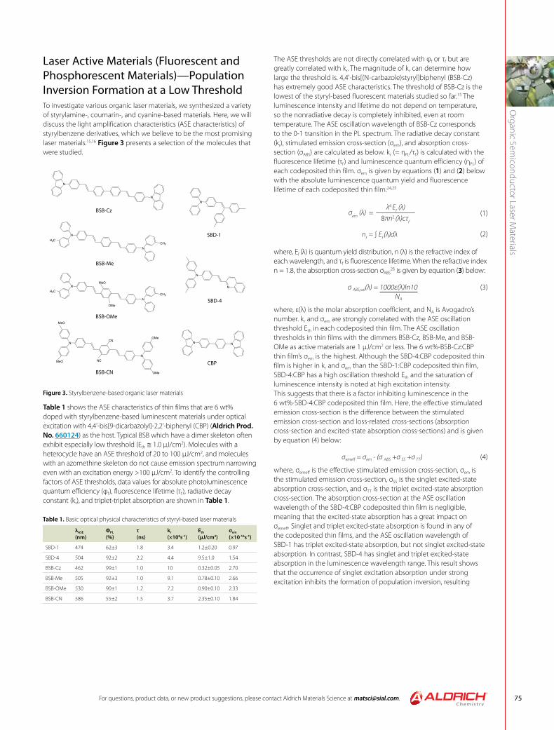
For questions, product data, or new product suggestions, please contact Aldrich Materials Science at [email protected]. 75
Organic Sem
iconductor Laser Materials
Laser Active Materials (Fluorescent and Phosphorescent Materials)—Population Inversion Formation at a Low ThresholdTo investigate various organic laser materials, we synthesized a variety of styrylamine-, coumarin-, and cyanine-based materials. Here, we will discuss the light amplification characteristics (ASE characteristics) of styrylbenzene derivatives, which we believe to be the most promising laser materials.15,16 Figure 3 presents a selection of the molecules that were studied.
N
N
BSB-Cz
N
N
H3CCH3
BSB-Me
N
N
H3CCH3
MeO
OMe
BSB-OMe
N
N
OMe
OMe
CN
MeO
MeO NC
BSB-CN
N
SBD-1
N
N
SBD-4
N N
CBP
Figure 3. Styrylbenzene-based organic laser materials
Table 1 shows the ASE characteristics of thin films that are 6 wt% doped with styrylbenzene-based luminescent materials under optical excitation with 4,4’-bis[9-dicarbazolyl]-2,2’-biphenyl (CBP) (Aldrich Prod. No. 660124) as the host. Typical BSB which have a dimer skeleton often exhibit especially low threshold (Eth ≅ 1.0 µJ/cm2). Molecules with a heterocycle have an ASE threshold of 20 to 100 µJ/cm2, and molecules with an azomethine skeleton do not cause emission spectrum narrowing even with an excitation energy >100 µJ/cm2. To identify the controlling factors of ASE thresholds, data values for absolute photoluminescence quantum efficiency (φf), fluorescence lifetime (τf), radiative decay constant (kr), and triplet-triplet absorption are shown in Table 1.
Table 1. Basic optical physical characteristics of styryl-based laser materials
λASE
(nm)ΦPL
(%)τ(ns)
kr
(×108s-1)Eth
(µJ/cm2)σem
(×10-16s-1)
SBD-1 474 62±3 1.8 3.4 1.2±0.20 0.97
SBD-4 504 92±2 2.2 4.4 9.5±1.0 1.54
BSB-Cz 462 99±1 1.0 10 0.32±0.05 2.70
BSB-Me 505 92±3 1.0 9.1 0.78±0.10 2.66
BSB-OMe 530 90±1 1.2 7.2 0.90±0.10 2.33
BSB-CN 586 55±2 1.5 3.7 2.35±0.10 1.84
The ASE thresholds are not directly correlated with φf or τf but are greatly correlated with kr. The magnitude of kr can determine how large the threshold is. 4,4’-bis[(N-carbazole)styryl]biphenyl (BSB-Cz) has extremely good ASE characteristics. The threshold of BSB-Cz is the lowest of the styryl-based fluorescent materials studied so far.15 The luminescence intensity and lifetime do not depend on temperature, so the nonradiative decay is completely inhibited, even at room temperature. The ASE oscillation wavelength of BSB-Cz corresponds to the 0-1 transition in the PL spectrum. The radiative decay constant (kr), stimulated emission cross-section (σem), and absorption cross-section (σABS) are calculated as below. kr (= ηPL/τf) is calculated with the fluorescence lifetime (τf) and luminescence quantum efficiency (ηPL) of each codeposited thin film. σem is given by equations (1) and (2) below with the absolute luminescence quantum yield and fluorescence lifetime of each codeposited thin film:24,25
σem (λ) =λ4 Ef (λ)
8πn2 (λ)cτf
(1)
nf = ∫ Ef (λ)dλ (2)
where, Ef (λ) is quantum yield distribution, n (λ) is the refractive index of each wavelength, and τf is fluorescence lifetime. When the refractive index n = 1.8, the absorption cross-section σABS
26 is given by equation (3) below:
σ ABS,sol(λ) = 1000ε(λ)ln10 (3) NA
where, ε(λ) is the molar absorption coefficient, and NA is Avogadro’s number. kr and σem are strongly correlated with the ASE oscillation threshold Eth in each codeposited thin film. The ASE oscillation thresholds in thin films with the dimmers BSB-Cz, BSB-Me, and BSB-OMe as active materials are 1 µJ/cm2 or less. The 6 wt%-BSB-Cz:CBP thin film’s σem is the highest. Although the SBD-4:CBP codeposited thin film is higher in kr and σem than the SBD-1:CBP codeposited thin film, SBD-4:CBP has a high oscillation threshold Eth and the saturation of luminescence intensity is noted at high excitation intensity. This suggests that there is a factor inhibiting luminescence in the 6 wt%-SBD-4:CBP codeposited thin film. Here, the effective stimulated emission cross-section is the difference between the stimulated emission cross-section and loss-related cross-sections (absorption cross-section and excited-state absorption cross-sections) and is given by equation (4) below:
σemeff = σem - (σ ABS +σ SS +σ TT) (4)
where, σemeff is the effective stimulated emission cross-section, σem is the stimulated emission cross-section, σSS is the singlet excited-state absorption cross-section, and σTT is the triplet excited-state absorption cross-section. The absorption cross-section at the ASE oscillation wavelength of the SBD-4:CBP codeposited thin film is negligible, meaning that the excited-state absorption has a great impact on σemeff. Singlet and triplet excited-state absorption is found in any of the codeposited thin films, and the ASE oscillation wavelength of SBD-1 has triplet excited-state absorption, but not singlet excited-state absorption. In contrast, SBD-4 has singlet and triplet excited-state absorption in the luminescence wavelength range. This result shows that the occurrence of singlet excitation absorption under strong excitation inhibits the formation of population inversion, resulting
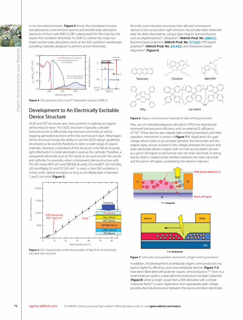
TO ORDER: Contact your local Sigma-Aldrich office (see back cover), or visit sigma-aldrich.com/matsci.sigma-aldrich.com76
Org
anic
Sem
icon
duct
or L
aser
Mat
eria
ls
in no stimulated emission. Figure 4 shows the stimulated emission and absorption cross-sections spectra and excited-state absorption spectrum of the 6 wt%-BSB-Cz:CBP codeposited thin film that has the lowest ASE oscillation threshold. For BSB-Cz, neither the single nor triplet excited-state absorption exists at the ASE oscillation wavelength, providing materials designed to perform at low thresholds.
Abs.
GroundState
S1
Tn
T1
BSB-Cz
Sn
Flu.
600 80010-3
10-2
10-1
100
101 Absorption cross-section
Stimulated emission cross-section
0
1
2
3
4
5
Exci
ted
stat
es a
bsor
ptio
n (a
.u.)
S-S absorption T-T absorption
Wavelength (nm)
σ em a
nd σ
abs (×
10-1
6 cm
2 )
400
Figure 4. ASE spectrum and S-S and T-T absorption spectra of BSB-Cz
Development to An Electrically Excitable Device StructureOLED and FET structures also show promise in realizing an organic semiconductor laser. The OLED structure is basically a double heterostructure to effectively trap electrons and holes as well as trapping generated excitons within the luminescent layer. Advantages of this structure include the ability to use the OLED design guidelines developed so far and the flexibility to select a wide range of organic materials. However, a drawback of this structure is the failure to guide light effectively if a metal electrode is used as the cathode. Therefore, a transparent electrode such as ITO needs to be used at both the anode and cathode. For example, when a transparent device structure with ITO (30 nm)/a-NPD (20 nm)/CBP:BSB [6 wt%] (70 nm)/BCP (20 nm)/Alq3 (20 nm)/MgAg (X nm)/ITO (30 nm)15 is used, a clear ASE oscillation is noted under optical excitation as long as the MgAg layer is between 1 and 3 nm thick (Figure 5).
0 10 20 30 40 50 600
5000
10000
15000
20000
ASE threshold
Input intensity (µJ/cm2)
Emis
sion
Inte
nsity
(a.u
.)
ITO (30nm)
ITO (30nm)
Pumping
CBP:BSB (70nm)
MgAg
α-NPD (20nm)
Alq3 (20nm)BCP (20nm)
9.0±1.8µJ/cm2
Figure 5. ASE characteristics under the excitation of light from an electrically excitable laser structure
Recently, even transistor structures have allowed luminescent devices to be constructed. Light emission has actually been observed near the drain electrode by using p-type organic semiconductors such as oligothiophene27, tetracene28 (Aldrich Prod. No. 698415), fluorene-based polymers (Aldrich Prod. No. 571032), PPV-based polymers29 (Aldrich Prod. No. 541443), and thiophene-based oligomers30 (Figure 6).
Tetracene
n
Fluorene
O
O n
MEH-PPV
TPPy
n-2
9,9'-DAFO
Figure 6. Organic semiconductor materials for light-emitting transistors
Also, use of a tetraphenylpyrene derivative (TPPy) has dramatically improved luminescence efficiency with an external EL efficiency of 1%.31 These devices are unipolar light-emitting transistors, and their operation mechanism is shown in Figure 7-1. Application of a gate voltage allows holes to accumulate between the electrodes and the organic layer, and an increase in the voltage between the source and drain electrodes allows a region with no hole accumulation (known as a pinch-off region) to be formed near the drain electrode. A strong electric field is created at the interface between the drain electrode and the pinch-off region, accelerating the electron injection.
Hole accumulation by Vg
S D
G
7-1: Unipolar
7-2: Ambipolar
Pinch-o� region
Source
SiO2
Drain
+ + + + ++++++
–– – –
– ––
– ––
Figure 7. Schematics and operation mechanisms of light-emitting transistors
In addition, the development of ambipolar organic semiconductors has lead to higher EL efficiency, and some ambipolar devices (Figure 7-2) have been fabricated with polymer organic semiconductors.32,33 Even in a small-molecule system, a clear electroluminescence has been observed (Figure 8) when a single-crystal from a BSB derivative with a simple molecular frame34 is used. Application of an appropriate gate voltage provides electroluminescence between the source and drain electrodes.
For questions, product data, or new product suggestions, please contact Aldrich Materials Science at [email protected]. 77
Organic Sem
iconductor Laser Materials
+
-
Source electrode
Drain electrode
Organic single-crystal
Figure 8. Ambipolar FET producing bright electroluminescence
This ambipolar type architecture also has many advantages over OLEDs and shows promise as a future device structure for organic semiconductor lasers. Transistors using organic substances have been studied since the early 1980s when a pioneering organic transistor was first reported.35 As findings about materials and devices have accumulated rapidly, the use of fused polycyclic aromatic compounds such as tetracene and rubrene (Aldrich Prod. No. 554073) have recently achieved an electron field-effect mobility of about 10 cm2/Vs. Electroluminescence from devices using a transistor structure has a high electronic and optical freedom, and are therefore suitable for organic semiconductor lasers, holding promise for future developments.
References:(1) Sorokin, P. P.; Lankard, J. R. IBM J. Res. Develop. 1966, 10, 162-163. (2) Schäfer, F. P.; Schmidt, W.; Volze, J. Appl. Phys. Lett. 1966, 9, 306 -309. (3) Soffer B. H.; McFarland, B. B. Appl. Phys. Lett. 1967, 10, 266-267. (4) Sorokin, P. P.; Lankard, J. R.; Moruzzi, V. L.; Hammond, E. C. J. Chem. Phys. 1968,
48, 4726-4741. (5) Sorokin, P. P.; Lankard, J. R.; Moruzzi, V. L.; Lurio, A. Appl. Phys. Lett. 1969, 15,
179-181. (6) Chihaya Adachi, Student Advanced technical paper, 1989, Nippon Kogyo
Shinbun
(7) Tessler, N.; Denton, G. J.; Friend, R. H. Nature 1996, 382, 695-697. (8) Frolov, S. V.; Ozaki, M.; Gellermann, W.; Vardeny, Z. V.; Yoshino, K. Jpn. J. Appl.
Phys. 1996, 35, L1371- L1373. (9) Hide, F.; diaz-García, M. A.; Schwartz, B. J.; Andersson, M. R.; Pei, Q.; Heeger, A.
J. Science 1996, 273, 1833-1836. (10) Kozlov, V. G.; Bulovic, V.; Burrows, P. E.; Forrest, S. R.; Nature 1997, 389, 362-364. (11) Berggren, M.; Dodabalapur, A.; Slusher, R. E.; Bao, Z.; Nature 1997, 389,
466-469.(12) Tessler, N. Adv. Mater. 1999, 5, 363-370. (13) Yamamoto, H.; Oyamada, T.; Sasabe, H.; Adachi, C. Appl. Phys. Lett. 84,
1401-1403. (14) Adachi, C.; Baldo, M. A.; Forrest, S. R. J. Appl. Phys. 2001, 90, 5048-8055.(15) Aimono, T.; Kawamura, Y.; Goushi, K.; Yamamoto, H.; Sasabe, H.; Adachi, C.
Appl. Phys. Lett. 2005, 86, 071110-071112. (16) Nakanotani, H.; Sasabe, H.; Adachi, C. Proc. SPIE Int. Soc. Opt. Eng. 2005, 5937,
59370W-1-7. (17) Yamamoto, H.; Kasajima, H.; Yokoyama, W.; Sasabe, H.; Adachi, C. Appl. Phys.
Lett. 2005, 86, 083502-083504. (18) Nakanotani, H.; Oyamada, T.; Kawamura, Y.; Sasabe, H.; Adachi, C. Jpn. J. Appl.
Phys. 2005, 44, 3659-3662.(19) Baldo, M. A.; Adachi, C.; Forrest, S. R. Phys. Rev. B 2000, 62, 109671-10977. (20) Baldo, M. A.; Holmes, R. J.; Forrest, S. R. Phys. Rev. B 2002, 66, 035321. (21) Nakanotani, N.; Sasabe, H.; Adachi, C. Appl. Phys. Lett. 2005, 86, 213506-1-3. (22) Adachi, C.; Baldo M. A.; Forrest, S. R. J. Appl. Phys. 2001, 90, 5048-5051. (23) Yokoyama, W.; Sasabe, H.; Adachi, C. Jpn. J. Appl. Phys. 2003, 42, L1353-1355. (24) Deshpande, A.; Deshpande, V.; Beidoun, A.; Penzkofer, A.; Wagenblast, G.
Chem. Phys. 1990, 142, 123-131. (25) Holzer, W.; Penzkofer, A.; Schmitt, T.; Hartmann, A.; Bader, C.; Tillmann, H.;
Raabe, D.; Stockmann, R.; Hörhold, H.-H. Opt. Quantum Electron 2001, 33, 121-150.
(26) Liu, X.; Py, C.; Tao, Y.; Li, Y.; Ding, J.; Day, M. Appl. Phys. Lett. 2004, 84, 2727-2729. (27) Shaklee K. L.; Leheny, R. F. Appl. Phys. Lett. 1971, 18, 475-305. (28) Schön, J. H.; Kloc, Ch.; Haddon R. C.; Batlogg, B. Science 2000, 288, 656-658. (29) Hepp, A.; Heil, H.; Weise, W.; Ahles, M.; Schmechel, R.; von Seggern, H. Phys.
Rev. Lett. 2003, 91, 157406-1-4. (30) Sakanoue, T.; Fujiwara, E.; Yamada R.; Tada, H. Appl. Phys. Lett. 2004, 84,
3037-3039. (31) Oyamada, T.; Okuyama, S.; Shimoji, N.; Matsushige, K.; Sasabe, H.; Adachi, C.
Appl. Phys. Lett. 2005, 86, 093505. (32) Oyamada, T.; Uchiuzo, H.; Akiyama, S.; Oku, Y.; Shimoji, N.; Matsushige, K.;
Sasabe, H.; Adachi, C. J. Appl. Phys. 2005, 98, 074506-1-7. (33) Zaumseil, J.; Friend, R. H.; Sirringhaus, H. Nature Materials 2006, 5, 69-74. (34) Dinelli, F.; Capelli, R.; Loi, M. A.; Murgia, M.; Muccini, M.; Facchetti A.; Marks, T. J.
Adv. Mat. 2006, 18, 1416-1420. (35) Nakanotani, H.; Saito, M.; Nakamura H.; Adachi, C. Appl. Phys. Lett. 2009, 95,
033308. (36) Kudo, K.; Yamashina, M.; Moriizumi, T. Jpn. J. Appl. Phys. 1984, 23, 130.
Sublimed Grade Materials for Organic ElectronicsName Structure Purity Spectroscopic Properties Cat. No.
Anthracene sublimed grade ≥99% - 694959-5G694959-25G
Benz[b]anthracene sublimed grade 99.99% trace metals basis
λmax = 277 nmλem = 481, 514 nm in dichloromethane-d2
698415-1G
Perylene sublimed grade ≥99.5% λmax = 436 nmλem = 447 nm in tetrahydrofuran
394475-1G394475-5G
4,4’-Bis(N-carbazolyl)-1,1’-biphenyl
NN
sublimed grade ≥99.99% trace metals basis
λmax = 532 nm 699195-1G
N,N’-Di-[(1-naphthyl)-N,N’-diphenyl]-1,1’-biphenyl)-4,4’-diamine
N N
sublimed grade 99% - 556696-500MG
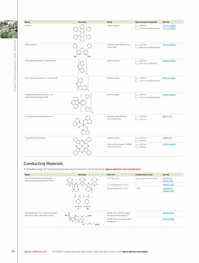
TO ORDER: Contact your local Sigma-Aldrich office (see back cover), or visit sigma-aldrich.com/matsci.sigma-aldrich.com78
Org
anic
Sem
icon
duct
or L
aser
Mat
eria
ls
Name Structure Purity Spectroscopic Properties Cat. No.
Rubrene sublimed grade λmax = 299 nmλem = 550 nm in tetrahydrofuran
551112-100MG551112-500MG
Bathocuproine
N NH3C CH3
sublimed grade 99.99% trace metals basis
λmax = 277 nmλem = 386 nm in tetrahydrofuran
699152-500MG
Tris[2-phenylpyridinato-C2,N]iridium(III)
N
Ir
3
sublimed grade λmax = 282 nmλem = 507 nm in chloroform
694924-250MG
Tris[1-phenylisoquinoline-C2,N]iridium(III)
N
Ir
3
sublimed grade λmax = 324 nmλem = 615 nm in tetrahydrofuran
688118-250MG
Tris(dibenzoylmethane) mono(1,10-phenanthroline)europium(lll)
N
NEu
O
O
3
sublimed grade λmax = 228 nmλem = 615 nm in tetrahydrofuran
538965-250MG
Tris-(8-hydroxyquinoline)aluminum
NO
AlNN
O
O
sublimed grade 99.995% trace metals basis
λmax = 259 nmλem = 519 nm
697737-1G
Copper(II) phthalocyanine
N
N
N
N
N
N
N
N
Cu
sublimed grade λmax = 678 nmλem = 404 nm
546674-1G
triple-sublimed grade >99.99% trace metals basis
λmax = 678 nmλem = 404 nm
702854-500MG
Conducting MaterialsA complete range of conducting polymers and monomers can be found at sigma-aldrich.com/conductors
Name Structure Form (%) Conductivity (S/cm) Cat. No.
Poly(3,4-ethylenedioxythiophene)-poly(styrenesulfonate) (PEDOT/PSS)
S
OO
S
OO
S
OO
S
OO
S
OO
n
S OOO
S OOOH
x y
1.3-1.7% in H2O 150 (18 μm film thickness) 655201-5G655201-25G
1.3 wt % dispersion in H2O 1 483095-250G
2.8 wt % dispersion in H2O ~ 1E-5 560596-25G560596-100G
Poly(thiophene-3-[2-(2-methoxyethoxy)ethoxy]-2,5-diyl), sulfonated solution
SS
SHOO
OO
OOCH3
OO
OCH3
x y
≥99.99, 2% in ethylene glycol monobutyl ether/water, 3:2
- 699780-25ML
≥99.99, 2% in 1,2-propanediol/isopropanol
- 699799-25ML
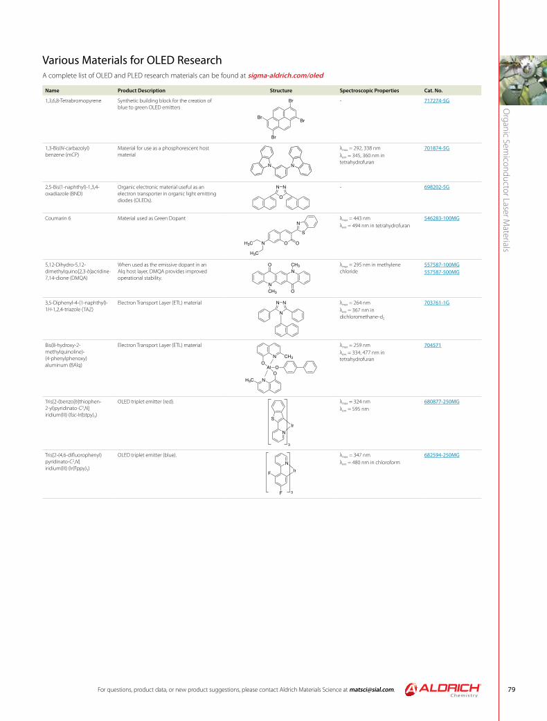
For questions, product data, or new product suggestions, please contact Aldrich Materials Science at [email protected]. 79
Organic Sem
iconductor Laser Materials
Various Materials for OLED ResearchA complete list of OLED and PLED research materials can be found at sigma-aldrich.com/oled
Name Product Description Structure Spectroscopic Properties Cat. No.
1,3,6,8-Tetrabromopyrene Synthetic building block for the creation of blue to green OLED emitters
Br
Br
Br
Br
- 717274-5G
1,3-Bis(N-carbazolyl)benzene (mCP)
Material for use as a phosphorescent host material
NN
λmax = 292, 338 nmλem = 345, 360 nm in tetrahydrofuran
701874-5G
2,5-Bis(1-naphthyl)-1,3,4-oxadiazole (BND)
Organic electronic material useful as an electron transporter in organic light emitting diodes (OLEDs).
NN
O
- 698202-5G
Coumarin 6 Material used as Green Dopant
O ONH3C
H3C
S
Nλmax = 443 nmλem = 494 nm in tetrahydrofuran
546283-100MG
5,12-Dihydro-5,12-dimethylquino[2,3-b]acridine-7,14-dione (DMQA)
When used as the emissive dopant in an Alq host layer, DMQA provides improved operational stability.
N
NO
OCH3
CH3 λmax = 295 nm in methylene chloride
557587-100MG557587-500MG
3,5-Diphenyl-4-(1-naphthyl)-1H-1,2,4-triazole (TAZ)
Electron Transport Layer (ETL) material NN
N
λmax = 264 nmλem = 367 nm in dichloromethane-d2
703761-1G
Bis(8-hydroxy-2-methylquinoline)-(4-phenylphenoxy)aluminum (BAlq)
Electron Transport Layer (ETL) material
N CH3
O
NO
H3C
Al O
λmax = 259 nmλem = 334, 477 nm in tetrahydrofuran
704571
Tris[2-(benzo[b]thiophen-2-yl)pyridinato-C3,N]iridium(III) (fac-Ir(btpy)3)
OLED triplet emitter (red).
S
N
Ir
3
λmax = 324 nmλem = 595 nm
680877-250MG
Tris[2-(4,6-difluorophenyl)pyridinato-C2,N]iridium(III) (Ir(Fppy)3)
OLED triplet emitter (blue).N
Ir
3F
F
λmax = 347 nmλem = 480 nm in chloroform
682594-250MG
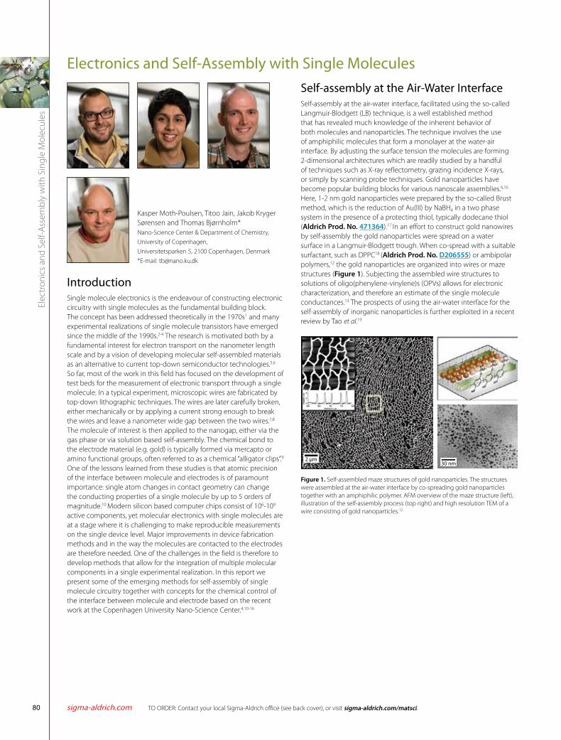
TO ORDER: Contact your local Sigma-Aldrich office (see back cover), or visit sigma-aldrich.com/matsci.sigma-aldrich.com80
Elec
tron
ics a
nd S
elf-A
ssem
bly
with
Sin
gle
Mol
ecul
es
Kasper Moth-Poulsen, Titoo Jain, Jakob Kryger Sørensen and Thomas Bjørnholm* Nano-Science Center & Department of Chemistry, University of Copenhagen, Universitetsparken 5, 2100 Copenhagen, Denmark *E-mail: [email protected]
IntroductionSingle molecule electronics is the endeavour of constructing electronic circuitry with single molecules as the fundamental building block. The concept has been addressed theoretically in the 1970s1 and many experimental realizations of single molecule transistors have emerged since the middle of the 1990s.2-4 The research is motivated both by a fundamental interest for electron transport on the nanometer length scale and by a vision of developing molecular self-assembled materials as an alternative to current top-down semiconductor technologies.5,6 So far, most of the work in this field has focused on the development of test beds for the measurement of electronic transport through a single molecule. In a typical experiment, microscopic wires are fabricated by top-down lithographic techniques. The wires are later carefully broken, either mechanically or by applying a current strong enough to break the wires and leave a nanometer wide gap between the two wires.7,8 The molecule of interest is then applied to the nanogap, either via the gas phase or via solution based self-assembly. The chemical bond to the electrode material (e.g. gold) is typically formed via mercapto or amino functional groups, often referred to as a chemical “alligator clips”.9 One of the lessons learned from these studies is that atomic precision of the interface between molecule and electrodes is of paramount importance: single atom changes in contact geometry can change the conducting properties of a single molecule by up to 5 orders of magnitude.10 Modern silicon based computer chips consist of 106-109 active components, yet molecular electronics with single molecules are at a stage where it is challenging to make reproducible measurements on the single device level. Major improvements in device fabrication methods and in the way the molecules are contacted to the electrodes are therefore needed. One of the challenges in the field is therefore to develop methods that allow for the integration of multiple molecular components in a single experimental realization. In this report we present some of the emerging methods for self-assembly of single molecule circuitry together with concepts for the chemical control of the interface between molecule and electrode based on the recent work at the Copenhagen University Nano-Science Center.4,10-16
Self-assembly at the Air-Water InterfaceSelf-assembly at the air-water interface, facilitated using the so-called Langmuir-Blodgett (LB) technique, is a well established method that has revealed much knowledge of the inherent behavior of both molecules and nanoparticles. The technique involves the use of amphiphilic molecules that form a monolayer at the water-air interface. By adjusting the surface tension the molecules are forming 2-dimensional architectures which are readily studied by a handful of techniques such as X-ray reflectometry, grazing incidence X-rays, or simply by scanning probe techniques. Gold nanoparticles have become popular building blocks for various nanoscale assemblies.6,16 Here, 1-2 nm gold nanoparticles were prepared by the so-called Brust method, which is the reduction of Au(III) by NaBH4 in a two phase system in the presence of a protecting thiol, typically dodecane thiol (Aldrich Prod. No. 471364).17 In an effort to construct gold nanowires by self-assembly the gold nanoparticles were spread on a water surface in a Langmuir-Blodgett trough. When co-spread with a suitable surfactant, such as DPPC18 (Aldrich Prod. No. D206555) or ambipolar polymers,12 the gold nanoparticles are organized into wires or maze structures (Figure 1). Subjecting the assembled wire structures to solutions of oligo(phenylene-vinylene)s (OPVs) allows for electronic characterization, and therefore an estimate of the single molecule conductances.13 The prospects of using the air-water interface for the self-assembly of inorganic nanoparticles is further exploited in a recent review by Tao et al.19
30 nm2 μm
Figure 1. Self-assembled maze structures of gold nanoparticles. The structures were assembled at the air-water interface by co-spreading gold nanoparticles together with an amphiphilic polymer. AFM overview of the maze structure (left), illustration of the self-assembly process (top right) and high resolution TEM of a wire consisting of gold nanoparticles.12
Electronics and Self-Assembly with Single Molecules
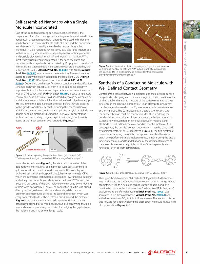
For questions, product data, or new product suggestions, please contact Aldrich Materials Science at [email protected]. 81
Electronics and Self-Assembly w
ith Single Molecules
Self-assembled Nanogaps with a Single Molecule IncorporatedOne of the important challenges in molecular electronics is the preparation of a 1-2 nm nanogap with a single molecule situated in the nanogap. In a recent report, gold nanorods were used to bridge the gap between the molecular length scale (1-2 nm) and the micrometer length scale, which is readily accessible by simple lithographic techniques.11 Gold nanorods have recently attracted large interest due to their ease of synthesis, unique shape dependant optical properties, and possible biochemical imaging20 and medical applications.21 The most widely used preparation method is the seed-mediated and surfactant assisted synthesis, first reported by Murphy and co-workers.22 In brief, citrate-stabilized gold nanoparticle seeds are prepared by the reduction of HAuCl4 (Aldrich Prod. No. 484385) with NaBH4 (Aldrich Prod. No. 480886) in an aqueous citrate solution. The seeds are then added to a growth solution containing the surfactant CTAB (Aldrich Prod. No. H9151), HAuCl4 and ascorbic acid (Aldrich Prod. No. A5960). Depending on the specific growth conditions and purification schemes, rods with aspect ratios from 4 to 25 can be prepared.23,24 Important factors for the successful synthesis are the use of the correct type of CTAB surfactant25 (Aldrich batch H6269), precise temperature control and clean glassware. Gold nanorod dimers can be prepared by addition of a water soluble thiol end-functionalized polyethylene glycol (HS-PEG-SH) to the gold nanoparticle seeds before they are exposed to the growth conditions. By carefully tuning the concentration of HS-PEG-SH the reaction conditions are optimized to yield a high degree of gold nanorod dimers. By diluting the HS-PEG-SH concentration further, one can, to a high degree, expect that a single molecule is acting as the linker between two nanorods (Figure 2).11
AuNPs Linked AuNPs
Linked Gold Nanorods
self-assembly growth
200 nm 5 nm
Figure 2. Scheme depicting the synthesis of linked gold nanords (left). TEM images of linked gold nanorods at different magnifications (right).11
In another experiment (Figure 3), the electronic properties of the gold rods were tested. First, gold nanorods were self-assembled to gold nanoparticle-coated tin oxide nanowires. The assembly was facilitated using thiol end-capped oligo(phenylenevinylene)s (OPVs) which are interesting test molecules exceeding low tunneling barriers26 and widely used in molecular electronic experiments.4,10 Second, the electronic properties of the OPV molecule were probed by conducting atomic force microscopy (C-AFM). The conductive AFM tip was placed directly on the gold nanorod as one electrode, while the much larger tin oxide nanowire acted as the second electrode, which was easily connected to close the electronic circuit around the molecule (Figure 3). I-V characteristics revealed signatures similar to those previously obtained for OPV molecules, thus also confirming that gold nanorods may be promising candidates for bridging the gap between the molecular and micrometer length scale.
Goldnanorod
500 nm
SnO2:Sb nanowire
Figure 3. Artistic impression of the measuring of a single or a few molecules via a conducting AFM tip (left) and AFM picture (right) of gold nanorods self-assembled to tin oxide nanowires mediated by thiol end-capped oligo(phenylenevinylene) molecules.14
Synthesis of a Conducting Molecule with Well Defined Contact GeometryControl of the contact between a molecule and the electrode surface has proved challenging since minute changes in atomic position of the binding thiol or the atomic structure of the surface may lead to large difference in the electronic properties.27 In an attempt to circumvent the challenges discussed above, C60 was introduced as an alternative anchoring group. The C60 molecule can create a strong contact to the surface through multiple connection sites, thus rendering the details of the contact site less important since the limiting tunneling barrier is now moved from the interface between molecule and electrode to well defined chemical bonds inside the molecule. As a consequence, the detailed contact geometry can then be controlled by chemical synthesis of C60 derivatives (Figure 4). The first electronic measurements taking use of this concept was described by Martin et al.15 who performed single molecule measurements using the break junction technique, and found that one of the dominant features of the molecule was extremely high stability of the single molecule junctions - even at room temperature.
NH
HN
OHO
OOH
N NH2CO
1,2-dichlorobenzenereflux
+2
Figure 4. Synthesis of a Würster’s blue derivative with C60 alligator clips.15
The C60-anchored molecule (1,4-bis(fullero[c]pyrrolidin-1-yl)benzene) was synthesized via [2+3]cycloaddition reaction of an in situ generated azomethine ylide to a fullerene carbon-carbon double bond. This reaction is known as the Prato-reaction.28 In brief, N,N’-(1,4-phenylene)bisglycine and paraformaldehyde (Aldrich Prod. No. 16005) was sonicated in 1,2-dicholorbenzene (Aldrich Prod. No. 240664) and added to a solution of C60 in 1,2-dichlorobenzene. The reaction mixture was refluxed for 6 hours yielding the black target molecule in 28% yield after purification (Figure 4).15
TO ORDER: Contact your local Sigma-Aldrich office (see back cover), or visit sigma-aldrich.com/matsci.sigma-aldrich.com82
Elec
tron
ics a
nd S
elf-A
ssem
bly
with
Sin
gle
Mol
ecul
es
ConclusionIn order to be able to study the intrinsic charge transport mechanisms in individual molecules, one of the main challenges is to circumvent problems associated with the specific position of the bonds between electrodes and molecules. A strategy for predefining the metal-molecule interface, and thereby achieving atomic scale precision, by the introduction of new C60-based anchoring groups have been presented. Another challenge is the fact that only one molecular junction is realized per device, hence the realization of molecular circuitry with numerous individual addressable components is highly desirable. Alternative routes that may help overcome these challenges are the use of chemical bottom-up fabrication techniques such as the Langmuir-Blodgett technique or other self-assembly based methods that may aid in the development towards complex circuitry. One possibility is the bottom-up synthesis of electrodes (gold nanorods) with molecules incorporated directly in the nanogap and prepared by the use of simple aqueous solution-based chemistries.
References:(1) Aviram, A; Ratner, M. A. Chem Phys. Lett. 1974, 29, 277-283. (2) Reed, M. A.; Zhou, C.; Muller, C. J.; Burgin, P.; Tour, J. M. Science 1997, 278,
252-254 (3) Joachim, C.; Gimzewski, J. K.; Schlittler, R. R.; Chavy, C. Phys. Rev. Lett., 1995, 74,
2102-2105. (4) Moth-Poulsen, K.; Bjørnholm, T. Nature Nanotech 2009, 4(9), 551-556. (5) Smits, E. S. G. et al. Nature, 2008, 455, 956-959. (6) Westerlund, F.; Bjørnholm, T. Curr. Opin. Colloid In. 2009, 14, 126-134. (7) Martin, C. A.; Ding, D.; van der Zant, H. S. J.; van Ruitenbeek, J. M. New J. Phys.
2008, 10, 065008. (8) Prokopuk, N.; Son, K-A. J. Phys.: Condens. Matter 2008, 20, 374116. (9) Pearson, D. L.; Tour, J. M. J. Org. Chem. 1997, 62 (5), 1376-1387.
(10) Danilov, A.; Kubatkin, S.; Kafanov, S.; Hedegard, P.; Stuhr-Hansen, N.; Moth-Poulsen, K; Bjørnholm, T. Nano Letters 2008, 8 (1) 1-5.
(11) Jain, T.; Westerlund, F.; Johnson, E.; Moth-Poulsen, K.; Bjørnholm, T. ACS Nano. 2009, 3 (4), 828-834
(12) Hansen, C.; Westerlund, F.; Moth-Poulsen, K.; Ravindranath, R.; Valiyaveettil, S.; Bjørnholm, T. Langmuir 2008, 24, 3905-3910.
(13) Hassenkam, T.; Moth-Poulsen, K.; Stuhr-Hansen, N.; Nørgaard, K.; Kabir, M. S.; Bjørnholm, T. Nano Letters 2004, 4 (1).
(14) Tang, Q.; Tong, Y.; Jain, T.; Hassenkam, T.; Wan, Q.; Moth-Poulsen, K.; Bjørnholm, T. Nanotechnology 2009, 20 (24), 245205
(15) Martin, C. A.; Ding, D.; Sørensen, J. K.; Bjørnholm, T.; van Ruitenbeek, J. M.; van der Zant, H. S. J. J. Am. Chem. Soc. 2008, 130, 13198-13199.
(16) Nørgaard, K.; Bjørnholm, T. Chem. Commun. 2005, 1812. (17) Brust, M.; Walker, M.; Bethell, D.; Schiffrin, D. J.; Whyman, R. J. Chem. Soc., Chem.
Commun. 1994, 801. (18) Hassenkam, T.; Nørgaard, K.; Iversen, L.; Kiely, C. J.; Brust, M.; Bjørnholm, T. Adv.
Mater. 2002, 14, 1126. (19) Tao, A. R.; Huang, J. X.; Yang, P. D. Acc. Chem. Res. 2008, 41 (12) 1662-1673. (20) Murphy, C. J.; Gole, A. M.; Hunyadi, S. E.; Stone, J. W.; Sisco, P. N.; Alkilany, A.,
Chem. Commun. 2008, 5, 544–557. (21) Huang, X.; Jain, P. K.; El-Sayed, I. H.; El-Sayed, M. A. Lasers Med. Sci. 2008, 23,
217–228. (22) Jana, N. R.; Gearheart, L.; Murphy, C. J. Adv. Mater. 2001, 13, 1389–1393. (23) Gao, J.; Bender, C. M.; Murphy, C. J. Langmuir 2003, 19, 9065–9070. 10 (24) Grzelczak, M.; Perez-Juste, J.; Mulvaney, P.; Liz-Marzan, L. M. Chem. Soc. Rev.
2008, 37, 1783–1791. (25) Smith, D. K.; Korgel, B. A. Langmuir 2008, 24, 644-649 (26) Moth-Poulsen, K.; Patrone, L.; Stuhr-Hansen, N.; Christensen, J. B.; Bourgoin
J.-P.; Bjørnholm, T. Nano Lett. 2005, 5 (4): 783-785. (27) (a) Moore, A. M.; Dameron, A. A.; Mantooth, B. A.; Smith, R. K.; Fuchs, D. J.;
Ciszek, J. W.; Maya, F.; Yao, Y.; Tour, J. M.; Weiss, P. S. J. Am. Chem. Soc. 2006, 128, 1959–1967. (b) Ulrich, J.; Esrail, D.; Pontius, W.; Venkataraman, L.; Millar, D.; Doerrer, L. H. J. Phys. Chem. B 2006, 110, 2462–2466. (c) Li, C.; Pobelov, I.; Wandlowski, T.; Bagrets, A.; Arnold, A.; Evers, F. J. Am. Chem. Soc. 2008, 130, 318–326.
(28) Maggini, M.; Scorrano, G.; Prato, M. J. Am. Chem. Soc. 1993, 115, 9798–9799
Self-Assembly MaterialsA comprehensive library of self-assembly materials can be viewed at sigma-aldrich.com/self-assembly
Monofunctional ThiolsName Chain Length Structure Purity/Concentration Cat. No.
Cyclohexanethiol
n HS
97% C105600-25GC105600-100G
m-Carborane-9-thiol
nHS
97% 686506-250MG
m-Carborane-1-thiol
n HS
96% 695572-250MG
1-Adamantanethiol
n HS
95% 659452-5G
NanoThinks™ 8 n HS5 mM in ethanol 662208-100ML
1-Decanethiol n HS99% 705233-1G
1,1’,4’,1’’-Terphenyl-4-thiol n HS
97% 708488-500MG
1-Dodecanethiol
n HS
≥98% 471364-100ML471364-500ML471364-2L471364-18L
Chain Length Key: n 0–5 n 6–10 n 11–15 n 16+
For questions, product data, or new product suggestions, please contact Aldrich Materials Science at [email protected]. 83
Electronics and Self-Assembly w
ith Single Molecules
Name Chain Length Structure Purity/Concentration Cat. No.
1-Hexadecanethiol n HS99% 674516-500MG
NanoThinks™ 18 n HS5 mM in ethanol 662194-100ML
(11-Mercaptoundecyl)tri(ethyleneglycol)monomethyl ether
n HS O
OMe
3
≥95% 717002-250MG
(11-Mercaptoundecyl)hexa(ethylene glycol)monomethyl ether
n HS O
OMe
6
≥95% 716995-250MG
Bifunctional MoleculesName Chain Length Structure Purity/Concentration Cat. No.
3-Mercaptopropionic acid n HS
COOH≥99% M5801-5G
M5801-100GM5801-500G
3-Mercapto-1-propanoln HS OH
95% 405736-1G405736-5G
1,4-Butanedithioln HS
SH 97% B85404-5GB85404-25G
4-Cyano-1-butanethiol n HS CN97% 692581-500MG
1,6-Hexanedithioln HS
SH 96% H12005-5GH12005-25G
8-Mercaptooctanoic acid n COOHHS
95% 675075-1G
NanoThinks™ THIO8n HS
SH 5 mM in ethanol 662615-100ML
8-Mercapto-1-octanoln HS
OH 98% 706922-1G
2,2’-(Ethylenedioxy)diethanethiol n HS
O
O
SH 95% 465178-100ML465178-500ML
4,4’-Dimercaptostilbene
nHS
SH
>96% 701696-100MG
6-(Ferrocenyl)hexane-thiol
n
HS
Fe
- 682527-250MG
11-Bromo-1-undecanethiol n HS Br
99% 701335-250MG
11-Amino-1-undecanethiol hydrochloride
n HS NH2 HCl.99% 674397-50MG
11-Mercapto-1-undecanol n HS OH
99% 674249-250MG
12-Mercapto- dodecanoic acid n HS COOH
99% 705241-500MG
p-Terphenyl-4,4’’-dithiol
n SHHS
96% 704709-1G
NanoThinks™ ACID16 n COOHHS5 mM in ethanol 662216-100ML
Triethylene glycol mono-11-mercaptoundecyl ether
n HS O
OH
3
95% 673110-250MG
(11-Mercaptoundecyl)tetra(ethylene glycol) n HS O
OH
4
95% 674508-250MG
(11-Mercaptoundecyl)hexa(ethylene glycol) n HS O
OH
6
95% 675105-250MG
Chain Length Key: n 0–5 n 6–10 n 11–15 n 16+
TO ORDER: Contact your local Sigma-Aldrich office (see back cover), or visit sigma-aldrich.com/matsci.sigma-aldrich.com84
Elec
tron
ics a
nd S
elf-A
ssem
bly
with
Sin
gle
Mol
ecul
es
Protected Thiols for In-situ DeprotectionName Chain Length Structure Purity Cat. No.
S-(4-Cyanobutyl)thioacetate n
H3C S
O
CN
97% 694754-1G
1,4-Butanedithiol diacetate
n H3C S
S CH3
O
O
97% 558826-1G558826-5G
S-(11-Bromoundecyl)thioacetate n
H3C S Br
O 95% 706930-1G
S-[4-[2-[4-(2-Phenyl-ethynyl)phenyl]ethynyl]phenyl] thioacetate n
H3C S
O ≥95% 718378-100MG
S,S’-[1,4-Phenylenebis(2,1-ethynediyl-4,1- phenylene)]bis(thioacetate)
nH3C S
O
S CH3
O ≥95% 718351-100MG
[11-(Methyl- carbonylthio)undecyl]tetra(ethylene glycol) n
H3C S O
OH
O
4
95% 674176-250MG
Hexa(ethylene glycol)mono-11-(acetylthio)undecyl ether n
H3C S
O
O
OH
6
95% 675849-250MG
Chain Length Key: n 0–5 n 6–10 n 11–15 n 16+
Gold NanostructuresNanoparticles
Name Physical Form Particle Size (nm) Cat. No.
Gold nanopowder, HAuCl4 particle size <100 636347-1G
Gold colloid dispersionnanoparticles, ~ 0.01%~ 1 A520 units/mL
mean particle size 17 - 23 (monodisperse)particle size 20
G1652-25ML
dispersionnanoparticles, ~ 0.01%~ 1 A520 units/mL
mean particle size 8.5 - 12.0 (monodisperse)particle size 10
G1527-25ML
dispersionnanoparticles, ~ 0.01%~ 1 A520 units/mL
mean particle size 3.0 - 5.5 (monodisperse)particle size 5
G1402-25ML
Octanethiol functionalized gold nanoparticles solution, 2 % (w/v) in toluene particle size 2 - 4 DLS) 660426-5ML
Dodecanethiol functionalized gold nanoparticles solution, 2 % (w/v) in toluene particle size 3 - 5 TEM) 660434-5ML
dispersion, 0.01% in toluene particle size 3 - 6 54349-10ML-F
Bare NanorodsName Absorption Physical Form Diam. × L (nm) Cat. No.
Gold nanorods 780 nm dispersion, 35 μg/mL in H2O 10 × 38 716812-25ML
808 nm dispersion, 36 μg/mL in H2O 10 × 41 716820-25ML
850 nm dispersion, 35 μg/mL in H2O 10 × 45 716839-25ML
550 nm dispersion, 171 μg/mL in H2O 25 × 34 716847-25ML
600 nm dispersion, 235 μg/mL in H2O 25 × 44 716855-25ML
650 nm dispersion, 150 μg/mL in H2O 25 × 60 716863-25ML
Gold microrods - dispersion, 50 μg/mL in H2O 200 × 1000 716960-10ML

For questions, product data, or new product suggestions, please contact Aldrich Materials Science at [email protected]. 85
Electronics and Self-Assembly w
ith Single Molecules
Functionalized NanorodsName Absorption Physical Form Diam. × L (nm) Cat. No.
Gold nanorods, amine terminated 808 nm dispersion, 0.9 mg/mL in H2O 10 × 41 716871-1ML
Gold nanorods, carboxyl terminated 808 nm dispersion, 0.9 mg/mL in H2O 10 × 41 716898-1ML
Gold nanorods, methyl terminated 808 nm dispersion, 0.9 mg/mL in H2O 10 × 41 716901-1ML
Catalytic NanorodsName Absorption Physical Form Diam. × L (nm) Cat. No.
Gold nanorods, palladium coated 700 nm dispersion, 100 μg/mL in H2O 25 × 75 716928-10ML
Gold nanorods, platinum coated 700 nm dispersion, 100 μg/mL in H2O 25 × 75 716936-10ML
NanowiresName Physical Form Diam. × L (nm) Cat. No.
Gold nanowires dispersion, 0.6 mg/mL in H2O 30 × 4,500 716944-10ML
dispersion, 0.5 mg/mL in H2O 30 × 6,000 716952-10ML
Gold Nanoparticle PrecursorsChemical Structure Name Cat. No.
AuCl3 Gold(III) chloride, ≥99.99% trace metals basis 379948-250MG379948-1G
HAuCl4 Gold(III) chloride, 99.99% trace metals basis 484385-10G484385-50G
HAuCl4 · xH2O Gold(III) chloride, 99.999% trace metals basis 254169-500MG254169-5G
HAuCl4 · 3H2O Gold(III) chloride, ≥99.9% trace metals basis 520918-1G520918-5G520918-25G
AuCl4K Potassium gold(III) chloride, 99.995% trace metals basis 450235-250MG450235-1G
sigma-aldrich.com
Material Matters™
A Quarterly Periodical from Aldrich Materials Science
Hot topics in high-tech materials research
Theme-based technical reviews by leading experts
Constructive application notes
New product highlights and services
Receive your free subscription to Material Matters™: sigma-aldrich.com/mm
Aldrich Materials Science – We focus on materials so you can focus on results
LSU72175-508473
0109
World Headquarters3050 Spruce St., St. Louis, MO 63103(314) 771-5765sigma-aldrich.com
Order/Customer Service (800) 325-3010 • Fax (800) 325-5052
Technical Service (800) 325-5832 • sigma-aldrich.com/techservice
Development/Custom Manufacturing Inquiries (800) 244-1173
Safety-related Information sigma-aldrich.com/safetycenter
©2009 Sigma-Aldrich Co. All rights reserved. SIGMA, , SAFC, , SIGMA-ALDRICH, ALDRICH, , FLUKA, , and SUPELCO, are trademarks belonging to Sigma-Aldrich Co. and its affiliate Sigma-Aldrich Biotechnology, L.P. Sigma brand products are sold through Sigma-Aldrich, Inc. Sigma-Aldrich, Inc. warrants that its products conform to the information contained in this and other Sigma-Aldrich publications. Purchaser must determine the suitability of the product(s) for their particular use. Additional terms and conditions may apply. Please see reverse side of the invoice or packing slip. Eppendorf is a registered trademark of Eppendorf-Netheler-Hinz GmbH. Sepharose is a registered trademark of GE Healthcare. IGEPAL is a registered trademark of General Dyestuff Corp. Coomassie is a registered trademark of Imperial Chemical Industries Ltd. Plexcore is a registered trademark of Plextronics, Inc. NanoThinks and ProteoSilver are trademarks of Sigma-Aldrich Biotechnology LP and Sigma-Aldrich Co. Boramer is a trademark of TDA Research, Inc.
Sigma-Aldrich3050 Spruce StreetSt. Louis, MO 63103 USAsigma-aldrich.com
Accelerating Customers’ Success through Innovation and
Leadership in Life Science, High Technology and Service
ArgentinaSIGMA-ALDRICH DE ARGENTINA S.A. Free Tel: 0810 888 7446 Tel: (+54) 11 4556 1472 Fax: (+54) 11 4552 1698
AustraliaSIGMA-ALDRICH PTY LTD. Free Tel: 1800 800 097 Free Fax: 1800 800 096 Tel: (+61) 2 9841 0555 Fax: (+61) 2 9841 0500
AustriaSIGMA-ALDRICH HANDELS GmbH Tel: (+43) 1 605 81 10 Fax: (+43) 1 605 81 20
BelgiumSIGMA-ALDRICH NV/S.A.Free Tel: 0800 14747 Free Fax: 0800 14745 Tel: (+32) 3 899 13 01 Fax: (+32) 3 899 13 11
BrazilSIGMA-ALDRICH BRASIL LTDA.Free Tel: 0800 701 7425 Tel: (+55) 11 3732 3100 Fax: (+55) 11 5522 9895
CanadaSIGMA-ALDRICH CANADA LTD.Free Tel: 1800 565 1400 Free Fax: 1800 265 3858 Tel: (+1) 905 829 9500 Fax: (+1) 905 829 9292
ChileSIGMA-ALDRICH QUIMICA LIMITADATel: (+56) 2 495 7395 Fax: (+56) 2 495 7396
ChinaSIGMA-ALDRICH (SHANGHAI) TRADING CO. LTD.Free Tel: 800 819 3336 Tel: (+86) 21 6141 5566 Fax: (+86) 21 6141 5567
Czech RepublicSIGMA-ALDRICH spol. s r. o. Tel: (+420) 246 003 200 Fax: (+420) 246 003 291
DenmarkSIGMA-ALDRICH DENMARK A/S Tel: (+45) 43 56 59 00 Fax: (+45) 43 56 59 05
FinlandSIGMA-ALDRICH FINLAND OYTel: (+358) 9 350 9250 Fax: (+358) 9 350 92555
FranceSIGMA-ALDRICH CHIMIE S.à.r.l. Free Tel: 0800 211 408Free Fax: 0800 031 052Tel: (+33) 474 82 28 00 Fax: (+33) 474 95 68 08
GermanySIGMA-ALDRICH CHEMIE GmbHFree Tel: 0800 51 55 000 Free Fax: 0800 64 90 000 Tel: (+49) 89 6513 0 Fax: (+49) 89 6513 1160
GreeceSIGMA-ALDRICH (O.M.) LTD.Tel: (+30) 210 994 8010 Fax: (+30) 210 994 3831
HungarySIGMA-ALDRICH Kft Ingyenes telefonszám: 06 80 355 355 Ingyenes fax szám: 06 80 344 344 Tel: (+36) 1 235 9055 Fax: (+36) 1 235 9050
IndiaSIGMA-ALDRICH CHEMICALS PRIVATE LIMITED Telephone Bangalore: (+91) 80 6621 9400 New Delhi: (+91) 11 4358 8000 Mumbai: (+91) 22 2570 2364 Hyderabad: (+91) 40 4015 5488Kolkata: (+91) 33 4013 8003 Fax Bangalore: (+91) 80 6621 9650 New Delhi: (+91) 11 4358 8001 Mumbai: (+91) 22 2579 7589 Hyderabad: (+91) 40 4015 5466Kolkata: (+91) 33 4013 8016
IrelandSIGMA-ALDRICH IRELAND LTD. Free Tel: 1800 200 888 Free Fax: 1800 600 222Tel: (+353) 402 20370Fax: (+ 353) 402 20375
IsraelSIGMA-ALDRICH ISRAEL LTD. Free Tel: 1 800 70 2222 Tel: (+972) 8 948 4100 Fax: (+972) 8 948 4200
ItalySIGMA-ALDRICH S.r.l. Numero Verde: 800 827018 Tel: (+39) 02 3341 7310 Fax: (+39) 02 3801 0737
JapanSIGMA-ALDRICH JAPAN K.K. Tel: (+81) 3 5796 7300 Fax: (+81) 3 5796 7315
KoreaSIGMA-ALDRICH KOREA Free Tel: (+82) 80 023 7111 Free Fax: (+82) 80 023 8111 Tel: (+82) 31 329 9000 Fax: (+82) 31 329 9090
MalaysiaSIGMA-ALDRICH (M) SDN. BHDTel: (+60) 3 5635 3321 Fax: (+60) 3 5635 4116
MexicoSIGMA-ALDRICH QUÍMICA, S.A. de C.V.Free Tel: 01 800 007 5300 Free Fax: 01 800 712 9920 Tel: (+52) 722 276 1600 Fax: (+52) 722 276 1601
The NetherlandsSIGMA-ALDRICH CHEMIE BVFree Tel: 0800 022 9088 Free Fax: 0800 022 9089 Tel: (+31) 78 620 5411 Fax: (+31) 78 620 5421
New ZealandSIGMA-ALDRICH NEW ZEALAND LTD. Free Tel: 0800 936 666 Free Fax: 0800 937 777 Tel: (+61) 2 9841 0555 Fax: (+61) 2 9841 0500
NorwaySIGMA-ALDRICH NORWAY AS Tel: (+47) 23 17 60 00 Fax: (+47) 23 17 60 10
PolandSIGMA-ALDRICH Sp. z o.o. Tel: (+48) 61 829 01 00 Fax: (+48) 61 829 01 20
PortugalSIGMA-ALDRICH QUÍMICA, S.A.Free Tel: 800 202 180 Free Fax: 800 202 178 Tel: (+351) 21 924 2555 Fax: (+351) 21 924 2610
RussiaSIGMA-ALDRICH RUS, LLC Tel: (+7) 495 621 5579 Fax: (+7) 495 621 5923
SingaporeSIGMA-ALDRICH PTE. LTD.Tel: (+65) 6779 1200 Fax: (+65) 6779 1822
SlovakiaSIGMA-ALDRICH spol. s r. o. Tel: (+421) 255 571 562Fax: (+421) 255 571 564
South AfricaSIGMA-ALDRICH (PTY) LTD.Free Tel: 0800 1100 75 Free Fax: 0800 1100 79 Tel: (+27) 11 979 1188 Fax: (+27) 11 979 1119
SpainSIGMA-ALDRICH QUÍMICA, S.A. Free Tel: 900 101 376 Free Fax: 900 102 028 Tel: (+34) 91 661 99 77 Fax: (+34) 91 661 96 42
SwedenSIGMA-ALDRICH SWEDEN ABTel: (+46) 8 742 4200 Fax: (+46) 8 742 4243
SwitzerlandSIGMA-ALDRICH CHEMIE GmbH Free Tel: 0800 80 00 80 Free Fax: 0800 80 00 81 Tel: (+41) 81 755 2828 Fax: (+41) 81 755 2815
United KingdomSIGMA-ALDRICH COMPANY LTD.Free Tel: 0800 717 181 Free Fax: 0800 378 785 Tel: (+44) 1747 833 000 Fax: (+44) 1747 833 313
United StatesSIGMA-ALDRICH Toll-Free: 800 325 3010 Toll-Free Fax: 800 325 5052 Tel: (+1) 314 771 5765 Fax: (+1) 314 771 5757
VietnamSIGMA-ALDRICH PTE LTD. VN R.O.Tel: (+84) 3516 2810 Fax: (+84) 6258 4238
Internet sigma-aldrich.com