Embed Size (px)
Citation preview
Ordering number: EP35E

Combining Power and Control, Sanyo Inverter Power IC Enables Easy Realization of Power Saving for Equipment
CONTENTS
To what extent can electrical equipment become environ-mentally friendly? One of the answers is power-saving and low-consumption power technology. Inverter technology realizes fine control of the revolving speed and power sav-ing for motors widely used for applications ranging from consumer appliances such as air conditioners, refrigera-tors, and washing machines, to FA equipment, robots, and other industrial equipment. The use of this technology requires solving of a number of issues such as complica-tion in circuit configuration, increases in mounting space and noise. Sanyo's inverter power ICs use an original insulated metal substrate technology (IMST) that mounts on an aluminum substrate power output elements such as IGBTs, MOSFETs, and bipolar transistors, ICs required for control, as well as passive devices with high-density mounting. Since all kinds of peripheral circuits such as protective circuits are also incorporated, solving the issues mentioned above, more compact design and higher reliability can also be achieved. From small power applications (3A) to large power applica-tions (50A), Sanyo's lineup of inverter power ICs, whose product grade has been further enhanced, realizes labor saving for system design together with power saving.
n Proposal for inverter control systems …………………………
n Three main technologies supporting Sanyo's inverter power ICs ……
n Development history …………………………………………
n Inverter circuit block diagram ………………………………
3
4
5
5
n Series lineup …………………………………………………
n IMST hybrid IC fabrication process …………………………
n Sample Sanyo inverter power IC products ………………
n Features of Sanyo inverter power ICs …………………
6
7
8--9
10--12
Energy Saving and high performance through inverter control
Washing machine
Air conditioner
Refrigerators
Washing machine
Air conditioner
Refrigerators

n Main specifications
•STK621-000 / STK611-000 Series ……………………
•STK650-000 / STK651-000 Series …………………………
•Active filter circuit characteristics improvement examples …
13--14
15
16
•STK762-000G Series ……………………………………
•STK623-000 Series ………………………………………
•STK630-000 Series ………………………………………
n Packages dimensions …………………………………
17
18
19
20--22
Cars
General-purpose inverter
NC machine tool
FA
Robots
Cars
General-purpose inverter
NC machine tool
FA
Robots
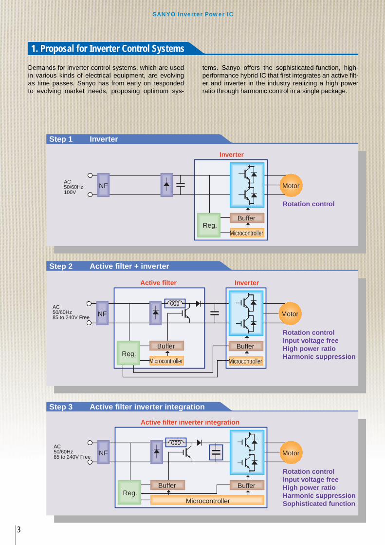
1. Proposal for Inverter Control Systems
SANYO Inverter Power IC
3
Demands for inverter control systems, which are used in various kinds of electrical equipment, are evolving as time passes. Sanyo has from early on responded to evolving market needs, proposing optimum sys-
tems. Sanyo offers the sophisticated-function, high-performance hybrid IC that first integrates an active filt-er and inverter in the industry realizing a high power ratio through harmonic control in a single package.
Inverter Step 1
Active filter + inverterStep 2
Active filter inverter integrationStep 3
Buffer
Motor
Reg.
NF
Microcontroller
Inverter
AC 50/60Hz100V
Rotation control
AC 50/60Hz85 to 240V Free
InverterActive filter
Buffer
MotorNF
Microcontroller
BufferReg.
Microcontroller
AC 50/60Hz85 to 240V Free
Active filter inverter integration
Buffer
MotorNF
Microcontroller
BufferReg.
Rotation control Input voltage free High power ratio Harmonic suppression
Rotation control Input voltage free High power ratio Harmonic suppression Sophisticated function
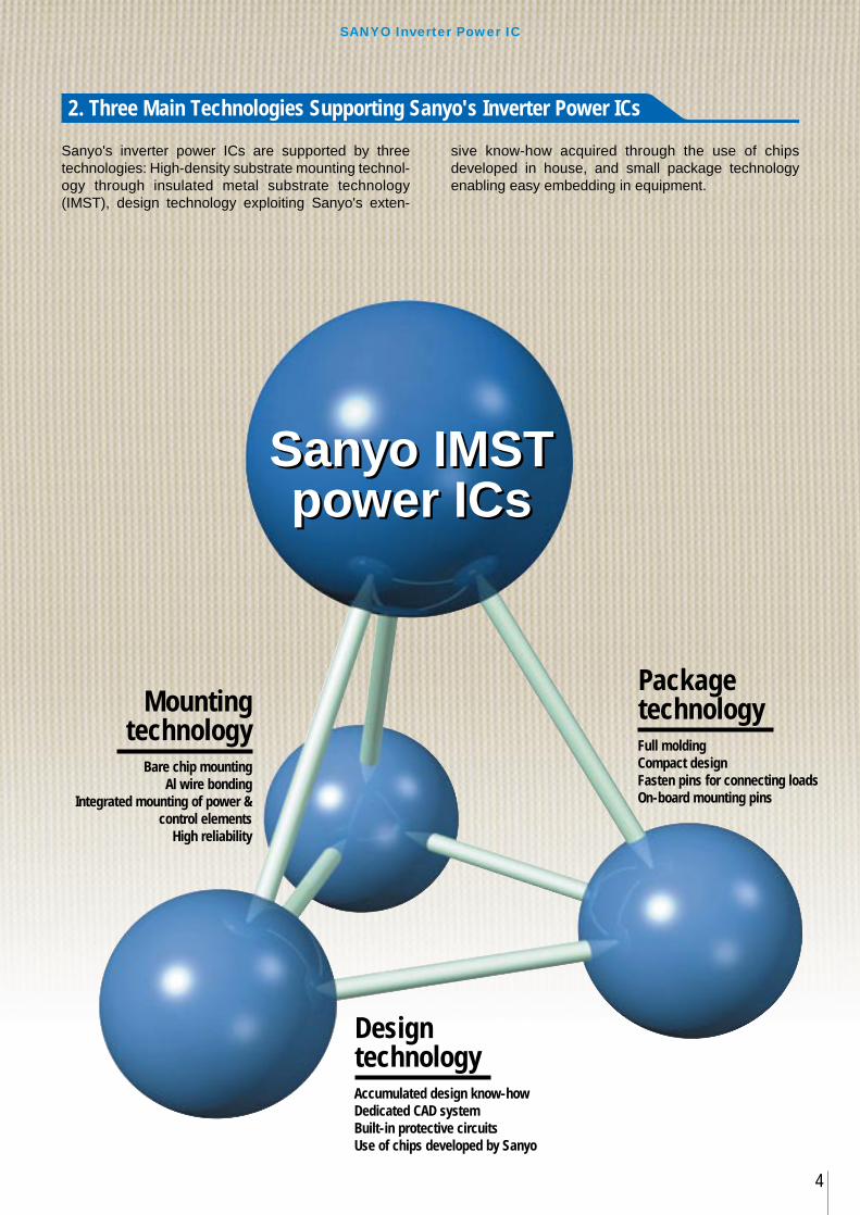
2. Three Main Technologies Supporting Sanyo's Inverter Power ICs
SANYO Inverter Power IC
4
Sanyo's inverter power ICs are supported by three technologies: High-density substrate mounting technol-ogy through insulated metal substrate technology (IMST), design technology exploiting Sanyo's exten-
sive know-how acquired through the use of chips developed in house, and small package technology enabling easy embedding in equipment.
Sanyo IMST power ICs
Mountingtechnology
Sanyo IMST power ICs
Bare chip mountingAl wire bonding
Integrated mounting of power &control elements
High reliability
PackagetechnologyFull molding Compact design Fasten pins for connecting loadsOn-board mounting pins
Designtechnology Accumulated design know-how Dedicated CAD system Built-in protective circuits Use of chips developed by Sanyo

SANYO Inverter Power IC
5
3. Development History
4. Block Diagram of Inverter Circuit
Sanyo developed and commercialized the inverter power IC STK65000 series in 1986, first proposing the "intelligent power module" concept in the industry, and
in 1989, successfully released the active filter power IC STK76000 Series.
1985 1990 1995 2000
STK65000MK2
STK65000MK3
STK762-000
STK76000
STK650-000 BJT
STK651-000 SIT
STK620-000 IGBT & 4 power supplies
STK621-000 IGBT & single power supply
STK621-010
STK611-000
Industry's
first
Industry's
first
Industry's
first
For PAM control
Small full molding package
Single control circuit power supply
ActivActive filter power IC
Inverter power IC er IC Inverter power IC
Active filter power IC
MotorNF
High-voltage interface block
Waveform generation / control block (CPU) Position detectionSpeed detection
Control power supply
Pre-drive power supply
Protective circuit block • Excessive temperature • Overvoltage • Overcurrent
Protective circuit block • Excessive temperature • Excessive saturation voltage • Overcurrent • Low supply voltage
Shunt resistor
Three-phase power drive block (for example IGBT)
Temperature detection
Temperature detection
Pre
-driv
e bl
ock
(6 c
ircui
ts)
Cont
rol/
pre-
drive
blo
ck
A
B
C
B+C
Inverter STK650-000 Series/STK651-000 Series
Inverter + high-voltage interface STK611-000 Series/STK621-000 Series
Active Filter STK762-000G Series
Inverter + Active Filter STK623-000 Series
Block Function Series Name
SANYO Inverter Power IC
6
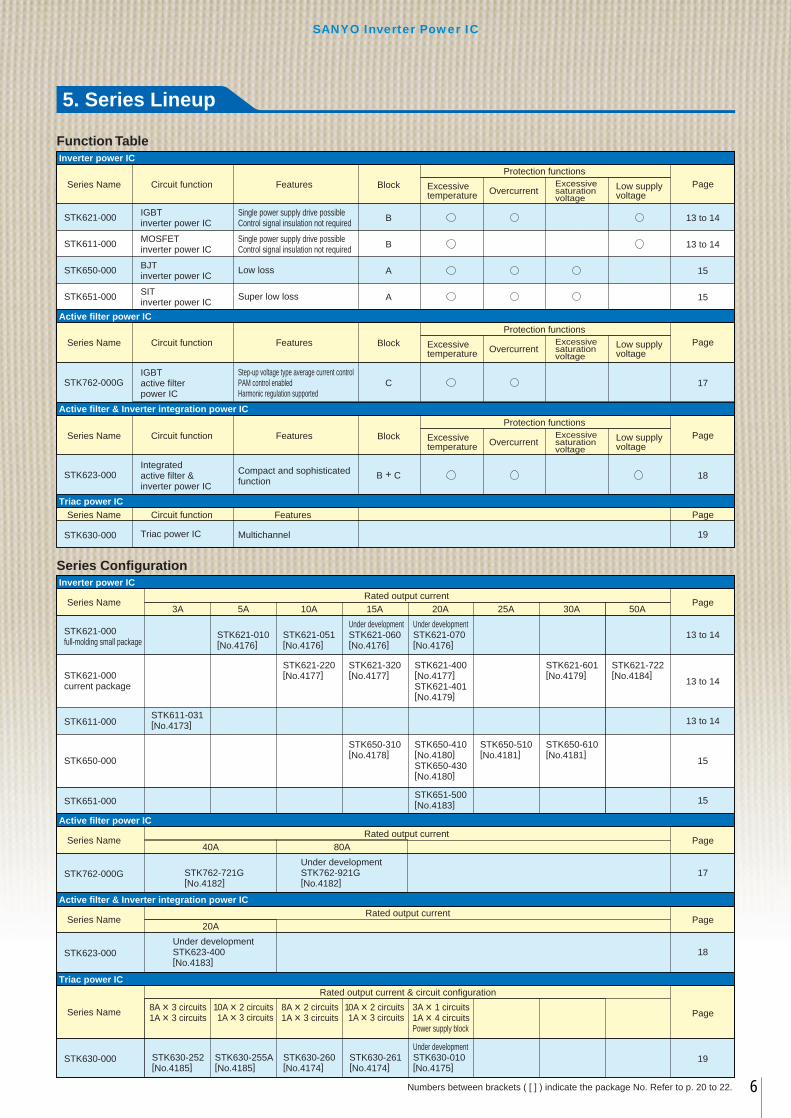
5. Series Lineup
Function TableInverter power IC
Series Name Circuit function Features Block
Protection functions
Excessivetemperature Overcurrent
Excessive saturation voltage
Low supply voltage
Page
STK621-000 IGBT inverter power IC
Single power supply drive possible Control signal insulation not required B 13 to 14
Active filter power IC
STK762-000GIGBT active filter power IC
Step-up voltage type average current controlPAM control enabled Harmonic regulation supported
C 17
Active filter & Inverter integration power IC
STK623-000Integrated active filter & inverter power IC
Compact and sophisticatedfunction
B + C 18
Triac power IC Series Name Circuit function Features
STK630-000 19Triac power IC Multichannel
STK611-000 MOSFET inverter power IC
Single power supply drive possible Control signal insulation not required B 13 to 14
STK650-000 BJT inverter power IC
Low loss A 15
STK651-000 SIT inverter power IC
Super low loss A 15
Series ConfigurationInverter power IC
Series Name3A 5A 10A 15A 20A 25A 30A 50A
Rated output current
STK621-000 full-molding small package
STK621-010[No.4176]
STK621-051[No.4176]
Under developmentSTK621-060[No.4176]
Under developmentSTK621-070[No.4176]
13 to 14
13 to 14
15
17
18
19
Active filter power IC
Series Name40A 80A
Rated output current
STK762-000GUnder developmentSTK762-921G[No.4182]
STK630-252[No.4185]
STK630-255A[No.4185]
STK630-260[No.4174]
STK630-261[No.4174]
Under developmentSTK630-010[No.4175]
STK762-721G[No.4182]
Active filter & Inverter integration power IC
Series Name20A
Rated output current
STK623-000Under developmentSTK623-400[No.4183]
Triac power IC
Series Name
Rated output current & circuit configuration
Page
STK630-000
Numbers between brackets ( [ ] ) indicate the package No. Refer to p. 20 to 22.
8A x 3 circuits1A x 3 circuits
10A x 2 circuits 8A x 2 circuits1A x 3 circuits
10A x 2 circuits1A x 3 circuits1A x 3 circuits
3A x 1 circuits1A x 4 circuitsPower supply block
STK651-000STK651-500[No.4183]
STK621-000 current package
STK621-220[No.4177]
STK621-320[No.4177]
STK621-400[No.4177]STK621-401[No.4179]
STK621-601[No.4179]
STK621-722[No.4184]
STK650-000
STK650-310[No.4178]
STK650-410[No.4180]STK650-430[No.4180]
STK650-510[No.4181]
STK650-610[No.4181]
STK611-000STK611-031[No.4173]
Page
Page
Page
Page
Series Name Circuit function Features Block
Protection functions
Protection functions
Excessivetemperature Overcurrent
Excessive saturation voltage
Low supply voltage
Page
Series Name Circuit function Features Block Excessivetemperature Overcurrent
Excessive saturation voltage
Low supply voltage
Page
13 to 14
15
SANYO Inverter Power IC
7
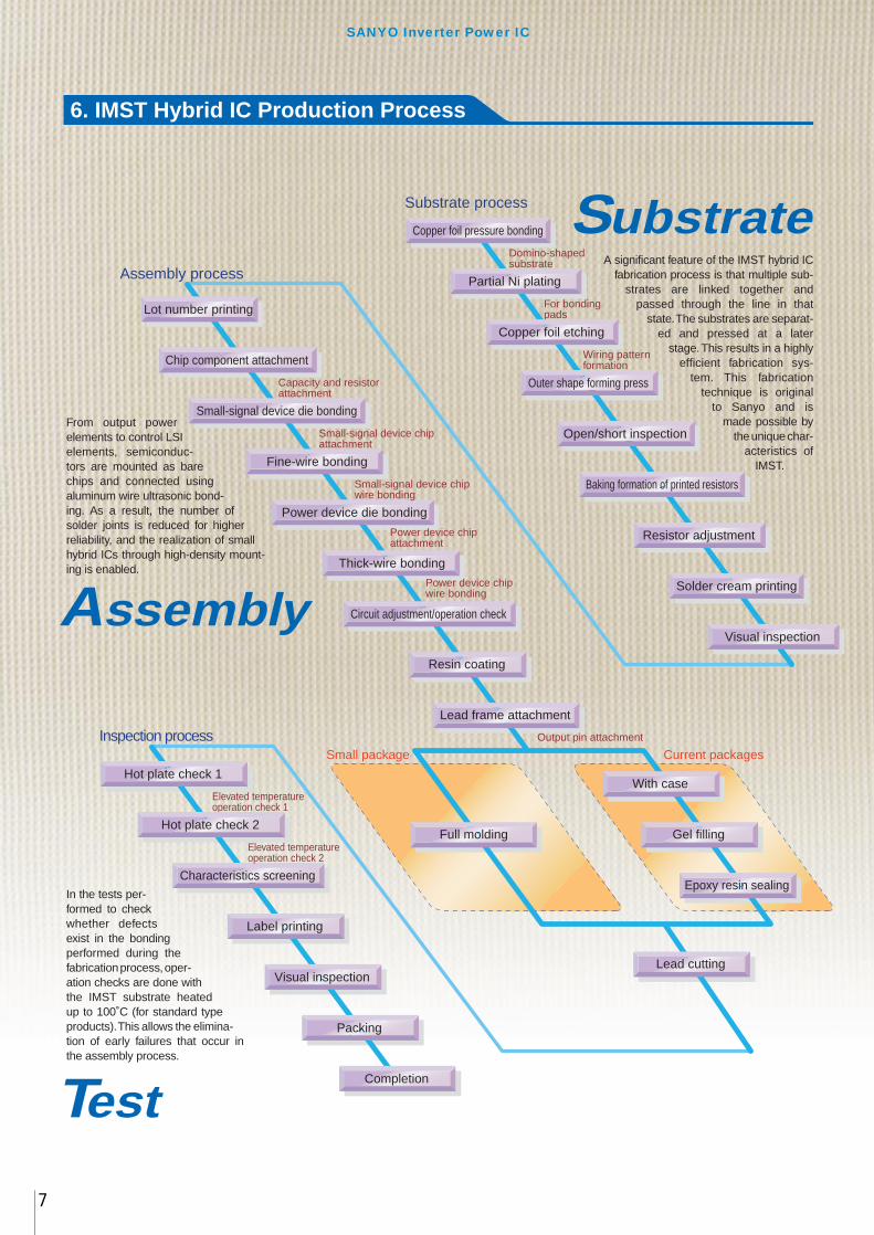
6. IMST Hybrid IC Production Process
From output power elements to control LSI elements, semiconduc-tors are mounted as bare chips and connected using aluminum wire ultrasonic bond-ing. As a result, the number of solder joints is reduced for higher reliability, and the realization of small hybrid ICs through high-density mount-ing is enabled.
In the tests per-formed to check whether defects exist in the bonding performed during the fabrication process, oper-ation checks are done with the IMST substrate heated up to 100˚C (for standard type products). This allows the elimina-tion of early failures that occur in the assembly process.
A significant feature of the IMST hybrid IC fabrication process is that multiple sub-
strates are linked together and passed through the line in that
state. The substrates are separat-ed and pressed at a later
stage. This results in a highly efficient fabrication sys-
tem. This fabrication technique is original
to Sanyo and is made possible by
the unique char-acteristics of
IMST.
Circuit adjustment/operation check
Resin coating
Chip component attachment
Small-signal device die bonding
Power device die bonding
Thick-wire bonding
Fine-wire bonding
Lead frame attachment
Lead cutting
Small package Current packages
Substrate process
Assembly process
Inspection process
Lot number printing
Capacity and resistor attachment
Small-signal device chip attachment
Power device chip attachment
Power device chip wire bonding
Small-signal device chipwire bonding
Output pin attachment
Domino-shaped substrate
For bonding pads
Wiring pattern formation
Copper foil pressure bonding
Partial Ni plating
Copper foil etching
Characteristics screening
Label printing
Visual inspection
Packing
Completion
Hot plate check 1
Elevated temperature operation check 1
Hot plate check 2
Elevated temperature operation check 2
Substrate
Assembly
Test
Outer shape forming press
Open/short inspection
Baking formation of printed resistors
Resistor adjustment
Solder cream printing
Visual inspection
With case
Gel filling
Epoxy resin sealing
Full molding

SANYO Inverter Power IC
8
Inverter power ICs (IGBT)
Inverter power IC (MOSFET)
7. Sample Sanyo Inverter Power IC Products
STK621-051 (Full molding package, IGBT, rated output: 10A)
External appearance Internal mounting substrate
STK621-320 (IGBT, rated output: 15A)
External appearance Internal mounting substrate
STK621-722 (IGBT, rated output: 50A)
External appearance Internal mounting substrate
STK611-031 (MOSFET, rated output: 3A)
External appearance Internal mounting substrate
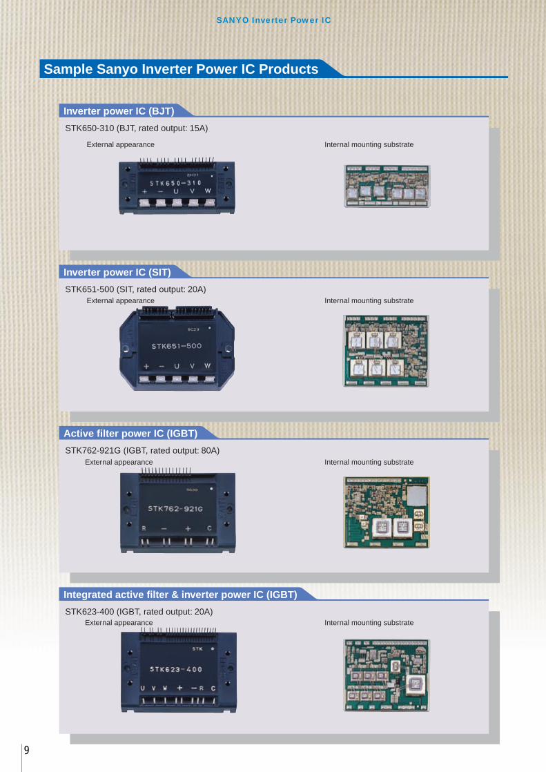
Sample Sanyo Inverter Power IC Products
SANYO Inverter Power IC
9
Inverter power IC (BJT)
Inverter power IC (SIT)
Active filter power IC (IGBT)
Integrated active filter & inverter power IC (IGBT)
STK650-310 (BJT, rated output: 15A)
STK651-500 (SIT, rated output: 20A)
STK762-921G (IGBT, rated output: 80A)
STK623-400 (IGBT, rated output: 20A) Internal mounting substrateExternal appearance
External appearance Internal mounting substrate
External appearance Internal mounting substrate
Internal mounting substrateExternal appearance
8. Features of Sanyo Inverter Power ICs
SANYO Inverter Power IC
10
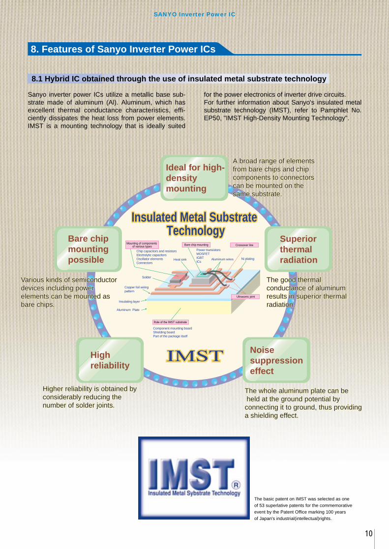
8.1 Hybrid IC obtained through the use of insulated metal substrate technology
The basic patent on IMST was selected as one of 53 superlative patents for the commemorative event by the Patent Office marking 100 years of Japan's industrial(intellectual)rights.
Sanyo inverter power ICs utilize a metallic base sub-strate made of aluminum (Al). Aluminum, which has excellent thermal conductance characteristics, effi-ciently dissipates the heat loss from power elements. IMST is a mounting technology that is ideally suited
for the power electronics of inverter drive circuits. For further information about Sanyo's insulated metal substrate technology (IMST), refer to Pamphlet No. EP50, "IMST High-Density Mounting Technology".
Ideal for high-density mounting
Bare chip mounting possible
High reliability
Noise suppression effect
Superior thermal radiation
Insulated Metal Substrate Technology
Component mounting board Shielding board Part of the package itself
Power transistorsMOSFETIGBTICs
Chip capacitors and resistors Electrolytic capacitorsOscillator elements Connectors
Copper foil wiring pattern
Insulating layer
Aluminum Plate
Aluminum wires Ni plating
Solder
Heat sink
Higher reliability is obtained by considerably reducing the number of solder joints.
The whole aluminum plate can be held at the ground potential by connecting it to ground, thus providing a shielding effect.
The good thermal conductance of aluminum results in superior thermal radiation.
Various kinds of semiconductor devices including power elements can be mounted as bare chips.
A broad range of elements from bare chips and chip components to connectors can be mounted on the same substrate.
Mounting of components of various types Bare chip mounting Crossover line
Ultrasonic joint
Role of the IMST substrate
Insulated Metal Substrate Technology
Various kinds of semiconductor devices including power elements can be mounted as bare chips.
Higher reliability is obtained by considerably reducing the number of solder joints.
The whole aluminum plate can be held at the ground potential by connecting it to ground, thus providing a shielding effect.
The good thermal conductance of aluminum results in superior thermal radiation.
A broad range of elements from bare chips and chip components to connectors can be mounted on the same substrate.
SANYO Inverter Power IC
11
8.2 Built-in protective circuits
Various protective circuits, including thermal, overcur-rent, excessive saturation voltage, short, and low sup-ply voltage protection, as well as detection elements
(shunt resistors, etc.) are mounted in a package with high-density mounting, enabling the realization of high accuracy, high stability, and high reliability.
8.3 Built-in pre-drive circuits of optimized design
Pre-drive circuits of optimized design are employed for the power output elements that are used, eliminat-ing the necessity of redesign based on consideration
of matching. As a result, the design period for embed-ded systems is shortened.
8.4 Easy intertace
Output signals from photocouplers can be used as input signals of hybrid ICs without modification. Fur-thermore, the use of high-voltage elements has ena-bled the lineup of a series (STK621-000 Series) that
does not require primary and secondary insulation through photocouplers, etc., and direct input from the microcontroller enables fast response and system min-iaturization.
8.5 High reliability
Compared to PCB mounting of discrete components, IMST hybrid ICs, which employ bare chip mounting
and aluminum wire bonding, have fewer solder joints and therefore higher reliability.
8.6 Electromagnetic shielding
Since the base substrate is made of aluminum, the hybrid IC itself is shielded. This structure is effective for the control of self noise from inverter control cir-
cuits that perform large current switching. Further-more, a cutoff effect for external noise is also obtained.
8.7 Lineup of various power element mounting types
With regard to power elements for use in IMST hybrid ICs such as Sanyo inverter power ICs, optimum series
lineups are provided to suit each application and pur-pose.
SANYO Inverter Power IC
12
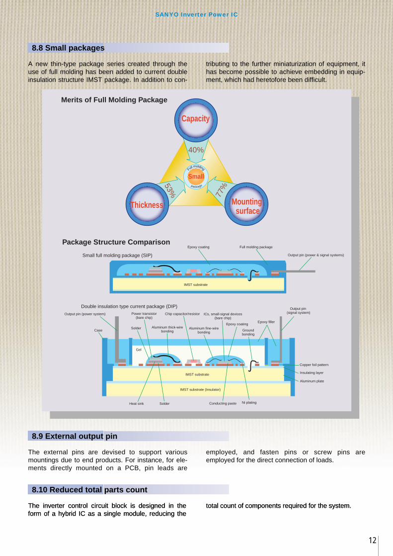
8.8 Small packages
A new thin-type package series created through the use of full molding has been added to current double insulation structure IMST package. In addition to con-
tributing to the further miniaturization of equipment, it has become possible to achieve embedding in equip-ment, which had heretofore been difficult.
8.9 External output pin
The external pins are devised to support various mountings due to end products. For instance, for ele-ments directly mounted on a PCB, pin leads are
employed, and fasten pins or screw pins are employed for the direct connection of loads.
8.10 Reduced total parts count
Chip capacitor/resistor
IMST substrate
IMST substrate (Insulator)
Aluminum thick-wire bonding
Aluminum fine-wire bonding
Ni plating
Case
Output pin (signal system)Output pin (power system)
Ground bonding
Epoxy filler Epoxy coating
Conducting paste
Solder
Gel
SolderHeat sink
Power transistor (bare chip)
ICs, small-signal devices (bare chip)
Double insulation type current package (DIP)
Copper foil pattern
Insulating layer
Aluminum plate
packageFu
ll molding
Capacity
Mounting surface
Thickness
Small
40%
53%77
%
Merits of Full Molding Package
Output pin (power & signal systems)
Full molding package
Small full molding package (SIP)
Package Structure Comparison
IMST substrate
Epoxy coating
The inverter control circuit block is designed in the form of a hybrid IC as a single module, reducing the
total count of components required for the system.The inverter control circuit block is designed in the form of a hybrid IC as a single module, reducing the
total count of components required for the system.
9. Main Characteristics
SANYO Inverter Power IC
13
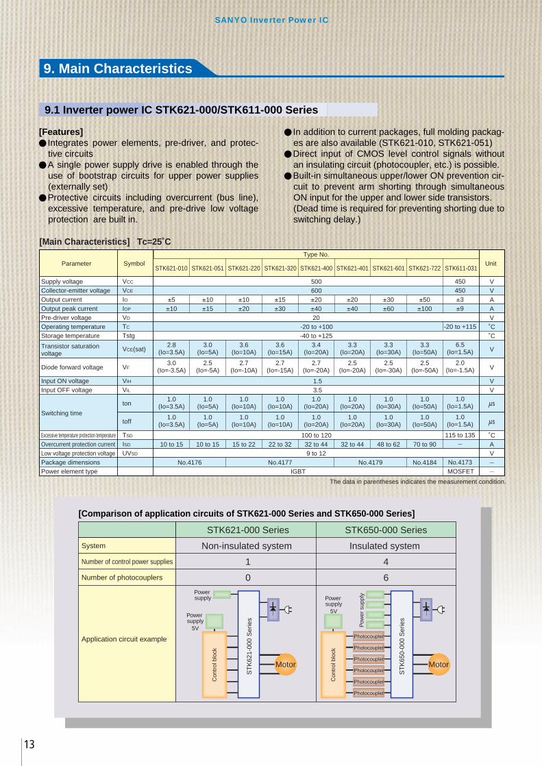
9.1 Inverter power IC STK621-000/STK611-000 Series
[Features]n Integrates power elements, pre-driver, and protec-
tive circuitsnA single power supply drive is enabled through the
use of bootstrap circuits for upper power supplies (externally set)
nProtective circuits including overcurrent (bus line), excessive temperature, and pre-drive low voltage protection are built in.
n In addition to current packages, full molding packag-es are also available (STK621-010, STK621-051)
nDirect input of CMOS level control signals without an insulating circuit (photocoupler, etc.) is possible.
nBuilt-in simultaneous upper/lower ON prevention cir-cuit to prevent arm shorting through simultaneous ON input for the upper and lower side transistors. (Dead time is required for preventing shorting due to
switching delay.)
Unit Parameter Symbol STK621-010
Supply voltage 500 450 VVCC
Collector-emitter voltage 600 450 VVCE
Output current ±5 ±10 ±10 ±15 ±20 ±20 ±30 ±50 ±3 AIOOutput peak current ±10 ±15 ±20 ±30 ±40 ±40 ±60 ±100 ±9 AIOP
Pre-driver voltage 20 VVD
Operating temperature -20 to +100 -20 to +115 ˚CTC
Storage temperature -40 to +125 ˚CTstg
STK621-051 STK621-220 STK621-320 STK621-400 STK621-401 STK621-601 STK621-722 STK611-031
Type No.
Transistor saturation voltage
2.8(Io=3.5A)
3.0(Io=5A)
3.6(Io=10A)
3.6(Io=15A)
3.4(Io=20A)
3.3(Io=20A)
3.3(Io=30A)
3.3(Io=50A)
6.5(Io=1.5A) VVCE(sat)
Diode forward voltage3.0
(Io=-3.5A)2.5
(Io=-5A)2.7
(Io=-10A)2.7
(Io=-15A)2.7
(Io=-20A)2.5
(Io=-20A)2.5
(Io=-30A)2.5
(Io=-50A)2.0
(Io=-1.5A) VVF
Input ON voltage 1.5 VVIH
Input OFF voltage 3.5 VVIL
Switching time
1.0(Io=3.5A)
1.0(Io=5A)
1.0(Io=10A)
1.0(Io=10A)
1.0(Io=20A)
1.0(Io=20A)
1.0(Io=30A)
1.0(Io=50A)
1.0(Io=1.5A) Uton
1.0(Io=3.5A)
1.0(Io=5A)
1.0(Io=10A)
1.0(Io=10A)
1.0(Io=20A)
1.0(Io=20A)
1.0(Io=30A)
1.0(Io=50A)
1.0(Io=1.5A) Utoff
Excessive temperature protection temperature 100 to 120 115 to 135 ˚CTSD
Overcurrent protection current 10 to 15 10 to 15 15 to 22 22 to 32 32 to 44 32 to 44 48 to 62 70 to 90 _ AISD
Low voltage protection voltage 9 to 12 VUVSD
Package dimensions No.4176 No.4177 No.4179 No.4184 No.4173
The data in parentheses indicates the measurement condition.
_
Power element type IGBT _MOSFET
[Main Characteristics] Tc=25˚C
[Comparison of application circuits of STK621-000 Series and STK650-000 Series]
Photocoupler
Photocoupler
Photocoupler
Photocoupler
Photocoupler
Photocoupler
Motor
Con
trol
blo
ck
Motor
0 6
1Number of control power supplies
System
Number of photocouplers
Application circuit example
4
Non-insulated system Insulated system
STK621-000 Series STK650-000 Series
ST
K62
1-00
0 S
erie
s
ST
K65
0-00
0 S
erie
s
Power supply
Pow
er s
uppl
y
Power supply
5V
Power supply
5V
Con
trol
blo
ck

SANYO Inverter Power IC
14
[Equivalent Circuit Diagram]
-
+
VB1U
VB2V
VB3W
HIN1HIN2HIN3
LIN1LIN2LIN3
Shunt-Resistor
VBSU.V.
VBSU.V.
VBSU.V.
LevelShifter
Latch Reset (All Input = High)Overcurrent Over-Temp.
VDD-UnderVoltage
Logic Logic Logic
LevelShifter
LevelShifter
FAULTISO
VDD
VSS
-
+
VB1U
VB2V
VB3W
HIN1HIN2HIN3
LIN1LIN2LIN3
VBSU.V.
VBSU.V.
VBSU.V.
LevelShifter
LatchOver-Temp.
VDD-UnderVoltage
Logic Logic Logic
LevelShifter
LevelShifter
FAULT
VDD
VSS
Reset (All Input = High)
STK612-000 Series STK611-000 Series
STK611-000 Series STK612-000 Series
[Sample Application Circuit]
CI
CS
VCC+
-
CB
DB
CB
DB
CB
RB
DB
STK621-000 Series
CD
VD4
Motor
Control Logic(+5V)
CI
CS
VCC+
-
CB
DB
CB
DB
CB
RB
DB
STK611-000 Series
CD
VD4
Motor
Control Logic(+5V)

SANYO Inverter Power IC
15
9.2 Inverter power IC STK650-000/STK651-000 Series
[Features]n Integrates power elements, pre-driver, and protec-
tive circuits nEmploys low-saturation bipolar transistors for the
power output stage to realize low loss (STK650-000 Series). Moreover, products further realizing ultra-low loss are also available through the use of the SIT process (STK651-000 Series).
nProtective circuits including overcurrent (bus line),
excessive temperature, and excessive saturation voltage protection are built in.
nLoads are easily connected thanks to the use of fasten pins for the power system output pins.
nControl signals can be supported at the logic level through the use of photocouplers.
nSeries offering pin compatibility from 15A to 30A. The power capacitance can be changed by simply replac-ing hybrid ICs, enabling standardized set design.
[Main Characteristics] Tc=25˚C
Unit Parameter Symbol
Supply voltage 450400 VVCC
Output current 20 AIOOutput peak current 40 AIOP
Pre-drive voltage 5.5 to 8.0 7.5 to 10.0 5.5 to 8.0 VVD1 to VD4Operating temperature -30 to +100 ˚CTC
Storage temperature -40 to +125 ˚CTstg
STK651-500
Type No.
Collector-to-emitter sustain voltage 500 VVCEX(sus)
Collector-to-emitter reverse voltage VVF
Switching time
Uton
Utstg
Excessive temperature protection temperature 100 to 120 ˚CTSD
Overcurrent protection current 25 to 31 AISD
Excessive saturation voltage protection level 15 VVSD
Package drawing No.4178 No.4180 No.4181
The data in parentheses indicates the measurement condition.
_
Power element type BJT SIT _
STK650-610STK650-510STK650-430STK650-410STK650-310
3060
600(ICEX=8mA)
2.5(Io=-30A)
2(Io=30A)
2(Io=30A)
2550
2.5(Io=-25A)
2(Io=25A)
5(Io=-25A)
8(Io=-30A)
2(Io=25A)
2040
2.5(Io=-20A)
2(Io=20A)
5(Io=-20A)
2(Io=20A)
2040
2.5(Io=-20A)
2(Io=20A)
5(Io=-20A)
2(Io=20A)
1530
500(ICEX=6mA)
2.5(Io=-15A)
4
1
Collector-to-emitter saturation voltage VVCE(sat)5
(Io=30A)
3.5(Io=20A)
1(Io=20A)
3(Io=20A)
5(Io=25A)
5(Io=20A)
5(Io=20A)
5(Io=15A)
2(Io=15A)
5(Io=-15A)
2(Io=15A) Utr
40 to 4827 to 3322 to 2722 to 2718 to 23
[Equivalent Circuit Diagram] [Sample Application Circuit]
* * * *
W V UUVWTRIP
VCC+
-
STK650-000/STK651-000 Series
VD1
VD2
VD3
VD4
Motor
*Only the STK650-610 require Zener diodes.
VD1UIN
RB1GND1
VD2VIN
RB2GND2
VD3WIN
RB3
+
UGND3
VD4
UIN
RB4GND4
VIN
WIN
TRIP
Overcurrent protection (ISD) Excessive temperature protection (TSD)
V
W
-
SANYO Inverter Power IC
16
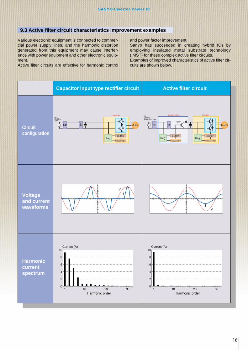
9.3 Active filter circuit characteristics improvement examples
Various electronic equipment is connected to commer-cial power supply lines, and the harmonic distortion generated from this equipment may cause interfer-ence with power equipment and other electronic equip-ment. Active filter circuits are effective for harmonic control
and power factor improvement. Sanyo has succeeded in creating hybrid ICs by employing insulated metal substrate technology (IMST) for these complex active filter circuits. Examples of improved characteristics of active filter cir-cuits are shown below.
Buffer
Motor
Reg.
NF
BufferReg.
Inverter Inverter AC 50/60Hz100V
AC 50/60Hz85 to 240V Free
Active filter
NF
BufferReg.
MicrocontrollerMicrocontroller Microcontroller
Motor
VI
VI
1 100
2
4
6
8
10Current (A)
Harmonic order 20 30 1 10
0
2
4
6
8
10Current (A)
Harmonic order 20 30
Capacitor input type rectifier circuit Active filter circuit
Voltage and current waveforms
Harmonic current spectrum
Circuit configuration

SANYO Inverter Power IC
17
9.4 Active filter power IC STK762-000G Series
[Features]n Integrates the major circuits of active filters (power
elements, FRD, current detection resistors, control IC, protective circuits)
nUses IGBT for power elements nHigh power factor through the use of average cur-
rent control system nDirect output voltage can be controlled over a wide
range (Approx. 160 to 385V during AC100V input) n Built-in overcurrent, excessive temperature, and
overvoltage protection circuits
[Main Characteristics] Tc=25˚C
UnitParameter Symbol
Supply voltage 600 VVCE
Output current AICOutput peak current AICP
FRD reverse voltage 600 VVRM
FRD forward current 40 AIFFRD forward voltage 3 (IF=40A) V
20 V
VF
Type No.
Control supply voltage VCC
25 30 mAControl power supply current drain during operation ICC ON
100 to 120 ˚CExcessive temperature protection temperature TSD
6850 AOvercurrent protection current ISD
3020 ArmsBooster coil current ICOIL
160 to 385 VDCDirect current output voltage Vout
-20 to +100 ˚COperating temperature TC
-40 to +125 ˚CStorage temperature Tstg
No.4182 _Package dimensions
The data in parentheses indicates the measurement condition.
STK762-721G STK762-921G
80160
4080
[Equivalent Circuit Diagram] [Sample Application Circuit]
Current detection resistor
IGBTFRD
Operation setting signal (output voltage, oscillation frequency, reference waveform, overvoltage setting)
Control power supply
(Vcc=17V)
Protection operation output
Soft start/Boost operation enable input
Control reference voltage/oscillation
frequency
R
C
-
+
Excessive temperature Overcurrent protection
Soft start circuit
PFC control IC
CSSfOSCOUT
CVC
Crf
CiCZ
Cf
Inductor
ENBL
TRIP
AC Input
STK762-000G Series
Inverter power IC
STK621-000 Series, etc.
VCC
Motor
(Application to inverter circuit)
ROL
RVL
RPH
RPLRT
RML
CMM
RMM
RMH
ROH
RSI
RVH CT

SANYO Inverter Power IC
18
9.5 Integrated active filter & inverter power IC STK623-000 Series
[Features]n Integrates an active filter (PFC) circuit for power fac-
tor improvement and a 3-phase inverter circuit that can be driven with a single power supply.
n Inverter block: IGBT for power elements adopted. Driving with a single power supply is made possible
through the bootstrap system using a level shift cir-cuit in the high voltage pre-driver block.
Built-in overcurrent, excessive temperature, and low control power supply voltage protection circuits
nActive filter (PFC) block: IGBT for power elements adopted Built-in control IC (average current control type),
FRD, current detection resistors, soft start circuit, overcurrent and overvoltage protection circuits
nThe direct current output voltage of the active filter block can be set externally (PAM control supported)
[Main Characteristics] Tc=25˚C
Unit Parameter Symbol
Inverter blockSupply voltage 1 VVCE1Output current AIoOutput peak current AIOP
Control supply voltage 1 VVD1 to VD4Maximum loss (IGBT) W
V
Pd
Type No.
FWD forward voltage VF1
100 to 12025
˚CExcessive temperature protection temperature TSD
AOvercurrent protection current ISD
9 to 12 VLow pre-drive supply voltage protection level UVSD
600 V
Active filter blockVCE2Supply voltage 2
40 AICOutput current
600 VVRDFRD reverse voltage
±402036
Upper transistor 3.0 / Lower transistor 3.5 (Io=-20A)
VVsupplyControl supply voltage 2
3 (IF2=40A) VVF2FRD forward voltage
mAIonControl circuit current drainCommon block
450 VRectification output voltage VCC
15 ArmsBooster coil current ICOIL
160 to 385 VDCDirect current output voltage Vout
-20 to +100 ˚COperating temperature TC
-40 to +125 ˚CStorage temperature Tstg
No.4183 _Package dimensions
The data in parentheses indicates the measurement condition.
STK623-400
600±20
20
15
[Equivalent Circuit Diagram] [Sample Application Circuit]
CiCL
CD4CS
CB
DB
CB
DB
CB
DBRTRU
RB
RO
RH RP RD
RQ
RE
CrCT
CZ
Inductor
AC Input
STK623-000 Series
VD4(15V)
Vsup(17V)
Motor
Control Logic(+5V)
(during drive with 1 power supply)
PWM signalOperation setting signal (voltage, frequency, reference waveform)
FAULT signal 15V power supply (INV block)
17V power supply
(PFC block)
R
C - + U V W
Bootstrap input (upper phase power supply)
Temperature/current protectionPFC control IC
High voltage pre-driver + low supply voltage protection

SANYO Inverter Power IC
19
9.6 Triac power IC STK630-000 Series
[Main Characteristics] Tc=25˚C
[Features]nMulti-triac hybrid IC for AC power switch built in pre-
driver n Ideal for AC switches of washing machines, dryers,
heated toilet seats, etc. nThe power output block can be configured as 1
package, so that the standardization of parts is pos-sible. Moreover, more compact and thin sets can be designed.
nThe STK630-010 (under development) consists of
an AC switch block (other than motor) for inverter washing machine and a power supply block com-bined into 1 package.
nThe use of a low thermal resistant IMST substrate results in superior heat dissipation and enables the elimination of heat sinks.
nThe use of hollow structure packages, which make smoke emission and fires less likely, results in supe-rior safety.
Unit Parameter Signal
Repetitive peak off-state voltage VVDRM
Effective ON current AIT(RMS)
Power supply output current mAIo1
Type No.
Io2
up to 0.8at least 4.0
up to 0.4at least 0.8
VInput ON voltage VIH
VInput OFF voltage VIL
[Power supply circuit not built in] VPower supply output voltageVo1
Vo2
-20 to +100 ˚CTCOperating temperature
-40 to +125 ˚CTstgStorage temperature
No.4175 No.4185 No.4174_Package dimensions
6006008
[Power supply circuit not built in]
Under developmentSTK630-010 STK630-252 STK630-255A STK630-260 (D) STK630-261 (D)
5 built-in circuits 6 built-in circuits 5 built-in circuits 5 built-in circuits 5 built-in circuits3 circuits
50up to 0.4
200
14.5 to 16.54.7 to 5.3
at least 0.8
4001
3 circuits
3
1 circuits
1
4 circuits60010
2 circuits400 600 (800) 600 (800)
1
3 circuits
8
2 circuits
1
3 circuits
10
2 circuits
1
3 circuits
[Equivalent Circuit and Sample Application Circuit]
STK630-010
Inverter power IC
STK621-000 Series, etc.
Motor
Zero-cross circuit
AC Input85 to 264V
Triac output block
Pre-driver Microcontroller
DC-DC converter Reg.
15.5V 5V
VDDGND
U
UVB3 VB2 VB1
V
W-
+
V W U V W
INT
Feed valve, drain valve, etc. 3A output x 1 1A output x 4
(In case of use in inverter washing machine)

20
Package dimensions 4173
Package dimensions 4174
Package dimensions 4175
Package dimensions 4176
Package dimensions 4177
10. Package Dimensions
539
2152=42
22
221
21
0.5
0.4
5.2
7.5
5.5
31.1
160.
5
3.9
70
2.54
1 22
R2.3
0.5
2.5
5.5
4.6
78
2.54521=53.34
5.6
67
9
0.4
5.2
60
231
2--3.6
(8)
0.5
2252=44
2
11
16
25.5
13.2
8.5
0.4
2.9
16.5 21
328
78
70
27
2
1
0.5
(9) 2652=5.2
2--ø3.6
22
4--ø2.78 deep
2--ø4.4hole
4--ø1protrusion 0.5
2--R3
2.54
8
1
0.5
2152.54=53.34
61
1
4--hollow 1
73
87
1
7
14
48
2--73
1354=52
77.5
23 29
16.2
50.
416
.25
11
84
37
CA
IT
IMS
T + - U V W
21
Package dimensions 4178
22
4--ø2.78 deep
2--ø4.4hole
7
A
4--ø1protrusion 0.5
2--R3
7.5
DETAILE A
C1
ø1.65hole
6.35
2.54
8
1
0.5
2152.54=53.34
61
P=12
hollow 1
73
87
2--73
77.5
48
23 29
16.2
5
0.4
16
0.8
11
10
3.47.
95
4
37
CA
IT
IMS
T
Package dimensions 4180
22
4--ø2.78 deep
2--ø4.4hole
5
A
4--ø1protrusion 0.5
2--R3
7.5
DETAILE A
C1
ø1.65 hole
6.35
2.54
8
1
0.5
2152.54=53.34
61
P=12
4-- 1
73
87
2--73
77.5
48
23 29
26.5
0.4
26.2
5
0.8
11
10
3.47.
95
4
57.5
CA
IT
IMS
T
Package dimensions 4179
22
4--ø2.78 deep
2--ø4.4hole
5
4--ø1protrusion 0.5
2--R3
2.54
1
0.5
2152.54=53.34
61
1
4--hollow 1
73
87
1 14
4
52
23 29
(26.
5)
0.4
8
0.4
(26.
5)
11
84
57.5
CA
IT
IMS
T
77.5
2--73
53
Package dimensions 4181
22
A
10
4.5
DETAILE A
C1ø1.65 hole
6.35
7.5
2.5852.5=20 1152.5=27.5
1
52.5
124512=48
77.5
2526
.3
0.8
0.65
11 7.5 3.
47.95
57.5
ø4.4
CA
IT
IMS
T
+ - U V W
+ - U V W
+ - U V W
+ - U V W

22
Package dimensions 4182
22
4--ø2.78 deep
2--ø4.4hole
5
4--ø1protrusion 0.5
2--R3
2.54
1
0.5
2152.54=53.34
61
1
4--hollow 1
73
87
1 14
4
52
23 29
26.5
0.4
8
0.4
26.5
11
84
57.5
CA
IT
IMS
T
77.5
2--73
- + CR
Package dimensions 4184
A
10
2
8
DETAILE A
C1ø1.65 hole
6.35
7.5
2.54
22
100
1
0.5
2152.54=53.34
89
6015
2230
.5
0.8
0.4
11.5
5
3.47.
95
6654
ø4.4
IMS
TC
AIT
Package dimensions 4183
28
11
8
4--ø1 protrusion 0.5
2--ø4.4 hole
4--ø
2.7
8 de
ep
2
1
87
0.5
54
61
1
73
29 42
4
52
23 29
26.5
0.4
0.4
26.5
84
57.5
CA
IT
IMS
T
73
73
U V W + - R C
Package dimensions 4185
8.5
2.54
55.6
31
21
16.5
64
1 18
(6.21) 1752.54=43.18
0.5
2--ø3.6
(R0.4 to 0.8)
(R0.4 to 0.8)
34
5.2
DETAILE
0.4
7
U V W+ -

<Any and all SANYO products described or contained herein do not have specifications that can
handle applications that require extremely high levels of reliability, such as life-support systems,
aircraft's control systems, or other applications whose failure can be reasonably expected to
result in serious physical and/or material damage. Consult with your SANYO representative
nearest you before using any SANYO products described or contained herein in such
applications.
<SANYO assumes no responsibility for equipment failures that result from using products at
values that exceed, even momentarily, rated values (such as maximum ratings, operating
condition ranges, or other parameters) listed in products specifications of any and all SANYO
products described or contained herein.
<Specifications of any and all SANYO products described or contained herein stipulate the
performance, characteristics, and functions of the described products in the independent state,
and are not guarantees of the performance, characteristics, and functions of the described
products as mounted in the customer's products or equipment. To verify symptoms and states
that cannot be evaluated in an independent device, the customer should always evaluate and
test devices mounted in the customer's products or equipment.
<SANYO Electric Co., Ltd. strives to supply high-quality high-reliability products. However any
and all semiconductor products fail with some probability. It is possible that these probabilistic
failures could give rise to accidents or events that could endanger human lives that could give
rise to smoke or fire or that could cause damage to other property. When designing equipment,
adopt safety measures so that these kinds of accidents or events cannot occur. Such measures
include but are not limited to protective circuits and error prevention circuits for safe design,
redundant design, and structural design.
<In the event that any or all SANYO products (including technical data, services) described or
contained herein are controlled under any of applicable local export control laws and regulations,
such products must not be exported without obtaining the export license from the authorities
concerned in accordance with the above law.
<No part of this publication may be reproduced or transmitted in any form or by any means,
electronic or mechanical, including photocopying and recording, or any information storage or
retrieval system, or otherwise, without the prior written permission of SANYO Electric Co., Ltd.
<Any and all information described or contained herein are subject to change without notice due
to product/technology improvement, etc. When designing equipment, refer to the "Delivery
Specification" for the SANYO product that you intend to use.
<Information (including circuit diagrams and circuit parameters) herein is for example only; it is not
guaranteed for volume production. SANYO believes information herein is accurate and reliable,
but no guarantees are made or implied regarding its use or any infringements of intellectual
property rights or other rights of third parties.
Printed in Japan / September 2000 3k AVJ
For technical information, please contact :
<JAPAN SANYO ELECTRIC CO.,LTD. SEMICONDUCTOR Tokyo Bldg., 1-10, 1-chome, Ueno, Taito-ku, Tokyo 110-8534 Japan Tel:81(Country Code)-3-3837-6339,6340,6342, Fax:81-3-3837-6377
<HONGKONG SANYO SEMICONDUCTOR (H.K.) CO., LTD. Room 612, Harbour Crystal Centre, 100 Granville Road, Tsimshatsui East, Kowloon, Hong Kong Tel:852-2311-1198, Fax:852-2311-0900, Tlx:56370 SSCHK HX
SHIN-NICHI ELECTRONICS DEVICE (H.K.) LTD. Room 2001, Park-in Commercial Center, 56 Dundas Street, Kowloon, Hong Kong Tel:852-2388-3434, Fax:852-2780-2401
PROTECH PERENNIAL LTD. Unit 4, 3/F., Wah Shing Center, 11 Shing Yip Street, Kwun Tong, Kowloon, Hong Kong Tel:852-2950-2338, Fax:852-2950-2828
OS ELECTRONICS (H.K.) LTD. Room 2111, Peninsula Tower, 538 Castle Peak Road, Cheung Sha Wan, Kowloon, Hong Kong Tel:852-2741-2218, Fax:852-2786-5733
TONG SAN ELECTRONIC (H.K.) CO., LTD. Room 01B12, 23/F., Nan Fung Centre, 264-298 Castle Peak Road, Tsuen Wan, N.T., Hong Kong Tel:852-2415-3988, Fax:852-2415-8823
<CHINA SANYO SEMICONDUCTOR(H.K.)CO.,LTD. Shanghai Liaison Office : Room 2407, Ruijing Building, No.205 Maoming South Road, Shanghai, 200020 P.R.C. Tel:86-21-6472-7674, Fax:86-21-6472-7556
SANYO SEMICONDUCTOR (H.K.) CO., LTD. Guangzhou Liaison Office : Room 1351, China Hotel Commercial Tower, Liuhua-Lu, Guangzhou, 510015 P.R.C. Tel:86-20-8667-7450, Fax:86-20-8667-5072
<SINGAPORE SANYO SEMICONDUCTOR (S) PTE., LTD. 750D Chai Chee Road #05-04 to 06 Chai Chee Industrial Park Singapore 469004 Tel:65-442-1226, Fax:65-442-1280
SANYO SEMICON DEVICE CO., LTD. Singapore Branch : 221 Henderson Road #08-11 Henderson Industrial Park, Singapore 159557 Tel:65-275-4775/4776, Fax:65-275-4548
OS ELECTRONICS (S) PTE., LTD. 33 Tannery Lane #05-00 Hoesteel Building, 347789 Singapore Tel:65-746-7770, Fax:65-746-3500/1691
SHIN-NICHI ELECTRONICS (S) PTE., LTD. 25 Tagore Lane #02-07, Singapore Godown, Singapore 787602 Tel:65-552-8996, Fax:65-552-8830/8846
<MALAYSIA SANYO SEMICONDUCTOR (S) PTE., LTD. KL Regional Office : 504, Block A, Level 5 Kelana business Centre, Off subang Airport Highway 97 Jalan SS 7/2, 47301 Petaling Jaya Selangor Darul Ehsan, Malaysia Tel:60-3-5828822, Fax:60-3-5828823
SANYO SEMICONDUCTOR (S) PTE., LTD. Penang Regional Office : Unit 15-C2, Menara BHL Bank 51, Jalan Sultan Ahmad Shah 10050 Penang, Malaysia Tel:60-4-226-6877, Fax:60-4-227-6877
<KOREA SANYO SEMICONDUCTOR (H.K.) CO., LTD. Seoul Branch : Room #1201 Samjung Bldg., 69-5, 2-Ka, Taepyong-Ro, Chung-ku, Seoul, 100-102 Korea Tel:82-2-774-0296, Fax:82-2-752-9790, Tlx:SILICON K22920
SHIN-NICHI ELECTRONICS CO., LTD. Seoul Liaison Office : 3F Gohoun Bldg., 646-18 Yoksam-dong, Kangnam-gu, Seoul, Korea Tel:82-2-508-2812, Fax:82-2-508-2814
PAIK YOUNG ELECTRONICS CO., LTD. 162-1, 2-Ka, Jangchung-Dong, Chung-ku, Seoul, Korea 3F, Taekwang Bldg., Tel:82-2-277-8431/279-7857,7858, Fax:82-2-268-1158
YANG WON ENTERPRISE CO., LTD. 700-5 Daelim-Dong Young Dongpo-ku, Seoul Korea Tel:82-2-843-2888, Fax:82-2-846-6885
<TAIWAN SANYO SEMICONDUCTOR TAIPEI CO., LTD. Room #706, Chia Hsin Bldg., 96, Chung Shan Road, N.SEC.2, Taipei, Taiwan, R.O.C. 104 Tel:886-2-2551-5886, Fax:886-2-2541-7649
SANYO SEMICONDUCTOR TAIPEI CO., LTD. Kaohsiung Office : Room 603, 61. Chung 3rd Road, Kaohsiung, TAIWAN, R.O.C. 806 Tel:886-7-332-5703, Fax:886-7-332-6647
TONG SAN ELECTRIC CO., LTD. Room 406, No.372 Lin Sen N.Road, Taipei, Taiwan, R.O.C. 104 Tel:886-2-2561-0381, Fax:886-2-2543-5431, Tlx:23588 TONSANCO
OS SEMICONDUCTOR CO., LTD. 3rd.Fl, No.145, Sec.2, Minsheng E.Road, Taipei, Taiwan, R.O.C. 104 Tel:886-2-2515-2286, Fax:886-2-2516-2388
<UNITED KINGDOM SANYO SEMICONDUCTOR (EUROPE) GmbH UK Office : Unit1, Walton Lodge, Bridge Street, Walton-on Thames, Surrey KT12 1BT, United Kingdom Tel:44-1932-233-600, Fax:44-1932-230-104
<GERMANY SANYO SEMICONDUCTOR (EUROPE) GmbH Office Center Schwalbach 1, Am Kronberger Hang 2a 65824 Schwalbach am Taunus, Germany Tel:49-6196-926-0, Fax:49-6196-926-266
SHIN-NICHI ELECTRONICS CO., LTD. Europe Liaison Office : Carl-Zeiss-Ring 3 D-85737 Ismaning, München, Germany Tel:49-89-420494-6, Fax:49-89-420494-74
<U.S.A. SANYO SEMICONDUCTOR CORPORATION New Jersey Office : 80 Commerce Drive, Allendale, NJ 07401, U.S.A. Tel:1-201-825-8080, Fax:1-201-825-0163, Tlx:135138 SANYOSEMI ALNJ
SANYO SEMICONDUCTOR CORPORATION California Office : 2010 N.1st Street, Suite 500, San Jose, CA 95131, U.S.A. Tel:1-408-441-6567, Fax:1-408-441-6672
SANYO SEMICONDUCTOR CORPORATION Illinois Office : 900 N. Arlington Heights Road, Suite 360 Itasca, Illinois 60143, U.S.A. Tel:1-630-775-0006, Fax:1-630-775-0060
SANYO SEMICONDUCTOR CORPORATION San Diego Office : 2055 sanyo Avenue, San Diego, CA 92173, U.S.A. Tel:1-619-661-4880, Fax:1-619-661-4881
SANYO SEMICONDUCTOR DISTRIBUTION (U.S.A.) CORPORATION 49 Walnut Street, Norwood, New Jersey 07648, U.S.A. Tel:1-201-784-0303, Fax:1-201-784-8003
80100
TOKYO OFFICE Tokyo Bldg., 1-10, 1 Chome, Ueno, Taito-ku, TOKYO, 110-8534 JAPAN Telephone:03-3837-6339, 6340, 6342, Facsimile:03-3837-6377

![HYDROVARHYDROVAR Power supply Output to motor Type Rated output Voltage limits 48-62 Hz Recommended Rated current line protection Max. voltage output output HV [kW] [V] [A] [V] [A]](https://img.pdfslide.us/doc/110x75/60b9368db7874e2ac643ec24/hydrovar-hydrovar-power-supply-output-to-motor-type-rated-output-voltage-limits.jpg)


![GLSV-035 series - MPL Power · GLSV - 035 B xxx Series name Rated Output Power [W] Option name 012 – rated output voltage is 12V 024 – rated output voltage is 24V 036 – rated](https://img.pdfslide.us/doc/110x75/5ebc32ca3243bb12635f5334/glsv-035-series-mpl-power-glsv-035-b-xxx-series-name-rated-output-power-w.jpg)


![FRENIC AQUA INGLES - Fuji Electric Europe... [kV Rated input current [A] ... 4.3 3.0 2.2 110 4.0 132 4.0 6.8 9 0 7.4 5. 2 5.5 10 13 ... motor (rated (rated output) output) [kW] [kW]](https://img.pdfslide.us/doc/110x75/5aa2fc567f8b9ac67a8dce28/frenic-aqua-ingles-fuji-electric-kv-rated-input-current-a-43-30-22.jpg)


![0.4 Amp Output Current IGBT Gate Drive Optocoupler1].pdf0.4 Amp Output Current IGBT Gate Drive Optocoupler Technical Data HCPL-J314 Features • 0.4 A Minimum Peak Output Current •](https://img.pdfslide.us/doc/110x75/5e2014e1c1dcd664806d227d/04-amp-output-current-igbt-gate-drive-1pdf04-amp-output-current-igbt-gate-drive.jpg)