Embed Size (px)
Citation preview
OptoelectronicsEE/OPE 451, OPT 444
Fall 2009 Section 1: T/Th 9:30‐ 10:55 PM
John D. Williams, Ph.D.
Department of Electrical and Computer Engineering
406 Optics Building ‐ UAHuntsville, Huntsville, AL 35899
Ph. (256) 824‐2898 email: [email protected]
Office Hours: Tues/Thurs 2‐3PM
JDW, ECE Fall 2009

PHOTOVOLTAIC DEVICES
Prentice‐Hall Inc.© 2001 S.O. KasapISBN: 0‐201‐61087‐6http://photonics.usask.ca/
• 6.1 Solar Energy Spectrum
• 6.2 Photovoltaic Device Principles
• 6.3 pn Junction Photovoltaic I‐V Characteristics
• 6.4 Series Resistance and Equivalent Circuit
• 6.5 Temperature Effects
• 6.6 Solar Cells Materials, Devices and Efficiencies
JDW, ECE Fall 2009

Blackbody Radiation• Definition of a black body: An object that
absorbs all radiation incident upon it
• The energy absorbed by a blackbody is then emitted in a temperature dependent spectrum of light, called thermal radiation which is primarily in the infrared spectrum
• Blackbody radiation is characterized by three fundamental equations
– Plank’s Law – blackbody absorption curve
– Wien’s Law ‐ characteristic wavelength of the blackbody
– Stefan‐Boltzmann Law ‐ energy radiated from the blackbody as a function of temperature
1
18),( 3
3
−=
kTh
echTU ννπν
428
4
1067.5
*
KmW
Tj
−⋅=
=
σ
σ
TKm ⋅⋅
=−3
max101.5λ 0
0 5 10 15 20 25 30 35
Intensity (arbitrary)
Wavelength (um)
Blackbody RadiationT = 100 K
T = 200 K
T = 300 K
T = 400 K
T = 500 K
λmax = 25.5μm
λmax = 10.2μm
λmax = 12.8μm
λmax = 17.0μm
J(100K)=5.67 W/m2
J(200K)=90.7 W/m2
J(300K)=1450 W/m2
J(400K)=3540 W/m2
J(500K)=17900 W/m2JDW, ECE Fall 2009

Photovoltaic Basics
• Photovoltaic cells convert incident solar radiation energy into electrical energy
• Thus these devices are used as energy harvesters and converters
• The goal is to convert as much incident photon energy as possible into electrical energy
• To do this, one must have a measure of what incident energy is available
• The figure presented shows three curves– First, is the ideal blackbody spectrum of a 6000K
heat source that such as the sun
– The red curve represents the actual available solar energy above the earth’s atmosphere
– The green curve represents the actual available solar energy at the earth’s surface
– Absorption of radiation in the atmosphere constitutes the difference between AM0 and AM1.5
JDW, ECE Fall 2009

Solar Energy• Light intensity variation with wavelength is generally represented by Spectral Intensity which is Iλ = I/λ
(intensity/wavelength)
• The total intensity over a spectral range is given by
• The integrated intensity above the earths atmosphere, gives the total power flow through a unit area perpendicular to the direction of the sun. This quantity is called the solar constant (air‐mass zero) or AM0 radiation and is approximately 1.353 kW/m2
• Actual intensity on the earth’s surface depends on absorption and scattering in the atmosphere. The effects of water vapor (clouds) in the air provide a general value of solar intensity at the surface that is approximately 70% of AM0 with specific bands that are reduced significantly due to water and nitrogen absorption. The received spectrum is called Air Mass 1 ( AM1)
∫=2
1
λ
λ
λIdI
Direct Diffuse
(a) Illustration of the effect of the angle of incidence θ on the ray path length and the
definitions of AM0, AM1 and AM(secθ). The angle α between the sun beam and the horizon
is the solar latitude (b) Scattering reduces the intensity and gives rise to a diffused radiation
Atmosphere
AM0
AM1
θ
AM(secθ)
h0h
α
(a) (b)
α
Tilted PV deviceEarth
© 1999 S.O. Kasap, Optoelectronics (Prentice Hall)
• Generically, Air Mass m (AMm) is defined as the ratio of actual radiation path to shortest possible path through an atmosphere. So for light entering an atmosphere at angle θ
• However, diffusive scattering plays a significant role as well, and the ratio of scattered light and scattering angles should also be taken into account
θθ
θ
secsec
/)sec(/ 00
AMAMmm
hhhhm o
==
==
JDW, ECE Fall 2009

Example: Solar Energy Conversion• Suppose that a particular household consumes 500 W of electrical power daily• If the average solar intensity incident per day is 6kW h/m2, a photovoltaic device that converts
solar energy into electrical energy has a 15% efficiency, then what is the required device area to meet the electrical needs of the home.
Since we know that the avg. light intensity incident ,
Total energy available per day = incident solar energy in 1 day per unit area X area X efficiency
Which must be equal to the total energy consumed in the household per day
Area = energy per house / (incident solar energy per unity area X efficiency)
the required panel size is 3.6 m X 3.6 m
NOTE: This solution does not account for heavy clouds, rain, or excess consumption!!!!
2
2
3.1315.0/36006000
24/3600500 mhrs
daymhrW
hrhrsWArea =⋅⋅⎟⎟
⎠
⎞⎜⎜⎝
⎛ ⋅⋅⋅
=
JDW, ECE Fall 2009

Photovoltaic Device Principles• Consider a pn junction with a very narrow and heavily doped n‐
region at the top surface• Light passes through the n‐region and is absorbed in the
depletion region which can take up a vast majority of the thickness of the device.
• The built‐in Field, Eo in the depletion region drives EHP to their respective electrode
• Finger electrodes are often used to optimize surface area while still providing uniform contact across large areas of the photovoltaic
• Thin antireflection coatings on the surface are also used to prevent excess reflection and improve efficiency
• The open circuit voltage in the system driven by the built‐in field and photoabsorbed EHP carriers provides a bias that one can draw off the device
• Mobility in the device– Long wavelength photons generate electrons in the p‐
type neutral region that must drift diffuse using the diffusion coefficient of the material to n‐type region
– Medium wavelength photons generate EHP in the depletion region yielding electron transit times based on carrier mobility in the electric field
– Short wavelength photons generate holes in the n‐region that must drift diffuse to the depletion region where they are driven by hole carrier mobility to the neutral p‐type region
Finger electrodes
p
n
Bus electrodefor current collection
Finger electrodes on the surface of a solar cellreduce the series resistance
© 1999 S.O. Kasap, Optoelectronics (Prentice Hall)

• In steady state, there can be no net current through an open circuit solar cell. Thus the number of carriers of each type must be balanced. (conservation of charge)
• To insure against recombination losses, N is very short (0.2 um or less)
• For λ = 1‐ 1.2 um in Si, the penetration depth is typically larger than 100 um and p‐side thicknesses are 200‐ 500 um. This gives a long minority carrier diffusion length and a wide depletion zone for mid wavelength absorption
• Si bandgap = 1.2 EV which corresponds to a cutt‐off of 1.1 um, so energy at lambda greater than 1.1 um is wasted, which is about 25% of the thermal energy available at room temperature
• Furthermore losses to do EHP recombinations at the surface can be as high as 40%.
• In addition the antireflective coating is never perfect, reducing the total number of collected photons down by about 9%
• Now including limitations of the photovoltaic device itself that will be discussed throughout the chapter, the efficiency of a Si solar cell is no higher than 26%
LeLh W
Iph
x
EHPs
exp(−αx)
Photogenerated carriers within the volume Lh + W + Le give rise to a photocurrent Iph. Thevariation in the photegenerated EHP concentration with distance is also shown where α is thabsorption coefficient at the wavelength of interest.
© 1999 S.O. Kasap, Optoelectronics (Prentice Hall)
Photovoltaic Device Principles

Example: Photocurrent
• Consider a photovoltaic device that is illuminated with light of such wavelength that photogeneration occurs over the device thickness.
– Assume an EHP photogeneration rate of Gphwhich decays spatially as Goexp(‐αx), where Go is the surface photogeneration rate and α is the absorption coefficient.
– Let us suppose that the device is shortened to allow carriers to flow around the external circuit. Also suppose that Lh is greater than the n‐layer thickness, ln so that all EHPS generated within the volume of the device contribute to photocurrent.
– Finally assume that recombination near the surface of the crystal is negligible.
• Find the photocurrent in the system
( )[ ]{ }( )[ ]{ }
( )enoph
LWloEHPph
LWloEHP
LWlx
x
xoen
LWlAeGIsmalliswavlengthslongFor
eAeGdt
dNeI
eAGdt
dN
dxeGALWlintimeunitperEHP
en
en
en
++=⇒
−==
−=
=++
++−
++−
++=
=
−∫
___,__
1
1
_____0
α
α
αα
α
α
Silicon ExampleA = 5 cm X 5 cmLn = 0.5 μmW =2 μmLe =50 μmGo = 1 x 1018 cm3/s
α= 2000/m (δ = 500 μm) λ= 1.1 μmIph = 20 mA
α= 105/m (δ = 10 μm) λ= 0.83 μmIph = 40 mA
λ < 0.45 μmThen α= 1X10⁶/m (δ = 0.5 μm)Iph = 0.2 mAJDW, ECE Fall 2009

Pn junction Photovoltaic I‐V Characteristics
• Consider an ideal pn photovoltaic connected to a resistive load
• If the circuit is short circuited, then only current generated by incident light is present. We define this as photocurrent.
• The greater the light intensity, the more EHPs generated, the higher the photocurrent
• The short circuit current is found to be
where K is a device constant
• The photocurrent does not depend on a bias across the junction, because there is always some internal field to drift EHPs across the diode.
• Note: we exclude the secondary effect of voltage modulating the width of the device and assume a large spectral bandwidth
• Therefore photocurrent flows without a forced bias as long as light is present
• IF R is not a short, then a positive bias appears across the junction resulting from the built in potential, Vo of the pn junction.KIII phsc −==
JDW, ECE Fall 2009
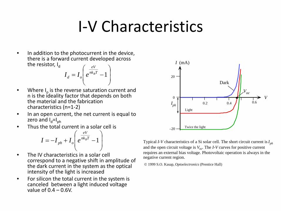
I‐V Characteristics• In addition to the photocurrent in the device,
there is a forward current developed across the resistor, Id
• Where Io is the reverse saturation current and n is the ideality factor that depends on both the material and the fabrication characteristics (n=1‐2)
• In an open current, the net current is equal to zero and Id=Iph
• Thus the total current in a solar cell is
• The IV characteristics in a solar cell correspond to a negative shift in amplitude of the dark current in the system as the optical intensity of the light is increased
• For silicon the total current in the system is canceled between a light induced voltage value of 0.4 – 0.6V.
⎟⎟⎠
⎞⎜⎜⎝
⎛−= 1Tnk
eV
odBeII
⎟⎟⎠
⎞⎜⎜⎝
⎛−+−= 1Tnk
eV
ophBeIII
V
I (mA)
Dark
Light
Twice the light
0.60.40.2
20
–20
0Iph
Voc
Typical I-V characteristics of a Si solar cell. The short circuit current is Iphand the open circuit voltage is Voc. The I-V curves for positive currentrequires an external bias voltage. Photovoltaic operation is always in thenegative current region.© 1999 S.O. Kasap, Optoelectronics (Prentice Hall)

The Load Line• Consider again a solar cell connected to a resistive load, R.
– R maintains the same voltage as the solar cell– R carries the same current as the solar cell– However the current through R travels in the opposite
direction of conventional current. The current in this circuit passes from low to high potential
I = ‐V/R• The actual current and voltage in the circuit must satisfy
both the solar cell IV curve and that of the load. A graphical solution is presented here
– Easiest method of solution is to construct a “load line” with the slope = ‐1/R
– The load line intercepts the solar cell IV curve at point ‘P’ where the load and the solar cell have the same voltage and current
– Point ‘P’ satisfies both governing conditions and represents the operating point of the circuit.
– The power delivered to the load is Pout =I’V’– The goal of any circuit design is to optimize R within Isc
and Voc such that when illuminated, one generates the maximum power output available from the load
– One figure of merit is the fill factor (FF) which gives the designer a quick measure of the closeness of the solar cell IV curve to a square shape and thus allows one to quickly identify the optimal resistive that need be applied
ocsc
mm
VIVIFF =
– One figure of merit is the fill factor (FF) which gives the designer a quick measure of the closeness of the solar cell IV curve to a square shape and thus allows one to quickly identify the optimal resistive that need be applied
JDW, ECE Fall 2009

Example: Open Circuit Voltage and Illumination
• A solar cell is illuminated with intensity 600 W/m2 and has a short circuit current, Isc = 16.1 mA and an open circuit voltage, Voc = 0.485 V. What are the short circuit current and open circuit voltages when the light intensity is doubled?
( )( )
( ) VII
eTnkVV
nthateconvienencforassumenext
mAmAIIII
II
eTnk
II
eTnkVV
II
eTnkV
theneTnkV
assume
eIII
set
Bococ
scsc
B
ph
phBococ
o
phBoc
Boc
TnkeV
ophB
503.0)2ln(0259.01485.0ln
1____
2.3221.16
lnln
ln
/
01
1
212
1
212
1
2
1
212
=+=⎟⎟⎠
⎞⎜⎜⎝
⎛+=
=
==⎟⎟⎠
⎞⎜⎜⎝
⎛=
⎟⎟⎠
⎞⎜⎜⎝
⎛=⎟
⎟⎠
⎞⎜⎜⎝
⎛=−
⎟⎟⎠
⎞⎜⎜⎝
⎛=
>>
=⎟⎟⎠
⎞⎜⎜⎝
⎛−+−=
V
I (mA)
Dark
Light
Twice the light
0.60.40.2
20
–20
0Iph
Voc
Typical I-V characteristics of a Si solar cell. The short circuit current is Iphand the open circuit voltage is Voc. The I-V curves for positive currentrequires an external bias voltage. Photovoltaic operation is always in thenegative current region.© 1999 S.O. Kasap, Optoelectronics (Prentice Hall)
JDW, ECE Fall 2009

Example: A Solar Cell Driving a Resistive Load
• Consider a solar cell driving a 30 Ω load. Suppose the cell has an area of 1 cm X 1 cm and is illuminated with light of intensity Io = 600 W/m2 and has the IV characteristics shown in the figure below.
– What are the current and voltage in the circuit?
– What is the power delivered to the load?
– What is the efficiency of the solar cell in the circuit?
( )( )
( )( )
%06.10100
6001.0/600
035.6425.02.14''
2.1430425.0'
425.0'30
22
==
==
===
=Ω
−≈
≈Ω
−=
in
out
in
out
PP
efficiencymWmmWP
recallmWVmAVIP
mAVI
VV
VI
η
JDW, ECE Fall 2009

Series Resistance and Equivalent Circuit
• Along with the load resistance, RL• One must also consider the effective series
resistance of electrons traveling along the surface of the solar cell prior to reaching the finger electrode, RS
• There are also a much smaller series resistances due to the neutral p‐type region that also contribute to Rs
• We know the photocurrent process is represented by a constant current generator Iphwhere current is proportional to light intensity
• And we know that the normal diode current flows opposite of the photcurrent
• There is also the possibility for carriers to flow through the crystal surfaces or grain boundaries (polysilicon devices) instead of through the external load. These effects are represented by an internal parallel resistance, Rp
– Typically Rp is less important than Rs unless the device is highly polycrystalline
Neutraln-region
Neutralp-region
Fingerelectrode
Backelectrode
Depletionregion
RL
Rs
Rp
Series and shunt resistances and various fates of photegenerated EHPs.© 1999 S.O. Kasap, Optoelectronics (Prentice Hall)
A
Iph Rp RLV
IIph
Id
Solar cell LoadB
Rs
The equivalent circuit of a solar cell© 1999 S.O. Kasap, Optoelectronics (Prentice Hall)
JDW, ECE Fall 2009
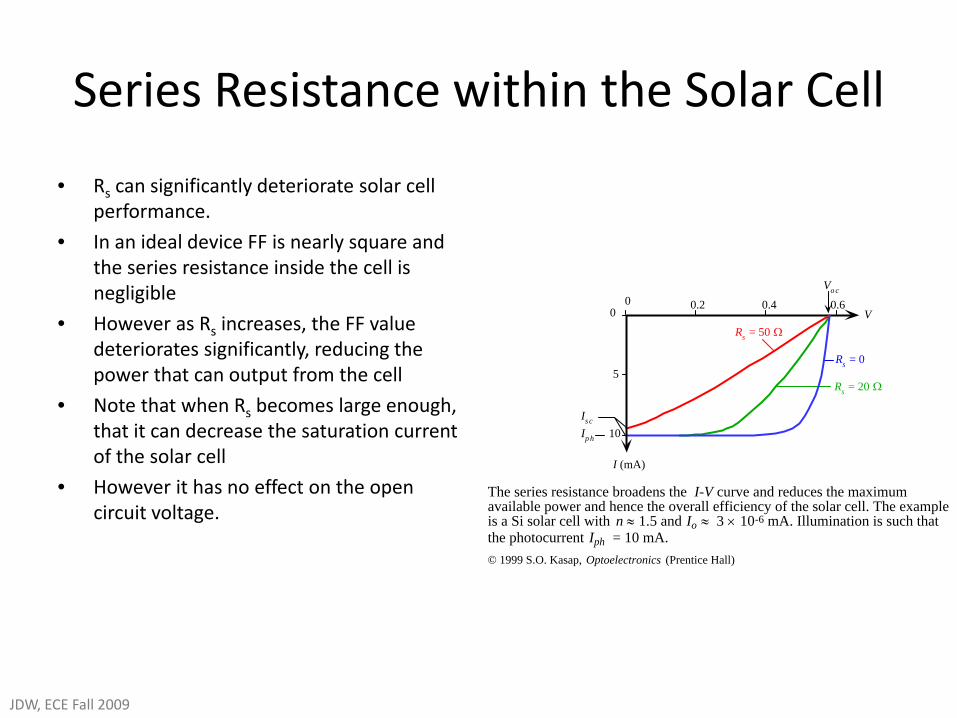
Series Resistance within the Solar Cell
• Rs can significantly deteriorate solar cell performance.
• In an ideal device FF is nearly square and the series resistance inside the cell is negligible
• However as Rs increases, the FF value deteriorates significantly, reducing the power that can output from the cell
• Note that when Rs becomes large enough, that it can decrease the saturation current of the solar cell
• However it has no effect on the open circuit voltage.
I (mA)
V0
00.2 0.4 0.6
5
10
Vo c
Isc
Rs = 0
Rs = 20 Ω
Rs = 50 Ω
Ip h
The series resistance broadens the I-V curve and reduces the maximumavailable power and hence the overall efficiency of the solar cell. The exampleis a Si solar cell with n ≈ 1.5 and Io ≈ 3 × 10⁻⁶ mA. Illumination is such thatthe photocurrent Iph = 10 mA.© 1999 S.O. Kasap, Optoelectronics (Prentice Hall)
JDW, ECE Fall 2009

Example: Solar Cells in Parallel• Consider two identical solar cells with Io = 25 nA, n = 1.5, Rs =
20 Ω. Both cells are subjected to the same illumination such that Iph = 10 mA.
• Explain the characteristics of the two cells connected in parallel
• Find the Maximum power that can be delivered by one cell and two cells in series and also the corresponding voltage and current at the maximum power point if Rp = ∞
0.60.40.20246
5
15
Voltage (V)Power (mW)
Current (mA)
20
10
1 cell
2 cells in parallel
Current vs. Voltage and Power vs. Current characteristics of one cell and twocells in parallel. The two parallel devices have Rs/2 and 2 Iph. © 1999 S.O. Kasap, Optoelectronics (Prentice Hall)
A
IphV
Iph
Id
B
Rs
RL
I/2
Id
Iph
I
RsI/2
Two identical solar cells in parallel under the same illumination anddriving a load RL.© 1999 S.O. Kasap, Optoelectronics (Prentice Hall)
( )
Ω≈⇒−=
≈≈⇒
⎟⎟⎠
⎞⎜⎜⎝
⎛−+−=⎟
⎟⎠
⎞⎜⎜⎝
⎛−+−=
−
34/
27.0,8,2.2
11
:__
max
RRVIfrom
VVmAImWP
eIIeIII
celloneFor
TnkIRVe
ophTnk
eV
ophB
s
B
d
Ω≈
≈≈⇐=
⎟⎟⎟
⎠
⎞
⎜⎜⎜
⎝
⎛
−+−=⎟⎟⎠
⎞⎜⎜⎝
⎛−+−=
⎟⎠⎞⎜
⎝⎛ −
17
27.0,164.4
________
tan___2/1_
________
112
___
2
Ryielding
VVmAImWP
currentsaturationreversethedoublehasntphotocurrethedoublehas
ceresisseriesthehas
devicethethatseesonetwotheComparing
eIIeIII
hasdeviceseachSeriesIn
II
Tnk
IRVe
ophTnk
eV
ophB
s
B
d
JDW, ECE Fall 2009
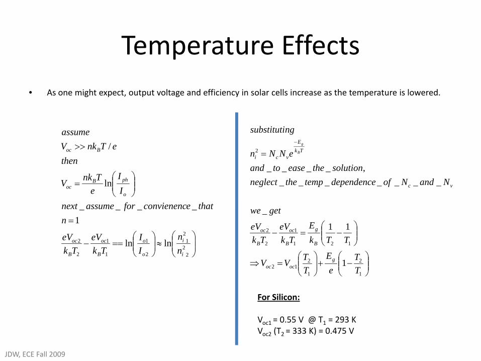
Temperature Effects• As one might expect, output voltage and efficiency in solar cells increase as the temperature is lowered.
⎟⎟⎠
⎞⎜⎜⎝
⎛≈⎟⎟
⎠
⎞⎜⎜⎝
⎛==−
=
⎟⎟⎠
⎞⎜⎜⎝
⎛=
>>
22
12
2
1
1
1
2
2 lnln
1____
ln
/
i
i
o
o
B
oc
B
oc
o
phBoc
Boc
nn
II
TkeV
TkeV
nthateconvienencforassumenext
II
eTnkV
theneTnkV
assume
For Silicon:
Voc1 = 0.55 V @ T1 = 293 KVoc2 (T2 = 333 K) = 0.475 V
⎟⎟⎠
⎞⎜⎜⎝
⎛−+⎟⎟
⎠
⎞⎜⎜⎝
⎛=⇒
⎟⎟⎠
⎞⎜⎜⎝
⎛−=−
=−
1
2
1
212
121
1
2
2
2
1
11
_
_______,____
TT
eE
TTVV
TTkE
TkeV
TkeV
getwe
NandNofdependencetemptheneglectsolutiontheeasetoand
eNNn
ngsubstituti
gococ
B
g
B
oc
B
oc
vc
TkE
vciB
g
JDW, ECE Fall 2009

Solar Cell Materials, Devices, And Efficiencies
• Most solar cells are silicon based due to the vast infrastructure and inexpensive fabrication schemes available
• The figure presented shows how various aspects of a silicon solar cell effect its efficiency
• Note: some 25% of all the incident energy is wasted because of photons having insufficient energy to generate EHPs
• Of the 75% of light absorbed, only 60% of the is effectively utilized due to near surface absorption in the n‐region
• etc. etc. etc.
JDW, ECE Fall 2009

Surface Shaping of Solar Cells to Improve Light Collection
• Reduces reflections from surface
• Increases path length for absorption and improves EHP and collection efficiencies
JDW, ECE Fall 2009

III‐V Materials for Thermal Photovoltaics
• Heterojunction devices used to overcome surface recombination limitations and improve efficiencies to as much as 24%
• Wider bandgaps provide longer wavelength absorbtion
• AlGaAs absorb hv > 2eV
• GaAs absorb 1.4 eV <hv < 2eV
• In more advanced cell designs, the composition of Al is graded slowly from the surface allowing the device to absorb the broad spectrum between 1.4 and 2.0 eVmore evenly.
• Tandem cells designed to absorb short wavelength light at the top pn junction and longer wavelength light below it improve EHP efficiencies while maintaining high FF values for the device
p-AlGaAs window (< 0.02 μm
p-GaAs
n-GaAs
Passivated GaAs surface
AlGaAs window layer on GaAs passivates the surface statesand thereby increases the low wavelength photogenerationefficiency© 1999 S.O. Kasap, Optoelectronics (Prentice Hall)
np
Cell 1 (Eg1) Cell 2 (Eg2 < Eg1)
n p
Connecting region.
A tandem cell. Cell 1 has a wider bandgap and absorbs energeticphotons with hυ > Eg1. Cell 2 absorbs photons that pass cell 1 andhave hυ > Eg2.
© 1999 S.O. Kasap, Optoelectronics (Prentice Hall)JDW, ECE Fall 2009


![S A OPE 19 U A E 19 OPE 196 T · 2020-03-09 · A I SP L A S A U A E OPE 9HQH]XHOD OPE OPE OPE T T T A I IR I SP L A N U A E S A 196 191 199 196 2000 196 19 196 200 19 OPE 196 P E](https://img.pdfslide.us/doc/110x75/5eb193773ed8566dce459833/s-a-ope-19-u-a-e-19-ope-196-t-2020-03-09-a-i-sp-l-a-s-a-u-a-e-ope-9hqhxhod-ope.jpg)