Embed Size (px)
Citation preview
12
Optoelectronic Device using a Liquid Crystal Holographic Memory
Minoru Watanabe Shizuoka University,
Japan
1. Introduction
Recently, the technologies related to liquid crystal spatial light modulators have progressed dramatically [1]–[4]. Such modulators are classifiable as two types: transmissive and reflective. Both types are used widely for various applications, e.g. liquid crystal television panels, personal computer displays, and projector systems. In particular, the resolution of
the latest liquid crystal spatial light modulators in projectors has reached 1,920 pixels × 1,080
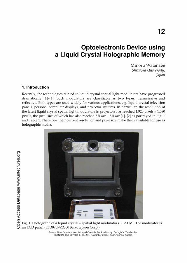
pixels, the pixel size of which has also reached 8.5 μm × 8.5 μm [1], [2] as portrayed in Fig. 1 and Table 1. Therefore, their current resolution and pixel size make them available for use as holographic media.
Fig. 1. Photograph of a liquid crystal – spatial light modulator (LC-SLM). The modulator is an LCD panel (L3D07U-81G00 Seiko Epson Corp.) O
pen
Acc
ess
Dat
abas
e w
ww
.inte
chw
eb.o
rg
Source: New Developments in Liquid Crystals, Book edited by: Georgiy V. Tkachenko, ISBN 978-953-307-015-5, pp. 234, November 2009, I-Tech, Vienna, Austria
New Developments in Liquid Crystals
220
LCD type L3D07U-81G00
Resolution 1,920 x 1,080
Panel size 0.7 inch
Pixel pitch 8.5 μ m
Aperture ratio 55 %
Table 1. Specifications of the L3D07U-81G00 LC-SLM Panel.
Moreover, recently, optically reconfigurable gate arrays (ORGAs) with a holographic memory have been developed [5]–[7], [11]–[14], [21]–[23]. The gate array of this optoelectronic device has a fine grain gate array structure similar to those of field programmable gate arrays (FPGAs) [8]–[10]. Computations or circuit operations on the gate array are executed electrically, as they are on FPGAs, whereas configurations and reconfigurations for the gate array are optically executed. The ORGA architecture has features of rapid reconfiguration and numerous reconfiguration contexts. Such an optical reconfiguration architecture often uses liquid crystal spatial light modulators as holographic memory media [11]–[14], [21]–[23]. Therefore, this chapter first presents the characteristics of a liquid crystal holographic memory to generate binary patterns. In addition, as an illustration of one application of liquid crystal devices, this chapter presents discussion of the research of optically reconfigurable gate arrays (ORGAs).
2. Transmissive-type computer-generated hologram
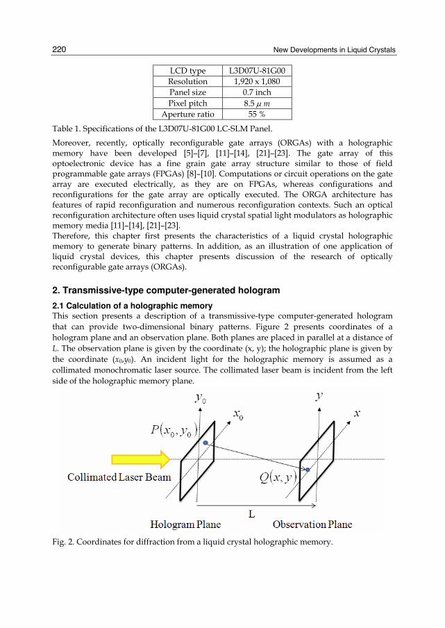
2.1 Calculation of a holographic memory This section presents a description of a transmissive-type computer-generated hologram
that can provide two-dimensional binary patterns. Figure 2 presents coordinates of a
hologram plane and an observation plane. Both planes are placed in parallel at a distance of
L. The observation plane is given by the coordinate (x, y); the holographic plane is given by
the coordinate (x0,y0). An incident light for the holographic memory is assumed as a
collimated monochromatic laser source. The collimated laser beam is incident from the left
side of the holographic memory plane.
Fig. 2. Coordinates for diffraction from a liquid crystal holographic memory.
Optoelectronic Device using a Liquid Crystal Holographic Memory
221
Here, a two-dimensional binary pattern on the observation plane is assumed to be given as a
function O(x,y), which represents a configuration or reconfiguration context in optically
reconfigurable gate arrays (explained later). At that time, the intensity distribution of a
holographic medium is calculable using the following equations.
0 0
2( , ) ( , )sin( ) ,H x y O x y r dxdy
πλ
∞ ∞−∞ −∞∝ ∫ ∫
2 2 2
0 0= ( ) ( ) .r L x x y y+ − + − (1)
In those equations, λ signifies the wavelength, L signifies the distances between the
holographic plane and the observation plane, and r stands for the distance between the
point source 0 0( , )P x y on the holographic memory plane and the point of observation
( , )Q x y . The distance L is expected to take ( 1 / 4)n λ+ , where n is an arbitrary natural
number, to receive the perpendicular incident beam on the observation plane efficiently
with the shortest distance from the holographic memory plane. The value 1 1( , )H x y is
normalized as 0–1 for the minimum intensity minH and maximum intensity maxH , as shown
below.
0 00 0
( , )( , ) = .min
max min
H x y HH x y
H H
−′ − (2)
Finally, the normalized image H ′ is used for implementing a holographic memory.
2.2 Diffraction from a holographic memory Next, the diffraction pattern is estimated from the above calculated holographic memory
pattern. The complex light distribution at the coordinate (x, y) are calculated using the
following equations as
0 0 0 0
2( , ) ( , )exp( ) ,
Y Xmax max
Y Xmin min
u x y H x y i r dx dyπλ− − ′∝ ∫ ∫
2 2 2
0 0= ( ) ( ) ,r L x x y y+ − + − (3)
where 0 0( , )H x y′ denotes the calculated and normalized holographic memory pattern, λ
represents the wavelength, L stands for the distances between the holographic plane and the
observation plane, and Xmax, Xmin, Ymax, and Ymin respectively represent the holographic
memory sizes. Finally, the diffraction intensity from a holographic memory is calculable as
*( , ) = ( , ) ( , ),I x y u x y u x y (4)
where the superscript asterisk denotes the complex conjugate.
2.3 Single bright bit example in the Fresnel region In this section, once again, the holographic memory pattern described in section 2.1 is
treated, but in the Fresnel region. If distance L between the two coordinate planes can be
New Developments in Liquid Crystals
222
assumed to be large compared with the sizes of a holographic memory and observation
area, when the following condition is satisfied,
{ }22 2 3
0 0
1( ) ( ) << ,
4x x y y Lλ − + − (5)
then r can be approximated to
2 2
0 0( ) ( ),
2
x x y yr L
L
− + −+0 (6)
where (x0,y0) is the coordinate of the holographic memory plane and (x,y) is the coordinate
of the observation plane. Here, assuming that the condition L= ( 1 / 4)n λ+ (n = an arbitrary
natural number) is satisfied, then ( 1 / 4)n λ+ can be substituted into the first term L of Eq. 6
shown above. Then, substituting Eq. 6 with the condition into Eq. 1, the following equation is accomplished.
{ }2 2
0 0 0 0( , ) ( , )cos ( ) ( ) .H x y O x y x x y y dxdyL
πλ
∞ ∞−∞ −∞
⎛ ⎞∝ − + −⎜ ⎟⎝ ⎠∫ ∫ (7)
Assuming that the single bright bit is located on the coordinate ( , )α β , the equation O(x,y)
can be considered as ( , )x yδ α β− − . The two-dimensional Dirac delta function ( , )x yδ is
defined as shown below.
, = = 0
( , ) =0,
for x yx y
otherwiseδ ∞⎧⎨⎩ (8)
and
( , ) = 1.x y dxdyδ∞ ∞−∞ −∞∫ ∫ (9)
When ( , ) = ( , )O x y x yδ α β− − , Eq. 7 can be simplified to the following equation.
{ }2 2
0 0 0 0( , ) cos ( ) ( ) .H x y x yL
π α βλ⎛ ⎞∝ − + −⎜ ⎟⎝ ⎠ (10)
The maximum and minimum of the above equation are, respectively, 1 and -1. Therefore, the above equation can be substituted into Eq. 2. Finally, the following equation of a holographic memory pattern including a single bright bit in Fresnel region can be derived.
{ }2 2
0 0 0 0
1 1( , ) = cos ( ) ( ) .
2 2H x y x y
L
π α βλ⎛ ⎞′ − + − +⎜ ⎟⎝ ⎠ (11)
This equation represents a Fresnel zone lens, the center of which is located at coordinate
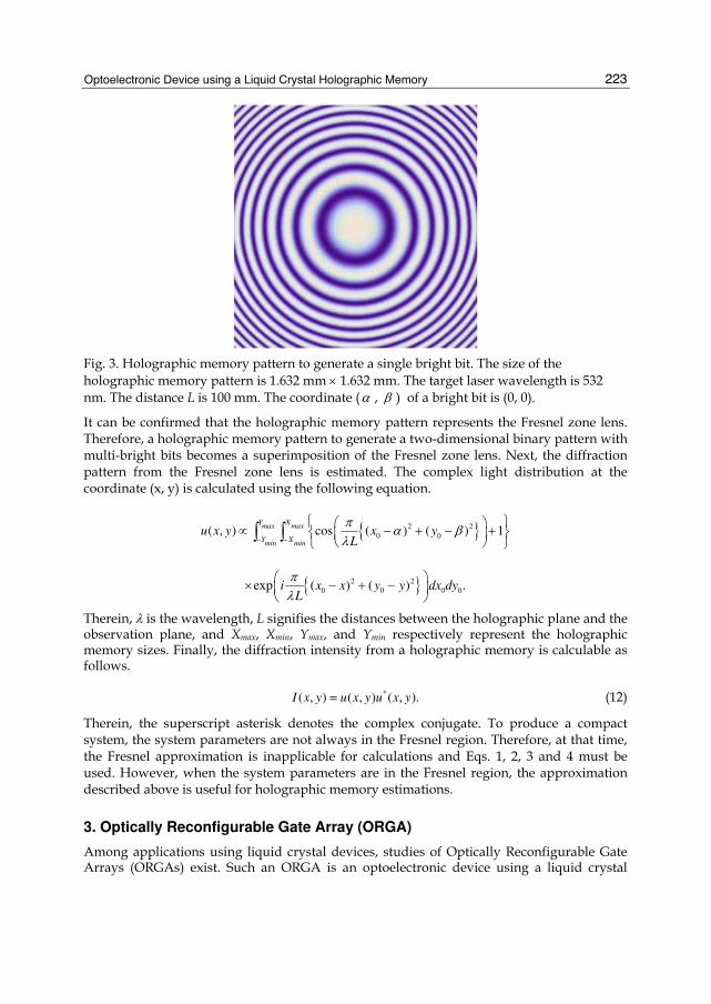
( , )α β . An example of a holographic memory of size of 1.632 mm × 1.632 mm to generate a
single bright bit is shown in Fig. 3. In this example, the holographic memory pattern was calculated using the condition that the target laser wavelength is 532 nm, the distance L is
100 mm, and the coordinate (α , β ) of a bright bit is (0, 0).
Optoelectronic Device using a Liquid Crystal Holographic Memory
223
Fig. 3. Holographic memory pattern to generate a single bright bit. The size of the
holographic memory pattern is 1.632 mm × 1.632 mm. The target laser wavelength is 532
nm. The distance L is 100 mm. The coordinate (α , β ) of a bright bit is (0, 0).
It can be confirmed that the holographic memory pattern represents the Fresnel zone lens. Therefore, a holographic memory pattern to generate a two-dimensional binary pattern with multi-bright bits becomes a superimposition of the Fresnel zone lens. Next, the diffraction pattern from the Fresnel zone lens is estimated. The complex light distribution at the coordinate (x, y) is calculated using the following equation.
{ }2 2
0 0( , ) cos ( ) ( ) 1Y Xmax max
Y Xmin min
u x y x yL
π α βλ− −⎧ ⎫⎛ ⎞∝ − + − +⎨ ⎬⎜ ⎟⎝ ⎠⎩ ⎭∫ ∫
{ }2 2
0 0 0 0exp ( ) ( ) .i x x y y dx dyL
πλ
⎛ ⎞× − + −⎜ ⎟⎝ ⎠
Therein, λ is the wavelength, L signifies the distances between the holographic plane and the observation plane, and Xmax, Xmin, Ymax, and Ymin respectively represent the holographic memory sizes. Finally, the diffraction intensity from a holographic memory is calculable as follows.
*( , ) = ( , ) ( , ).I x y u x y u x y (12)
Therein, the superscript asterisk denotes the complex conjugate. To produce a compact system, the system parameters are not always in the Fresnel region. Therefore, at that time, the Fresnel approximation is inapplicable for calculations and Eqs. 1, 2, 3 and 4 must be used. However, when the system parameters are in the Fresnel region, the approximation described above is useful for holographic memory estimations.
3. Optically Reconfigurable Gate Array (ORGA)
Among applications using liquid crystal devices, studies of Optically Reconfigurable Gate Arrays (ORGAs) exist. Such an ORGA is an optoelectronic device using a liquid crystal
New Developments in Liquid Crystals
224
device as a holographic memory. This device is being developed as an alternative device of current VLSIs or as a next-generation general-purpose programmable VLSI. The following section presents a description of the ORGA background and architecture.
3.1 Background In recent years, SRAM-based Field Programmable Gate Arrays (FPGAs) have been used widely for large-item small-volume production because of their flexible programmable capabilities [8]–[10]. Moreover, demand for high-speed reconfigurable devices has been increasing. If circuit information can be downloaded rapidly from a configuration memory, idle circuits on a gate array can be removed. At that time, other necessary circuits can be downloaded from the configuration memory into the gate array, thereby increasing the gate array's activity. In so doing, high-speed dynamic reconfiguration can increase the performance of programmable gate arrays. However, since reconfiguration of FPGAs requires more than several milliseconds, FPGAs are unsuitable for use as dynamically reconfigurable devices [8]–[10]. However, high-speed reconfigurable devices have been developed: DAP/ DNA chips, DRP chips, and multi-context FPGAs [15]–[20]. Those devices package reconfiguration memories and microprocessor arrays or gate arrays onto a chip. The internal reconfiguration memory stores reconfiguration contexts of 4–16 banks, which can be changed from one to another on a clock. Consequently, the arithmetic logic unit or gate array of such devices can be reconfigured on every clock cycle in a few nanoseconds. Nevertheless, an important problem remains: simultaneously increasing the internal reconfiguration memory while maintaining the gate density is extremely difficult. For that reason, optically reconfigurable gate arrays (ORGAs) [5]–[7], [11]–[14], [21]–[23]
have been developed to provide two capabilities: rapid reconfiguration and numerous
reconfiguration contexts. Such optical reconfiguration architecture often uses liquid crystal
spatial light modulators as a holographic memory [11]–[14], [21]–[23]. This chapter presents
a description of the studies of ORGAs with a liquid crystal spatial light modulator.
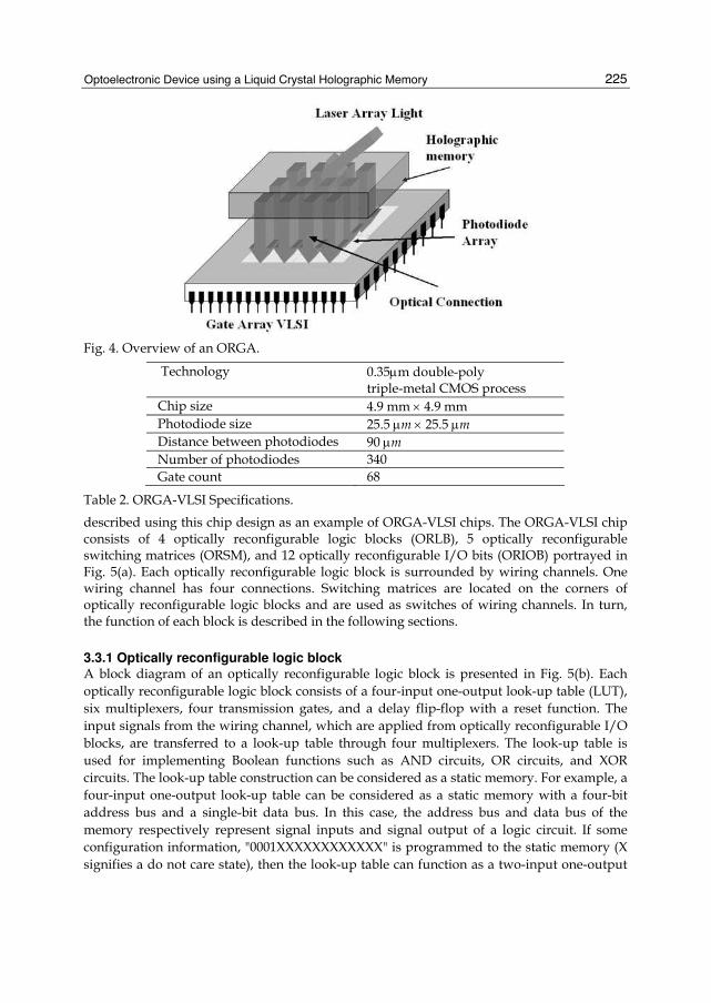
3.2 Entire construction An overview of an Optically Reconfigurable Gate Array (ORGA) is shown in Fig. 4. An ORGA consists of a gate-array VLSI (ORGA-VLSI), a holographic memory, and a laser diode array. The holographic memory can store numerous reconfiguration contexts. A laser array mounted on the top of the holographic memory addresses the reconfiguration contexts. The diffraction pattern from the holographic memory can be received as a reconfiguration context on a photodiode-array of a programmable gate array on an ORGA-VLSI. Such ORGA architecture enables microsecond-order reconfiguration and multiple reconfiguration contexts. Therefore, virtually, the architecture can achieve gate counts larger than the physical gate count on a VLSI.
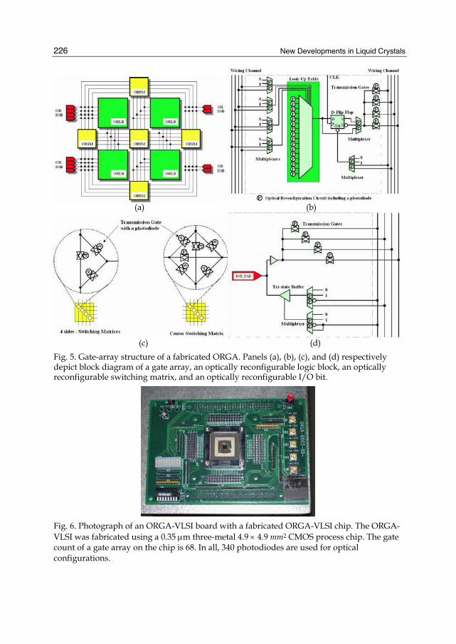
3.3 Gate array structure The basic functionality of an ORGA-VLSI is fundamentally identical to that of currently available field programmable gate arrays (FPGAs). Figure 5 depicts the gate array structure
of a first prototype ORGA-VLSI. The ORGA-VLSI chip was fabricated using a 0.35 μm triple-metal CMOS process [12]. A photograph of the board is portrayed in Fig. 6. The specifications are presented in Table 2. Here, the fundamental function of an ORGA-VLSI is
Optoelectronic Device using a Liquid Crystal Holographic Memory
225
Fig. 4. Overview of an ORGA.
Technology
0.35μm double-poly triple-metal CMOS process
Chip size 4.9 mm × 4.9 mm
Photodiode size 25.5 μm × 25.5 μm
Distance between photodiodes 90 μm
Number of photodiodes 340
Gate count 68
Table 2. ORGA-VLSI Specifications.
described using this chip design as an example of ORGA-VLSI chips. The ORGA-VLSI chip consists of 4 optically reconfigurable logic blocks (ORLB), 5 optically reconfigurable switching matrices (ORSM), and 12 optically reconfigurable I/O bits (ORIOB) portrayed in Fig. 5(a). Each optically reconfigurable logic block is surrounded by wiring channels. One wiring channel has four connections. Switching matrices are located on the corners of optically reconfigurable logic blocks and are used as switches of wiring channels. In turn, the function of each block is described in the following sections.
3.3.1 Optically reconfigurable logic block A block diagram of an optically reconfigurable logic block is presented in Fig. 5(b). Each
optically reconfigurable logic block consists of a four-input one-output look-up table (LUT),
six multiplexers, four transmission gates, and a delay flip-flop with a reset function. The
input signals from the wiring channel, which are applied from optically reconfigurable I/O
blocks, are transferred to a look-up table through four multiplexers. The look-up table is
used for implementing Boolean functions such as AND circuits, OR circuits, and XOR
circuits. The look-up table construction can be considered as a static memory. For example, a
four-input one-output look-up table can be considered as a static memory with a four-bit
address bus and a single-bit data bus. In this case, the address bus and data bus of the
memory respectively represent signal inputs and signal output of a logic circuit. If some
configuration information, "0001XXXXXXXXXXXX" is programmed to the static memory (X
signifies a do not care state), then the look-up table can function as a two-input one-output
New Developments in Liquid Crystals
226
(a) (b)
(c) (d)
Fig. 5. Gate-array structure of a fabricated ORGA. Panels (a), (b), (c), and (d) respectively depict block diagram of a gate array, an optically reconfigurable logic block, an optically reconfigurable switching matrix, and an optically reconfigurable I/O bit.
Fig. 6. Photograph of an ORGA-VLSI board with a fabricated ORGA-VLSI chip. The ORGA-
VLSI was fabricated using a 0.35 μm three-metal 4.9 × 4.9 mm2 CMOS process chip. The gate count of a gate array on the chip is 68. In all, 340 photodiodes are used for optical configurations.
Optoelectronic Device using a Liquid Crystal Holographic Memory
227
AND circuit. In this case, two multiplexers connected to upper two bits of the look-up table must be programmed to be L. The multiplexers connected to the inputs of look-up table can choose L, H, and two signals of the wiring channel for the look-up table inputs. In addition, the output of the look-up table is connected to a multiplexer through a delay type flip-flop. Therefore, a combinational circuit and sequential circuit can be chosen by changing the multiplexer. Finally, an output through the multiplexer from the look-up table is connected to the wiring channel through transmission gates, again. The last multiplexer controls the reset function of a delay-type flip-flop. Such a four-input one-output look-up table, each multiplexer, and each transmission gate respectively have 16 photodiodes, two photodiodes, and one photodiode. In all, 32 photodiodes are used for programming an optically reconfigurable logic block. In Fig. 5(b), the P mark shows a photodiode. In this optically reconfigurable logic block, although eight other photodiodes were implemented for special use of a differential reconfiguration strategy, that method is described in earlier reports [12], [21].
3.3.2 Optically reconfigurable switching matrix Similarly, optically reconfigurable switching matrices are optically reconfigurable. A block
diagram of the optically reconfigurable switching matrix is portrayed in Fig. 5(c). The basic
construction is the same as that used by Xilinx Inc. One four-directional with 24
transmission gates and 4 three-directional switching matrices with 12 transmission gates
were implemented in the gate array. In this construction, a connection in any direction can
be realized using a transmission gate so that propagation delay can be decreased compared
with the case using four transmission gate passes. Each transmission gate can be considered
as a bi-directional switch. A photodiode is connected to a transmission gate and controls
whether the transmission gate is closed or not. Based on that capability, four-direction and
three-direction switching matrices can be programmed, respectively, as 24 and 12 optical
connections.
3.3.3 Optically reconfigurable I/O block Optically reconfigurable gate arrays are assumed to be reconfigured frequently. For that
reason, an optical reconfiguration capability must be implemented for optically
reconfigurable logic blocks and optically reconfigurable switching matrices. However, the
I/O block might not always be reconfigured under such dynamic reconfiguration
applications because such a dynamic reconfiguration arises inside the device and each state
of Input, Output, or Input/Output, and each pin location of the I/O block must always be
fixed because of limitations of an external environment. However, the ORGA-VLSI support
optical reconfiguration for I/O blocks because optical reconfiguration information is
provided optically from a holographic memory in ORGA. Consequently, electrically
configurable I/O blocks are unsuitable for ORGAs. Here, each I/O block is also controlled
using nine optical connections. Always, the configuration of the optically reconfigurable I/O
block is executed only initially.
3.3.4 Physical implementation Because the ORGA-VLSI has 340 photodiodes to program its gate array, the ORGA-VLSI
can be reconfigured rapidly and perfectly in parallel. In this fabrication, the distance
New Developments in Liquid Crystals
228
between each photodiode was designed as 90 μm. The photodiode size is set as 25.5 × 25.5
μm2 to ease optical alignment. The photodiode was constructed between the N-well layer
and P-substrate. The gate array's gate count is 68. It was confirmed experimentally that the
ORGA-VLSI itself is reconfigurable within 10 ns.
4. Nine-configuration-context ORGA
This section presents an implementation example of a nine-configuration context ORGA.
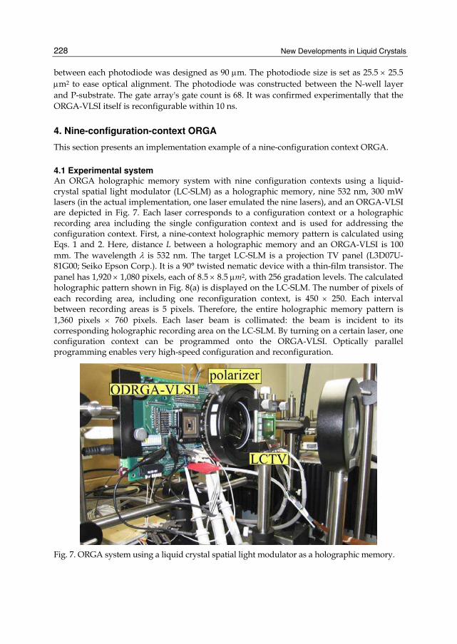
4.1 Experimental system An ORGA holographic memory system with nine configuration contexts using a liquid-crystal spatial light modulator (LC-SLM) as a holographic memory, nine 532 nm, 300 mW lasers (in the actual implementation, one laser emulated the nine lasers), and an ORGA-VLSI are depicted in Fig. 7. Each laser corresponds to a configuration context or a holographic recording area including the single configuration context and is used for addressing the configuration context. First, a nine-context holographic memory pattern is calculated using Eqs. 1 and 2. Here, distance L between a holographic memory and an ORGA-VLSI is 100
mm. The wavelength λ is 532 nm. The target LC-SLM is a projection TV panel (L3D07U-81G00; Seiko Epson Corp.). It is a 90° twisted nematic device with a thin-film transistor. The
panel has 1,920 × 1,080 pixels, each of 8.5 × 8.5 μm2, with 256 gradation levels. The calculated holographic pattern shown in Fig. 8(a) is displayed on the LC-SLM. The number of pixels of
each recording area, including one reconfiguration context, is 450 × 250. Each interval between recording areas is 5 pixels. Therefore, the entire holographic memory pattern is
1,360 pixels × 760 pixels. Each laser beam is collimated: the beam is incident to its corresponding holographic recording area on the LC-SLM. By turning on a certain laser, one configuration context can be programmed onto the ORGA-VLSI. Optically parallel programming enables very high-speed configuration and reconfiguration.
Fig. 7. ORGA system using a liquid crystal spatial light modulator as a holographic memory.
Optoelectronic Device using a Liquid Crystal Holographic Memory
229
(a)
(b) (c)
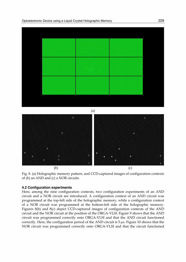
Fig. 8. (a) Holographic memory pattern, and CCD-captured images of configuration contexts of (b) an AND and (c) a NOR circuits.
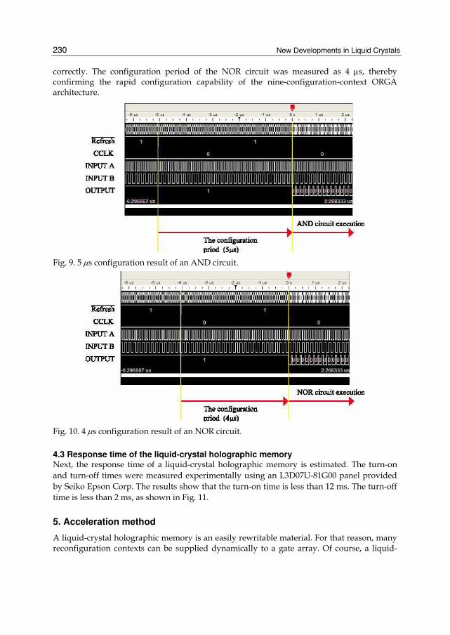
4.2 Configuration experiments Here, among the nine configuration contexts, two configuration experiments of an AND circuit and a NOR circuit are introduced. A configuration context of an AND circuit was programmed at the top-left side of the holographic memory, while a configuration context of a NOR circuit was programmed at the bottom-left side of the holographic memory. Figures 8(b) and 8(c) depict CCD-captured images of configuration contexts of the AND circuit and the NOR circuit at the position of the ORGA-VLSI. Figure 9 shows that the AND circuit was programmed correctly onto ORGA-VLSI and that the AND circuit functioned
correctly. Here, the configuration period of the AND circuit is 5 μs. Figure 10 shows that the NOR circuit was programmed correctly onto ORGA-VLSI and that the circuit functioned
New Developments in Liquid Crystals
230
correctly. The configuration period of the NOR circuit was measured as 4 μs, thereby confirming the rapid configuration capability of the nine-configuration-context ORGA architecture.
Fig. 9. 5 μs configuration result of an AND circuit.
Fig. 10. 4 μs configuration result of an NOR circuit.
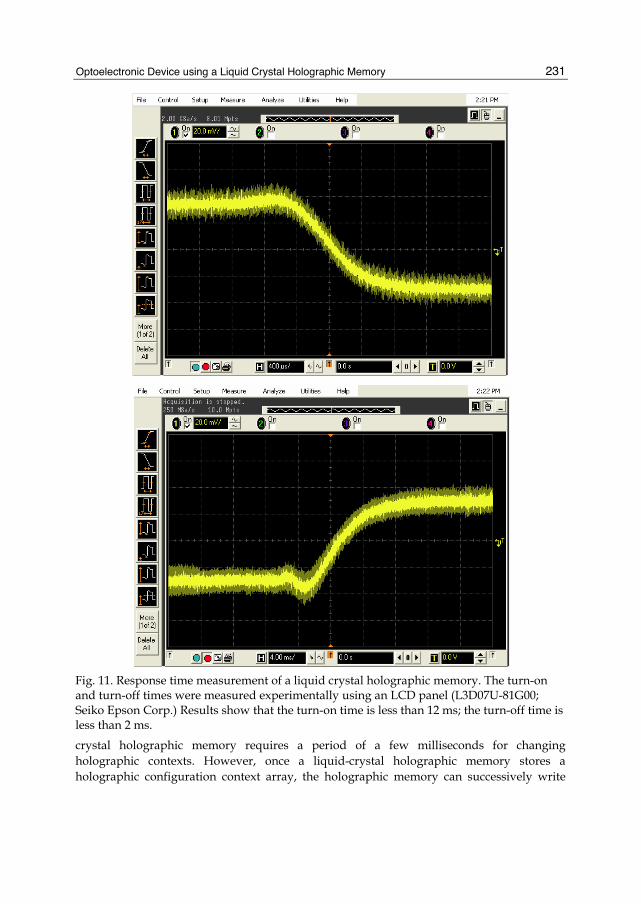
4.3 Response time of the liquid-crystal holographic memory Next, the response time of a liquid-crystal holographic memory is estimated. The turn-on
and turn-off times were measured experimentally using an L3D07U-81G00 panel provided
by Seiko Epson Corp. The results show that the turn-on time is less than 12 ms. The turn-off
time is less than 2 ms, as shown in Fig. 11.
5. Acceleration method
A liquid-crystal holographic memory is an easily rewritable material. For that reason, many reconfiguration contexts can be supplied dynamically to a gate array. Of course, a liquid-
Optoelectronic Device using a Liquid Crystal Holographic Memory
231
Fig. 11. Response time measurement of a liquid crystal holographic memory. The turn-on and turn-off times were measured experimentally using an LCD panel (L3D07U-81G00; Seiko Epson Corp.) Results show that the turn-on time is less than 12 ms; the turn-off time is less than 2 ms.
crystal holographic memory requires a period of a few milliseconds for changing
holographic contexts. However, once a liquid-crystal holographic memory stores a
holographic configuration context array, the holographic memory can successively write
New Developments in Liquid Crystals
232
configuration contexts of the holographic configuration context array onto the gate array.
Consequently, although a context preparation for a liquid-crystal holographic memory takes
a long time, once it is completed, rapid configurations can be done easily. The average
configuration time becomes the value of the response time of the liquid-crystal holographic
memory divided by the array number of holographic configuration context array if it is
assumed that the laser reconfiguration period is negligible compared to the response time of
a liquid-crystal holographic memory. Therefore, when each configuration time TConf. is much
smaller than the switching time TLC of a liquid-crystal holographic memory, the equation is
estimated as the following.
.LCVirtualcycle
TT
N0 (13)
As configuration contexts become more numerous in the future, this architecture is expected
to become increasingly useful.
6. Conclusion
This chapter has described an optically reconfigurable gate array (ORGA) with an LC-SLM
and a reconfiguration-speed acceleration method. The ORGA architecture has enabled the
achievement of microsecond-order reconfiguration and nine configuration contexts.
Although the LC-SLM response time is not faster than that of silicon devices, the use of
multiple configurations decreases the average configuration period. Based on that
improvement, this easily programmable LC-SLM was demonstrated as useful for ORGA
applications.
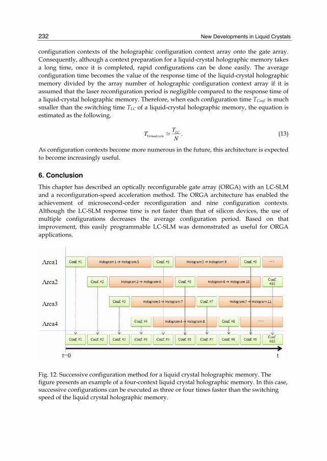
Fig. 12. Successive configuration method for a liquid crystal holographic memory. The figure presents an example of a four-context liquid crystal holographic memory. In this case, successive configurations can be executed as three or four times faster than the switching speed of the liquid crystal holographic memory.
Optoelectronic Device using a Liquid Crystal Holographic Memory
233
7. Acknowledgments
This research was supported by the Ministry of Education, Science, Sports and Culture, Grant-in-Aid for Scientific Research on Innovative Areas, No. 20200027. The VLSI chip in this study was fabricated in the chip fabrication program of VLSI Design and Education Center (VDEC), the University of Tokyo in collaboration with Rohm Co. Ltd. and Toppan Printing Co. Ltd. Also, some experiments were supported by Mr. M. Nakajima and Mr. T. Mabuchi.
8. References
[1] Takuya Otani, "Seiko Epson Develops New Liquid Crystal Panel for Rear Projection TV," Nikkei Electronics, 2006.
[2] SEIKO EPSON CORPORATION, "Epson Develops Next-Generation HTPS Panel for LCD Projection TVs," News Release, 2006.
[3] Sony Corporation, "Sony develops "SXRD", a display device capable of generating high resolution, high contrast images of film quality smoothness," Press Releases, 2003.
[4] Canon Incorporated, "CANON ANNOUNCES DEVELOPMENT OF OWN LCOS REFLECTIVE LCD PANEL," Press Release, 2008.
[5] J. Mumbru, G. Panotopoulos, D. Psaltis, X. An, F. Mok, S. Ay, S. Barna, E. Fossum, "Optically Programmable Gate Array," SPIE of Optics in Computing 2000, Vol. 4089, pp. 763-771, 2000.
[6] J. Mumbru, G. Zhou, X. An, W. Liu, G. Panotopoulos, F. Mok, and D. Psaltis, "Optical memory for computing and information processing," SPIE on Algorithms, Devices, and Systems for Optical Information Processing III, Vol. 3804, pp. 14-24, 1999.
[7] J. Mumbru, G. Zhou, S. Ay, X. An, G. Panotopoulos, F. Mok, and D. Psaltis, "Optically Reconfigurable Processors," SPIE Critical Review 1999 Euro-American Workshop on Optoelectronic Information Processing, Vol. 74, pp. 265-288, 1999.
[8] Altera Corporation, "Altera Devices," http://www. altera.com. [9] Xilinx Inc., "Xilinx Product Data Sheets," http://www. xilinx.com. [10] Lattice Semiconductor Corporation, "LatticeECP and EC Family Data Sheet,"
http://www. latticesemi.co.jp/products, 2005. [11] M. Watanabe, F. Kobayashi, "Dynamic Optically Reconfigurable Gate Array," Japanese
Journal of Applied Physics, Vol. 45, No. 4B, pp. 3510-3515, 2006. [12] M. Miyano, M. Watanabe, F. Kobayashi, "Optically Differential Reconfigurable Gate
Array," Electronics and Computers in Japan, Part II, Issue 11, vol. 90, pp. 132-139, 2007.
[13] N. Yamaguchi, M. Watanabe, "Liquid crystal holographic configurations for ORGAs," Applied Optics, Vol. 47, No. 28, pp. 4692-4700, 2008.
[14] D. Seto, M. Watanabe, "A dynamic optically reconfigurable gate array - perfect emulation," IEEE Journal of Quantum Electronics, Vol. 44, Issue 5, pp. 493-500, 2008.
[15] http://www.ipflex.co.jp [16] H. Nakano, T. Shindo, T. Kazami, M. Motomura, "Development of dynamically
reconfigurable processor LSI," NEC Tech. J. (Japan), vol. 56, no. 4, pp. 99-102, 2003.
New Developments in Liquid Crystals
234
[17] A. Dehon, "Dynamically Programmable Gate Arrays: A Step Toward Increased Computational Density," Fourth Canadian Workshop on Field Programmable Devices, pp. 47-54, 1996.
[18] S.M.Scalera and J.R.Vazquez, "The design and implementation of a context switching FPGA," IEEE symposium on FPGAs for Custom Computing Machines, pp. 78-85, 1998.
[19] S.Trimberger, et al. "A Time--Multiplexed FPGA," FCCM, pp. 22-28, 1997. [20] D. Jones, D.M.Lewis, "A time--multiplexed FPGA architecture for logic emulation,"
Custom Integrated Circuits Conference, pp. 495 - 498, 1995. [21] M. Nakajima, M. Watanabe, "Fast reconfiguration experiments of an optically
differential reconfigurable gate array with 9 configuration contexts, IEEE International Symposium on Circuits and Systems, pp. 2013-2016, 2009.
[22] M. Nakajima, M. Watanabe, "Fast optical reconfigurations of a nine-context DORGA," International Workshop on Applied Reconfigurable Computing, Vol. 5453, pp. 123-132, 2009.
[23] T. Mabuchi, M. Watanabe, "A 9-context Optically Reconfigurable Gate Array," International SoC Design Conference, pp. 1-4, 2008.
New Developments in Liquid CrystalsEdited by Georgiy V Tkachenko
ISBN 978-953-307-015-5Hard cover, 234 pagesPublisher InTechPublished online 01, November, 2009Published in print edition November, 2009
InTech EuropeUniversity Campus STeP Ri Slavka Krautzeka 83/A 51000 Rijeka, Croatia Phone: +385 (51) 770 447 Fax: +385 (51) 686 166www.intechopen.com
InTech ChinaUnit 405, Office Block, Hotel Equatorial Shanghai No.65, Yan An Road (West), Shanghai, 200040, China
Phone: +86-21-62489820 Fax: +86-21-62489821
Liquid crystal technology is a subject of many advanced areas of science and engineering. It is commonlyassociated with liquid crystal displays applied in calculators, watches, mobile phones, digital cameras, monitorsetc. But nowadays liquid crystals find more and more use in photonics, telecommunications, medicine andother fields. The goal of this book is to show the increasing importance of liquid crystals in industrial andscientific applications and inspire future research and engineering ideas in students, young researchers andpractitioners.
How to referenceIn order to correctly reference this scholarly work, feel free to copy and paste the following:
Minoru Watanabe (2009). Optoelectronic Device using a Liquid Crystal Holographic Memory, NewDevelopments in Liquid Crystals, Georgiy V Tkachenko (Ed.), ISBN: 978-953-307-015-5, InTech, Availablefrom: http://www.intechopen.com/books/new-developments-in-liquid-crystals/optoelectronic-device-using-a-liquid-crystal-holographic-memory