Embed Size (px)
Citation preview

0
Opto-Electronic Study of SiC Polytypes:Simulation with Semi-Empirical
Tight-Binding Approach
Amel Laref1 and Slimane Laref2
1Department of Physics and Astronomy, King Saud University,Riyadh 11451, Saudi Arabia
and Department of physics, National Taiwan University, Taipei 1062Université de Lyon, CNRS, Ecole Normale Supérieure de Lyon, Institut de Chimie de
Lyon, Laboratoire de Chimie, Lyon1Taiwan2France
1. Introduction
The recent growing scientific and technological interest on silicon carbide (SiC) arises fromits peculiar physical properties, i.e., its mechanical, and chemical stability. Moreover, SiCis considered to be a promising material for electronic and optical devices. Microelectronicdevices made of SiC can be used in high-power, high-speed, high temperature,high-frequency, and even hard-radiation application (1)-(4). The strong bonding betweenSi and C atoms in SiC makes this material very resistant to high temperature and radiationdamage. In view of this extraordinary application potential a thorough knowledge of thestructural and electronic properties of SiC is a matter of both ionic interest and technologicalimportance. In addition to its traditional use as an abrasive (carborundum) there is currentlymuch interest in materials made from SiC fibres, which compare well with their carbon fibrecounterparts. Over a two hundred chemically stable semiconducting polytypes of SiC exist,they have a high bulk modulus and generally wide band gap. From such difference instacking order it is possible to get almost 200 different crystal structures (1)-(10) of whichthe two extremes are the pure cubic polytype (with zinc blende structure) and the purehexagonal one (with wurtzite structure). SiC is the most prominent of a family of close packedmaterials which exhibit a one dimensional polymorphism called polytypism. In addition,numerous hexagonal and rhombohedral structures (11)-(19) of SiC have been identified inaddition to the common cubic form. In fact, SiC is one of the few compounds which formmany stable and long-range ordered modifications, so-called polytypes (11)-(17). Previously,SiC has been subject to many theoretical studies. With this respect, a variety of structural,electronic and optical properties in SiC have been investigated by many theoretical groups(12)-(15) and the results can be related to the experimental works (7)-(10). In the last years,first-principle calculations have been applied to determine the ground-state properties ofcubic and hexagonal polytypes of SiC (19)-(53). Based on previous theoretical works, thehigh-pressure behavior (18)-(33), and the effect of atomic relaxation on structural properties
16
www.intechopen.com

2 Silicon carbide
were also investigated (14)-(18). Some attempts towards the explanation of the existenceof a large number of metastable SiC polytypes have been also undertaken (14)-(37). Theelectronic band structures of some SiC polytypes have been calculated by several groups(14)-(47). Further studies went deep into the optical properties of SiC polytypes (14)-(33). Theoptical and spectroscopic properties of SiC polymorphs have also been investigated by manygroups both experimentally (7)-(14) and theoretically (19)-(25). Due to the problem of sampleavailability, most measurements were on 6H-SiC and 3C-SiC (54)-(57). Very recently, somemeasurements on 4H-SiC have also been reported (58)-(61). There are considerable variationsin the measured optical properties mainly because the photon energy is limited to less than6.6 eV using the popular ellipsometry technique. The use of vacuum-ultraviolet (VUV)spectroscopy can extend the energy range significantly and so far has only been carried out on6H-SiC (57). Recent advances in crystal growth of SiC have allowed the study of the opticalproperties of different polytypes (54)-(60). In addition, tight-binding (TB) method has provento be very useful for the study of both semiconductors and metallic systems, especially insystems which are too large to be studying via ab-initio techniques. This method is about 2 or3 orders of magnitude faster than the ab initio formulations, and at the same time it describeswith suitable accuracy the electronic structure of the systems. The computational efficiency ofthe TB method derives from the fact that the Hamiltonian can be parametrized. Furthermore,the electronic structure information can be easily extracted from the TB hamiltonian, which,in addition, also contains the effects of angular forces in a natural way. In order to use a morerealistic method, we present a TB model with sp3s* basis, representing exact curvatures oflowest conduction bands. The TB approach is standard and widely used for the electronicproperties of a wide variety of materials. In the present contribution we overview ourmost recent results on the electronic structures and optical properties of SiC polytypes(62). Hence, the SiC polytypes can be considered as natural superlattices, in which thesuccessive layers consist of Hexagonal SiC material of possibly different width. Our TBmodel can treat SiC polytypes as superlattices consisting hexagonal bulk-like blocks. Wehave investigated to which extent it is acceptable approximation for existing polytypes whenvarious of nH-SiC crystal are used to present polytype superlattices. Indeed, this is anaccurate approximation by building blocks consist of n-layers of nH-SiC. By representingin general the polytypes as superlattices, we have applied our recent TB model (62) thatcan treat the dimensions of the superlattice. Within this model we take for each sublayerlinear combination of atomic orbitals of hexagonal SiC which are subsequently matched at theinterfaces to similar combinations in the adjacent sublayers by using the boundary conditions.Polytypic superlattices, in comparison with heterostructure superlattices, have two importantadditional features, namely (i) the polytypes are perfectly lattice-matched superlattices and (ii)the polytypes have an energy band offset between adjacent layers equal to zero by definition.We can obtain with our TB model the band structures and particularly the energy band gapsof SiC polytypes and their wave functions. Our recent TB model (62) is very efficient whenextended it to investigate the electronic properties of wurtzite (wz) superlattices in (0001)direction.This chapter is organized as follows: Section 1 provides a review for the large band-gap SiCbased semiconductor device technology. In the next section we present the different polytismof SiC. A fundamental concept of the TB theory for SiC polytypes is described in section 3.Our recent TB model is specifically applied to study the electronic and optical properties ofSiC polytypes and it can be applied to nH-SiC wurtzite superlattices. The present approachis also suited for all wurtzite semiconductor superlattices and large complex unit cells which
390 Silicon Carbide – Materials, Processing and Applications in Electronic Devices
www.intechopen.com

Opto-Electronic Study of SiC Polytypes: Simulation with Semi-Empirical Tight-Binding Approach 3
can be treated where the transferability of the hopping parameters is required. Section 4 dealswith some of our recent results of the electronic and optical properties of SiC polytypes. Toreach these, we analyzed this statement in terms of optoelectronic properties of SiC polytypes.Finally in section 5 we summarize and conclude.
2. A review of the large band-gap SiC based semiconductor device technology
The recent surge of activity in wide band-gap semiconductors has arisen from the need forelectronic devices capable of operation at high power levels, and high-radiation resistance,and separately, a need for optical materials, especially emitters, which are active in theblue and ultraviolet (UV) wavelengths (63)-(69). In this aspect, there has been renewedinterest in SiC as one of the wide band gap compounds with great potential for the nextgeneration of electronic devices operating at high temperature (61)-(68). This compoundhas been also used primarily in light-emitting diodes. SiC’s intrinsic material propertiesas well as its existence in various polytypes have led to a revival of technological interest.Crystal growth of SiC polytypes has recently shown considerable progress, the expectationnow being that the manufacturing of different electronic devices becomes feasible. The wideband-gap semiconductor SiC, with its excellent thermal conductivity, large breakdown fields,and resistance to chemical attack, will be the material of choice for these applications. Realizedprototype power devices of SiC, like rectifier diodes, and junction field-effect transistors,show indeed encouraging performance results under extreme conditions (54)-(66). In theoptical device arena, the ever increasing need for higher density optical storage and fullcolor display technologies are driving researchers to develop wide band-gap semiconductoremitting technologies which are capable of shorter wavelength operation. Since the differentenergy gap values of SiC all happen to lie in the visible range of the spectrum, SiC is aninteresting optical device material. Indeed, blue light emitting diodes were the first electronicSiC devices which found a good sale. Some SiC polytypes are in addition most promisingas photodetective material sensitive to ultraviolet radiation. SiC is a good candidate for ashort wave length diode laser. Prototype transistors have been fabricated from SiC, and themicrowave and high temperature performance of SiC transistors have been studied. Deviceslike field effect transistors, bipolar storage capacitors, and ultraviolet detectors have beenfabricated (57)-(64). SiC has a relatively high atomic bonding energy which is responsible forits mechanical strength and chemical stability at high temperatures. This material can withoutmajor difficulty, be crystallized in several polytypes, primarily due to similar geometricstructures and atomic bonds (1)-(11). The different stacking of C-Si bilayers remarkablyinfluences the properties of SiC. The most pronounced example concerns their electronicstructure. Hence, a controlled epitaxial growth of different polytypes on each other wouldlead to high-quality heterostructures of chemical identical material with a locally adjustableband gap (7)-(14). Meanwhile, growth of heterocrystalline structures seems to be possible (4),but exhibits problems with the reproducibility and the crystal quality. Another possibilityto create a combination of two polytypes is a solid-solid phase transition, which transformsone polytype into another one (6)-(8). However, polytypism also gives some advantages forconstructing electronic devices, for example homo-material heterostructures. Quantum wellscan be made by embedding a SiC polytype in another polytype with a wider gap(55)-(60).Among the SiC polytypes, 6H is most easily prepared and best studied, while the 3C and4H polytypes are attracting more attention for their superior electronic properties. The verysimple structure 2H is, in fact, very rarely produced by the employed growth techniques.Already, commercial applications have been done but most of the developments in industry
391Opto-Electronic Study of SiC Polytypes: Simulation with Semi-Empirical Tight-Binding Approach
www.intechopen.com

4 Silicon carbide
Fig. 1. (a) HRTEM image, displaying that the 3C/6H-SiC polytipic transformation takesplace by three bilayers thin lamellae twinned along the (111) planes and bounded along the(112) planes. Image (b) presents a magnification of the area marked by the square in (a) (56).
and research laboratories focus on two hexagonal polytypes : the 6H and 4H-SiC varieties. Thepolytypism of SiC makes it non-trivial to grow single phase material, but it also offers somepotential advantages if crystal growth methods can be developed sufficiently to capitalize onthe possibility of polytype homo/heterojunctions (see figure 1).
2.1 Polytypism in SiC
SiC is a wide band gap semiconductor that can be synthesized in a variety of polytypes:polytypism, can be considered as a one dimensional variant of polymorphism (1)-(8). Indeed,while the term polymorphism generally refers to the possibility of an element or compoundto crystallize in different structures, polytypes only differ for the stacking sequence of atomiclayers along one crystalline direction. We include SiC in the group of polytypes because of itssimplicity and the fact that its hexagonality is 100%. All various SiC-polytypes have the samestoichiometry and the same bonding configuration between next nearest neigbors. More than200 polytypes of SiC exhibiting a wide range of properties have been reported (1). There area lot of more complex polytypes in which the bonding arrangement (cubic vs. hexagonal) arerepeated periodically. Due to that periodic repetition the SiC-polytypes are also called to benatural superlattices. However, only few of those polytypes are commonly found and thoseare relatively simple compared to the rest. The bandgaps differ widely among the polytypesranging from 2.3 eV for 3C-SiC to 2.9 eV in 6H SiC to 3.3 eV for 2H SiC. In general, the greaterthe wurtzite component, the larger the bandgap.A shorthand has been developed to catalogue the literally infinite number of possible polytypecrystal structure. In this notation the number of layers in the stacking direction, before thesequence is repeated, is combined with the letter representing the Bravais lattice type: cubic
392 Silicon Carbide – Materials, Processing and Applications in Electronic Devices
www.intechopen.com

Opto-Electronic Study of SiC Polytypes: Simulation with Semi-Empirical Tight-Binding Approach 5
Fig. 2. Three-dimensional perspective views of the primitive hexagonal unit cells of the3C-(zinc-blende), 2H-(wurtzite), 4H-, 6H-, and 8H-SiC polytypes. The stacking sequencesABC (3C), AB (2H), ABCB (4H), ABCACB (6H) and ABCAB ACB (8H) are also indicated.
(C) or hexagonal (H). With reference to figure 2, if the first Si-C layer is labelled A, the nextlayer that can be placed according to a closed packed structure will be placed either on B orC. The different polytypes are constructed by permutations of these three positions. In figure2 the stacking sequence is shown for the most common polytypes, 3C, 2H, 4H, 6H, and 8H,which are very interesting for their technological applications. Three-dimensional perspectiveviews of the primitive hexagonal unit cells of the 2H-, 3C-, 4H-, 6H-, and 8H-SiC polytypes. Inthe case of SiC, the basic units are tetrahedrons with a C(Si) atom at the center, surrounded byfour Si(C) atoms covalently bonded: these units are periodically repeated in closed-packedhexagonal layers, whose stacking sequence gives rise to the different polytypes. Thoughbeing different in the long range order, the several polytypes show a similar local chemicalenvironment for both the carbon and silicon species; in particular each Si(C) atom is situatedabove the center of a triangle of C(Si) atoms and underneath a C(Si) atom belonging to the nextlayer in a tetrahedral coordination. The SiC-polytypes consist of double silicon-carbon layerswhich are stacked on top of each other in the c-axis direction. A local arrangement of threeconsecutive double layers is called hexagonal, if it is like the arrangement of double layersin wurzite. It is called cubic, if the stacking arrangement is the same as for the zinc-blendestructure. The basic structural elements is the SiC bilayer composed of one Si [0001] plane andthe adjacent C[0001] plane. The SiC polytypes are differentiated by the stacking sequence ofthe tetrahedrally bonded SiC bilayers, such that the individual bond lengths and local atomicenvironments are nearly identical, while the overall symmetry of the crystal is determined bythe stacking periodicity. Each SiC bilayer, while maintaining the tetrahedral bonding schemeof the crystal, can be situated in one of three possible positions with respect to the lattice.These are each arbitrarily assigned the notation A, B, or C. Depending on the stacking order,the bonding between Si and C atoms in adjacent bilayer planes is either of a zincblende (cubic)or wurtzite (hexagonal) nature. Zincblende bonds are rotated 60 with respect to nearestneighbors while hexagonal bonds are mirror images (Figure 2). Each type of bond provides aslightly altered atomic environment making some lattice sites inequivalent in polytypes withmixed bonding schemes and reducing the overall symmetry. These effects are importantwhen considering the substitutional incorporation and electronic transport properties of
393Opto-Electronic Study of SiC Polytypes: Simulation with Semi-Empirical Tight-Binding Approach
www.intechopen.com

6 Silicon carbide
SiC. If the stacking is ABCABC..., the purely cubic, i.e., a zinc-blende structure consistingof two interpenetrating face-centered (fcc) cubic lattices. Zincblende structure commonlyabbreviated as 3C SiC (or β-SiC) is realized (Figure 2). 3C SiC is the only possible cubicpolytype. The stacking direction of the basal planes perpendicular to the planes is in fact [111]direction of the cubic unit cell of 3C-SiC as indicated in the figure. The family of hexagonalpolytypes is collectively referred to as alpha SiC. The purely wurtzite ABAB... stackingsequence is denoted as 2H SiC reflecting its two bilayer stacking periodicity and hexagonalsymmetry. All of the other polytypes are mixtures of the fundamental zincblende and wurtzitebonds. Some common hexagonal polytypes with more complex stacking sequences are 4H-,6H- and 8H- SiC (Figure 2). Since the SiC polytypes are mixtures of cubic and hexagonalstackings, a quantity defined as the hexagonality H representing the fraction of hexagonalstackings out of all the stackings (cubic + hexagonal) in a polytype is used frequently todescribe how much the polytype is cubic-like or hexagonal-like in structural sense [5]. Asit is obvious from the definition, the hexagonality of 2H-SiC is 100 % and that of 3C-SiC is 0%. It is naturally expected that a polytype with a smaller H should be closer to 3C, i.e., morecubic-like than one with a larger H in other material properties as well as in structure, andthis is generally true for most of the polytypes. 4H−, 8H−SiC are composed equally of cubicand hexagonal bonds, while 6H−SiC is two-thirds cubic. Despite the cubic elements, each hasoverall hexagonal symmetry. All these polytypes have higher periodicity (more Si-C bilayers)along the c-axis than 2H-SiC and they are in general called α-SiC together with 2H-SiC. 4H-and 6H-SiC are the most common polytypes, and single crystal wafers of these polytypes arecurrently available and hence all recent research for making commercial devices out of SiC arefocused on these polytypes.
3. Empirical tight-binding model for hexagonal and n-hexagonal systems: General
formalism of the tight-binding model for (0001) wurtzite:
The tight-binding approximation for band structure calculations uses atomic energyparameters and the expansion of the electron wave functions in terms of a linear combinationof atomic orbitals (LCAO). In the LCAO method, the basic problem is to find the Hamiltonianmatrix elements between the various basis states, as in the original paper of Slater andKoster (70); the matrix elements can be written for the basis functions sp3 consideringvarious possible interactions. In our recent calculations, a standard semi-empirical sp3s*tight-binding method (71) has been employed and the matrix elements are parametrized inorder to reproduce the principal features to know the band structures.The general form of the Hamiltonian is (72).
H (k) = ∑bb′ ,l
∑αβ
eik.Rlbb′ Ebb′
αβ
(
Rlbb′
)
(1)
where l labels the sublayers, b and b′ refer to the atomic basis within a sublayer, and α and β
are atomiclike orbitals. Given the Ebb′αβ ’s (bulk band structure) and the R
lbb′ ’s (SL geometry),
we can construct the Hamiltonian matrix and diagonalize it directly for the eigensolutions.In our recent study, we have performed a TB method with an sp3s∗ basis set (71). We used thenearest-neighbor TB parameters with a basis of five orbitals (s, px, py, pz, and s*) per atom.We have derived a TB Hamiltonian pH (p = 2, 4, 6, 8,..) for different polytypes of SiC fromthe wz TB model. The label pH (p = 2, 4, 6, 8,..) is the hexagonality for different polytypes.Consider a TB Hamiltonian of two different alternating wz crystals labelled ”ca” in (0001)
394 Silicon Carbide – Materials, Processing and Applications in Electronic Devices
www.intechopen.com

Opto-Electronic Study of SiC Polytypes: Simulation with Semi-Empirical Tight-Binding Approach 7
direction, where c and a are labelled cation and anion atoms. The pH (p = 2, 4, 6, 8,..) contains2(2n) atoms in a unit cell at Ri with five orbitals each; |αj >, where α denotes the s, x(= px),y(= py), z(= pz) and s∗(=excited s) orbitals, and j represents the site index in a unit cellwhich runs from 1 through 2(2n).For each wave vector k in the Brillouin zone (BZ), the Bloch functions can be constructed bythe linear combination of atomic orbitals |ξ, rα, Rl > :
|ξ, rα, k >=1√N
∑l
eik.Rl+ik.rα |ξ, rα, Rl > (2)
Here ξ is a quantum number that runs over the basis orbitals s, s*, px, py, and pz on thedifferent types of sites α in a unit cell. The N wave vectors k lie in the first BZ with the originof the lth unit cell at Rl , and rα represents the positions of the atoms in this unit cell.The electronic eigen-states of the pH (p = 2, 4, 6, 8,..) are expanded as :
|k, λ > = ∑ξ,α
< ξ, rα, k|k, λ > |ξ, rα, k > (3)
= ∑ξ,α
Cξα (k, λ) |ξ, rα, k >
λ denotes the band index and Cξα (k, λ) is the eigen-wavefunction, which can be obtained bysolving the Schrödinger equation.
∑ξ,α′
[⟨
ξ, rα, k|H|ξ ′, rα′ , k⟩
− Eλ (k) δξξ ′δαα′]
< ξ, rα, k|k, λ >= 0 (4)
Therefore, we obtain the Hamiltonian matrix for pH (p = 2, 4, 6, 8,..).
1 2 3 . . n − 1 n 1 2 3 . . n (5)
H =
1234
n − 1n12.n − 1n
⎡
⎢
⎢
⎢
⎢
⎢
⎢
⎢
⎢
⎢
⎢
⎢
⎢
⎢
⎢
⎢
⎢
⎢
⎢
⎢
⎢
⎢
⎢
⎣
Ha Hac H+0 ca
Hc H0acHa
Hc.
..
HaHc H0ac
Ha HacHc H0ac
. .Ha Hac
Hc
⎤
⎥
⎥
⎥
⎥
⎥
⎥
⎥
⎥
⎥
⎥
⎥
⎥
⎥
⎥
⎥
⎥
⎥
⎥
⎥
⎥
⎥
⎥
⎦
Here, the blocks Hc(a), Hac, and H0ac denote intra-material interactions for pH (p = 2, 4, 6, 8,..),and every element represents a 5x5 matrix. The blocks Hca and H0ca are expressed as:
Hac =
[
a acac+ c
]
, H0ac =
[
aa acca cc
]
(6)
395Opto-Electronic Study of SiC Polytypes: Simulation with Semi-Empirical Tight-Binding Approach
www.intechopen.com

8 Silicon carbide
Fig. 3. Brillouin zones of (a) cubic (b) hexagonal structures.
The diagonal elements H(j = a, and c) correspond to intra-site energies, and the otherscontain the nearest atomic interactions in the same layer (Hij) or between two neighborlayers (H0ij) perpendicular to the (0001) direction. The terms a and c are regarded asthe anion and cation atoms of the SiC semiconductor. The intra-material elements in theHamiltonian can be formed uniquely by using the corresponding bulk parameters. Our TBparameters (62) give the correct indirect and direct gap in comparison with Ref.(73) and arechecked for their transferability to all considered structures by calculating the optoelectronicproperties of different polytypes of SiC. This method reduces the size of the Hamiltonianmatrix considerably compared with methods based on plane-wave basis and allows us totreat localized states. Our TB Hamiltonian can be generalized to the wz based SL’s in (0001)direction with two different compounds and is efficient when extended it to investigate theelectronic properties of wz SL’s. Then, we present some of our recent results which we haveobtained by our TB model for electronic and optical properties of SiC polytypes.
4. Electronic and optical properties of polytypic SiC
We start this section with some of our recent results for SiC polytypes in order to illustrate theelectronic and optical properties of this system. With a TB scheme, the detailed calculations ofelectronic structure and optical properties of different polytypes of SiC are presented.
4.1 Electronic band structures of 3C-, 2H-, 4H-, 6H-, and 8H-SiC:
A very important aspect of the polytypism of SiC is the change in energy band structure, andhow it does appear in the different polytypes. Having established the geometric structurefor the polytypes, the electronic band structure was calculated along the symmetry directions(62). Figure 3 shows the BZs of cubic, and hexagonal polytypes with high symmetry pointsmarked. The labeling of the symmetry points and the three symmetry lines out from the Γ
point in the relevant hexagonal Bzs are shown in Figure 3.The corresponding band structure of 3C-SiC is shown in figure 4. The conduction bandminimum (CBM) for 3C-SiC is lying at the X point and the number of CBMs equals tothree (2). The resulting TB band structures of SiC polytypes (2H, 4H, 6H, and 8H) are alsorepresented in Figure 4 versus high-symmetry lines A-L-M-Γ-A-H-K-Γ. For all polytypes thegap is systematically identified as an indirect one. The valence band maximum is located for
396 Silicon Carbide – Materials, Processing and Applications in Electronic Devices
www.intechopen.com

Opto-Electronic Study of SiC Polytypes: Simulation with Semi-Empirical Tight-Binding Approach 9
all polytypes at the centre of the BZ. The valence band maximum (VBM) is found to be at thecenter of the BZ at Γ point for all polytypes. The zero energy is used for all polytypes. Inthe case of 2H-SiC, the CBM is at the K point with two equivalent CBMs (73), (74), (75), (77),while 4HSiC has its CBM at the M point giving three equivalent CBMs (22), (25),(76), (78),(79)[Figure 4]. For 6H-SiC, the theoretical calculations predict the conduction band supplying theglobal CBM to be very flat along the ML line and the CBM resides at some place on the line,resulting in six equivalent CBMs (22), (25), (78),(79). This has been confirmed experimentallyfrom the Raman scattering measurement by Colwell et al. (80). However, the exact location ofthe CBM and the detailed shape of conduction band affecting the determination of effectiveelectron mass are not yet well-established, either experimentally or theoretically. There aresimilarities between the band structures of the hexagonal polytypes, both in the valenceand the conduction bands, especially between 4H, 6H and 8H-SiC structures. A significantdifference between 2H and the other three hexagonal polytyes is that in 2H-SiC the two lowestconduction bands have an intersection along MK line and that the lowest band at K point hasa one-dimensional representation (in the single group representation). Both in 4H, 6H and8H-SiC the two lowest conduction bands at K point are degenerate. The intersection in 2H-SiCmakes it possible for the second lowest band at the M point to provide a global conductionband minimum at the K point with C3v symmetry whereas the minimum for 4H-SiC is atM (C2v) and for 6H-, and 8H-SiC along the ML line (also C2v symmetry), 44 % out from Mtowards L. The variation in band energy gaps is coming from the different locations of CBMs.This is related with the stacking and period of each polytype. Interestingly, it is predictedtheoretically that the offsets of VBMs among different polytypes are quite small, at most0.10-0.13 eV for the case of 2H and 3C (11),(14). In other words, the VBMs of all polytypesare similarly located in energy. This means that the considerable variation of band gap fordifferent polytypes is mainly due to the difference of CBM location.Another interesting point to note in the conduction band structures of SiC polytypes is thelocation of second CBM. According to the calculation done by Persson et al. (26),(38), thesecond CBM of 3C-SiC is at the same symmetry point (X) as the first one with 2.92 eV higherin energy and this was confirmed experimentally from optical absorption measurementswith slightly larger energy difference ( 3.1 eV) between the two minima (13). Persson et al.calculations also show that the three hexagonal polytypes (2H, 4H, 6H) have their secondCBMs located at the M point and the energy difference between the first and second CBMs is0.60 eV for 2H, 0.122 eV for 4H, and 1.16 eV for 6H respectively. The energy position of thesecond CBM in 4H-SiC has been probed experimentally by BEEM (56)-(58) and optical phononspectra measurements (59)-(63), with measured energy that ranges 0.10-0.14 eV above the firstCBM. The band gaps of several common polytypes of SiC have been measured carefully byChoyke et al. from the optical absorption or luminescence spectra of the polytypes (27). Themeasured band gaps range widely from 2.390 eV for 3C-SiC to 3.330 eV for 2H-SiC and lot ofwork has been done to understand all details of the corresponding variations. Those for 4H-and 6H-SiC which are in between the two extreme cases in structure are measured to be 3.265eV and 3.023 eV respectively. So, from fig.4, it is clear that the valence and the conductionbands are well described. Moreover, our results are in good agreement with the experimentalresults (74). All energies are with reference to the top of the valence band. The results showthat SiC is an indirect gap semiconductor. In addition, the calculated energy gaps of SiC arein good agreement with the other results (73), (74), (75), (77).Values of lowest indirect forbidden gaps (Eg) are listed in Table 1 in comparison with theavailable data in the literature and experimental results. Our TB model provides good results
397Opto-Electronic Study of SiC Polytypes: Simulation with Semi-Empirical Tight-Binding Approach
www.intechopen.com

10 Silicon carbide
Fig. 4. Band structures for 3C-, 2H-, 4H-, 6H-, and 8H-SiC calculated by our sp3s* TB model(62).
398 Silicon Carbide – Materials, Processing and Applications in Electronic Devices
www.intechopen.com
Opto-Electronic Study of SiC Polytypes: Simulation with Semi-Empirical Tight-Binding Approach 11
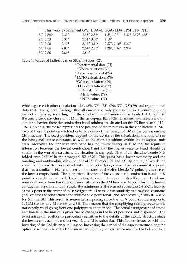
This work Experiement GW LDA+U GGA/LDA EPM ETB NTB
3C 2.389 2.39c 2.38b 2.52d 1.5e, 1.27 f 2.30g 2.47h 1.33i
2H 3.33 3.30a 3.31b 3.33d 2.10 f
4H 3.20 3.19a 3.18b 3.16d 2.57e, 2.18 f 3.20g
6H 2.86 2.85a 2.84b 2.90d 2.28e, 1.96 f 2.99g
8H 2.86 2.86a 2.84b
Table 1. Values of indirect gap of SiC polytypes (62).a Experimental data (75)
bGW calculations (73)c Experimental data(74)
d LMTO calculations (78)eGGA calculations (79)f LDA calculations (25)
g EPM calculations (22)h ETB values (76)i NTB values (77)
which agree with other calculations (22), (25), (73), (75), (76), (77), (78),(79) and experimentaldata (74). The general findings that all considered polytypes are indirect semiconductorsare not surprising, including that the conduction-band minimum is located at X point inthe zinc-blende structure or at M in the hexagonal BZ of 2H. Diamond and silicon show asimilar behavior, there the conduction-band minima are situated on the ΓX line near X [110].The X point in the fcc BZ represents the position of the minimum in the zinc-blende 3C-SiC.Two of these X points are folded onto M points of the hexagonal BZ of the corresponding2H structure. The exact positions depend on the details of the calculations, the ratio c/a ofthe hexagonal lattice constants, as well as the atomic positions within the hexagonal unitcells. Moreover, the upper valence band has the lowest energy in X, so that the repulsiveinteraction between the lowest conduction band and the highest valence band should besmall. In the wurtzite structure, the situation is changed. First of all, the zinc-blende X isfolded onto 2/3LM in the hexagonal BZ of 2H. This point has a lower symmetry and thebonding and antibonding combinations of the C 2s orbital and a Si 3p orbital, of which thestate mainly consists, can interact with more closer lying states. The minimum at K point,that has a similar orbital character as the states at the zinc blende W point, gives rise tothe lowest empty band. The energetical distance of the valence and conduction bands in Kpoint is remarkably reduced. The resulting stronger interaction pushes the conduction-bandminimum away from the valence bands. States on the LM line near M point form the lowestconduction-band minimum. Surely, the minimum in the wurtzite structure 2H-SiC is locatedat the k point in the center of the BZ edge parallel to the c axis similarly to hexagonal diamond(79). We find the conduction band minima at M point for 4H and, respectively, at about 0.63LMfor 6H and 8H. This result is somewhat surprising since the fcc X point should map onto1/3LM for 4H and M for 6H and 8H. That means that the simplifying folding argument isnot exactly valid going from one polytype to another one. The actual arrangement of atomsand bonds in the unit cells gives rise to changes in the band positions and dispersion. Theexact minimum position is particularly sensitive to the details of the atomic structure sincethe lowest conduction band between L and M is rather flat. This flatness increases with thelowering of the LM distance in k space. Increasing the period of the superstructure along theoptical axis (line Γ-A in the BZ) causes band folding, which can be seen for the Γ-A and K-H
399Opto-Electronic Study of SiC Polytypes: Simulation with Semi-Empirical Tight-Binding Approach
www.intechopen.com

12 Silicon carbide
directions for the SiC polytypes shown in Figure 4. The overall features of the band structuresagree well with previous calculations . Differences concern the magnitudes of the variousband gaps, where the effect is related to the variations in the position of the conduction-bandminima. An interesting problem concerns the preparation of heterostructures on the baseof chemically identical, but structural inequivalent semiconductors, more strictly speaking ofdifferent polytypes. The key parameters of such structures are the band offsets at the interface.
4.2 Effective masses of 3C-, 2H-, 4H-, 6H-, and 8H-SiC
The effective electron masses for the different polytypes have been calculated and measuredexperimentally by different scientific groups (19), (22), (26), (81), (82), (83). The valuesvary depending on the experimental techniques or model used, especially for the hexagonalpolytypes. Results for the lowest conduction band minima in K, M points, or at the LMline near M point are calculated (62). For electrons we give the full inverse effective-masstensor along the principal axis determined by the c axis of the structure and the position ofthe minimum in k space. We consider the longitudinal masses m|| parallel to the connectionline between the minimum position and more strictly speaking parallel MΓ(4H), KΓ (2H)and (LM)Γ (6H, 8H). The two transverse masses m⊥1, m⊥2 are distinguished according tothe anisotropy of the system. m⊥ denotes the transverse mass parallel to the c axis. In thecalculation of m⊥1 we use the direction ML. For the estimation of the second transversemass m⊥2 of the hexagonal polytypes we replace the correct direction by the line MK in anapproximate manner.Our previously calculated values of the electron effective masses in three principal directionswith the tight-binding method (62) are presented in table 2 in comparison with othertheoretical and experimental data. All values of the electron effective masses agree withexperimental values, when available, and for 3C-, 2H-, and 4H-SiC, our results agree withthe majority of earlier calculations (22). We report in the same table our values of m∗ for8H-SiC. There is no available experimental data for comparison. No clear trend with thehexagonality or the extent of the unit cell can be derived from table 2 for the electron masses.This is not astonishing since the conduction band minima appear at different k points inthe BZ. Only in 4H case one observes the minimum at the same point M. A remarkableanisotropy of the electron effective mass tensor is found for 6H and 4H. In space directions(nearly) parallel to MΓ and LΓ heavy electrons appear whereas the mass for the electronmotion in the plane perpendicular to c axis but parallel to the edge MK of the hexagonalBZ is small. This is a consequence of the flatness of the lowest conduction bands in themost space directions. The electron-mass anisotropy in the 2H polytypes at M or K is muchsmaller. The findings for the conduction band masses have consequences for the electronmobility, since this property is proportional to the inverse mass. We expect that at least forthe mostly available 6H− and 4H-SiC polytype, the current directions should be carefullyselected. Otherwise, too small electron mobilities result. 2H-SiC have more parabolic behavioraround their minima, whereas in 4H- and 6H-SiC the interaction between the two close-lyingbands at the M point will affect the parabolicity, especially for the flat curvatures in the cdirection. The best agreement between theory and experiment seems to be for the 2H-SiCpure hexagonal polytype and the 3C-SiC cubic polytype. For the 8H-SiC polytype there arenot yet any experimental results for the effective electron masses. Also there is only oneexperimental report for the longitude effective mass of 6H-SiC. For the hole effective massesthere are few theoretical reports of the polytypes and even fewer are the experimental values.The effective electron masses of 3C- and 4H-SiC have been measured experimentally and
400 Silicon Carbide – Materials, Processing and Applications in Electronic Devices
www.intechopen.com

Opto-Electronic Study of SiC Polytypes: Simulation with Semi-Empirical Tight-Binding Approach 13
Mass 3C 2H 4H 6H 8H
m‖ 0.69 0.40 0.60 0.65 0.67
0.667c 0.42a 0.58a 0.68a
0.70b 0.43 f 0.53b 0.44b
0.449d 0.58e 0.77e
0.68 f 0.57 f 0.75 f
m⊥1 0.25 0.24 0.36 1.19 1.380.247c 0.22a 0.33a 1.25a
0.24b 0.26 f 0.31e 1.14b
0.23 f 0.31 f 1.42e
1.83 f
m⊥2 0.25 0.40 0.21 0.10 0.150.247c 0.42a 0.29a 0.13a
0.24b 0.43 f 0.19b 0.43e
0.23 f 0.28e 0.24 f
0.28 f
Table 2. Effective masses of electrons in the conduction-band-minima. All values in units ofthe free-electron mass m0 (62).
a Experimental values (81).b EPM calculations (22).
c Experimental values (82).d LMTO (GW) (83).
e LMTO (19).f FPLAPW (26).
reported by several groups, and they agree quite well with the theoretically calculated values(19), (26), (83). For 6H-SiC, only the longitudinal effective mass along the c-axis has beenmeasured (82), but due to the peculiar band shape along the direction there is still a largeinconsistency between the measured value and the calculated ones, even among the valuescalculated theoretically by different groups (19), (26), (83). However, only the hole effectivemasses of 4H-SiC have been measured experimentally and reported by Son et al. (81).
4.3 Total density of states of 3C-, 2H-, 4H-, 6H-, and 8H-SiC
We have applied the tetrahedron technique directly from the eigenvalues and the angularmomentum character of each state. This is done by dividing up the Brillouin zone into 48tetrahedron cube. The total density of states (TDOS) of 3C-SiC, corresponding to the bandstructure is given in figure 5 (62). The 3C-SiC have valence band density of states qualitativelysimilar to homopolar semiconductors, except for the gap which opens at X point. This gapis related to different potential for the cation and anion potentials. This ”antisymetric” gaphas been proposed as a measure of crystal ionicity. The lowest states contain a low-lying Cs-derived band about 17 eV below the VBM. The lowest states of the VB from -17 to -13 eVhas primarily s character and is localized on the anion. The large peak at -10 to -7 eV comesprimarily from the onset of the second valence band at points X and L. The states of this bandis primarily of cation s character, it changes rapidly to anion p-like at the top of valence band.From the Fig 5, it is apparent that there is a significant amount of Si p hybridization all theway up to the VBM. A comparison with the corresponding DOS curve of the experimental
401Opto-Electronic Study of SiC Polytypes: Simulation with Semi-Empirical Tight-Binding Approach
www.intechopen.com

14 Silicon carbide
results reveals excellent agreement for energies below 4 eV. The bandwidths and energies arein good agreement with photoemission results (74).The DOS was determined by the tetrahedron integration over a mesh that was generated bysix cuts in the Γ-M direction of the BZ and included 112, 84, 78 and 56 points in the irreduciblepart of 2H, 4H, 6H and 8H BZ, respectively. In Figure 5 total densities of states of SiC polytypes(62) are shown which can be used for the interpretation of photoemission spectra of SiC. Thelowest valence band in 6H SiC between -19.0 and -13.0 eV is dominated by s-electrons of Catom. The maximum at 14.85 eV in the total DOS is dominated by the s-electron of Si. Theupper part of the valence band of 6H SiC is dominated mainly by the p-electron of C and Si.The conduction band is mainly dominated by the s, and p-electrons of Si, whereas p-electronsof C are less dominant. There is a noticeable difference of the p-state occupation for differentpolytypes and for different sites in the same polytype. The band width of the valence bandagrees with previous works represented in many literatures [(22), (25), (73), (75), (77), (78)],where 18.0 eV were obtained. Our value of the valence band width (≈19.0 eV) of 6H SiC islower than in cubic SiC as expected (25), (73),(78),(79).In the figure 5, one can see that the valence band, as expected, consists of two subbands.The energy width of these subbands and the total bandwidth are very similar for the fourpolytypes. In α-SiC polytypes the lower-lying subbands is in the range from about -19.5 to-13 eV and is dominated by the atomic Si 3s+3p states and the localized atomic C 2s states,whereas the higher subband also consists of Si 3p and 2p states. In the higher subband theSi 3s and C 2p states dominate at lower energies and the C 2p states dominate at higherenergies. Even if it is not straightforward to compare photoemission spectra with the DOS,the clear peak at about -11.1 eV, arising from the atomic C 2p and Si 3s states, can probably beidentified with the experimental value -10.5 eV (74). Also, the total band-width and the widthof the higher subband seem to be in agreement with experimental results. The calculatedwidth of the total band (higher subband) is about 8.5 eV for all four polytypes, whereas theexperimental results for α-SiC polytypes are about 10.0 eV (74).Since band structures accurate close to the band gap are desired, it is useful to examinethe density of states in this region. As found experimentally (74) and theoretically (25),(73),(78),(79), the major differences between the density of states of the individual SiCpolytypes calculated with our TB model band structure is in the conduction bands. The resultsare compared with results from density-functional theory (DFT) (75). Both results of 2H-, 4H-,6H-, and 8H-SiC show not only an increasing band gap, but an increase in the steepness of therise in the density of states at the conduction band edge with increasing hexagonality.
4.4 Optical absorption of 3C-, 2H-, 4H-, 6H-, and 8H-SiC:
Many optical properties, such as the dielectric function, the reflectivity, absorption, etc.., arerelated to the band structure of cristalline solids. Most of them can be derived from thedielectric function which is measured directly and reliably by spectroscopy ellipsometry. Itis worth calculating the optical absorption for different polytypes of SiC. Theoretically, thespectra are seen to be dependent on quantities such as density of states and matrix elementscoupling the initial to final state. In the case of absorption spectra for bulk semiconductors,the main structures are observed to be correlated with the inter-band critical points. It isvery common to assume that the dipole matrix elements involved are constant throughoutthe Brillouin zone and to compare the spectra directly with joint density of states (48).We can compute the matrix elements starting from an empirical Hamiltonian even if the fullwave functions are not known. The Slater-Koster method is computationally very economical
402 Silicon Carbide – Materials, Processing and Applications in Electronic Devices
www.intechopen.com

Opto-Electronic Study of SiC Polytypes: Simulation with Semi-Empirical Tight-Binding Approach 15
Fig. 5. Density of states for the 3C-, 2H-, 4H-, 6H-, and 8H-SiC polytypes (62).
403Opto-Electronic Study of SiC Polytypes: Simulation with Semi-Empirical Tight-Binding Approach
www.intechopen.com

16 Silicon carbide
in obtaining the full-zone band structure of semiconductors, and our procedure for the opticalmatrix elements requires little additional computation beyond solving the eigenvalue problemfor the energies.
4.4.1 Applications of optical matrix elements:
Optical-absorption spectra in semiconductors are normally dominated by transitions fromthe valence to the conduction bands. Then, it is possible to compute the joint density of states(JDOS) for SiC polytypes that is given by the below formula. The purpose is to see how ourTB calculations are extended to optical properties.
J (E) = Ω ∑cv
∫
FBZ
d3k
(2π)3δ (Ecv (k)− hω) (7)
where Ω is the real-space unit-cell volume.where Ecv = Ec (k)− Ev (k) for the JDOS per component (48).We have computed the JDOS for SiC polytypes (62), hence, the interband transitions inEq.(7) are all of the valence-conduction type. The interest in the JDOS lies in the fact thatthe momentum matrix elements are assumed constant over the Brillouin zone. The bandsummations in Eq.(7) involve all states in the valence band and lowest states in the conductionband. The summations in Eq.(7) are over special points in the Brillouin zone. In ourcalculations, we took 32, 28, 24, 20 special k-points for 2H, 4H, 6H and 8H respectively inthe Brillouin zone (21).
4.4.2 Joint density of states of 3C-, 2H-, 4H-, 6H-, and 8H-SiC:
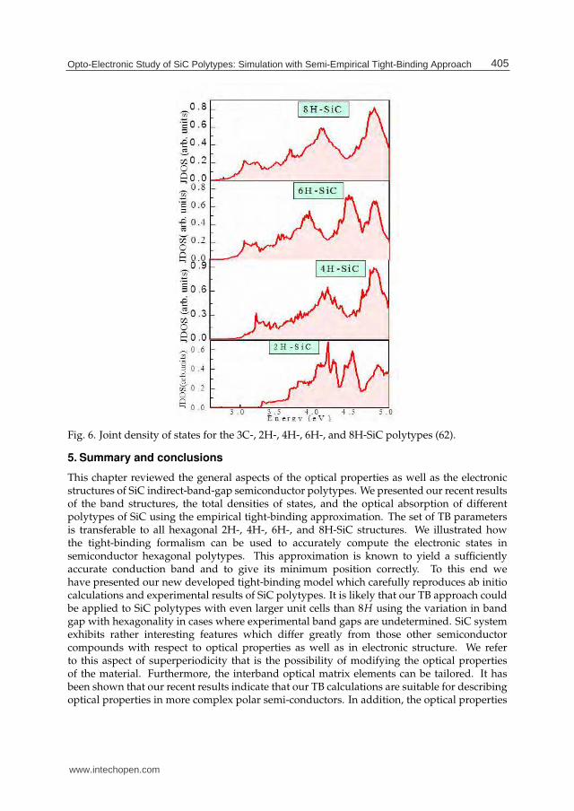
Before discussing the effect of the optical transition matrix elements, we consider the JDOS(see figure 6). In order to get more information on the interband transition, we presentour recent calculated joint density of states for SiC polytypes (62). We have determinedthe transition responsible for the major contributions to these structures. This was done byfinding the energy of the desired peak or shoulder on the joint density of states graph andthen examining the contribution to joint density of states at that energy from the constituentinterband transitions. The fundamental gap is well understood and is attributed to Γ15 →X1transition in 3C-SiC. We examine a large peak associated to Γ15 → L1 transition whichoccurs at 3.8 eV. The second major peak in JDOS, comes from the transition Γ15 → Γ1 whichoccurs at 5.2 eV. However, our band structure is satisfactory with respect to these transitions.The principal behavior of the joint density of states is very similar for the various 2H-, 4H-,6H-, 8H- polytypes considered. The two peaks below the ionic gap exhibit a different behaviorwith the number n of SiC bilayers in the unit cell. Whereas that at higher energy around 7 eV israther independent of the polytype, the low-energy peak around 8 eV is broadened with risingnumber n. We relate this fact to the folding effect parallel to the c axis. It causes an oppositevariation of the band curvature along the LM and HK lines in the hexagonal BZ (25), (73), (78).The intensity of the two most pronounced peaks at 3.5 and 2.1 eV in the region of the uppervalence bands monotonically follow the hexagonality of the structures (25), (75), (78),(79).Strong contributions to these peaks also arise from the LM line. The most drastic change inthe conduction band region occurs near the onset of the density of states. Its steepness overseveral eV again follows the hexagonality of the polytype. The particular shape of the onsethowever depends on the number of bilayers and therefore on the folding effect as already hasbeen pointed out by Lee et al. (84). The consequences can be clearly seen in the joint densityof states. Their low-energy tails increase with decreasing hexagonality.
404 Silicon Carbide – Materials, Processing and Applications in Electronic Devices
www.intechopen.com
Opto-Electronic Study of SiC Polytypes: Simulation with Semi-Empirical Tight-Binding Approach 17
Fig. 6. Joint density of states for the 3C-, 2H-, 4H-, 6H-, and 8H-SiC polytypes (62).
5. Summary and conclusions
This chapter reviewed the general aspects of the optical properties as well as the electronicstructures of SiC indirect-band-gap semiconductor polytypes. We presented our recent resultsof the band structures, the total densities of states, and the optical absorption of differentpolytypes of SiC using the empirical tight-binding approximation. The set of TB parametersis transferable to all hexagonal 2H-, 4H-, 6H-, and 8H-SiC structures. We illustrated howthe tight-binding formalism can be used to accurately compute the electronic states insemiconductor hexagonal polytypes. This approximation is known to yield a sufficientlyaccurate conduction band and to give its minimum position correctly. To this end wehave presented our new developed tight-binding model which carefully reproduces ab initiocalculations and experimental results of SiC polytypes. It is likely that our TB approach couldbe applied to SiC polytypes with even larger unit cells than 8H using the variation in bandgap with hexagonality in cases where experimental band gaps are undetermined. SiC systemexhibits rather interesting features which differ greatly from those other semiconductorcompounds with respect to optical properties as well as in electronic structure. We referto this aspect of superperiodicity that is the possibility of modifying the optical propertiesof the material. Furthermore, the interband optical matrix elements can be tailored. It hasbeen shown that our recent results indicate that our TB calculations are suitable for describingoptical properties in more complex polar semi-conductors. In addition, the optical properties
405Opto-Electronic Study of SiC Polytypes: Simulation with Semi-Empirical Tight-Binding Approach
www.intechopen.com

18 Silicon carbide
suggest that the hexagonal SiC polytypes composed of an indirect-band-gap semiconductorsoffer a great potential for application to optical devices.
6. References
[1] A. P Verma and P. Krishna, Polymorphism and Polytypism in Crystals, (Wiley, New York,1966).
[2] W. J. Choyke, in The Physics and Chemistry of Carbides, Nitrides and Borides, NATO ASI Ser.,Ser. E, Appl. Sci. Vol. 185, R Freer, Ed. (Kluver, Dordrecht, 1990), p. 563.
[3] K. Karch, G. Wellenhofer, P. Pavone, U. Röβler, and D. Strauch, Structural and ElectronicProperties of SiC polytypes, in Proceeding of 22nd International Conference On the Physicsof Semiconductors, Vancouver, 1994.
[4] R. F. Davis, Z. Sitar, B. E. Williams, H. S. Kong, H. J. Kim, J. W. Palmour, J. A. Edmond, J.Ryu, J. T. Glass, and C. H. Carter, Jr. Mater. Sci. Eng B 1, 77 (1988).
[5] N. W. Jepps and T. F. Page, Progr. Cryst. Growth Charact. 7, 259 (1983).[6] Diamond, SiC and Nitride Wide Bandgap Semiconductors, edited by C. H. Carter. Jr., et
al. (Materials Research Society, Pittsburgh, 1994).[7] P. Y. Yu, M. Cardona, Fundamentals of Semiconductors  Physics and Material
properties, Spinger (2005).[8] Silicon Carbide, III-Nitrides and Related Materials, edited by G. Pensl, H. Morko, B.
Monemar, and E. Janzn (Trans Tech publications, Switzerland, 1998).[9] D. B. Holt, B. G. Yacobi, Extended Defects in Semiconductors. Electronic Properties,
Device Effects and Structures, Cambridge University Press (2007).[10] V. I. Gavrilenko, A. V. Postnikov, N. I. Klyui, and V. G. Litovchenko, Phys. Stat. Sol. B 162,
447 (1990).[11] M. S. Miao, S. Limpijumnong, and W. R. L. Lambrecht, Appl. Phys. Lett. 79, 4360 (2001).[12] Walter R. L. Lambrecht and M. S. Miao, Phys. Rev. B 73, 155312 (2006).[13] C. Tivarus, J.P. Pelz, M.K. Hudait, S.A. Ringel, Appl. Phys. Lett. 87 182105 (2005).[14] K. J. Russell, Ian Appelbaum, and V. Narayanamurti, Phys. Rev. B 71, 121311(R) (2005).[15] W. R. L . Lambrecht, and B. Segall, Phys. Rev. B41, 2832 (1990).[16] K. Karch, G. Wellenhofer, P. Pavone, U. Röβler, and D. Strauch, Structural and Electronic
Properties of SiC polytypes, in Proceeding of 22nd International Conference On thePhysics of Semiconductors, Vancouver, 1994.
[17] J. Bernholc, A; Antonelli, C. Wang, and R. F. Davis, in Proceedings of the FifteenthInternational Conference on Defects in Semiconductors, Budapest, 1998.
[18] W. R. L. Lambrecht, B. Segall, M. Methfessel, and M. van Schilfgaarde, Phys. Rev. B 44,3685 (1991).
[19] W. R. L. Lambrecht, S. Limpijumnong, S. N. Rashkeev, and B. Segall, Phys. Stat. Sol. (b)202, 5 (1997).
[20] W. van Haeringen, P. A. Bobbert, and W. H. Backes, Phys. Stat. Sol. (b) 202, 63 (1997).[21] B. Adolph et al., Phys. Rev. B 55, 1422 (1997).[22] G. Pennington and N. Goldsman, Phys. Rev. B 64, 45104 (2001).[23] A. Bauer, Phys. Rev. B 57, 2647 (1998).[24] C. Person, and U. Lindefelt, J. Appl. Phys. 82, 5496 (1997).[25] P. Kckell, B. Wenzien, and F. Bechstedt, Phys. Rev. B 50, 10761 (1994).[26] C. Persson and U. Lindefelt, J. Appl. Phys. 82, 5496(1997).[27] W. J. Choyke, D. R. Hamilton, and Lyle Patrick, Phys. Rev. 133, 1163 (1964).[28] Lyle Patrick, D. R. Hamilton, and W. J. Choyke, Phys. Rev. 143, 526 (1994).
406 Silicon Carbide – Materials, Processing and Applications in Electronic Devices
www.intechopen.com
Opto-Electronic Study of SiC Polytypes: Simulation with Semi-Empirical Tight-Binding Approach 19
[29] A. O. Konstantinov and H. Bleichner, Appl. Phys. Lett. 71, 3700 (1997).[30] H. Lendenmann, F. Dahlquist, N. Johansson, R. Sonderholm, P. A. Nilsson, J. P. Bergman,
and P. Skytt, Mater. Sci. Forum 353-356, 727 (2001).[31] R. S. Okojie, M. Zhang, P. Pirouz, S. Tumakha, G. Jessen, and L. J. Brillson, Appl. Phys.
Lett. 79, 3056 (2001); Mater. Sci. Forum 389-393, 451 (2002).[32] L. J. Brillson, S. Tumakha, G. Jessen, R. S. Okojie, M. Zhang, and P. Pirouz, Appl. Phys.
Lett. 81, 2785 (2002).[33] H. Iwata, U. Lindefelt, S. berg, and P. R. Briddon, Mater. Sci. Forum 389-393, 439 (2002);
J. Appl. Phys. 93, 1577 (2003).[34] P. Pirouz, M. Zhang, J.-L. Demenet, and H. M. Hobgood, J. Appl. Phys. 93, 3279 (2003).[35] A. Galeckas, J. Linnros, and P. Pirouz, Appl. Phys. Lett. 81, 883 (2002).[36] A. T. Blumenau, C. J. Fall, R. Jones, S. berg, T. Frauenheim, and P. R. Briddon, Phys.
Rev. B 68, 174108 (2003).[37] A. T. Blumenau, R. Jones, S. berg, and T. Frauenheim, Mater. Sci. Forum 457- 460, 453
(2004).[38] P. O. A. Persson, L. Hultman, H. Jacobson, J. P. Bergman, E. Janzn, J. M.
Molina-Aldareguia, W. J. Clegg, and T. Tuomi, Appl. Phys. Lett. 80, 4852 (2002).[39] H.P. Iwata, U. Lindefelt, S. berg, P.R. Briddon, Phys. Rev. B, Vol. 65 (2001).[40] H.P. Iwata, U. Lindefelt, S. berg, P.R. Briddon, J. Phys. Condens. Matter Vol.14 p. 12733,
(2002).[41] H.P. Iwata, U. Lindefelt, S. berg, P.R. Briddon, Physica B, 340-342 p.165, (2003).[42] H.P. Iwata, U. Lindefelt, S. berg, P.R. Briddon, Microelectronics J. 34 371 (2003).[43] J. Camassel, S. Juillaguet, J. Phys. D: Appl.Phys. 40, 6264 (2007)[44] A. Chen, P. Srichaikul, Phys. Stat. Sol. B202, 81( 1997).[45] W.Y. Ching et al., Mater. Sci. And Eng. A 422, 147-156 (2006).[46] A. Galeckas, J. Linnros, B. Breitholtz, H. Bleichner, J. Appl. Phys. 90 (2) 980 (2001).[47] H. Iwata, U. Lindefelt, S. Oberg, and P. R. Briddon, Phys. Rev. B 65, 033203 (2001); Phys.
Rev. B 68, 245309 (2003).[48] T. G. Pedersen, K. Pedersen, and T. B. Kriestensen, Phys. Rev. B 63, 20110 (2001).[49] D. Vogel, P. Krüger, and J. Pollmann, Phys. Rev. B 52, R14316 (1995); B 54, 5495 (1996); B
55, 12836 (1997).[50] G. Litovchenko, Phys. Stat. Sol. B 162, 447 (1990).[51] G.L. Sun, I.G. Galben-Sandulache, T. Ouisse, J.M. Dedulle, M. Pons, R. Madar, D.
Chaussende, Mat. Sci. For. 645-648 (2010) pp 63-66.[52] Y. Ward, R. J. Young, R. A. Shatwell, J Mater Sci 42 (2007), p.5135-5141.[53] D. Chaussende, F. Baillet, L. Charpentier, E. Pernot, M. Pons, R. Madar, J. Electrochem.
Soc. Vol. 150, (2003), p. G653.[54] D. Chaussende, F. Mercier, A. Boulle, F. Conchon, M. Soueidan, G. Ferro, A. Mantzari, A.
Andreadou, E.K. Polychroniadis, C. Balloud, S. Juillaguet, J. Camassel, M. Pons, J. Cryst.Growth 310 (2008).
[55] S. Bai, R. P. Devaty, W. J. Choyke, U. Kaiser, G. Wagner, and M. F. MacMillan, Appl. Phys.Lett. 83, 3171 (2003).
[56] G. Zoulis, J. Sun, M. Beshkova, R. Vasiliauskas, S. Juillaguet, H. Peyre, M. Syvjrvi,R. Yakimova, J. Camassel, Mat. Sci. For. Vols. 645-648 (2010) pp 179-182.
[57] S. Ha, S. Skowronski, J.J. Sumakeris, M.J. Paisley, M.K. Kas Phys.Rev. Lett. Vol. 92, No.17, 175504 (2004).
407Opto-Electronic Study of SiC Polytypes: Simulation with Semi-Empirical Tight-Binding Approach
www.intechopen.com

20 Silicon carbide
[58] B. J. Skromme, K. Palle, C. D. Poweleit, L. R. Bryant, W. M. Vetter, M. Dudley, K. Moore,and T. Gehoski, Mater. Sci. Forum 389-393, 455 (2002); B. J. Skromme, K. C. Palle, M.K. Mikhov, H. Meidia, S. Mahajan, X. R. Huang, W. M. Vetter, M. Dudley, K. Moore, S.Smith, and T. Gehoski, Mater. Res. Soc. Symp. Proc. 742, 181 (2003).
[59] J. Q. Liu, H. J. Chung, T. Kuhr, Q. Li, and M. Skowronski, Appl. Phys. Lett. 80, 2111(2002).
[60] S. Izumi, H. Tsuchida, T. Tawara, I. Kamata, and K. Izumi, Mater. Sci. Forum 483-485,323 (2005); S. Izumi, H. Tsuchida, I. Kamata, and T. Tawara, Appl. Phys. Lett. 86, 202108(2005).
[61] H. Fujiwara, T. Kimoto, T. Tojo, and H. Matsunami, Appl. Phys. Lett. 87, 051912 (2005).[62] A. Laref, S. Laref, Phys. Stat. Sol. B 245, N1, 89-100 (2008).[63] I.G. Galben-Sandulache, G.L. Sun, J.M. Dedulle, T. Ouisse, R. Madar, M. Pons, D.
Chaussende, Mat. Sci. For. 645-648 (2010) pp 55-58.[64] L. Latu-Romain, D. Chaussende, C. Balloud, S. Juillaguet, L. Rapenne, E. Pernot, J.
Camassel, M. Pons, R. Madar, Mat. Sci. Forum, vols. 527-529 (2006), pp. 99-102.[65] A. A. Lebedev, P. L. Abramov, E. V. Bogdanova, S. P. Lebedev, D. K. Nelson, G. A.
Oganesyan, A. S. Tregubova, R Yakimova, Semicond. Sci. Technol. 23, 075004 (2008).[66] A. A. Lebedev, P. L. Abramov, N. V. Agrinskaya, V. I. Kozub, S. P. Lebedev, G. A.
Oganesyan, A. S. Tregubova, D. V. Shamshur, and M. O. Skvortsova, J. Appl. Phys. 105,023706 (2009).
[67] M. Skowronski and S. Ha, J. Appl. Phys. 99, 011101 (2006).[68] Y. Ward, R. J. Young, R. A. Shatwell, J Mater Sci 42 (2007), p.5135-5141.[69] T. Quisse, J. App. Phys. 75, 2092 (1994).[70] J. C. Slater and G.F. Koster, Phys. Rev 94, 1498 (1954).[71] P. Vogl and H. P. Hjalmarson, and J. D. Dow, J. Phys. Chem Solids 44, 365 (1983).[72] Y. C. Chang and D. E. Aspnes, Phys. Rev. B 41, 12002 (1990).[73] B. Wenzien, P. Käckell, F. Bechstedt, and G. Cappellini, Phys. Rev. B 52, 10897 (1995).[74] R. G. Humphreys, D. Bimberg, W. J. Choyke, Solid. State. Com . 39, 163 (1981).[75] Landolt-Börnstein, Numerical and Functional Relationships in Science and Technology, edited
by K. H. Hellwege (Spring-Verlag, Berlin, 1982).[76] G.Theodorou, G. Tsegas, and E. Kaxiras, J. Appl. Phys 85, 2179 (1999).[77] N. Bernstein, H. J. Gotsis, D. A. Papaconstantopoulos, and M. J. Mehl, Phys. Rev. B71,
075203 (2005).[78] G. Cubiotti, Yu. N. Kucherenko, and V. N. Antonov, J. Phys. Cond. Mat 9, 165 (1997).[79] J. Kuriplach, M. Sob, G. Brauer, W. Anwand, E.-M. Nicht, P. G. Coleman, and , N. Wagner,
Phys. Rev. B 59, 1948 (1999).[80] P.J. Colwell and M.V. Klein, Phys. Rev. B 6, 498 (1972).[81] N. T. Son et al., Appl. Phys. Lett 66, 107 (1995).[82] R. Kaplan, and R. J. Wagner, Solid State Com. 55, 67 (1985).[83] M. Willatzen, M. Cardona, and N. E. Christensen, Phys. Rev. B 51, 13150 (1995).[84] K, -H. Lee, C. H. Park, B. -H. Cheong, K. J. Chang, Solid State Commun. 92, 869 (1994).
408 Silicon Carbide – Materials, Processing and Applications in Electronic Devices
www.intechopen.com
Silicon Carbide - Materials, Processing and Applications inElectronic DevicesEdited by Dr. Moumita Mukherjee
ISBN 978-953-307-968-4Hard cover, 546 pagesPublisher InTechPublished online 10, October, 2011Published in print edition October, 2011
InTech EuropeUniversity Campus STeP Ri Slavka Krautzeka 83/A 51000 Rijeka, Croatia Phone: +385 (51) 770 447
InTech ChinaUnit 405, Office Block, Hotel Equatorial Shanghai No.65, Yan An Road (West), Shanghai, 200040, China
Phone: +86-21-62489820 Fax: +86-21-62489821
Silicon Carbide (SiC) and its polytypes, used primarily for grinding and high temperature ceramics, have beena part of human civilization for a long time. The inherent ability of SiC devices to operate with higher efficiencyand lower environmental footprint than silicon-based devices at high temperatures and under high voltagespushes SiC on the verge of becoming the material of choice for high power electronics and optoelectronics.What is more important, SiC is emerging to become a template for graphene fabrication, and a material for thenext generation of sub-32nm semiconductor devices. It is thus increasingly clear that SiC electronic systemswill dominate the new energy and transport technologies of the 21st century. In 21 chapters of the book,special emphasis has been placed on the “materials†aspects and developments thereof. To that end,about 70% of the book addresses the theory, crystal growth, defects, surface and interface properties,characterization, and processing issues pertaining to SiC. The remaining 30% of the book covers theelectronic device aspects of this material. Overall, this book will be valuable as a reference for SiC researchersfor a few years to come. This book prestigiously covers our current understanding of SiC as a semiconductormaterial in electronics. The primary target for the book includes students, researchers, material and chemicalengineers, semiconductor manufacturers and professionals who are interested in silicon carbide and itscontinuing progression.
How to referenceIn order to correctly reference this scholarly work, feel free to copy and paste the following:
Amel Laref and Slimane Laref (2011). Opto-Electronic Study of SiC Polytypes: Simulation with Semi-EmpiricalTight-Binding Approach, Silicon Carbide - Materials, Processing and Applications in Electronic Devices, Dr.Moumita Mukherjee (Ed.), ISBN: 978-953-307-968-4, InTech, Available from:http://www.intechopen.com/books/silicon-carbide-materials-processing-and-applications-in-electronic-devices/opto-electronic-study-of-sic-polytypes-simulation-with-semi-empirical-tight-binding-approach
www.intechopen.com

Fax: +385 (51) 686 166www.intechopen.com
Fax: +86-21-62489821

© 2011 The Author(s). Licensee IntechOpen. This is an open access articledistributed under the terms of the Creative Commons Attribution 3.0License, which permits unrestricted use, distribution, and reproduction inany medium, provided the original work is properly cited.