Embed Size (px)
Citation preview

SANDIA REPORT SAND2009-5965Unlimited Release
Printed September 2009
Optimized Nanoporous Materials David B. Robinson, Chung-An Max Wu, Benjamin W. Jacobs, Markus D. Ong, Kim L. Tran, Mary E. Langham, Cindy M. Ha, Dara V. Gough, Paul V. Braun, Weon-Sik Chae, Sung-Kyoung Ham, Shaun D. Gittard, Bonnie E. Pierson, and Roger J. Narayan Prepared by Sandia National Laboratories Albuquerque, New Mexico 87185 and Livermore, California 94550
Sandia is a multiprogram laboratory operated by Sandia Corporation, a Lockheed Martin Company, for the United States Department of Energy’s National Nuclear Security Administration under Contract DE-AC04-94AL85000.
Approved for public release; further dissemination unlimited.
2
Issued by Sandia National Laboratories, operated for the United States Department of Energy by Sandia Corporation. NOTICE: This report was prepared as an account of work sponsored by an agency of the United States Government. Neither the United States Government, nor any agency thereof, nor any of their employees, nor any of their contractors, subcontractors, or their employees, make any warranty, express or implied, or assume any legal liability or responsibility for the accuracy, completeness, or usefulness of any information, apparatus, product, or process disclosed, or represent that its use would not infringe privately owned rights. Reference herein to any specific commercial product, process, or service by trade name, trademark, manufacturer, or otherwise, does not necessarily constitute or imply its endorsement, recommendation, or favoring by the United States Government, any agency thereof, or any of their contractors or subcontractors. The views and opinions expressed herein do not necessarily state or reflect those of the United States Government, any agency thereof, or any of their contractors. Printed in the United States of America. This report has been reproduced directly from the best available copy. Available to DOE and DOE contractors from U.S. Department of Energy Office of Scientific and Technical Information P.O. Box 62 Oak Ridge, TN 37831 Telephone: (865) 576-8401 Facsimile: (865) 576-5728 E-Mail: [email protected] Online ordering: http://www.osti.gov/bridge Available to the public from U.S. Department of Commerce National Technical Information Service 5285 Port Royal Rd. Springfield, VA 22161 Telephone: (800) 553-6847 Facsimile: (703) 605-6900 E-Mail: [email protected] Online order: http://www.ntis.gov/help/ordermethods.asp?loc=7-4-0#online
3
SAND2009-5965Unlimited Release
Printed September 2009
Optimized Nanoporous Materials
David B. Robinson, Chung-An Max Wu, Benjamin W. Jacobs, Markus D. Ong, Kim L. Tran, Mary E. Langham, and Cindy M. Ha Energy Nanomaterials Dept. (8651)
Sandia National Laboratories P.O. Box 969
Livermore, CA 94551
Dara V. Gough and Paul V. Braun Department of Materials Science and Engineering
University of Illinois at Urbana-Champaign Urbana, IL 61801
Weon-Sik Chae and Sung-Kyoung Ham
Gangneung Center, Korea Basic Science Institute, Gangneung, South Korea 210-702
Shaun D. Gittard, Bonnie E. Pierson, and Roger J. Narayan UNC/NCSU Joint Department of Biomedical Engineering
North Carolina State University Raleigh, NC 27695-7115
Abstract
Nanoporous materials have maximum practical surface areas for electrical charge storage; every point in an electrode is within a few atoms of an interface at which charge can be stored. Metal-electrolyte interfaces make best use of surface area in porous materials. However, ion transport through long, narrow pores is slow. We seek to understand and optimize the tradeoff between capacity and transport. Modeling and measurements of nanoporous gold electrodes has allowed us to determine design principles, including the fact that these materials can deplete salt from the electrolyte, increasing resistance. We have developed fabrication techniques to demonstrate architectures inspired by these principles that may overcome identified obstacles. A key concept is that electrodes should be as close together as possible; this is likely to involve an interpenetrating pore structure. However, this may prove extremely challenging to fabricate at the finest scales; a hierarchically porous structure can be a worthy compromise.

4

5
ACKNOWLEDGMENTS This project was supported by the National Institute for Nano Engineering, part of the Laboratory-Directed Research and Development program at Sandia National Laboratories. Funds for the North Carolina authors were provided by the National Science Foundation. Max Wu and Cindy Ha were funded in part by National Nuclear Security Administration High School Science Bowl internships. Stewart Griffiths and Eric Majzoub initially helped define the project concept.
6
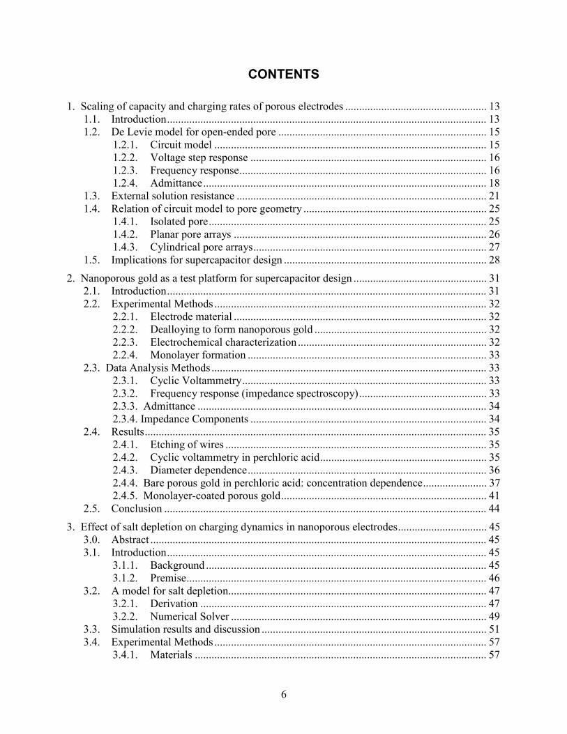
CONTENTS
1. Scaling of capacity and charging rates of porous electrodes ................................................... 13 1.1. Introduction................................................................................................................... 13 1.2. De Levie model for open-ended pore ........................................................................... 15
1.2.1. Circuit model .................................................................................................. 15 1.2.2. Voltage step response ..................................................................................... 16 1.2.3. Frequency response......................................................................................... 16 1.2.4. Admittance...................................................................................................... 18
1.3. External solution resistance .......................................................................................... 21 1.4. Relation of circuit model to pore geometry .................................................................. 25
1.4.1. Isolated pore.................................................................................................... 25 1.4.2. Planar pore arrays ........................................................................................... 26 1.4.3. Cylindrical pore arrays.................................................................................... 27
1.5. Implications for supercapacitor design ......................................................................... 28
2. Nanoporous gold as a test platform for supercapacitor design ................................................ 31 2.1. Introduction................................................................................................................... 31 2.2. Experimental Methods .................................................................................................. 32
2.2.1. Electrode material ........................................................................................... 32 2.2.2. Dealloying to form nanoporous gold .............................................................. 32 2.2.3. Electrochemical characterization .................................................................... 32 2.2.4. Monolayer formation ...................................................................................... 33
2.3. Data Analysis Methods ................................................................................................... 33 2.3.1. Cyclic Voltammetry........................................................................................ 33 2.3.2. Frequency response (impedance spectroscopy).............................................. 33 2.3.3. Admittance ........................................................................................................ 34 2.3.4. Impedance Components ..................................................................................... 34
2.4. Results........................................................................................................................... 35 2.4.1. Etching of wires .............................................................................................. 35 2.4.2. Cyclic voltammetry in perchloric acid............................................................ 35 2.4.3. Diameter dependence...................................................................................... 36 2.4.4. Bare porous gold in perchloric acid: concentration dependence....................... 37 2.4.5. Monolayer-coated porous gold.......................................................................... 41
2.5. Conclusion .................................................................................................................... 44
3. Effect of salt depletion on charging dynamics in nanoporous electrodes................................ 45 3.0. Abstract ......................................................................................................................... 45 3.1. Introduction................................................................................................................... 45
3.1.1. Background ..................................................................................................... 45 3.1.2. Premise............................................................................................................ 46
3.2. A model for salt depletion............................................................................................. 47 3.2.1. Derivation ....................................................................................................... 47 3.2.2. Numerical Solver ............................................................................................ 49
3.3. Simulation results and discussion ................................................................................. 51 3.4. Experimental Methods .................................................................................................. 57
3.4.1. Materials ......................................................................................................... 57
7
3.4.2. Dealloying to form nanoporous gold .............................................................. 57 3.4.3. Two-electrode cell .......................................................................................... 58 3.4.4. Three-electrode cell ........................................................................................ 58 3.4.5. Characterization .............................................................................................. 58
3.5. Experimental results and discussion ............................................................................. 58 3.5.1. Two-electrode cell with sodium trifluoroacetate ............................................ 58 3.5.2. Two-electrode cell with trifluoroacetic acid ................................................... 62 3.5.3. Three-electrode cell with sodium trifluoroacetate .......................................... 62 3.5.4. Frequency response......................................................................................... 64
3.6. Conclusion .................................................................................................................... 65
4. Electrically triggered drug delivery using nanoporous electrodes........................................... 67 4.0. Abstract ......................................................................................................................... 67 4.1. Introduction................................................................................................................... 67
4.1.1. Background ..................................................................................................... 67 4.1.2. Capacitive delivery ......................................................................................... 69
4.2. Experimental Methods .................................................................................................. 71 4.2.1. Dealloying to form nanoporous gold .............................................................. 71 4.2.2. Analysis of gold wire ...................................................................................... 71 4.2.3. Cell setup ........................................................................................................ 71 4.2.4. Electrochemical characterization .................................................................... 72 4.2.5. UV spectroscopy............................................................................................. 72
4.3. Results and Discussion ................................................................................................. 73 4.3.1. Electrode fabrication....................................................................................... 73 4.3.2. Cyclic voltammetry......................................................................................... 74 4.3.3. Step height dependence................................................................................... 75 4.3.4. Reversibility of charging: sodium trifluoroacetate ......................................... 76 4.3.5. Reversibility of charging: Magnesium sulfate................................................ 77 4.3.6. Discharge of benzylammonium salicylate into sodium trifluoroacetate......... 78 4.3.7. Discharge of benzylammonium salicylate into magnesium sulfate................ 80
4.4. Conclusion .................................................................................................................... 81
5. Bimodally porous electrode materials ..................................................................................... 83 5.0. Abstract ......................................................................................................................... 83 5.1. Introduction................................................................................................................... 83 5.2. Experimental Details..................................................................................................... 84
5.2.1. Preparation of polystyrene colloidal assemblies............................................. 84 5.2.2. Preparation of silica inverse opal using the polystyrene opal templates ........ 84 5.2.3. Electrochemical deposition of bimodal porous gold materials....................... 85 5.2.4. Preparation of mesoporous carbon ball assembly........................................... 85 5.2.5. Characterization .............................................................................................. 86
5.3. Results and Discussion ................................................................................................. 86 5.3.1. Bimodal nanoporous gold electrodes.............................................................. 86 5.3.2. Bimodal nanoporous carbon materials............................................................ 91
5.4. Other approaches .......................................................................................................... 92 5.5. Conclusion .................................................................................................................... 93
6. Fabrication of interpenetrating dielectric capacitors................................................................ 95
8
6.0. Abstract ......................................................................................................................... 95 6.1. Introduction................................................................................................................... 95
6.1.1. Background ..................................................................................................... 95 6.1.2. Related work. .................................................................................................. 96 6.1.3. Essence of concept.......................................................................................... 96 6.1.4. Substrate conductor......................................................................................... 97 6.1.5. Conformal dielectric layer .............................................................................. 97 6.1.6. Matching conductor deposition....................................................................... 98 6.1.7. Experimental scope......................................................................................... 98
6.2. Device fabrication......................................................................................................... 98 6.3. Results......................................................................................................................... 100 6.4. Conclusions and future work ...................................................................................... 103
7. Future opportunities for supercapacitors ............................................................................... 105 7.1. Background ................................................................................................................. 105 7.2. Ion behavior in nanoporous supercapacitor electrodes............................................... 105 7.3. Achieving physical limits of supercapacitor performance.......................................... 106 7.4. Impact on DOE mission.............................................................................................. 107
7.4.1. Transportation applications........................................................................... 107 7.4.2. Renewable electricity applications ............................................................... 108 7.4.3. Impact on energy-related fields .................................................................... 108 7.4.4. DOE mission areas........................................................................................ 110
8. References.............................................................................................................................. 111
Appendix: salt depletion simulation code.................................................................................. 117
9
FIGURES Figure 1-1. Dielectric capacitor. .................................................................................................. 13 Figure 1-2. Double-layer capacitor, with ion-conducting medium between electrodes. ............. 14 Figure 1-3. Geometry of pore model, and circuit model for half of open-ended pore. ............... 15 R represents resistance per unit length, while C represents capacitance per unit length. ............. 15 Figure 1-4. Admittance magnitude for unit pore open at both ends (RL/2, CL = 1).................... 19 Figure 1-5. Admittance phase for unit pore open at both ends (RL/2, CL = 1). .......................... 20 Figure 1-6. Nyquist plot for unit pore open at both ends (RL/2, CL = 1). ................................... 20 Figure 1-7. Admittance magnitude for unit pore open at both ends (RL/2, CL = 1) and external
solution resistance Rx of 0, 1/6, or 1 ohm (top to bottom). ........................................................ 22 Figure 1-8. Admittance phase for unit pore open at both ends (RL/2, CL = 1) and external
solution resistance Rx of 0, 1/6, or 1 ohm (top to bottom). ........................................................ 23 Figure 1-9. Nyquist plot for unit pore open at both ends (RL/2, CL = 1) and external solution
resistance Rx of 0, 1/6, or 1 ohm (left to right)........................................................................... 23 Figure 1-10. Effective capacitance (charge divided by voltage magnitude) for unit pore open at
both ends (RL/2, CL = 1) and external solution resistance Rx of 0, 1/6, or 1 ohm (right to left)..................................................................................................................................................... 24
Figure 1-11. External resistance at end of a pore involves hemispherical conduction paths. ..... 25 Figure 1-12. External resistance at end of close-packed pores involves confined conduction
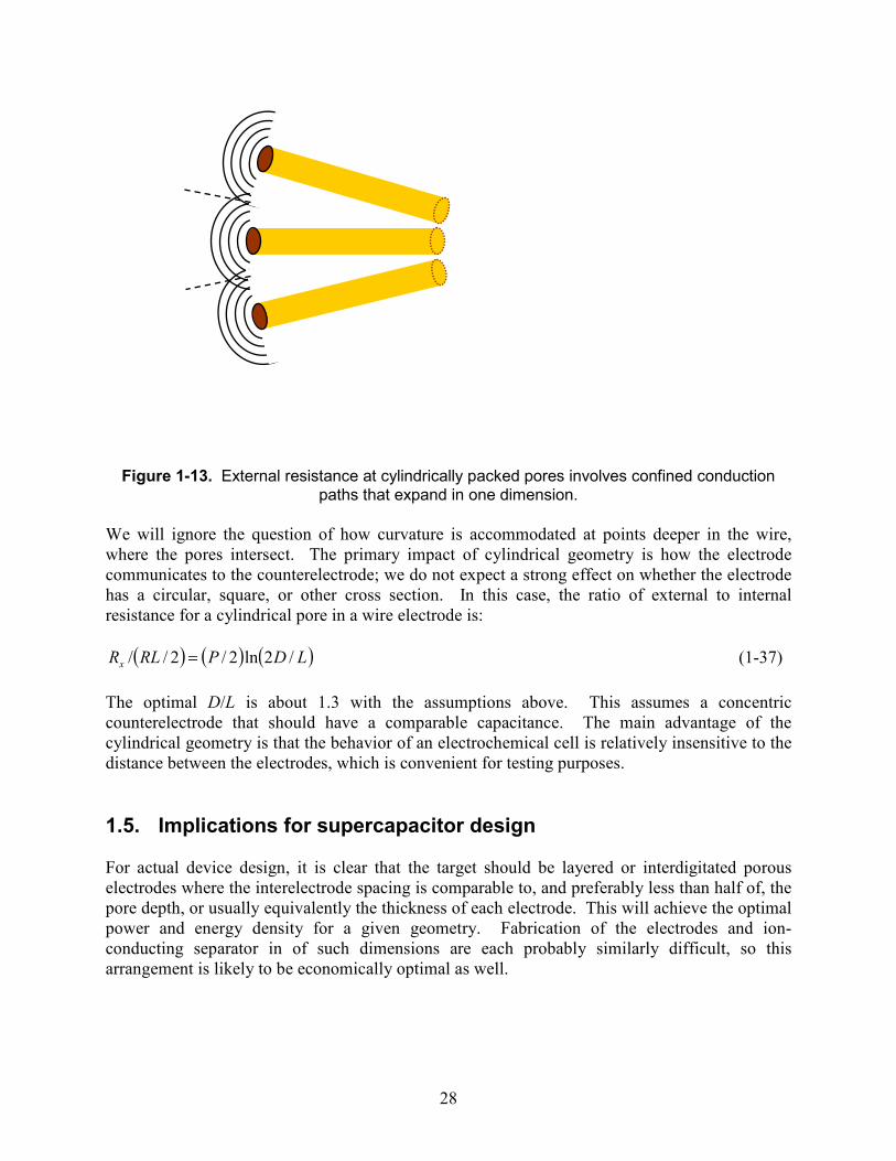
paths. .......................................................................................................................................... 27 Figure 1-13. External resistance at cylindrically packed pores involves confined conduction
paths that expand in one dimension. .......................................................................................... 28 Figure 2-1. Etched porous gold wire............................................................................................ 35 Figure 2-2. Bode plot of log admittance versus log frequency with a bare gold electrode in
HClO4 electrolyte....................................................................................................................... 36 Figure 2-3. Frequency response (left) and capacitance (right) of etched porous gold wire as a
function of wire diameter........................................................................................................... 37 Figure 2-4. Bode plot of log admittance versus log frequency with a bare gold electrode in
HClO4 electrolyte. Blue lines are fits to the model................................................................... 38 Figure 2-5. Real component of impedance plotted vs imaginary component of impedance....... 39 0.2mm diameter, 2 cm gold wire electrode in HClO4 electrolyte. Input frequency increases from
top to bottom of each curve. ...................................................................................................... 39 Figure 2-6. Bode plot of log admittance versus log frequency with a bare gold electrode in
HClO4 electrolyte....................................................................................................................... 40 Figure 2-7. Bode plot of log admittance versus log frequency with a bare gold electrode in
HClO4 electrolyte....................................................................................................................... 41 Figure 2-8. Admittance magnitudes of bare and hydroxy-C6-thiolated porous gold electrodes in
1M aqueous HClO4 or tetramethylammonium lactate............................................................... 42 Figure 2-9. Nyquist plot of bare and hydroxy-C6-thiolated gold electrodes in 1M aqueous
HClO4 or tetramethylammonium lactate. .................................................................................. 43 Figure 3-1. De Levie’s transmission line equivalent circuit for an electrolyte-filled conducting
pore. ........................................................................................................................................... 47 Figure 3-2. Extension of circuit model outside pore.................................................................... 50
10
Figure 3-3. Box-shaped simulated cyclic voltammogram for 30 mM electrolyte, 10 nm x 100 µm pore, 20 µm external region, 7.5 mV/s (periodic boundary conditions). ............................ 52
Figure 3-4. Leaf-shaped simulated cyclic voltammogram for 30 mM electrolyte, 10 nm x 100 µm pore, 20 µm external region, 2.4 V/s (periodic boundary conditions). ............................... 53
Figure 3-5. Liver-shaped simulated cyclic voltammogram for 30 mM electrolyte, 10 nm x 100 µm pore, 20 µm external region, 300 mV/s (periodic boundary conditions). ........................... 54
Figure 3-6. Lobed-liver simulated cyclic voltammogram for 15 mM electrolyte, 10 nm x 100 µm pore, 20 µm external region, 37.5 mV/s (periodic boundary conditions).................................. 55
Figure 3-7. simulated cyclic voltammogram for 300 mM electrolyte, 10 nm x 100 µm pore, 20 µm external region (periodic boundary conditions), normalized by scan rates, which differ by factors of 2 except for 7.5 mV/s................................................................................................. 56
Figure 3-8. simulated cyclic voltammogram for 30 mM electrolyte, 10 nm x 100 µm pore, 20 µm (black) or 80 µm (red) external region (periodic boundary conditions).............................. 57
Figure 3-9. Experimental voltammograms for two-electrode porous gold wire cells in 30 mM sodium trifluoroacetate at varying scan rates. The left and right plots show the same 10 and 60 mV/s scans on different scales. .................................................................................................. 59
Figure 3-10. Experimental voltammograms for two-electrode porous gold wire cells in 10 mM sodium trifluoroacetate at varying scan rates............................................................................. 60
Figure 3-11. Experimental voltammograms for two-electrode porous gold wire cells in 10 mM sodium trifluoroacetate with varying scan directions. ............................................................... 60
Figure 3-12. Sequential experimental voltammograms for two porous gold wires in sodium trifluoroacetate. .......................................................................................................................... 61
Figure 3-13. Experimental voltammograms for two-electrode porous gold wire cells in 10 mM or 30 mM trifluoroacetic acid at varying scan rates. ................................................................. 62
Figure 3-14. Three-electrode voltammograms vs. Ag/AgCl for porous gold wire at 10 mV/s and 10 mM sodium trifluoroacetate.................................................................................................. 63
Figure 3-15. Nyquist plots for two-electrode cells in 30 mM or 100 mM sodium trifluoroacetate (along with a simulation result for the latter), and 30 mM trifluoroacetic acid......................... 64
Figure 4-1. (a) Diagram of electrochemical dealloying of Au-Ag alloy to produce nanoporous gold electrodes. (b) Chemical structure of sodium trifluoroacetate (NaTFA) and benzylammonium salicylate, the two analytes examined in this study. (c) Diagram of experiment testing capacitive storage and delivery of benzylammonium salicylate. ................ 73
Figure 4-2. Characterization of etching process. (a) Scanning electron micrograph of nano-porous gold electrode produced by electrochemical etching. The average pore diameter is 10 ± 5 nm. (b) Energy dispersive X-ray spectra of etched nano-porous wire with background subtracted. The wires are 94.86% weight gold and 5.14% weight silver. ................................ 74
Figure 4-3. Electrochemical characterization of nanoporous electrodes. (a) CV of 100 mM NaTFA, (c) CV of 50 mM Benzylammonium salicylate at a 5 mV/s scan rate, (c) CA of 100 mM NaTFA with 100 mV and 200 mV applied, (d) CA of 50 mM benzylammonium salicylate with 100 mV and 200 mV applied. ............................................................................................ 75
Figure 4-4. Charge, transfer, and discharge of wire with sodium trifluoroacetate at indicated concentrations. Discharge curves are inverted and superimposed on charge curves. More points were collected than are indicated by the symbols........................................................... 76
Figure 4-5. Charge, transfer, and discharge of wire with magneium sulfate at indicated concentrations. Discharge curves are inverted and superimposed on charge curves. More points were collected than are indicated by the symbols........................................................... 77
11
Figure 4-6. Absorbance of varying concentrations of benzylammonium salicylate in a 4 mL PMMA cuvette after background subtraction............................................................................ 78
Figure 4-7. UV-Vis absorption of benzylammonium salicylate (BzAmSal) electrostatically stored in electrodes and delivered into 4 ml of 10 mM NaTFA. ............................................... 79
Figure 5-1. Experimental setup for the preparation of polystyrene colloidal opals...................... 84 Figure 5-2. Scheme of preparation of bimodal porous gold materials via a double templating
route. .......................................................................................................................................... 85 Figure 5-3. Scheme of preparation of bimodal porous carbon material via a triple templating
route. .......................................................................................................................................... 85 Figure 5-4. (A) A polystyrene colloidal assembly grown on an evaporated gold substrate and (B)
silica inverse opal prepared from the ordered polystyrene colloidal assembly. Insets are a representative picture (upper) and a cross-sectional view (lower) for the polystyrene opal. .... 86
Figure 5-5. (A) A polystyrene colloidal assembly grown on an electrochemically deposited gold film on an evaporated gold substrate and (B) silica inverse opal prepared from the disordered polystyrene colloidal assembly. Inset is a cross-sectional view. ............................................... 87
Figure 5-6. Electrochemically grown p-Au bulk film. Inset is a cross-sectional view with an average thickness of ~1.43 µm and a pore size of ~10 nm........................................................ 88
Figure 5-7. (A) Electrochemically grown p-Au opal using the ordered silica inverse opal template. Inset is a cross-sectional view with an average thickness of ~1.43 µm. (B) The magnified image clearly presents unique bimodal porosity. ..................................................... 88
Figure 5-8. (A) Electrochemically grown p-Au opal using the disordered silica inverse opal template. (B) The magnified image clearly presents unique bimodal porosity. ........................ 89
Figure 5-9. CV for the gold electrodes of different micro- and nanoarchitectures in 1 M H2SO4 aqueous solution at a scan rate of 50mV/s................................................................................. 89
Figure 5-10. CV for the porous Au bulk film in 1 M H2SO4 aqueous solution at different scan rates. ........................................................................................................................................... 90
Figure 5-11. Peak shift due to varying scan rates for the porous gold film electrode compared with peak shifts at 50 mV/s for opal electrodes. ........................................................................ 91
Figure 5-12. Electron microscope images of (A) the silica inverse opal, (B) the mesoporous silica balls within the silica inverse opal, (c) the carbon ball assembly, and (d) the component mesoporous carbon balls............................................................................................................ 92
Figure 5-13. SEM images of the porous alumina template (left) and the replicated p-Au nanofiber assembly (right). ........................................................................................................ 92
Figure 5-14. SEM image of the polystyrene colloidal particles (left) and its snapshot image (right). ........................................................................................................................................ 93
Figure 6-1. Dielectric capacitor. .................................................................................................. 95 Figure 6-2: Hierarchically porous carbon and gold, as described in the previous chapter, and
porous platinum powders.Robinson, 2009............................................................................. 97 Figure 6-3. Preparation procedure for inverse opal metal-insulator-metal structures. (a) Opal
template is formed by vertical deposition of colloidal polystyrene at the drying front of the liquid on the Au substrate. (b) Ni is electrodeposited into the opal template. (c) Polystyrene colloids are dissolved in THF, resulting in Ni inverse opal. (d) Dielectric material is conformally deposited within the Ni inverse opal by atomic layer deposition. (e) Counterelectrode is conformally deposited using electroless plating or atomic layer deposition..................................................................................................................................................... 99
12
Figure 6-4. Representation of PMMA masking the bottom electrode to prevent a short circuit prior to deposition of the top electrode. ................................................................................... 100
Figure 6-5: (left) SEM image of a Ni inverse opal formed by vertical deposition of 466 nm polystyrene colloids. (right) Cyclic voltammogram of Ni coated with ca. 10 nm Al2O3 by atomic layer deposition. 100 mV/s in 1 mg/mL each of potassium ferri- and ferrocyanide. . 101
Figure 6-6. Top: SEM images showing both top (left) and cross section (right) views of a metal-insulator-metal structure formed by Ni electrodeposition into a 3-D template, removal of the template, atomic layer deposition of the dielectric, and atomic layer deposition of a Pt top electrode. For cross sections, samples tend to cleave at the necks between spheres. Bottom: Energy dispersive spectroscopy (EDS) data collected showing successful deposition of platinum into a 3-D structure collected from the sample shown above................................... 102
Figure 6-7. SEM images showing top (left) and cross section (right) views of a metal-insulator-metal structure formed by Ni electrodeposition into a 3-D template, removal of the template, atomic layer deposition of the dielectric, and electroless plating of a Au top electrode. ........ 102
Figure 7-1. Power density versus energy density for various electrical energy storage devices, as reported in the DOE’s Basic Research Needs for Electrical Energy Storage Workshop Report. Points added to the plot are mentioned in the text, some of which exceed the scale (teal = electrostatic, blue = electrochemical). ..................................................................................... 109
TABLES Table 1-1. Porosity parameter P for various arrangements of cylindrical pores. The spacing is in
units of pore radius..................................................................................................................... 26 Table 2-1. A sample data array for one of the characterized wires. ............................................ 34 Table 2-2. Parameters used to fit HClO4 concentration dependence data to the model. ............. 39 Table 2-3. Parameters used to fit monolayer data to the model................................................... 44 Table 3-1. Salt concentration needed to charge nanoporous metal electrode vs. pore diameter. 46 Table 4-1. Theoretical storage capacity versus pore diameter for porous capacitors. .................. 70 Table 4-2. Charge stored by wires as calculated from Figure 4-3c,d. .......................................... 76 Table 4-3. Release of benzylammonium salicylate into 10 mM NaTFA measured via UV
spectroscopy and by chronoamperometry. ................................................................................ 79 Table 4-4. Release of benzylammonium salicylate into 30 mM MgSO4 measured via UV
spectroscopy and by chronoamperometry. ................................................................................ 80
13
1. SCALING OF CAPACITY AND CHARGING RATES OF POROUS ELECTRODES
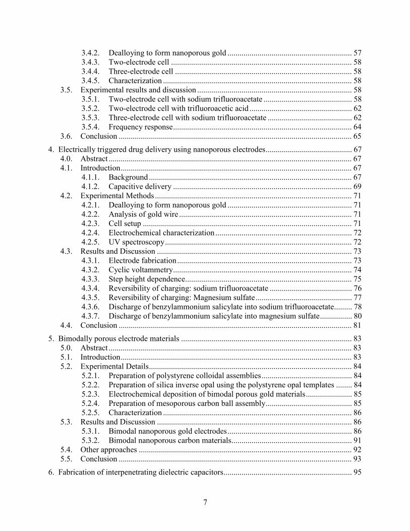
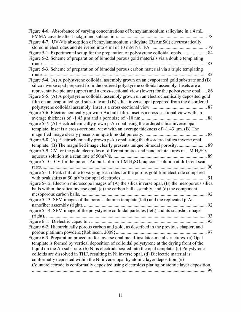
1.1. Introduction Capacitors are devices that store energy in an electric field between a pair of conducting materials. They can deliver this energy rapidly, often limited by the resistance of the electrical contacts to the device or other external parameters. The energy stored per unit volume or mass is lower than devices that employ chemical change, such as batteries and fuel cells, but their high power makes them complementary to these devices, increasing peak power input and output. They are also important as circuit elements in signal processing and general electronics applications.[1] One of the most important factors to consider in the construction of a capacitor is the amount of interfacial surface between the conductors. Because capacitance scales proportionally to each conducting plate’s area, a conceptually easy and experimentally controllable method to increase the energy capacity of the device is to increase its surface area. An electrostatic capacitor stores energy E according to:
Q = charge C = capacitance ε = dielectric constant A = electrode area V = voltage d = dielectric thickness δ = conductor thickness
Figure 1-1. Dielectric capacitor.
Adjusting these parameters can maximize the stored energy. d is limited by complicated dielectric breakdown mechanisms, but can be maintained in the nanometer range at low voltages. The dielectric constant can be made large, but cannot make the effective d less than an atomic separation. For a given device volume and voltage, maximizing A is the best opportunity to maximize E. To achieve this, the conductor thickness δ should also be in the nanometer range: throughout the volume of the device, at any point in one conductor, the other conductor must be only a few nanometers away, separated by the insulating dielectric. Devices that approach this ideal are called supercapacitors. A second major consideration is the electrical resistance of the long, narrow conduction paths implied by this arrangement, which we will also address. To a first approximation, dielectric breakdown occurs at a specific electric field Emax.[2] If the conductor can be assumed to be thin compared to the dielectric layer, the device volume is Ad and the energy stored per unit volume is ½εEmax. This suggests that the maximum stored energy
22
21
21
21 V
d
ACVQVE ε===
L
+
+
+
+
+
+
+
+
+
A
+ +
+ +
+ +
+ +
+ +
V
δd
14
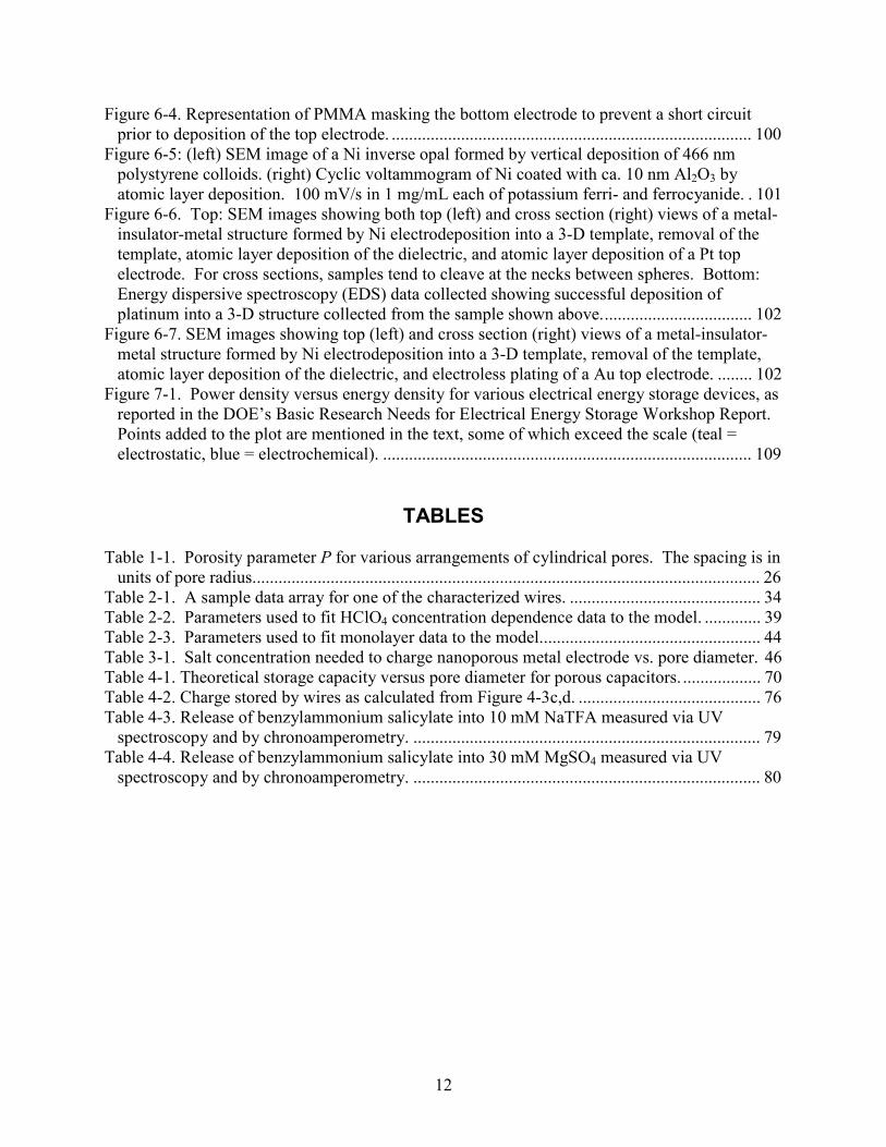
is independent of device geometry. In this case there is a tradeoff between dielectric thickness, which translates to pore size in a supercapacitor, and operating voltage. A nanoporous device can store the same amount of energy at lower voltage than a coarser device. This is safer, requires less external insulation, and reduces the need for circuitry that interconverts voltages. In an alternative architecture, shown in Figure 1-2, the dielectric layer is replaced by an ion conductor such as an aqueous salt solution. Normally, the ions do not penetrate into the electrode or change their charge state due to chemical reaction at the electrode, but instead approach the electrode with near-atomic spacing, causing the dielectric thickness d to approach the smallest conceivable value. The ion-electrode interface is known as the double layer. There are additional benefits: if the electrodes are porous materials, ions can penetrate into very small pores, comparable to their size. Pore diameter is not limited by the capabilities of fabrication methods for electrodes or dielectric layers, so higher areas can be achieved. Ion conductors are not subject to the same breakdown mechanisms as dielectrics, which are sensitive to geometry and atom-scale defects. Disadvantages are that breakdown can involve chemical changes induced at relatively low voltages; liquid electrolytes can present hazards upon leakage of the device; and ion conductivity is much slower than electrical conductivity or dielectric relaxation, resulting in slow charging times. Pores are long and narrow, and resistance increases with length and decreases with cross-sectional area, so this can be significant.
Figure 1-2. Double-layer capacitor, with ion-conducting medium between electrodes.
An optimal architecture for a supercapacitor, then, is likely to involve fabrication of electrodes that interpenetrate on a scale limited by capabilities of fabrication techniques, and perhaps by other engineering criteria including geometric, mechanical, and thermal constraints. The electrodes are separated by an ion conductor that can penetrate smaller-scale pores in each electrode.
+
+
+
+
+
+
+
+
+
A
V
+
+
+
+
+
+
+
+
D
d
15
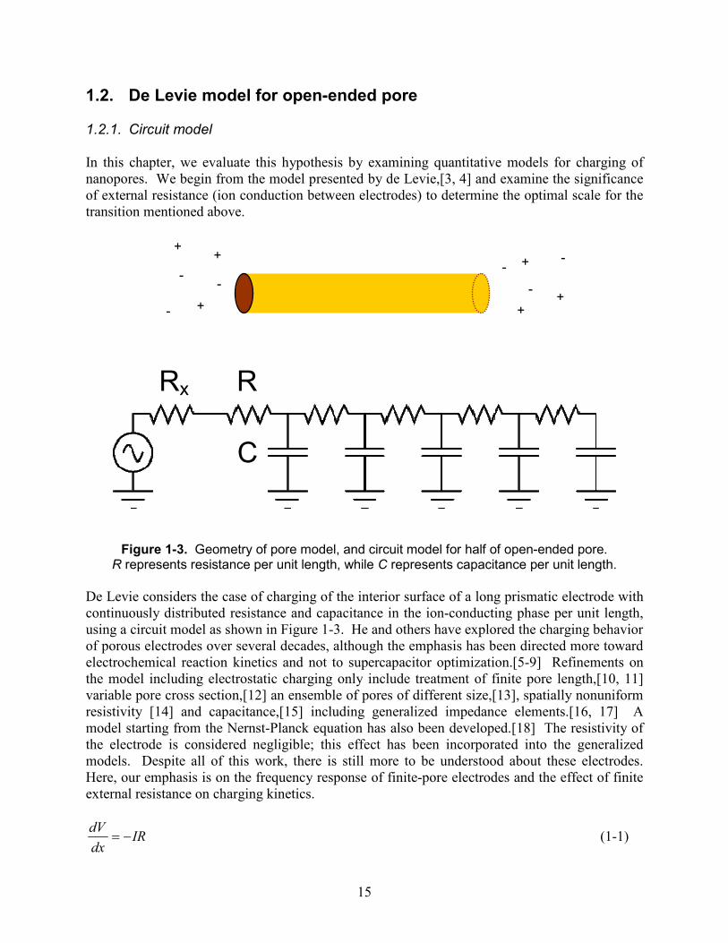
1.2. De Levie model for open-ended pore 1.2.1. Circuit model In this chapter, we evaluate this hypothesis by examining quantitative models for charging of nanopores. We begin from the model presented by de Levie,[3, 4] and examine the significance of external resistance (ion conduction between electrodes) to determine the optimal scale for the transition mentioned above.
Figure 1-3. Geometry of pore model, and circuit model for half of open-ended pore. R represents resistance per unit length, while C represents capacitance per unit length.
De Levie considers the case of charging of the interior surface of a long prismatic electrode with continuously distributed resistance and capacitance in the ion-conducting phase per unit length, using a circuit model as shown in Figure 1-3. He and others have explored the charging behavior of porous electrodes over several decades, although the emphasis has been directed more toward electrochemical reaction kinetics and not to supercapacitor optimization.[5-9] Refinements on the model including electrostatic charging only include treatment of finite pore length,[10, 11] variable pore cross section,[12] an ensemble of pores of different size,[13], spatially nonuniform resistivity [14] and capacitance,[15] including generalized impedance elements.[16, 17] A model starting from the Nernst-Planck equation has also been developed.[18] The resistivity of the electrode is considered negligible; this effect has been incorporated into the generalized models. Despite all of this work, there is still more to be understood about these electrodes. Here, our emphasis is on the frequency response of finite-pore electrodes and the effect of finite external resistance on charging kinetics.
IRdx
dV−= (1-1)
Rx R
C
+
+
+ +
+ +
- -
-
-
-
-
16
dt
dVC
dx
dI−= (1-2)
which can be combined to
2
21
dx
Vd
RCdt
dV= (1-3)
by taking the spatial derivative of equation (1-1) and substituting (1-2). The current also obeys this equation, and it is equivalent in form to the diffusion equation. 1.2.2. Voltage step response The step response of a finite pore open on both ends can be constructed by superposition, normalization, and rearrangement of the result derived by De Levie for a semi-infinite pore. Similar results were obtained by Posey.[8]
( ) ( )( ) ( )( )[ ] ( )[ ]tRCLtRCLxtRCLxVtxV 4/erfc14/2/erfc4/2/erfc2, 0 +−−++= (1-4)
( ) ( ) ( )( )( ) ( ) ( )[ ]tRCLtxLRCtRCLxtRCRVtxI 4/erfc14/sinh4/2/exp//2, 220 ++−= π
(1-5) The current going into the pore is I(x,t) evaluated at L/2 or –L/2:
( ) ( ) ( ) ( ) ( )[ ]tRCLtRCLtRCLtRCRVtxI 4/erfc18/sinh8/exp//2, 220 +−= π (1-6)
For a pore open on both ends, the total capacitance is CL and the effective resistance is RL/2, and these factors can be identified in the result. 1.2.3. Frequency response More useful is the current response to a sinusoidal voltage input at the pore entrance. For this, the boundary conditions at the center of the wire (x=0) are:
0),0( =ti (1-7)
( )tVtV ωcos),0( 0= (1-8)
noting that V0 is an arbitrary constant, and not the input voltage. Solutions can be found by assuming that they can be separated into time- and space-dependent factors. If a solution is ( ) ( )tixV ω±exp (1-9)

17
then the governing equation becomes
( )xVRCidx
Vdω±=
2
2
(1-10)
which is solved by
( ) ( )RCixxV ω±= exp (1-11)
Using
2
1 ii
+±=
2
1 ii
−±=−
we get the following set of solutions:
( ) ( ) ( ) ( )tiRCixRCxtxV ωωω exp2/exp2/exp, ±±= (1-12)
( ) ( ) ( ) ( )tiRCixRCxtxV ωωω −±= exp2/exp2/exp, m (1-13)
These can be recombined into the following real functions
( ) ( ) ( )2/sin2/exp, RCxtRCxtxV ωωω ±±= (1-14)
( ) ( ) ( )2/cos2/exp, RCxtRCxtxV ωωω ±±= (1-15)
An even combination of these that satisfies our boundary conditions is:
( ) ( ) ( ) ( ) ( )2/cos2/exp2/cos2/exp, 00 RCxtRCxVRCxtRCxVtxV ωωωωωω ++−−=
(1-16) This represents waves that propagate and decay from the left and right toward z=0. The cosines can be expanded and rearranged to:
( ) ( ) ( ) ( ) ( ) ( ) ( )tRCxRCxVtRCxRCxVtxV ωωωωωω sin2/sin2/sinhcos2/cos2/cosh, 00 −=
(1-17) which is separated into orthogonal time-dependent parts which can also be written as ( ) ( ) ( )tVtVtxV ωω sinImcosRe, −= (1-18)
resulting in
( ) ( ) ( ) ( )2/sinh2/cosImRe 220
22RCzRCzVVVV ωω +=+= (1-19)
18
( ) ( ) ( )( )2/tan2/tanhtanRe/Imtan 11 RCzRCzVVV ωω−− ==∠ (1-20)
The magnitude looks like ( )2/cosh RCx ω , but has slight sags when the argument is 1 or -1.
The phase looks parabolic when the argument is near zero, but becomes linear in the argument above 1. The phase here is measured with respect to V(0,t). If both coefficients are positive, V(z,t) leads V(0,t) and the phase is positive. This approach is equivalent to taking the real part of |V| exp(i(ωt+∠V)). The current can be determined by taking the spatial derivative of V and dividing by R. It is positive when the voltage is decreasing from left to right, and represents charge flowing from left to right. We are interested in the current into the wire from both ends, which is I(-L/2,t) - I(L/2,t). Because the current is an odd function of x, this is the same as -2I(L/2,t). Current magnitude and phase can be defined similarly to V.
If V0 is arbitrarily redefined as ( )( )2/2/cosh0 RCLV ω , the equations become more
numerically tractable and V0 is more like the voltage at the pore entrance. This only approximately normalizes the voltage, although this factor is canceled during determination of admittance. The voltage magnitude at L/2 is then a flat line at V0 with small dips at 1 and -1, and the phase is unchanged by the substitution. There is an interference effect that boosts the voltage amplitude at the middle of the wire with respect to the ends at a specific condition. The functions are then
( ) ( )( ) ( ) ( )( ) ( )( ) ( )tRCLRCLVtRCLVtV ωωωωω sin2/2/sin2/2/tanhcos2/2/cos 00 −=
(1-21)
( )( ) ( )( ) ( )( ) ( )( )[ ]2/2/sin2/2/cos2/2/tanh2//2Re 0 RCLRCLRCLRCRVI ωωωω −=
(1-22)
( )( ) ( )( ) ( )( ) ( )( )[ ]2/2/sin2/2/cos2/2/tanh2//2Im 0 RCLRCLRCLRCRVI ωωωω +=
(1-23) 1.2.4. Admittance Of primary interest is the admittance magnitude |Y| and phase ∠ Y, which is the ratio of current to voltage magnitude or difference of current and voltage phases. We usually want to know the admittance of the entire pore, so they are evaluated at L/2. From these, we can also reconstruct the real and imaginary parts of the admittance by taking the cosine and sine of the phase and multiplying by magnitude. If the phase is small and positive, both coefficients are positive, and the current is leading the voltage.
19
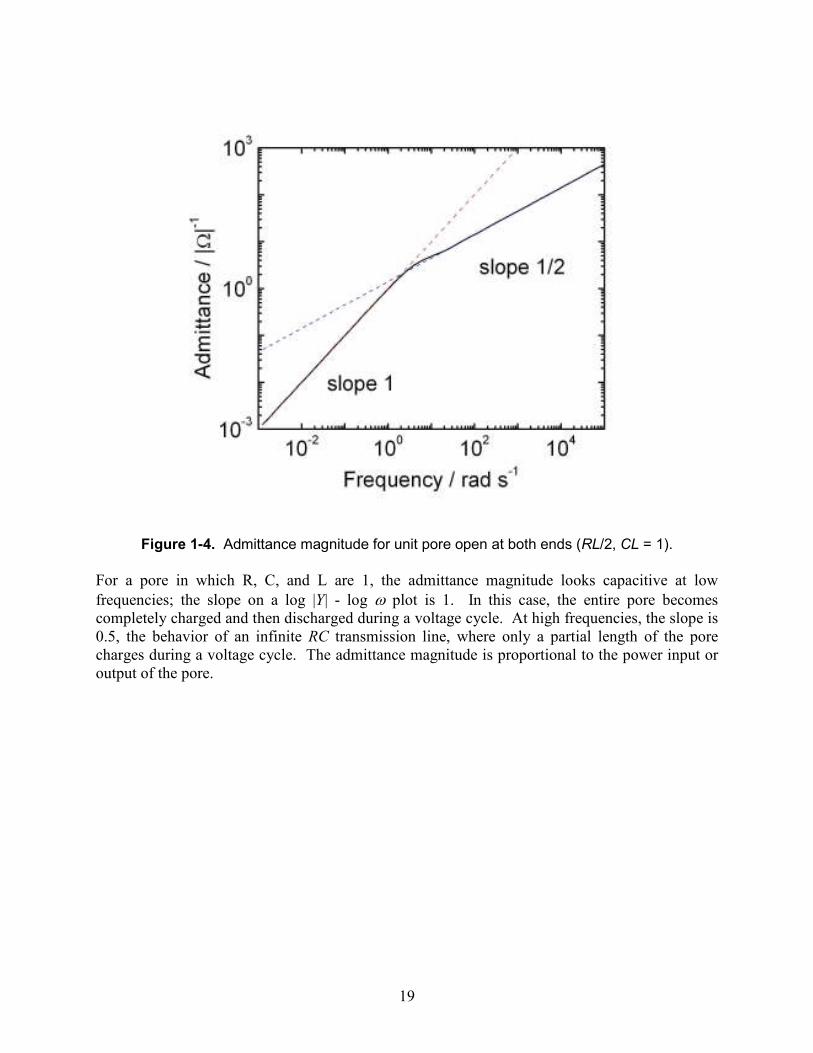
Figure 1-4. Admittance magnitude for unit pore open at both ends (RL/2, CL = 1).
For a pore in which R, C, and L are 1, the admittance magnitude looks capacitive at low frequencies; the slope on a log |Y| - log ω plot is 1. In this case, the entire pore becomes completely charged and then discharged during a voltage cycle. At high frequencies, the slope is 0.5, the behavior of an infinite RC transmission line, where only a partial length of the pore charges during a voltage cycle. The admittance magnitude is proportional to the power input or output of the pore.
20
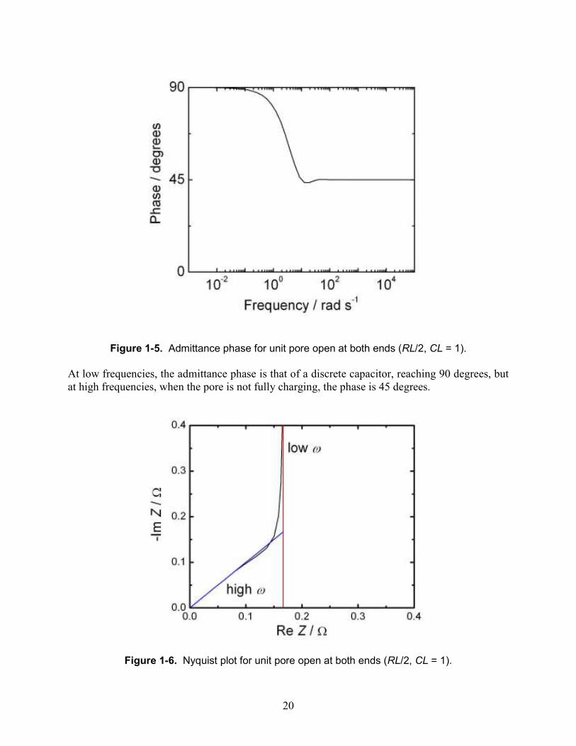
Figure 1-5. Admittance phase for unit pore open at both ends (RL/2, CL = 1).
At low frequencies, the admittance phase is that of a discrete capacitor, reaching 90 degrees, but at high frequencies, when the pore is not fully charging, the phase is 45 degrees.
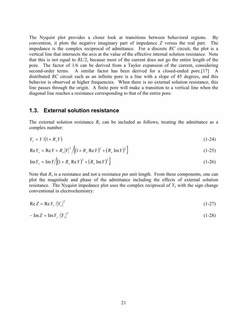
Figure 1-6. Nyquist plot for unit pore open at both ends (RL/2, CL = 1).
21
The Nyquist plot provides a closer look at transitions between behavioral regions. By convention, it plots the negative imaginary part of impedance Z versus the real part. The impedance is the complex reciprocal of admittance. For a discrete RC circuit, the plot is a vertical line that intersects the axis at the value of the effective internal solution resistance. Note that this is not equal to RL/2, because most of the current does not go the entire length of the pore. The factor of 1/6 can be derived from a Taylor expansion of the current, considering second-order terms. A similar factor has been derived for a closed-ended pore.[17] A distributed RC circuit such as an infinite pore is a line with a slope of 45 degrees, and this behavior is observed at higher frequencies. When there is no external solution resistance, this line passes through the origin. A finite pore will make a transition to a vertical line when the diagonal line reaches a resistance corresponding to that of the entire pore.
1.3. External solution resistance The external solution resistance Rx can be included as follows, treating the admittance as a complex number:
( )YRYY xx += 1/ (1-24)
( ) ( )[ ]222ImRe1ReRe YRYRYRYY xxxx +++= (1-25)
( ) ( )[ ]22 ImRe1ImIm YRYRYY xxx ++= (1-26)
Note that Rx is a resistance and not a resistance per unit length. From these components, one can plot the magnitude and phase of the admittance including the effects of external solution resistance. The Nyquist impedance plot uses the complex reciprocal of Yx with the sign change conventional in electrochemistry:
2/ReRe xx YYZ = (1-27)
2/ImIm xx YYZ =− (1-28)
22
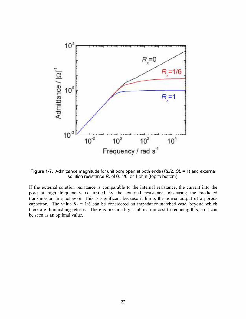
Figure 1-7. Admittance magnitude for unit pore open at both ends (RL/2, CL = 1) and external
solution resistance Rx of 0, 1/6, or 1 ohm (top to bottom).
If the external solution resistance is comparable to the internal resistance, the current into the pore at high frequencies is limited by the external resistance, obscuring the predicted transmission line behavior. This is significant because it limits the power output of a porous capacitor. The value Rx = 1/6 can be considered an impedance-matched case, beyond which there are diminishing returns. There is presumably a fabrication cost to reducing this, so it can be seen as an optimal value.
23
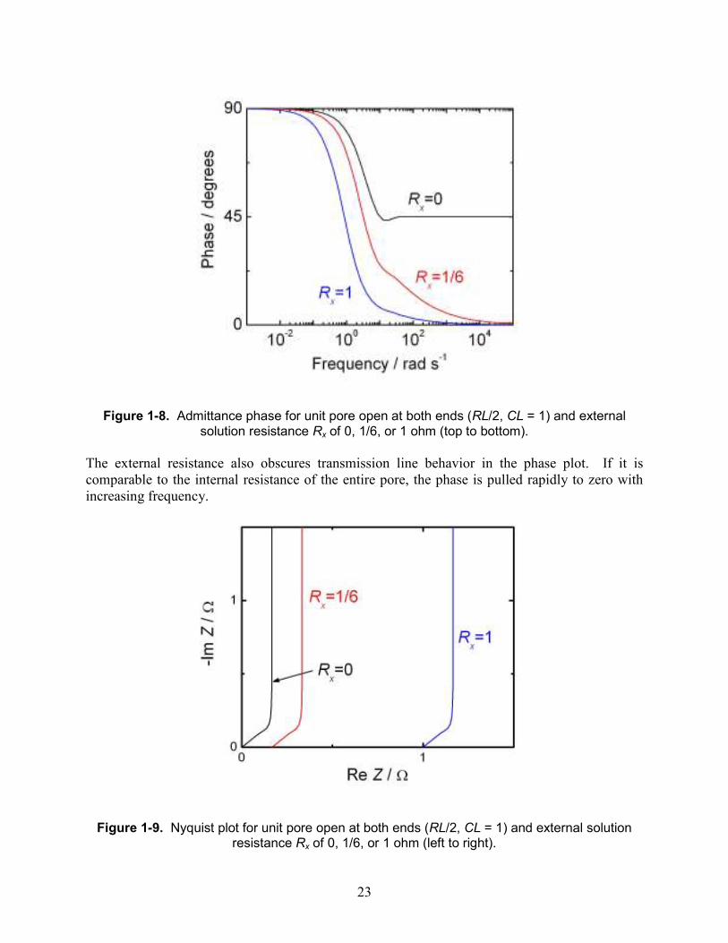
Figure 1-8. Admittance phase for unit pore open at both ends (RL/2, CL = 1) and external solution resistance Rx of 0, 1/6, or 1 ohm (top to bottom).
The external resistance also obscures transmission line behavior in the phase plot. If it is comparable to the internal resistance of the entire pore, the phase is pulled rapidly to zero with increasing frequency.
Figure 1-9. Nyquist plot for unit pore open at both ends (RL/2, CL = 1) and external solution
resistance Rx of 0, 1/6, or 1 ohm (left to right).
24
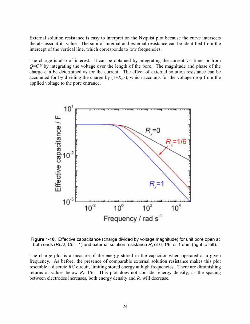
External solution resistance is easy to interpret on the Nyquist plot because the curve intersects the abscissa at its value. The sum of internal and external resistance can be identified from the intercept of the vertical line, which corresponds to low frequencies. The charge is also of interest. It can be obtained by integrating the current vs. time, or from Q=CV by integrating the voltage over the length of the pore. The magnitude and phase of the charge can be determined as for the current. The effect of external solution resistance can be accounted for by dividing the charge by (1+RxY), which accounts for the voltage drop from the applied voltage to the pore entrance.
Figure 1-10. Effective capacitance (charge divided by voltage magnitude) for unit pore open at
both ends (RL/2, CL = 1) and external solution resistance Rx of 0, 1/6, or 1 ohm (right to left).
The charge plot is a measure of the energy stored in the capacitor when operated at a given frequency. As before, the presence of comparable external solution resistance makes this plot resemble a discrete RC circuit, limiting stored energy at high frequencies. There are diminishing returns at values below Rx=1/6. This plot does not consider energy density; as the spacing between electrodes increases, both energy density and Rx will decrease.
25
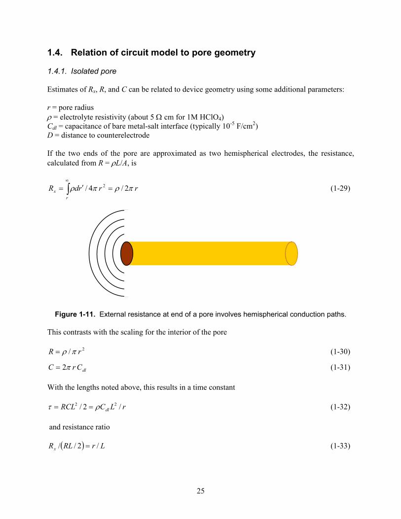
1.4. Relation of circuit model to pore geometry 1.4.1. Isolated pore Estimates of Rx, R, and C can be related to device geometry using some additional parameters: r = pore radius ρ = electrolyte resistivity (about 5 Ω cm for 1M HClO4) Cdl = capacitance of bare metal-salt interface (typically 10-5 F/cm2) D = distance to counterelectrode If the two ends of the pore are approximated as two hemispherical electrodes, the resistance, calculated from R = ρL/A, is
rrrdRr
x πρπρ 2/4/ 2 =′= ∫∞
(1-29)
Figure 1-11. External resistance at end of a pore involves hemispherical conduction paths.
This contrasts with the scaling for the interior of the pore
2/ rR πρ= (1-30)
dlCrC π2= (1-31)
With the lengths noted above, this results in a time constant
rLCRCL dl /2/ 22 ρτ == (1-32)
and resistance ratio
( ) LrRLRx /2// = (1-33)
26
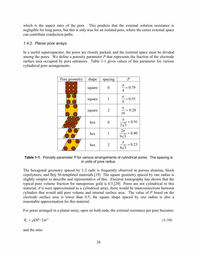
which is the aspect ratio of the pore. This predicts that the external solution resistance is negligible for long pores, but this is only true for an isolated pore, where the entire external space can contribute conduction paths. 1.4.2. Planar pore arrays In a useful supercapacitor, the pores are closely packed, and the external space must be divided among the pores. We define a porosity parameter P that represents the fraction of the electrode surface area occupied by pore entrances. Table 1-1 gives values of this parameter for various cylindrical pore arrangements.
Pore geometry shape spacing P
square 0 79.0
4=
π
square 1 35.0
9=
π
square 2 20.0
16=
π
hex 0 91.0
32=
π
hex 1 40.0
39
2=
π
hex 2 23.0
38=
π
Table 1-1. Porosity parameter P for various arrangements of cylindrical pores. The spacing is
in units of pore radius.
The hexagonal geometry spaced by 1-2 radii is frequently observed in porous alumina, block copolymers, and Brij 56-templated materials.[19] The square geometry spaced by one radius is slightly simpler to describe and representative of this. Electron tomography has shown that the typical pore volume fraction for nanoporous gold is 0.5.[20] Pores are not cylindrical in this material; if it were approximated as a cylindrical array, there would be interconnections between cylinders that would add pore volume and internal surface area. The value of P based on the electrode surface area is lower than 0.5; the square shape spaced by one radius is also a reasonable approximation for this material. For pores arranged in a planar array, open on both ends, the external resistance per pore becomes
22/ rDPRx πρ= (1-34)
and the ratio
27
( ) LDPRLRx /2// = (1-35)
The ratio of D/L needed to obtain the optimal ratio of 1/6 is 1/2P. Because P is commonly about 0.35, this value is about 1.4 for many materials.
Figure 1-12. External resistance at end of close-packed pores involves confined conduction
paths.
In this case, the counterelectrode must be at a distance less than the pore depth if the external resistance is to be negligible. 1.4.3. Cylindrical pore arrays The strong distance dependence for the planar array can be alleviated slightly by use of a cylindrical geometry, where one dimension of the external conductance path expands radially. If
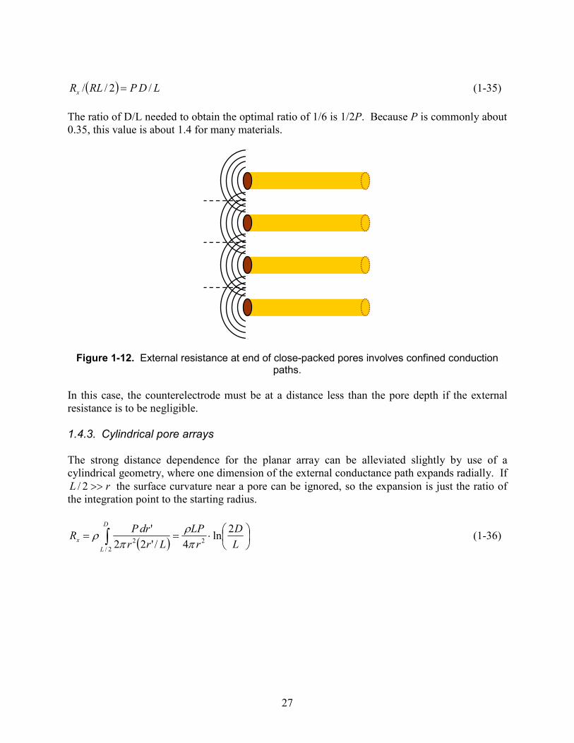
rL >>2/ the surface curvature near a pore can be ignored, so the expansion is just the ratio of the integration point to the starting radius.
( )
⋅== ∫ L
D
r
LP
Lrr
drPR
D
L
x
2ln
4/'22
'2
2/2 π
ρπ
ρ (1-36)
28
Figure 1-13. External resistance at cylindrically packed pores involves confined conduction
paths that expand in one dimension.
We will ignore the question of how curvature is accommodated at points deeper in the wire, where the pores intersect. The primary impact of cylindrical geometry is how the electrode communicates to the counterelectrode; we do not expect a strong effect on whether the electrode has a circular, square, or other cross section. In this case, the ratio of external to internal resistance for a cylindrical pore in a wire electrode is:
( ) ( ) ( )LDPRLRx /2ln2/2// = (1-37)
The optimal D/L is about 1.3 with the assumptions above. This assumes a concentric counterelectrode that should have a comparable capacitance. The main advantage of the cylindrical geometry is that the behavior of an electrochemical cell is relatively insensitive to the distance between the electrodes, which is convenient for testing purposes.
1.5. Implications for supercapacitor design For actual device design, it is clear that the target should be layered or interdigitated porous electrodes where the interelectrode spacing is comparable to, and preferably less than half of, the pore depth, or usually equivalently the thickness of each electrode. This will achieve the optimal power and energy density for a given geometry. Fabrication of the electrodes and ion-conducting separator in of such dimensions are each probably similarly difficult, so this arrangement is likely to be economically optimal as well.
29
Choice of remaining properties depends on tuning to the desired capacitance per unit area (obtained by multiplying capacitance per pore by pores per unit area) and effective time constant, accounting for the factor of 6 discussed above.
rLCPC dlarea /2= (1-38)
PLCrLC areadleff 12/6/2 ρρτ == (1-39)
given design parameters and practical constraints. Other bulk design parameters include capacitance per unit volume, obtained by dividing Carea by L, and the internal and external resistances for planar and cylindrical electrodes for a unit surface area, obtained by multiplying those values by area per pore. For design purposes, the factor of 6 is included in the internal resistance here.
rCPC dlvol /2= (1-40)
PLRarea 12/ρ= (1-41)
Planar 2/, DR areax ρ= (1-42)
For a wire electrode, the diameter is L, and we can obtain values per unit length. Capacitance per unit length Clength is the product of the wire’s cross-sectional area and Cvol. Rx and Rcyl are multiplied by the surface area per pore and divided by half the circumference (because they already account for two ends of each pore). Cylindrical PRlength πρ /= (1-43)
Cylindrical ( ) ( )LDR lengthx 2ln2/, πρ= (1-44)
Cylindrical rCLPC dllength 2/2π= (1-45)
Cylindrical rLCdleff 12/2ρτ = (1-46)
It would be hard to find an ion conductor with a resistivity lower than a strong aqueous acid near 1M, so this can be taken as a physical constraint for most purposes. A related constraint is the finite conductivity of the electrode, which we have neglected so far. For a metal electrode, this is generally a factor of about 106 higher than the ion conductor. The total interfacial area of the capacitor should not exceed the cross-sectional area of the contacts to the device by more than this factor. This does not necessarily place an upper boundary on stored energy; the devices can be arranged in a series configuration that is in close contact, which increases the operating voltage while decreasing the capacitance. Because stored energy is ½CV2, placing two equal capacitors in series doubles the stored energy. This also halves the time constant. The tradeoffs associated with changing operating voltage that were discussed earlier must be considered. Creating a higher Cdl than those ions on a bare noble metal surface is also difficult without invoking redox reactions, which are a promising area of study but beyond the scope of this work.
30
The chemical reaction rates can limit charging times, and often multiphase mass transport processes are involved. It always pays to make pores smaller until nanoscale phenomena cause the model presented here to break down; that topic will be discussed later in this report. It is then beneficial to make L, the length scale of the electrode (and their interpenetration) as small as practical. This analysis tells us that there is a premium on development methods for electrode materials with both pores and interpenetration on as small a scale as possible. This topic will also be explored later in this report. In the next chapter, we compare these performance and scaling predictions with experiment.
31
2. NANOPOROUS GOLD AS A TEST PLATFORM FOR SUPERCAPACITOR DESIGN
Experiments presented here were performed primarily by Chung-An Max Wu, with contributions
from Ben Jacobs. Markus Ong and Bonnie Pierson contributed to optimization and validation of
the electrode fabrication procedure.
2.1. Introduction Many state-of-art capacitors employ the use of porous materials. These include electrolytic capacitors, which have micrometer-scale pores with thick oxides in contact with a liquid electrolyte. The electrolyte in this case serves not to produce small dielectric spacing but to limit dielectric breakdown and its consequences to an electrical circuit.[21] Commercial supercapacitors usually rely on porous carbon, often coated with metal oxides to increase the energy density by adding reversible redox charge storage. The combination of porous conductor and electrolyte found in supercapacitors forms an electrochemical double-layer, in which electrons from the conductor and ions from the electrolyte accumulate at the electrode/electrolyte interface under applied voltage.[1, 22] With the high surface area offered by porous electrodes, this allows more charge carriers to be packed into a smaller volume. While capacitors made from them can be profitably manufactured to meet certain quality specifications, porous carbon electrodes are difficult to study and optimize. In particular, it is difficult to precisely control the conductivity, surface uniformity, and pore architecture of porous carbon. Unless it is formed at well over 1000 °C, porous carbon is more amorphous than graphitic, and its conductivity is significantly lower. Furthermore, physical imperfections in the graphitic structure may chemically react with the surrounding electrolyte, further reducing performance and reliability. [22] To gain a clear understanding of porous electrode charging behavior with experimental backing, and in particular of nanoporous electrodes, we have sought a simple, well defined nanoporous electrode platform on which the assertions of the previous chapter can be verified. Our long-term strategy is to apply information gained from this system clarify the behavior of materials that are more physically complex, but more economical for large-scale production. Gold is an ideal material for this purpose because it has a high conductivity, a surface that is relatively chemically stable, and decades of prior detailed study into its behavior.[23-30] Its chemical stability allows use of a wide range of potentials and electrolytes, and its surface can be chemically modified with alkanethiol monolayers to produce diverse functionality and tune capacitance.[31-34] Nanoporous gold can be formed by oxidatively stripping silver from a silver-gold alloy either in concentrated (15 M) nitric acid [biener nl6] or by electrochemical etching in 1 M nitric acid.[35] The pores in this material are interconnected and in the 10-20 nm diameter range. They can be hundreds of micrometers deep. This pore diameter is much larger than that achievable in carbon [36] or platinum group metals [37, 38] but this material’s pores have sufficient and consistent aspect ratio to test design principles derived in the previous chapter. In pores smaller than 10 nm, mass transport limitations become severe, especially as effects of finite ion and solvent size become important,[39-42] so models must be more
32
complicated. Pore structure at this size scale can be easily verified by scanning electron microscopy. For gold, achieving smaller pores is difficult, because the metal is relatively prone to sintering.[43] Preliminary electrochemical characterization has already been performed on nanoporous gold films and foils. [35, 44] Dealloyed nanoporous gold is thus an ideal platform for testing the limits of the concepts pioneered by de Levie. In this work, we evaluate our model of porous electrode behavior using nanoporous gold wires, a form factor that is easy to fabricate and is predicted to have well defined external solution resistance. We demonstrate that the model is accurate over a significant range of parameter space, and that we can tune the ratio of internal to external resistance using alkanethiol monolayers, which most likely is caused by salt partitioning out of pores, an interesting and important physical effect. We also observe breakdown of the model at low salt concentrations, which will be addressed in a subsequent chapter. Experimental validation of our model will provide confidence in our efforts to optimize supercapacitor design.
2.2. Experimental Methods 2.2.1. Electrode material A 2 cm length of silver-gold alloy wire, 0.2 mm in diameter, was cut from a spool obtained from Refining Systems Inc. (Las Vegas, NV). The alloy is 50:50 by weight, or 2:1 Ag:Au by atoms. To structurally stabilize AuAg wires in preparation for etching, 4 cm gold wire, 0.127 mm diameter. The braided wires were annealed together in N2 at 650°C overnight. Wires that were not annealed were more likely to crack after etching. 2.2.2. Dealloying to form nanoporous gold Alloy electrodes were etched in a three-electrode cell with a gold counterelectrode and silver reference electrode. The electrodes were immersed in an aqueous solution of 1M HNO3 along with 10mM AgNO3 to stabilize the reference electrode at the beginning of the process. Etching was performed using a computer-controlled PAR 273 potentiostat. A voltammogram between +500 and 1200 mV versus the reference electrode was performed to verify onset of etching current above 1000 mV. The wire was then etched for 30 min at 1200 mV, monitoring the amount of charge passed using the potentiostat’s integration circuit. The alloy wire segment became black, and a large volume of silver plated onto the counterelectrode. After etching, wires were soaked in deionized water for two minutes, and then the electrolyte to be used for at least two minutes. In an alternative procedure, a wire is soaked overnight in 8-15 M nitric acid for several hours or overnight. To minimize heat of mixing, the wire is soaked for several minutes in intermediate concentrations of nitric acid (0.5-8 M) before the deionized water soak. 2.2.3. Electrochemical characterization To characterize the etched wires, the porous gold wires were suspended in a three-electrode cell made from a 25 mL beaker with a platinum gauze counter electrode spanning most of the inner
33
circumference of the beaker. Electrolytes studied include 1M HClO4 in which case a Ag/AgClO4/1M HClO4 reference electrode was used, and 1M tetramethylammonium lactate, which used a Ag/AgCl/1M KCl reference electrode. Two electroanalytic procedures were performed: cyclic voltammetry (CV) and frequency response (impedance spectroscopy). Frequency response was measured using the PAR 273 potentiostat and a SRS 785 dynamic signal analyzer, while the CVs were measured with the potentiostat driven by its internal waveform generator or a Wavetek 395. Ranges of capacitive behavior were verified by cyclic voltammetry prior to frequency response measurements. 2.2.4. Monolayer formation Alkanethiol monolayers were formed through spontaneous adsorption of 6-mercapto-1-hexanol and other alkanethiols obtained from Aldrich. After etching or initial characterization, a porous gold electrode was soaked for 1 minute in deionized H2O followed by a 2 minute soak in ethanol before immersion in a fresh 4 mL solution of 100 mM alkanethiol in ethanol [33, 45] After soaking for at least 24 hours, the wires were then removed and soaked in ethanol and water to remove residual adsorbate: 2 rinses in ethanol for 5 minutes each, then another 5 minute soak in water.
2.3. Data Analysis Methods 2.3.1. Cyclic Voltammetry A capacitive region was determined for each electrode by cyclic voltammetry. For a discrete RC circuit, at low scan rates, where IR drop is negligible, a voltage ramp results in a constant current, as determined by the time derivative of the definition of capacitance Q=CV:
dt
dVCI =
The forward and reverse scans of the voltammogram result in horizontal lines on opposite sides of I = 0. In a real electrochemical system, capacitance can be nonlinear due to potential-dependent reconfiguration of the ions in the double layer, and redox reactions such as solvent, salt, or surface oxidation cause deviations from capacitive behavior at potential extremes and sometimes intermediate applied potentials. 2.3.2. Frequency response (impedance spectroscopy) An SRS SR785 frequency response analyzer generated a chirp signal (sinusoidal voltage with increasing frequency) with an amplitude and bias determined by cyclic voltammetry, typically 500 mV amplitude with zero bias. The response and a reference signal are sampled and processed at several points across an 8 mHz – 102 kHz range to calculate the admittance magnitude, phase, and real and imaginary components. Conceptually, we consider a voltage input wave applied to the cell in the form of )sin( tA ω⋅ , where A is the amplitude and ω is the
frequency of the wave; and the current response from the cell, scaled and converted into a
34
voltage wave in the form of )sin( φω +⋅ tD . The instrument also generates values of the
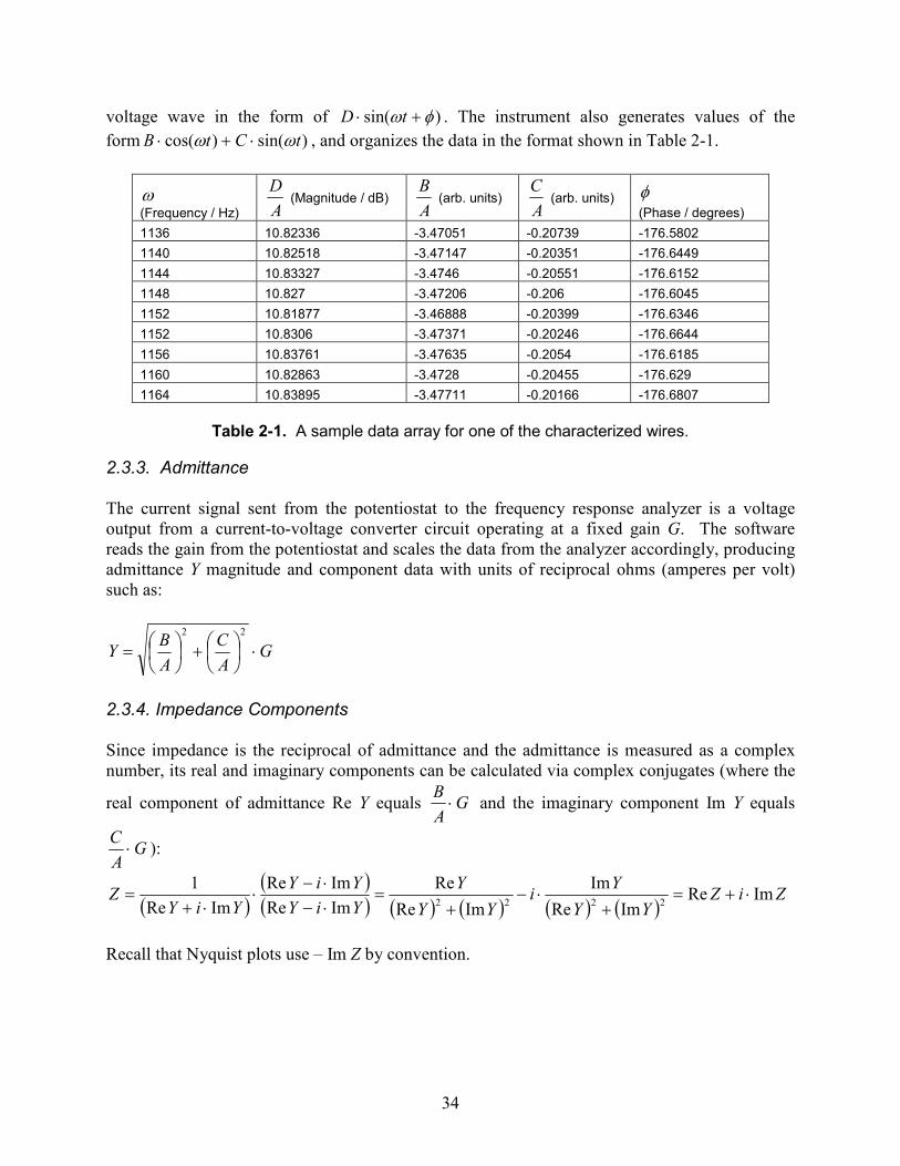
form )sin()cos( tCtB ωω ⋅+⋅ , and organizes the data in the format shown in Table 2-1.
ω
(Frequency / Hz) A
D (Magnitude / dB)
A
B (arb. units)
A
C (arb. units) φ
(Phase / degrees)
1136 10.82336 -3.47051 -0.20739 -176.5802
1140 10.82518 -3.47147 -0.20351 -176.6449
1144 10.83327 -3.4746 -0.20551 -176.6152
1148 10.827 -3.47206 -0.206 -176.6045
1152 10.81877 -3.46888 -0.20399 -176.6346
1152 10.8306 -3.47371 -0.20246 -176.6644
1156 10.83761 -3.47635 -0.2054 -176.6185
1160 10.82863 -3.4728 -0.20455 -176.629
1164 10.83895 -3.47711 -0.20166 -176.6807
Table 2-1. A sample data array for one of the characterized wires.
2.3.3. Admittance The current signal sent from the potentiostat to the frequency response analyzer is a voltage output from a current-to-voltage converter circuit operating at a fixed gain G. The software reads the gain from the potentiostat and scales the data from the analyzer accordingly, producing admittance Y magnitude and component data with units of reciprocal ohms (amperes per volt) such as:
GA
C
A
BY ⋅
+
=22
2.3.4. Impedance Components Since impedance is the reciprocal of admittance and the admittance is measured as a complex number, its real and imaginary components can be calculated via complex conjugates (where the
real component of admittance Re Y equals GA
B⋅ and the imaginary component Im Y equals
GA
C⋅ ):
( )( )( ) ( ) ( ) ( ) ( )
ZiZYY
Yi
YY
Y
YiY
YiY
YiYZ ImRe
ImRe
Im
ImRe
Re
ImRe
ImRe
ImRe
12222
⋅+=+
⋅−+
=⋅−⋅−
⋅⋅+
=
Recall that Nyquist plots use – Im Z by convention.
35
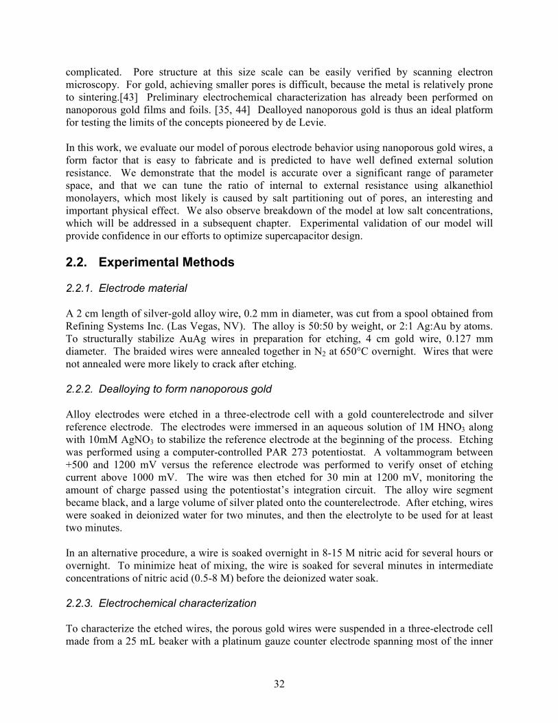
2.4. Results 2.4.1. Etching of wires The etching process results in uniform pores throughout the wire, as shown in Figure 2-1. This wire was etched in concentrated nitric acid. The submicron texture seen here is consistent with literature reports, with pores in the 20 nm range. We observed smaller pores and higher capacitance (closer to 10 nm) by the electrochemical etch.
Figure 2-1. Etched porous gold wire.
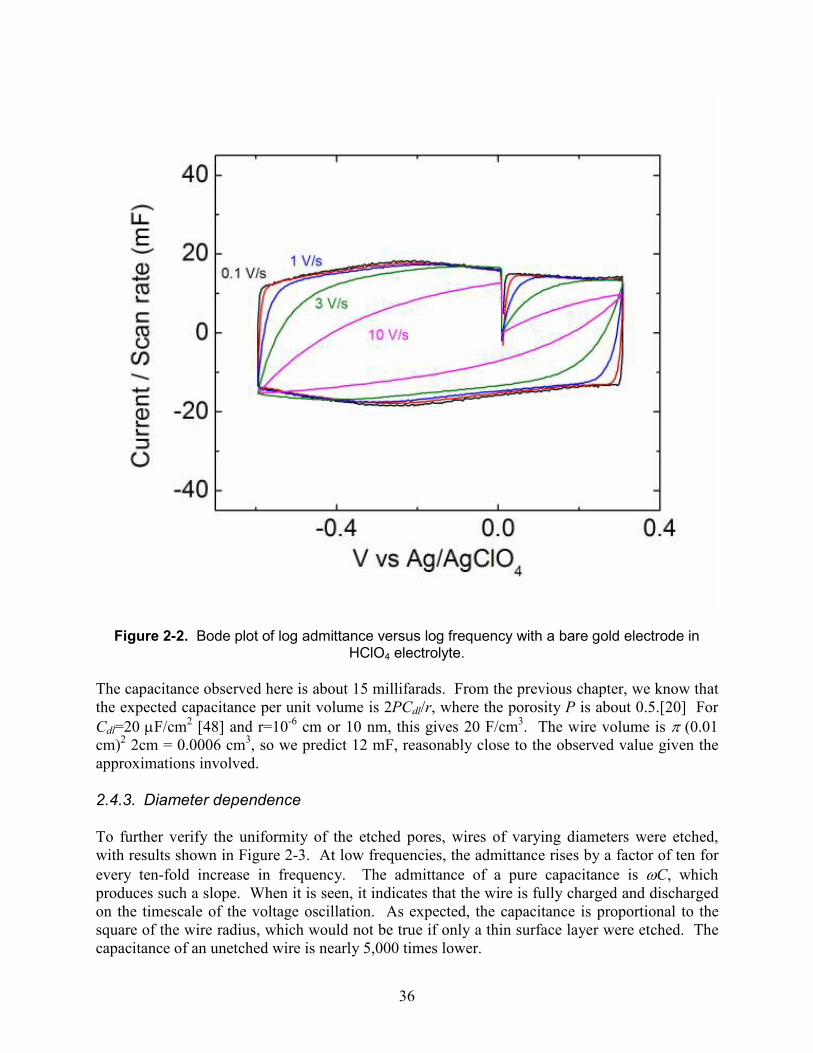
2.4.2. Cyclic voltammetry in perchloric acid Perchloric acid solutions are useful as electrolytes with gold electrodes because the anion interacts weakly with the surface, undergoing relatively little specific adsorption, which can result in nonlinearities in the capacitance.[29, 46, 47] At concentrations near 1 M, it is among the highest conductivity electrolytes known, with values near 0.2 S/cm. Ammonium and alkali metal salts are generally at least fivefold less conductive. This means that experiments can be performed more quickly, at higher scan rates or frequencies. Before measuring the frequency response of an electrode, it was characterized by cyclic voltammetry to establish a voltage window in which the electrode is capacitive. Figure 2-2 shows measurements of this window for a porous 0.2 mm wire. At scan rates above 1 V/s, the wire does not fully charge on the timescale of the experiment, and takes on a leaf-like appearance, a common observation with porous electrodes. At low scan rates, the wire is fully charged well before the potential scan changes direction, and it is possible to derive the capacitance from the voltammogram.
36
Figure 2-2. Bode plot of log admittance versus log frequency with a bare gold electrode in HClO4 electrolyte.
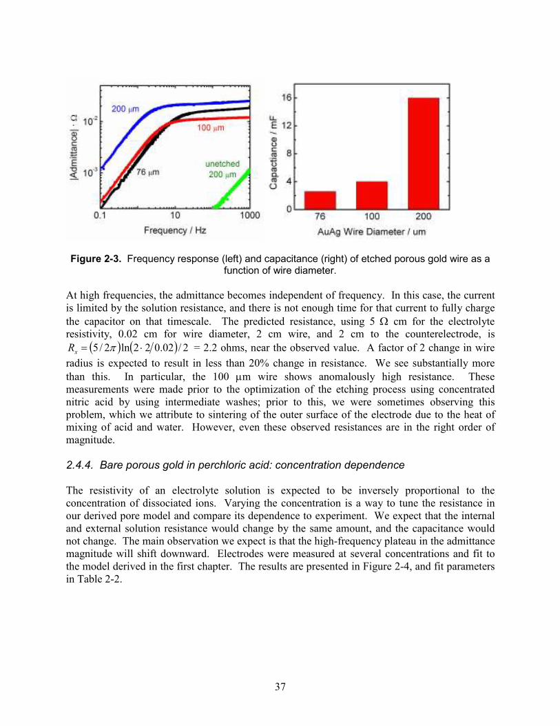
The capacitance observed here is about 15 millifarads. From the previous chapter, we know that the expected capacitance per unit volume is 2PCdl/r, where the porosity P is about 0.5.[20] For Cdl=20 µF/cm2 [48] and r=10-6 cm or 10 nm, this gives 20 F/cm3. The wire volume is π (0.01 cm)2 2cm = 0.0006 cm3, so we predict 12 mF, reasonably close to the observed value given the approximations involved. 2.4.3. Diameter dependence To further verify the uniformity of the etched pores, wires of varying diameters were etched, with results shown in Figure 2-3. At low frequencies, the admittance rises by a factor of ten for every ten-fold increase in frequency. The admittance of a pure capacitance is ωC, which produces such a slope. When it is seen, it indicates that the wire is fully charged and discharged on the timescale of the voltage oscillation. As expected, the capacitance is proportional to the square of the wire radius, which would not be true if only a thin surface layer were etched. The capacitance of an unetched wire is nearly 5,000 times lower.
37
Figure 2-3. Frequency response (left) and capacitance (right) of etched porous gold wire as a
function of wire diameter.
At high frequencies, the admittance becomes independent of frequency. In this case, the current is limited by the solution resistance, and there is not enough time for that current to fully charge the capacitor on that timescale. The predicted resistance, using 5 Ω cm for the electrolyte resistivity, 0.02 cm for wire diameter, 2 cm wire, and 2 cm to the counterelectrode, is
( ) ( ) 2/02.022ln2/5 ⋅= πxR = 2.2 ohms, near the observed value. A factor of 2 change in wire
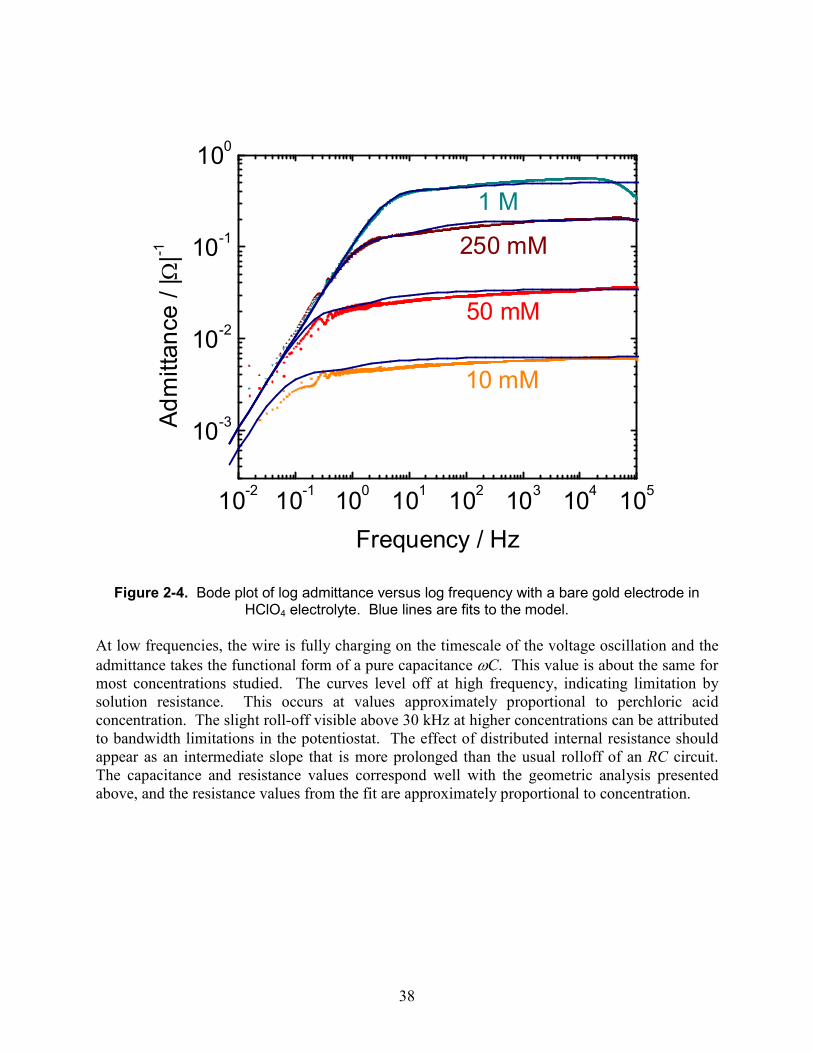
radius is expected to result in less than 20% change in resistance. We see substantially more than this. In particular, the 100 µm wire shows anomalously high resistance. These measurements were made prior to the optimization of the etching process using concentrated nitric acid by using intermediate washes; prior to this, we were sometimes observing this problem, which we attribute to sintering of the outer surface of the electrode due to the heat of mixing of acid and water. However, even these observed resistances are in the right order of magnitude. 2.4.4. Bare porous gold in perchloric acid: concentration dependence The resistivity of an electrolyte solution is expected to be inversely proportional to the concentration of dissociated ions. Varying the concentration is a way to tune the resistance in our derived pore model and compare its dependence to experiment. We expect that the internal and external solution resistance would change by the same amount, and the capacitance would not change. The main observation we expect is that the high-frequency plateau in the admittance magnitude will shift downward. Electrodes were measured at several concentrations and fit to the model derived in the first chapter. The results are presented in Figure 2-4, and fit parameters in Table 2-2.
38
10-2
10-1
100
101
102
103
104
105
10-3
10-2
10-1
100
Ad
mitta
nce
/ |Ω
|-1
Frequency / Hz
1 M
250 mM
50 mM
10 mM
Figure 2-4. Bode plot of log admittance versus log frequency with a bare gold electrode in
HClO4 electrolyte. Blue lines are fits to the model.
At low frequencies, the wire is fully charging on the timescale of the voltage oscillation and the admittance takes the functional form of a pure capacitance ωC. This value is about the same for most concentrations studied. The curves level off at high frequency, indicating limitation by solution resistance. This occurs at values approximately proportional to perchloric acid concentration. The slight roll-off visible above 30 kHz at higher concentrations can be attributed to bandwidth limitations in the potentiostat. The effect of distributed internal resistance should appear as an intermediate slope that is more prolonged than the usual rolloff of an RC circuit. The capacitance and resistance values correspond well with the geometric analysis presented above, and the resistance values from the fit are approximately proportional to concentration.
39
0 4 8 12 16 200
4
8
12
16
20
Im
(Z)
/ O
hm
Re(Z) / Ohm
1 M
500 mM
250 mM
100 mM
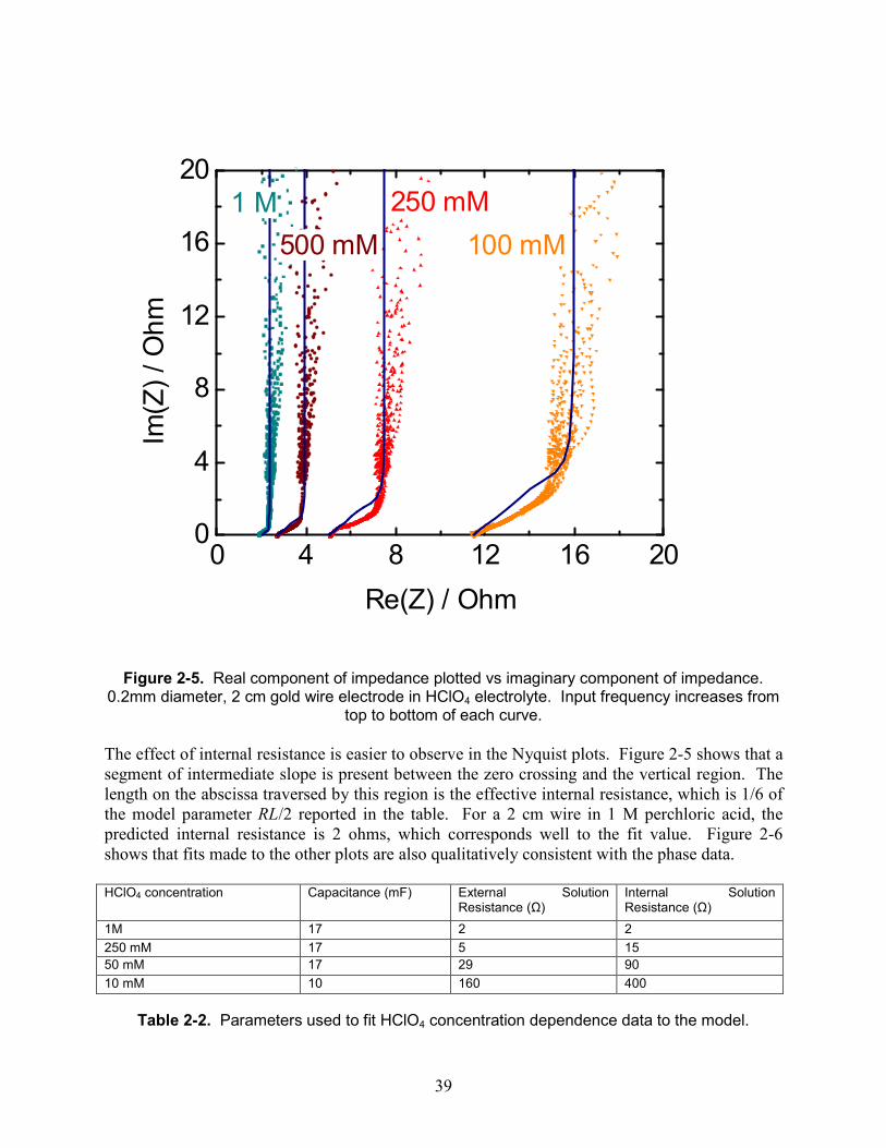
Figure 2-5. Real component of impedance plotted vs imaginary component of impedance. 0.2mm diameter, 2 cm gold wire electrode in HClO4 electrolyte. Input frequency increases from
top to bottom of each curve.
The effect of internal resistance is easier to observe in the Nyquist plots. Figure 2-5 shows that a segment of intermediate slope is present between the zero crossing and the vertical region. The length on the abscissa traversed by this region is the effective internal resistance, which is 1/6 of the model parameter RL/2 reported in the table. For a 2 cm wire in 1 M perchloric acid, the predicted internal resistance is 2 ohms, which corresponds well to the fit value. Figure 2-6 shows that fits made to the other plots are also qualitatively consistent with the phase data. HClO4 concentration Capacitance (mF) External Solution
Resistance (Ω) Internal Solution Resistance (Ω)
1M 17 2 2
250 mM 17 5 15
50 mM 17 29 90
10 mM 10 160 400
Table 2-2. Parameters used to fit HClO4 concentration dependence data to the model.
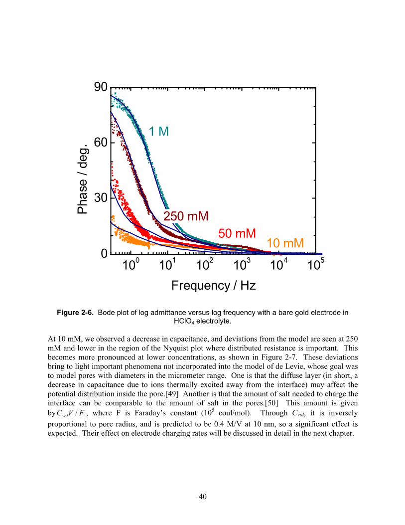
40
100
101
102
103
104
105
0
30
60
90
10 mM50 mM
250 mM
P
ha
se / d
eg
.
Frequency / Hz
1 M
Figure 2-6. Bode plot of log admittance versus log frequency with a bare gold electrode in
HClO4 electrolyte.
At 10 mM, we observed a decrease in capacitance, and deviations from the model are seen at 250 mM and lower in the region of the Nyquist plot where distributed resistance is important. This becomes more pronounced at lower concentrations, as shown in Figure 2-7. These deviations bring to light important phenomena not incorporated into the model of de Levie, whose goal was to model pores with diameters in the micrometer range. One is that the diffuse layer (in short, a decrease in capacitance due to ions thermally excited away from the interface) may affect the potential distribution inside the pore.[49] Another is that the amount of salt needed to charge the interface can be comparable to the amount of salt in the pores.[50] This amount is given by FVCvol / , where F is Faraday’s constant (105 coul/mol). Through Cvol, it is inversely
proportional to pore radius, and is predicted to be 0.4 M/V at 10 nm, so a significant effect is expected. Their effect on electrode charging rates will be discussed in detail in the next chapter.
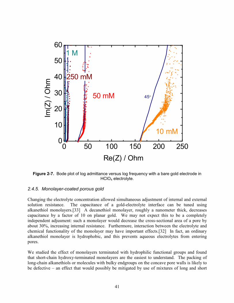
41
0 50 100 150 200 2500
10
20
30
40
50
60
Im(Z
) / O
hm
Re(Z) / Ohm
1 M
250 mM
50 mM
10 mM
45°
Figure 2-7. Bode plot of log admittance versus log frequency with a bare gold electrode in
HClO4 electrolyte.
2.4.5. Monolayer-coated porous gold Changing the electrolyte concentration allowed simultaneous adjustment of internal and external solution resistance. The capacitance of a gold-electrolyte interface can be tuned using alkanethiol monolayers.[33] A decanethiol monolayer, roughly a nanometer thick, decreases capacitance by a factor of 10 on planar gold. We may not expect this to be a completely independent adjusment: such a monolayer would decrease the cross-sectional area of a pore by about 30%, increasing internal resistance. Furthermore, interaction between the electrolyte and chemical functionality of the monolayer may have important effects.[32] In fact, an ordinary alkanethiol monolayer is hydrophobic, and this prevents aqueous electrolytes from entering pores. We studied the effect of monolayers terminated with hydrophilic functional groups and found that short-chain hydroxy-terminated monolayers are the easiest to understand. The packing of long-chain alkanethiols or molecules with bulky endgroups on the concave pore walls is likely to be defective – an effect that would possibly be mitigated by use of mixtures of long and short
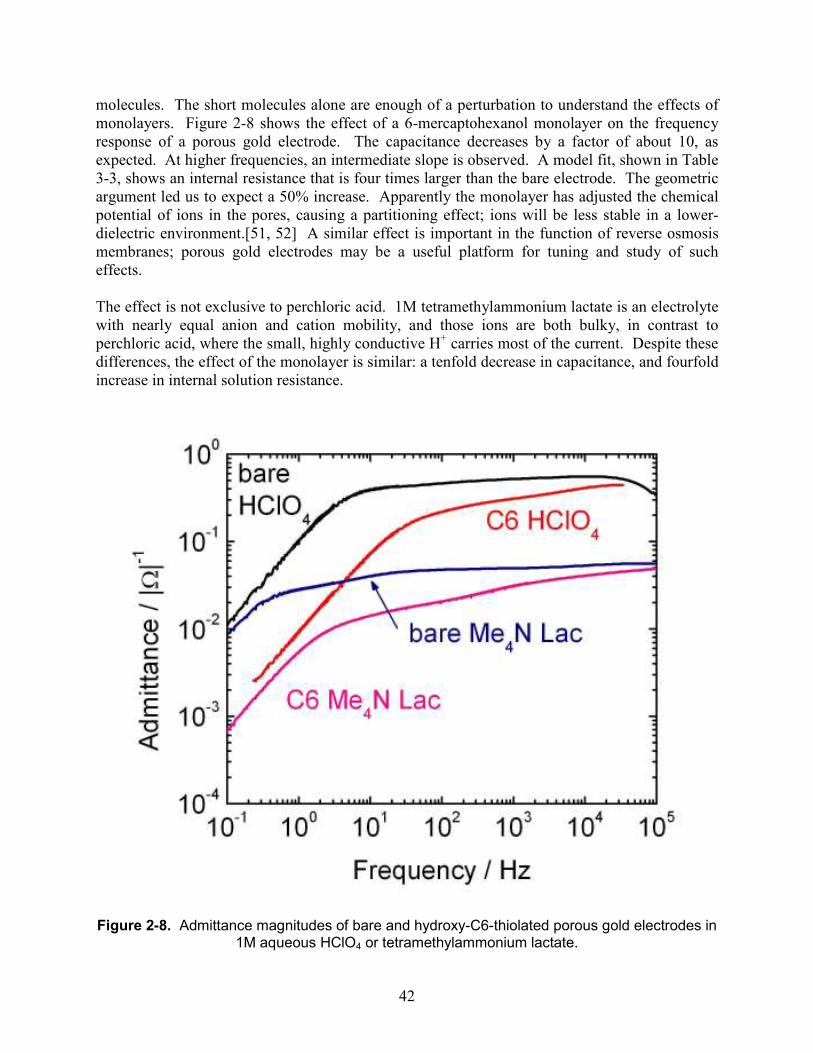
42
molecules. The short molecules alone are enough of a perturbation to understand the effects of monolayers. Figure 2-8 shows the effect of a 6-mercaptohexanol monolayer on the frequency response of a porous gold electrode. The capacitance decreases by a factor of about 10, as expected. At higher frequencies, an intermediate slope is observed. A model fit, shown in Table 3-3, shows an internal resistance that is four times larger than the bare electrode. The geometric argument led us to expect a 50% increase. Apparently the monolayer has adjusted the chemical potential of ions in the pores, causing a partitioning effect; ions will be less stable in a lower-dielectric environment.[51, 52] A similar effect is important in the function of reverse osmosis membranes; porous gold electrodes may be a useful platform for tuning and study of such effects. The effect is not exclusive to perchloric acid. 1M tetramethylammonium lactate is an electrolyte with nearly equal anion and cation mobility, and those ions are both bulky, in contrast to perchloric acid, where the small, highly conductive H+ carries most of the current. Despite these differences, the effect of the monolayer is similar: a tenfold decrease in capacitance, and fourfold increase in internal solution resistance.
Figure 2-8. Admittance magnitudes of bare and hydroxy-C6-thiolated porous gold electrodes in
1M aqueous HClO4 or tetramethylammonium lactate.
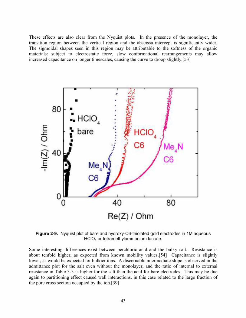
43
These effects are also clear from the Nyquist plots. In the presence of the monolayer, the transition region between the vertical region and the abscissa intercept is significantly wider. The sigmoidal shapes seen in this region may be attributable to the softness of the organic materials: subject to electrostatic force, slow conformational rearrangements may allow increased capacitance on longer timescales, causing the curve to droop slightly.[53]
Figure 2-9. Nyquist plot of bare and hydroxy-C6-thiolated gold electrodes in 1M aqueous
HClO4 or tetramethylammonium lactate.
Some interesting differences exist between perchloric acid and the bulky salt. Resistance is about tenfold higher, as expected from known mobility values.[54] Capacitance is slightly lower, as would be expected for bulkier ions. A discernable intermediate slope is observed in the admittance plot for the salt even without the monolayer, and the ratio of internal to external resistance in Table 3-3 is higher for the salt than the acid for bare electrodes. This may be due again to partitioning effect caused wall interactions, in this case related to the large fraction of the pore cross section occupied by the ion.[39]
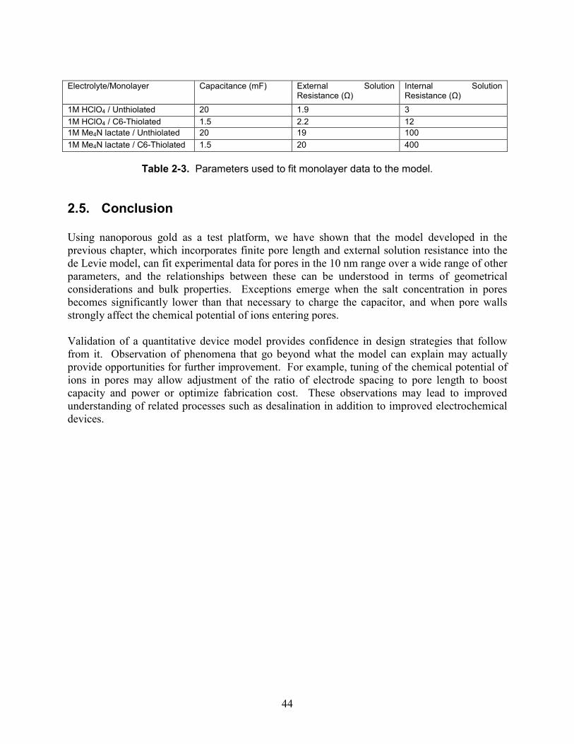
44
Electrolyte/Monolayer Capacitance (mF) External Solution
Resistance (Ω) Internal Solution Resistance (Ω)
1M HClO4 / Unthiolated 20 1.9 3
1M HClO4 / C6-Thiolated 1.5 2.2 12
1M Me4N lactate / Unthiolated 20 19 100
1M Me4N lactate / C6-Thiolated 1.5 20 400
Table 2-3. Parameters used to fit monolayer data to the model.
2.5. Conclusion Using nanoporous gold as a test platform, we have shown that the model developed in the previous chapter, which incorporates finite pore length and external solution resistance into the de Levie model, can fit experimental data for pores in the 10 nm range over a wide range of other parameters, and the relationships between these can be understood in terms of geometrical considerations and bulk properties. Exceptions emerge when the salt concentration in pores becomes significantly lower than that necessary to charge the capacitor, and when pore walls strongly affect the chemical potential of ions entering pores. Validation of a quantitative device model provides confidence in design strategies that follow from it. Observation of phenomena that go beyond what the model can explain may actually provide opportunities for further improvement. For example, tuning of the chemical potential of ions in pores may allow adjustment of the ratio of electrode spacing to pore length to boost capacity and power or optimize fabrication cost. These observations may lead to improved understanding of related processes such as desalination in addition to improved electrochemical devices.
45
3. EFFECT OF SALT DEPLETION ON CHARGING DYNAMICS IN NANOPOROUS ELECTRODES
3.0. Abstract Double-layer supercapacitors built from nanoporous electrodes can have such a high ratio of electrode surface area to pore volume that charging the capacitor can deplete the salt from the liquid volume. This can result in increased resistance, resulting in a slow, nonlinear charging rate. In some cases, this effect is masked by external solution resistance or by transport of salt into the pore from an external reservoir. However, in forms relevant to a compact energy storage device, the phenomenon can have an important effect on charging time and linearity. It can be mitigated through attention to those masking effects and to the symmetry of ion mobilities. We have observed salt depletion effects using dealloyed gold, which has well-defined 10 nm pores and a chemically well understood surface, and by minimizing the salt reservoir. Good correspondence is observed with a modified de Levie model that accounts for reduced conductivity due to salt depletion.
3.1. Introduction 3.1.1. Background
Electrochemical double-layer supercapacitors (EDLCs) achieve very high capacitances per unit volume by adopting the high surface area A of nanoporous materials along with the use of electrolytes, whose ions can penetrate very small pores and achieve atomic-scale effective dielectric thicknesses d.[1, 22] Capacitance is proportional to A/d, stored energy is proportional to CV2, so this leads to high stored energy at a given voltage. One drawback is that the chemical stability of ions limits the applied voltage, so such supercapacitors are best used in low-voltage applications. Another high price paid for this high capacitance is that ion transport through an electrode’s long, narrow pores can be slow compared to the charging times of capacitors made from metal electrodes separated by a solid dielectric. Our goal is to thoroughly understand this kinetic limitation to better understand how to maximize the power that these devices can accept or deliver. Useful models of porous electrode charging rates have existed for several decades.[3, 4, 8, 12-15, 17] However, these models were not intended to consider effects that emerge when pore diameter is reduced to the scale of nanometers. These include the facts that ions and solvent molecules are of finite size on a scale comparable to the pore diameter.[39, 42] The thickness of the Gouy-Chapman diffuse layer can also be comparable to pore diameter, possibly inhibiting transport.[49, 55] Another is that there simply may not be enough ions in a pore to fully charge the interface to the applied voltage – or, in a less extreme case, the concentration of ions can decrease such that resistivity of the electrolyte increases and the charging rate decreases. We present a simple modification of the de Levie model that accounts for this effect, and demonstrate through experiments that it is an important consideration.
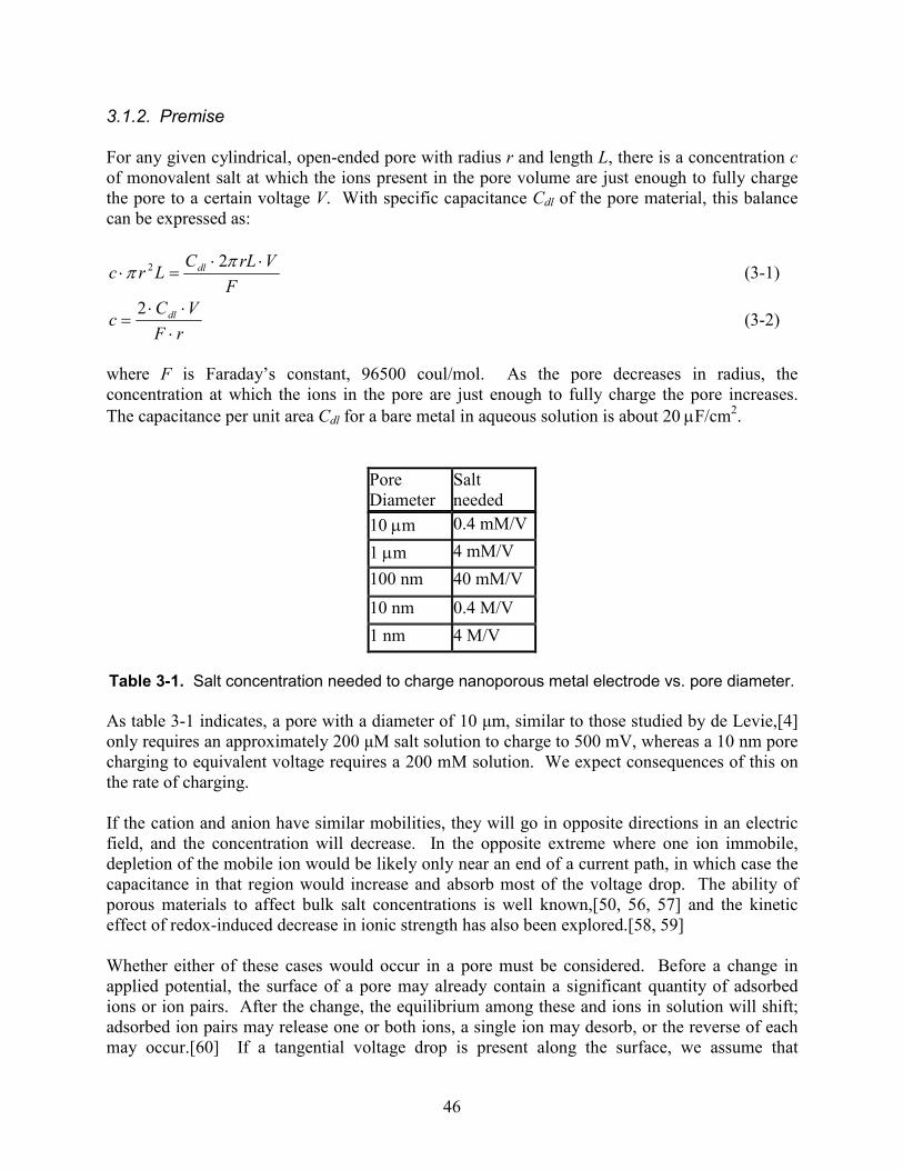
46
3.1.2. Premise For any given cylindrical, open-ended pore with radius r and length L, there is a concentration c of monovalent salt at which the ions present in the pore volume are just enough to fully charge the pore to a certain voltage V. With specific capacitance Cdl of the pore material, this balance can be expressed as:
F
VrLCLrc dl ⋅⋅=⋅
ππ
22 (3-1)
rF
VCc dl
⋅
⋅⋅=
2 (3-2)
where F is Faraday’s constant, 96500 coul/mol. As the pore decreases in radius, the concentration at which the ions in the pore are just enough to fully charge the pore increases. The capacitance per unit area Cdl for a bare metal in aqueous solution is about 20 µF/cm2.
Pore Diameter
Salt needed
10 µm 0.4 mM/V
1 µm 4 mM/V
100 nm 40 mM/V
10 nm 0.4 M/V
1 nm 4 M/V
Table 3-1. Salt concentration needed to charge nanoporous metal electrode vs. pore diameter.
As table 3-1 indicates, a pore with a diameter of 10 µm, similar to those studied by de Levie,[4] only requires an approximately 200 µM salt solution to charge to 500 mV, whereas a 10 nm pore charging to equivalent voltage requires a 200 mM solution. We expect consequences of this on the rate of charging. If the cation and anion have similar mobilities, they will go in opposite directions in an electric field, and the concentration will decrease. In the opposite extreme where one ion immobile, depletion of the mobile ion would be likely only near an end of a current path, in which case the capacitance in that region would increase and absorb most of the voltage drop. The ability of porous materials to affect bulk salt concentrations is well known,[50, 56, 57] and the kinetic effect of redox-induced decrease in ionic strength has also been explored.[58, 59] Whether either of these cases would occur in a pore must be considered. Before a change in applied potential, the surface of a pore may already contain a significant quantity of adsorbed ions or ion pairs. After the change, the equilibrium among these and ions in solution will shift; adsorbed ion pairs may release one or both ions, a single ion may desorb, or the reverse of each may occur.[60] If a tangential voltage drop is present along the surface, we assume that
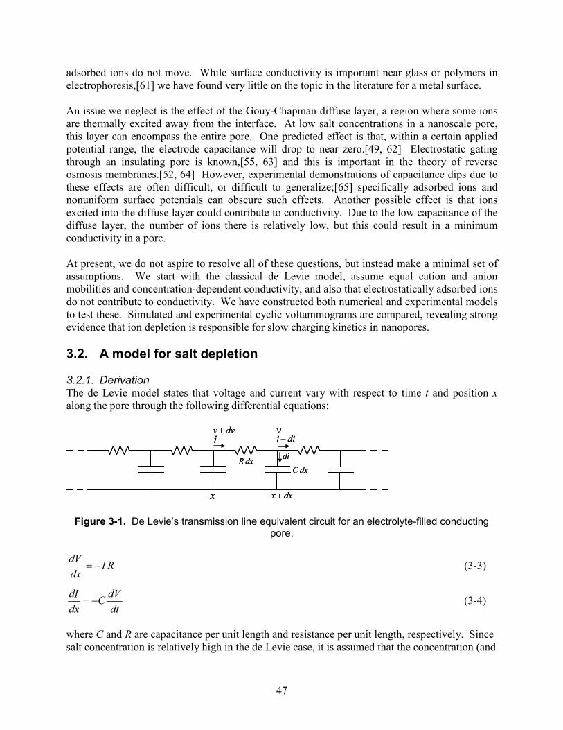
47
adsorbed ions do not move. While surface conductivity is important near glass or polymers in electrophoresis,[61] we have found very little on the topic in the literature for a metal surface. An issue we neglect is the effect of the Gouy-Chapman diffuse layer, a region where some ions are thermally excited away from the interface. At low salt concentrations in a nanoscale pore, this layer can encompass the entire pore. One predicted effect is that, within a certain applied potential range, the electrode capacitance will drop to near zero.[49, 62] Electrostatic gating through an insulating pore is known,[55, 63] and this is important in the theory of reverse osmosis membranes.[52, 64] However, experimental demonstrations of capacitance dips due to these effects are often difficult, or difficult to generalize;[65] specifically adsorbed ions and nonuniform surface potentials can obscure such effects. Another possible effect is that ions excited into the diffuse layer could contribute to conductivity. Due to the low capacitance of the diffuse layer, the number of ions there is relatively low, but this could result in a minimum conductivity in a pore. At present, we do not aspire to resolve all of these questions, but instead make a minimal set of assumptions. We start with the classical de Levie model, assume equal cation and anion mobilities and concentration-dependent conductivity, and also that electrostatically adsorbed ions do not contribute to conductivity. We have constructed both numerical and experimental models to test these. Simulated and experimental cyclic voltammograms are compared, revealing strong evidence that ion depletion is responsible for slow charging kinetics in nanopores.
3.2. A model for salt depletion 3.2.1. Derivation The de Levie model states that voltage and current vary with respect to time t and position x along the pore through the following differential equations:
x dxx +
dxCdxR
i dii −vdvv +
di
x dxx +
dxCdxR
i dii −vdvv +
di
Figure 3-1. De Levie’s transmission line equivalent circuit for an electrolyte-filled conducting
pore.
RIdx
dV−= (3-3)
dt
dVC
dx
dI−= (3-4)
where C and R are capacitance per unit length and resistance per unit length, respectively. Since salt concentration is relatively high in the de Levie case, it is assumed that the concentration (and
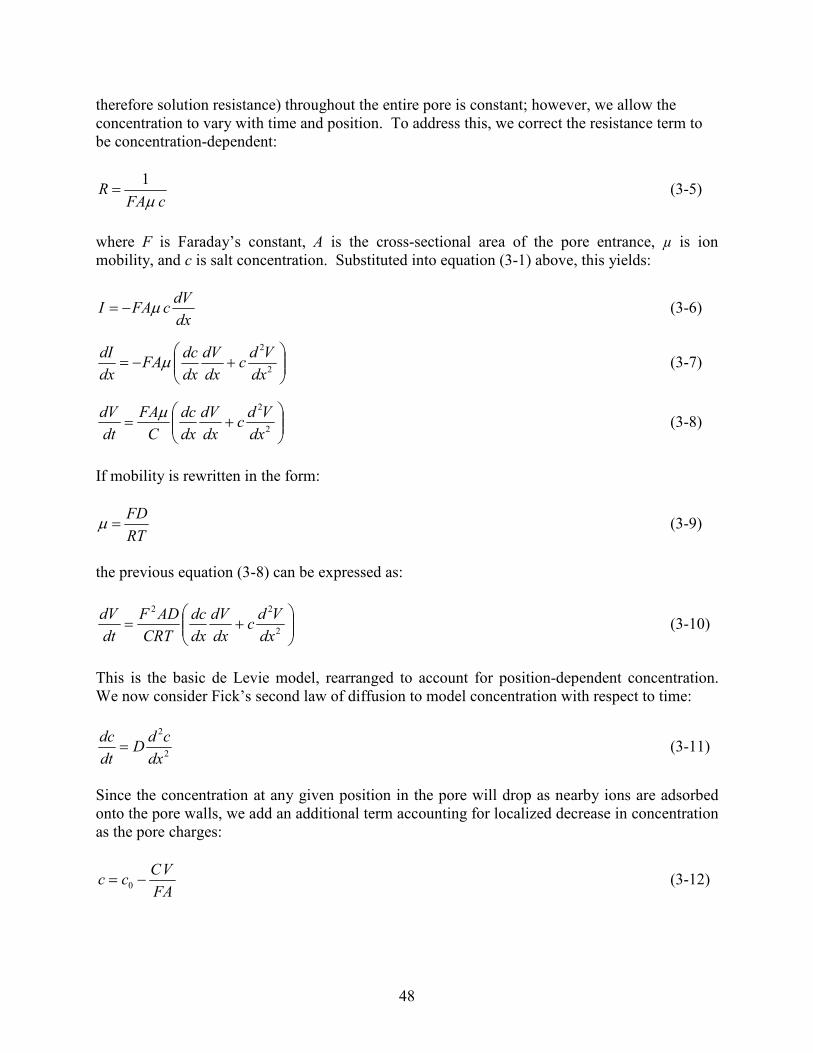
48
therefore solution resistance) throughout the entire pore is constant; however, we allow the concentration to vary with time and position. To address this, we correct the resistance term to be concentration-dependent:
cFAR
µ1
= (3-5)
where F is Faraday’s constant, A is the cross-sectional area of the pore entrance, µ is ion mobility, and c is salt concentration. Substituted into equation (3-1) above, this yields:
dx
dVcFAI µ−= (3-6)
+−=
2
2
dx
Vdc
dx
dV
dx
dcFA
dx
dIµ (3-7)
+=
2
2
dx
Vdc
dx
dV
dx
dc
C
FA
dt
dV µ (3-8)
If mobility is rewritten in the form:
RT
FD=µ (3-9)
the previous equation (3-8) can be expressed as:
+=
2
22
dx
Vdc
dx
dV
dx
dc
CRT
ADF
dt
dV (3-10)
This is the basic de Levie model, rearranged to account for position-dependent concentration. We now consider Fick’s second law of diffusion to model concentration with respect to time:
2
2
dx
cdD
dt
dc= (3-11)
Since the concentration at any given position in the pore will drop as nearby ions are adsorbed onto the pore walls, we add an additional term accounting for localized decrease in concentration as the pore charges:
FA
VCcc −= 0 (3-12)
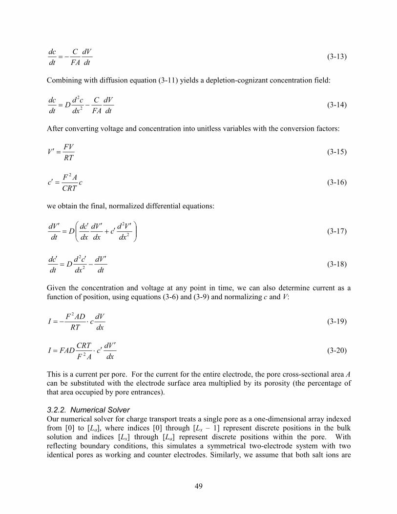
49
dt
dV
FA
C
dt
dc−= (3-13)
Combining with diffusion equation (3-11) yields a depletion-cognizant concentration field:
dt
dV
FA
C
dx
cdD
dt
dc−=
2
2
(3-14)
After converting voltage and concentration into unitless variables with the conversion factors:
RT
FVV =′ (3-15)
cCRT
AFc
2
=′ (3-16)
we obtain the final, normalized differential equations:
′′+
′′=′
2
2
dx
Vdc
dx
Vd
dx
cdD
dt
Vd (3-17)
dt
Vd
dx
cdD
dt
cd ′−′
=′
2
2
(3-18)
Given the concentration and voltage at any point in time, we can also determine current as a function of position, using equations (3-6) and (3-9) and normalizing c and V:
dx
dVc
RT
ADFI ⋅−=
2
(3-19)
dx
Vdc
AF
CRTFADI
′′⋅=
2 (3-20)
This is a current per pore. For the current for the entire electrode, the pore cross-sectional area A can be substituted with the electrode surface area multiplied by its porosity (the percentage of that area occupied by pore entrances). 3.2.2. Numerical Solver Our numerical solver for charge transport treats a single pore as a one-dimensional array indexed from [0] to [La], where indices [0] through [Lx – 1] represent discrete positions in the bulk solution and indices [Lx] through [La] represent discrete positions within the pore. With reflecting boundary conditions, this simulates a symmetrical two-electrode system with two identical pores as working and counter electrodes. Similarly, we assume that both salt ions are
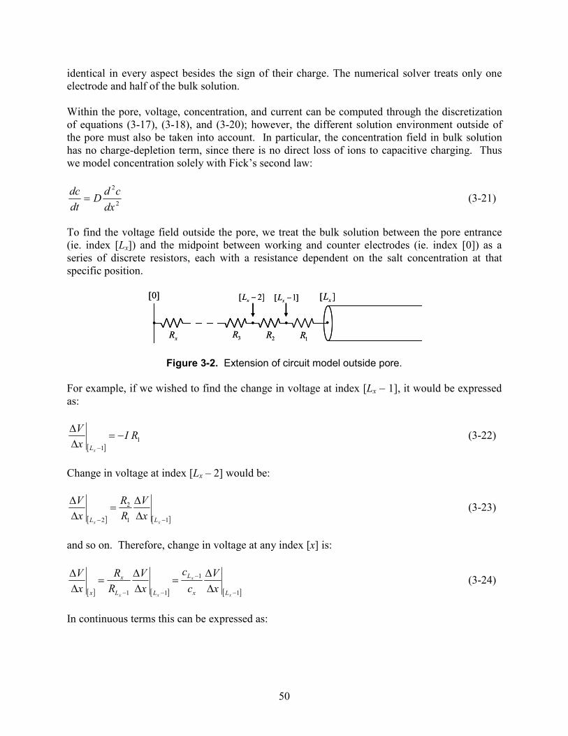
50
identical in every aspect besides the sign of their charge. The numerical solver treats only one electrode and half of the bulk solution. Within the pore, voltage, concentration, and current can be computed through the discretization of equations (3-17), (3-18), and (3-20); however, the different solution environment outside of the pore must also be taken into account. In particular, the concentration field in bulk solution has no charge-depletion term, since there is no direct loss of ions to capacitive charging. Thus we model concentration solely with Fick’s second law:
2
2
dx
cdD
dt
dc= (3-21)
To find the voltage field outside the pore, we treat the bulk solution between the pore entrance (ie. index [Lx]) and the midpoint between working and counter electrodes (ie. index [0]) as a series of discrete resistors, each with a resistance dependent on the salt concentration at that specific position.
]0[ ][ xL
1R2R3RxR
]1[ −xL]2[ −xL]0[ ][ xL
1R2R3RxR
]1[ −xL]2[ −xL
Figure 3-2. Extension of circuit model outside pore.
For example, if we wished to find the change in voltage at index [Lx – 1], it would be expressed as:
[ ]1
1
RIx
V
xL
−=∆∆
−
(3-22)
Change in voltage at index [Lx – 2] would be:
[ ] [ ]11
2
2 −− ∆∆
=∆∆
xx LL x
V
R
R
x
V (3-23)
and so on. Therefore, change in voltage at any index [x] is:
[ ] [ ] [ ]1
1
11 −
−
−− ∆∆
=∆∆
=∆∆
x
x
xx Lx
L
LL
x
x x
V
c
c
x
V
R
R
x
V (3-24)
In continuous terms this can be expressed as:
51
0
0
x
x
dx
Vd
c
c
dx
Vd ′′
′=′
(3-25)
where x0 is the pore entrance. We define the voltage at index [Lx] as the numerical solver’s computational input; however, for the purpose of simulating of a cyclic voltammogram, we desire the voltage at index [0] to be the input, since it represents exactly one half the voltage difference between the working and counter electrodes, which is what our instruments control. To indirectly “define” the voltage at index [0], we employ proportional control in the numerical solver. Thus in the simulation’s output, current is measured with regards to the voltage at index [0], rather than at index [Lx]. The C++ implementation of this is presented in the Appendix.
3.3. Simulation results and discussion Our cyclic voltammetry simulations ran between 0 and 10 thermal voltages (0 to 250 mV), at various starting concentrations and voltage ramp rates. In addition, we also tuned the value of Lx, the portion of the array representing the bulk solution, to simulate external solution resistance. We use simulation parameters comparable to our experiments, which use 100 µm radius, 2 cm long dealloyed gold wire electrodes with 10 nm pores with a 20 µm separator membrane. We assume Cdl = 20 µF/cm2, porosity is 0.5, and the diffusion constant is 10-5 cm2/s. When fully charged, these wires are expected to consume about 100 mM salt from the volume of their pores. The model assumes the electrode starts and ends the voltammogram with no adsorbed ions, but in reality this is almost certainly not the case. In practice, this would dampen the effect of depletion in real electrodes, since at any given point in a voltammogram both positive and negative charges are being adsorbed and released from the electrode, and the pore interior is never entirely vacated of ions. Regardless, in the ideal case, 0 mV represents the potential of zero adsorbed charge. When the voltammogram scans into positive voltage, anions adsorb onto the electrode surface, while cations are electrostatically driven out of the pore (the opposite occurs at the counter electrode, where cations are adsorbed and anions are driven into the bulk solution). In a situation of low concentration and equal ion mobility, our theory predicts ions will deplete from the liquid volume of the pore. When bias reaches 250 mV and the voltammogram scans back towards 0 mV, anions are discharged from the surface while cations are pulled back into the pore. The scan stops at 0 mV, and if at equilibrium, the electrode once again has no adsorbed ions. If the ramp rate is slow enough, the electrode charges like a normal capacitor in both scan directions, since the time scale is long enough such that charging is not diffusion-limited. In this case, the voltammogram is box-shaped.
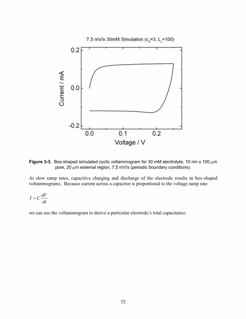
52
Figure 3-3. Box-shaped simulated cyclic voltammogram for 30 mM electrolyte, 10 nm x 100 µm
pore, 20 µm external region, 7.5 mV/s (periodic boundary conditions).
At slow ramp rates, capacitive charging and discharge of the electrode results in box-shaped voltammograms. Because current across a capacitor is proportional to the voltage ramp rate:
dt
dVCI =
we can use the voltammogram to derive a particular electrode’s total capacitance.
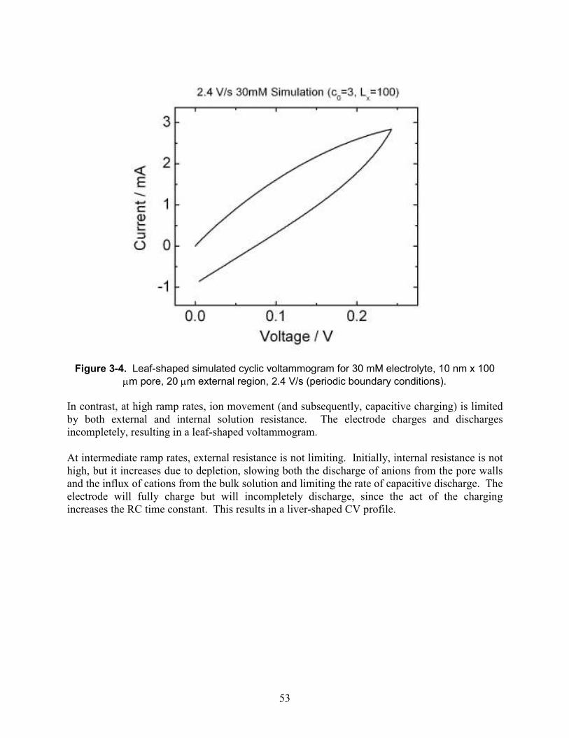
53
Figure 3-4. Leaf-shaped simulated cyclic voltammogram for 30 mM electrolyte, 10 nm x 100
µm pore, 20 µm external region, 2.4 V/s (periodic boundary conditions).
In contrast, at high ramp rates, ion movement (and subsequently, capacitive charging) is limited by both external and internal solution resistance. The electrode charges and discharges incompletely, resulting in a leaf-shaped voltammogram. At intermediate ramp rates, external resistance is not limiting. Initially, internal resistance is not high, but it increases due to depletion, slowing both the discharge of anions from the pore walls and the influx of cations from the bulk solution and limiting the rate of capacitive discharge. The electrode will fully charge but will incompletely discharge, since the act of the charging increases the RC time constant. This results in a liver-shaped CV profile.
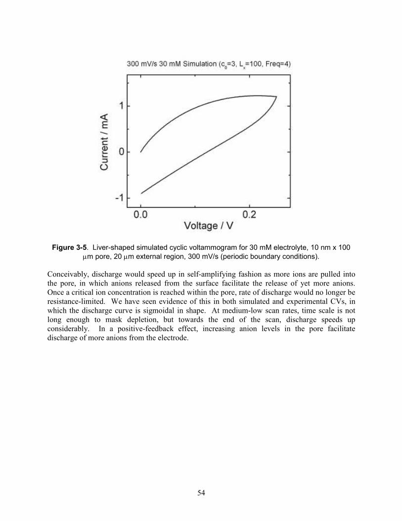
54
Figure 3-5. Liver-shaped simulated cyclic voltammogram for 30 mM electrolyte, 10 nm x 100
µm pore, 20 µm external region, 300 mV/s (periodic boundary conditions).
Conceivably, discharge would speed up in self-amplifying fashion as more ions are pulled into the pore, in which anions released from the surface facilitate the release of yet more anions. Once a critical ion concentration is reached within the pore, rate of discharge would no longer be resistance-limited. We have seen evidence of this in both simulated and experimental CVs, in which the discharge curve is sigmoidal in shape. At medium-low scan rates, time scale is not long enough to mask depletion, but towards the end of the scan, discharge speeds up considerably. In a positive-feedback effect, increasing anion levels in the pore facilitate discharge of more anions from the electrode.
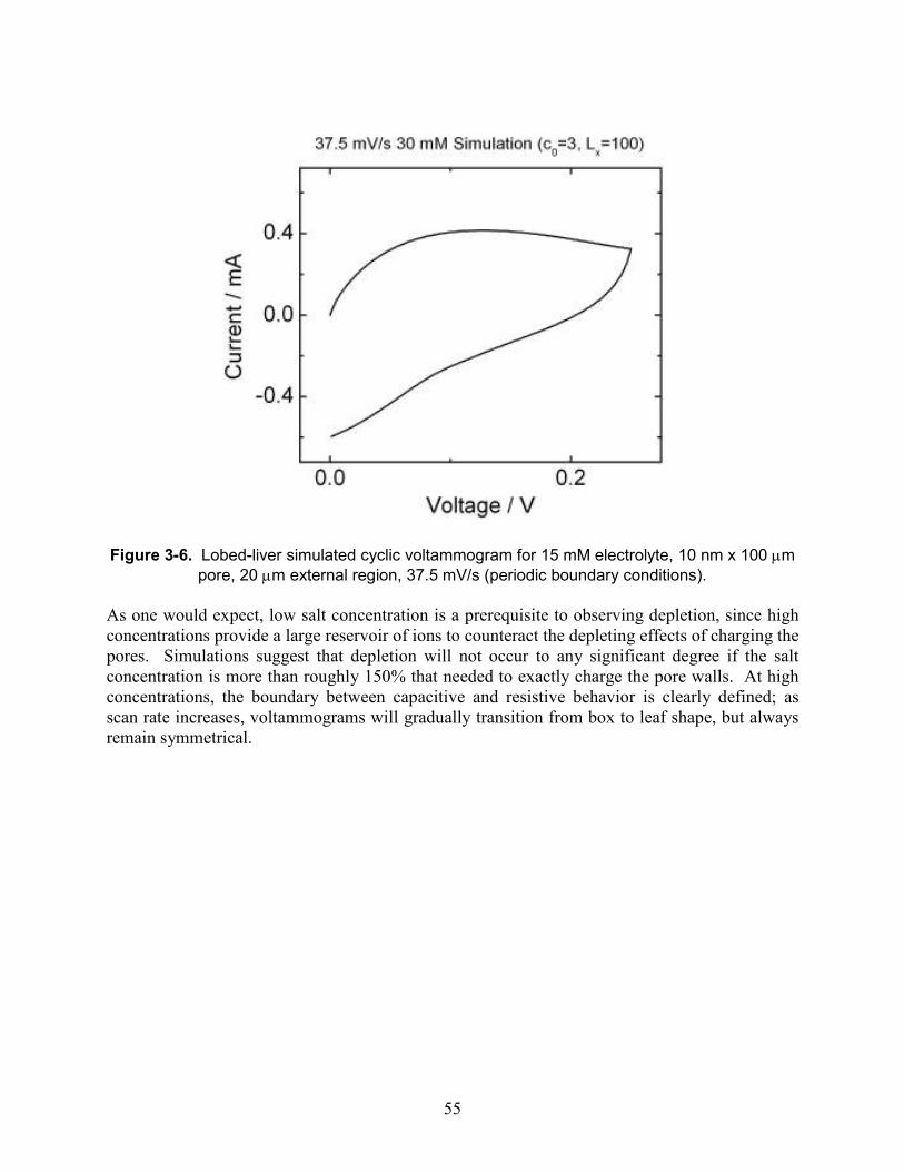
55
Figure 3-6. Lobed-liver simulated cyclic voltammogram for 15 mM electrolyte, 10 nm x 100 µm
pore, 20 µm external region, 37.5 mV/s (periodic boundary conditions).
As one would expect, low salt concentration is a prerequisite to observing depletion, since high concentrations provide a large reservoir of ions to counteract the depleting effects of charging the pores. Simulations suggest that depletion will not occur to any significant degree if the salt concentration is more than roughly 150% that needed to exactly charge the pore walls. At high concentrations, the boundary between capacitive and resistive behavior is clearly defined; as scan rate increases, voltammograms will gradually transition from box to leaf shape, but always remain symmetrical.
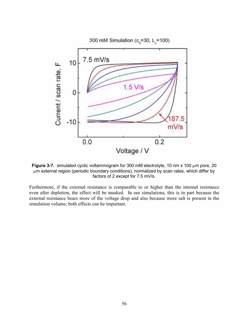
56
Figure 3-7. simulated cyclic voltammogram for 300 mM electrolyte, 10 nm x 100 µm pore, 20
µm external region (periodic boundary conditions), normalized by scan rates, which differ by factors of 2 except for 7.5 mV/s.
Furthermore, if the external resistance is comparable to or higher than the internal resistance even after depletion, the effect will be masked. In our simulations, this is in part because the external resistance bears more of the voltage drop and also because more salt is present in the simulation volume; both effects can be important.
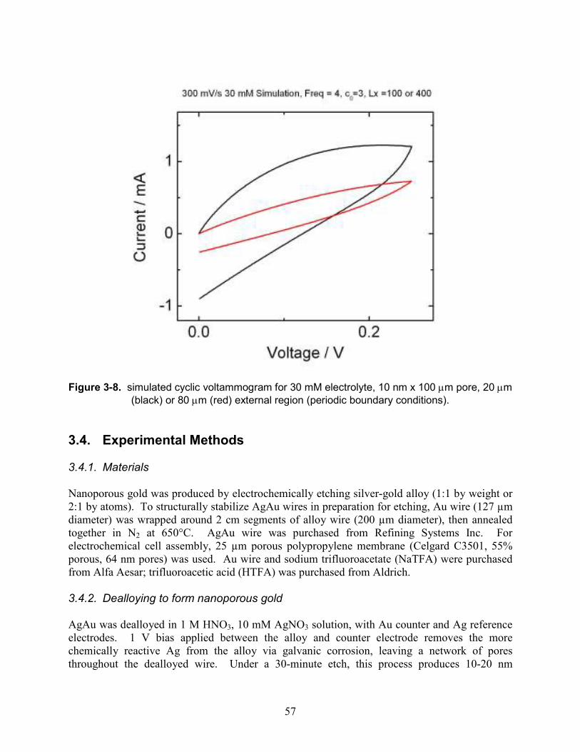
57
Figure 3-8. simulated cyclic voltammogram for 30 mM electrolyte, 10 nm x 100 µm pore, 20 µm
(black) or 80 µm (red) external region (periodic boundary conditions).
3.4. Experimental Methods 3.4.1. Materials Nanoporous gold was produced by electrochemically etching silver-gold alloy (1:1 by weight or 2:1 by atoms). To structurally stabilize AgAu wires in preparation for etching, Au wire (127 µm diameter) was wrapped around 2 cm segments of alloy wire (200 µm diameter), then annealed together in N2 at 650°C. AgAu wire was purchased from Refining Systems Inc. For electrochemical cell assembly, 25 µm porous polypropylene membrane (Celgard C3501, 55% porous, 64 nm pores) was used. Au wire and sodium trifluoroacetate (NaTFA) were purchased from Alfa Aesar; trifluoroacetic acid (HTFA) was purchased from Aldrich. 3.4.2. Dealloying to form nanoporous gold AgAu was dealloyed in 1 M HNO3, 10 mM AgNO3 solution, with Au counter and Ag reference electrodes. 1 V bias applied between the alloy and counter electrode removes the more chemically reactive Ag from the alloy via galvanic corrosion, leaving a network of pores throughout the dealloyed wire. Under a 30-minute etch, this process produces 10-20 nm
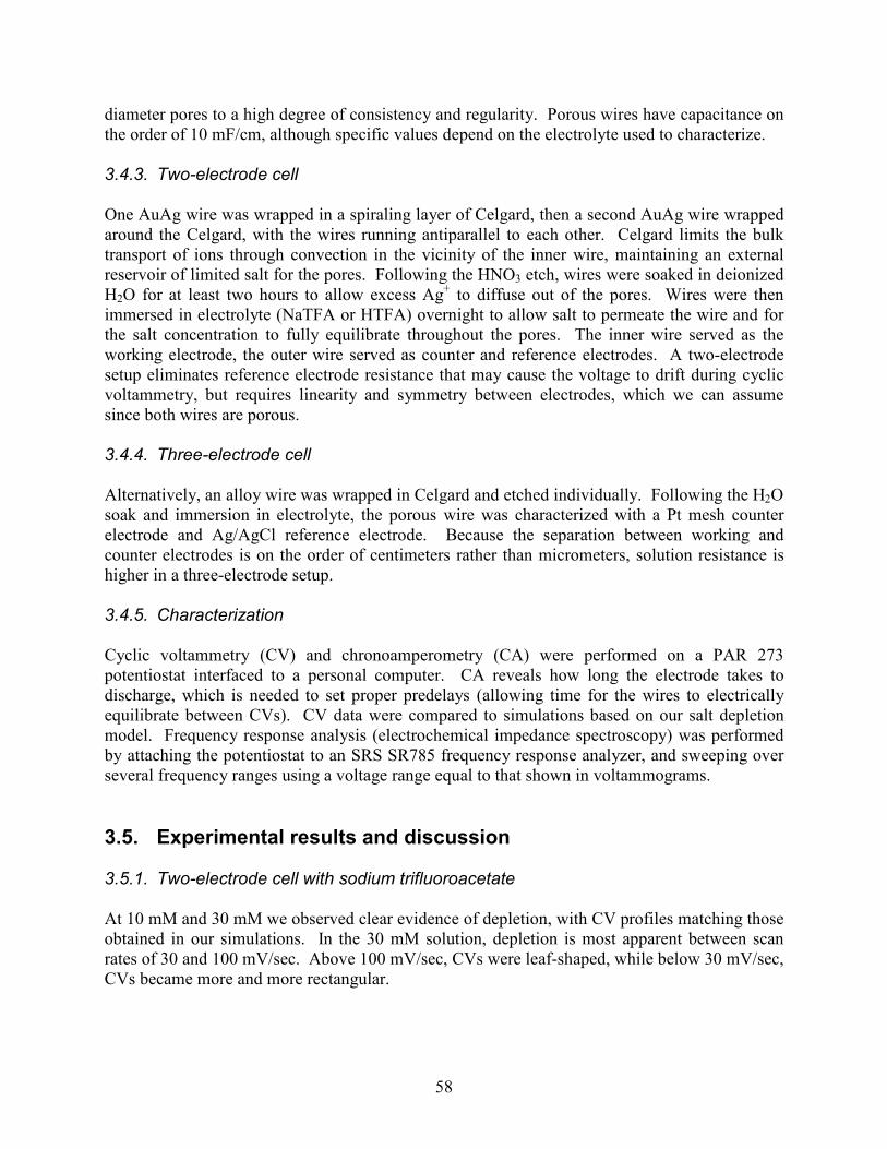
58
diameter pores to a high degree of consistency and regularity. Porous wires have capacitance on the order of 10 mF/cm, although specific values depend on the electrolyte used to characterize. 3.4.3. Two-electrode cell One AuAg wire was wrapped in a spiraling layer of Celgard, then a second AuAg wire wrapped around the Celgard, with the wires running antiparallel to each other. Celgard limits the bulk transport of ions through convection in the vicinity of the inner wire, maintaining an external reservoir of limited salt for the pores. Following the HNO3 etch, wires were soaked in deionized H2O for at least two hours to allow excess Ag+ to diffuse out of the pores. Wires were then immersed in electrolyte (NaTFA or HTFA) overnight to allow salt to permeate the wire and for the salt concentration to fully equilibrate throughout the pores. The inner wire served as the working electrode, the outer wire served as counter and reference electrodes. A two-electrode setup eliminates reference electrode resistance that may cause the voltage to drift during cyclic voltammetry, but requires linearity and symmetry between electrodes, which we can assume since both wires are porous. 3.4.4. Three-electrode cell Alternatively, an alloy wire was wrapped in Celgard and etched individually. Following the H2O soak and immersion in electrolyte, the porous wire was characterized with a Pt mesh counter electrode and Ag/AgCl reference electrode. Because the separation between working and counter electrodes is on the order of centimeters rather than micrometers, solution resistance is higher in a three-electrode setup. 3.4.5. Characterization Cyclic voltammetry (CV) and chronoamperometry (CA) were performed on a PAR 273 potentiostat interfaced to a personal computer. CA reveals how long the electrode takes to discharge, which is needed to set proper predelays (allowing time for the wires to electrically equilibrate between CVs). CV data were compared to simulations based on our salt depletion model. Frequency response analysis (electrochemical impedance spectroscopy) was performed by attaching the potentiostat to an SRS SR785 frequency response analyzer, and sweeping over several frequency ranges using a voltage range equal to that shown in voltammograms.
3.5. Experimental results and discussion 3.5.1. Two-electrode cell with sodium trifluoroacetate At 10 mM and 30 mM we observed clear evidence of depletion, with CV profiles matching those obtained in our simulations. In the 30 mM solution, depletion is most apparent between scan rates of 30 and 100 mV/sec. Above 100 mV/sec, CVs were leaf-shaped, while below 30 mV/sec, CVs became more and more rectangular.
59
In experiments, the observed effect was not dependent on starting point. Scanning at 60 mV/s from 400 to –400 mV produced an upside-down liver shape. This suggests that the two-electrode cell is behaving symmetrically; the wires do not charge differently when loaded with cations or anions, and the depletion effect does not depend on a potential of zero adsorbed salt, if one exists.
Figure 3-9. Experimental voltammograms for two-electrode porous gold wire cells in 30 mM
sodium trifluoroacetate at varying scan rates. The left and right plots show the same 10 and 60 mV/s scans on different scales.
In 10 mM NaTFA we observed a similar pattern, although in this case liver-shaped voltammograms were observed between 6 and 30 mV/sec. This reflects the increase in solution resistance produced by a reduction in salt concentration. The resulting RC time is longer than that of the 30 mM solution, leading to a generally longer time scale for pore charging and depletion.
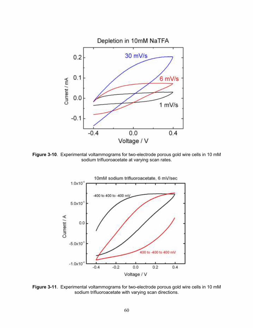
60
Figure 3-10. Experimental voltammograms for two-electrode porous gold wire cells in 10 mM
sodium trifluoroacetate at varying scan rates.
Figure 3-11. Experimental voltammograms for two-electrode porous gold wire cells in 10 mM
sodium trifluoroacetate with varying scan directions.
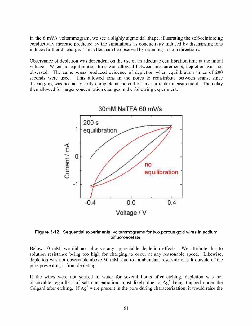
61
In the 6 mV/s voltammogram, we see a slighly sigmoidal shape, illustrating the self-reinforcing conductivity increase predicted by the simulations as conductivity induced by discharging ions induces further discharge. This effect can be observed by scanning in both directions. Observance of depletion was dependent on the use of an adequate equilibration time at the initial voltage. When no equilibration time was allowed between measurements, depletion was not observed. The same scans produced evidence of depletion when equilibration times of 200 seconds were used. This allowed ions in the pores to redistribute between scans, since discharging was not necessarily complete at the end of any particular measurement. The delay then allowed for larger concentration changes in the following experiment.
Figure 3-12. Sequential experimental voltammograms for two porous gold wires in sodium
trifluoroacetate.
Below 10 mM, we did not observe any appreciable depletion effects. We attribute this to solution resistance being too high for charging to occur at any reasonable speed. Likewise, depletion was not observable above 30 mM, due to an abundant reservoir of salt outside of the pore preventing it from depleting. If the wires were not soaked in water for several hours after etching, depletion was not observable regardless of salt concentration, most likely due to Ag+ being trapped under the Celgard after etching. If Ag+ were present in the pore during characterization, it would raise the
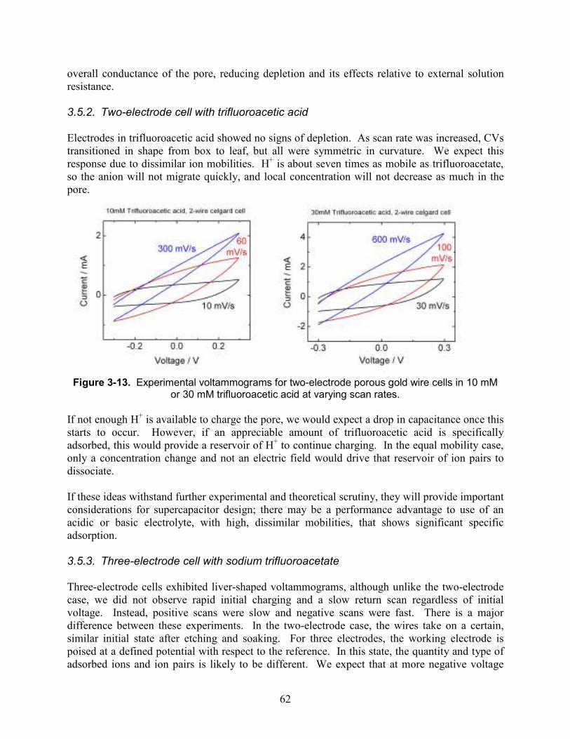
62
overall conductance of the pore, reducing depletion and its effects relative to external solution resistance. 3.5.2. Two-electrode cell with trifluoroacetic acid Electrodes in trifluoroacetic acid showed no signs of depletion. As scan rate was increased, CVs transitioned in shape from box to leaf, but all were symmetric in curvature. We expect this response due to dissimilar ion mobilities. H+ is about seven times as mobile as trifluoroacetate, so the anion will not migrate quickly, and local concentration will not decrease as much in the pore.
Figure 3-13. Experimental voltammograms for two-electrode porous gold wire cells in 10 mM
or 30 mM trifluoroacetic acid at varying scan rates.
If not enough H+ is available to charge the pore, we would expect a drop in capacitance once this starts to occur. However, if an appreciable amount of trifluoroacetic acid is specifically adsorbed, this would provide a reservoir of H+ to continue charging. In the equal mobility case, only a concentration change and not an electric field would drive that reservoir of ion pairs to dissociate. If these ideas withstand further experimental and theoretical scrutiny, they will provide important considerations for supercapacitor design; there may be a performance advantage to use of an acidic or basic electrolyte, with high, dissimilar mobilities, that shows significant specific adsorption. 3.5.3. Three-electrode cell with sodium trifluoroacetate Three-electrode cells exhibited liver-shaped voltammograms, although unlike the two-electrode case, we did not observe rapid initial charging and a slow return scan regardless of initial voltage. Instead, positive scans were slow and negative scans were fast. There is a major difference between these experiments. In the two-electrode case, the wires take on a certain, similar initial state after etching and soaking. For three electrodes, the working electrode is poised at a defined potential with respect to the reference. In this state, the quantity and type of adsorbed ions and ion pairs is likely to be different. We expect that at more negative voltage
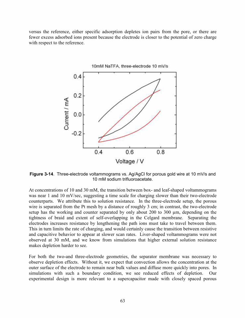
63
versus the reference, either specific adsorption depletes ion pairs from the pore, or there are fewer excess adsorbed ions present because the electrode is closer to the potential of zero charge with respect to the reference.
Figure 3-14. Three-electrode voltammograms vs. Ag/AgCl for porous gold wire at 10 mV/s and
10 mM sodium trifluoroacetate.
At concentrations of 10 and 30 mM, the transition between box- and leaf-shaped voltammograms was near 1 and 10 mV/sec, suggesting a time scale for charging slower than their two-electrode counterparts. We attribute this to solution resistance. In the three-electrode setup, the porous wire is separated from the Pt mesh by a distance of roughly 3 cm; in contrast, the two-electrode setup has the working and counter separated by only about 200 to 300 µm, depending on the tightness of braid and extent of self-overlapping in the Celgard membrane. Separating the electrodes increases resistance by lengthening the path ions must take to travel between them. This in turn limits the rate of charging, and would certainly cause the transition between resistive and capacitive behavior to appear at slower scan rates. Liver-shaped voltammograms were not observed at 30 mM, and we know from simulations that higher external solution resistance makes depletion harder to see. For both the two-and three-electrode geometries, the separator membrane was necessary to observe depletion effects. Without it, we expect that convection allows the concentration at the outer surface of the electrode to remain near bulk values and diffuse more quickly into pores. In simulations with such a boundary condition, we see reduced effects of depletion. Our experimental design is more relevant to a supercapacitor made with closely spaced porous
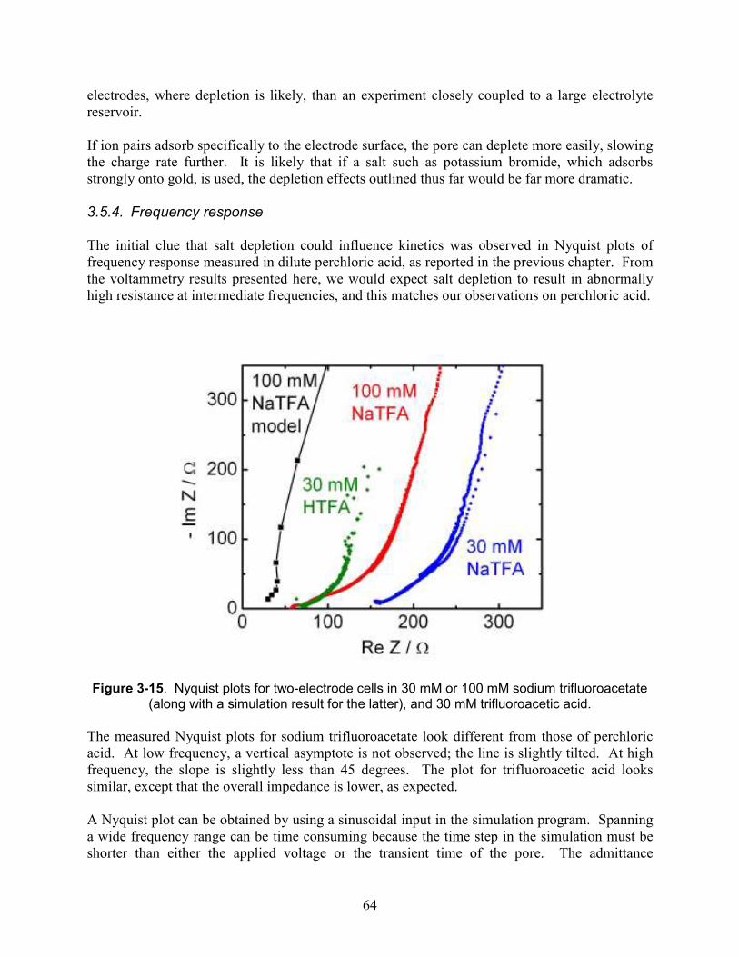
64
electrodes, where depletion is likely, than an experiment closely coupled to a large electrolyte reservoir. If ion pairs adsorb specifically to the electrode surface, the pore can deplete more easily, slowing the charge rate further. It is likely that if a salt such as potassium bromide, which adsorbs strongly onto gold, is used, the depletion effects outlined thus far would be far more dramatic. 3.5.4. Frequency response The initial clue that salt depletion could influence kinetics was observed in Nyquist plots of frequency response measured in dilute perchloric acid, as reported in the previous chapter. From the voltammetry results presented here, we would expect salt depletion to result in abnormally high resistance at intermediate frequencies, and this matches our observations on perchloric acid.
Figure 3-15. Nyquist plots for two-electrode cells in 30 mM or 100 mM sodium trifluoroacetate
(along with a simulation result for the latter), and 30 mM trifluoroacetic acid.
The measured Nyquist plots for sodium trifluoroacetate look different from those of perchloric acid. At low frequency, a vertical asymptote is not observed; the line is slightly tilted. At high frequency, the slope is slightly less than 45 degrees. The plot for trifluoroacetic acid looks similar, except that the overall impedance is lower, as expected. A Nyquist plot can be obtained by using a sinusoidal input in the simulation program. Spanning a wide frequency range can be time consuming because the time step in the simulation must be shorter than either the applied voltage or the transient time of the pore. The admittance
65
magnitude and phase was obtained by measuring current peak amplitudes and shifts with respect to the following voltage peak at steady state. The absolute current was matched to the observed capacitance at low frequency (about 10 mF). The simulated curve features a tilted asymptote, as well as the hypothesized shift to higher resistance during the transition to the low-slope region, along the same theme as our observations of dilute perchloric acid. Tilted asymptotes are frequently observed and attributed to various nonuniformities.[15] Nonuniform salt concentration could be expected to produce the same result. In general, though, we are hesitant to invest effort in the interpretation of these plots because salt depletion is a nonlinear effect; for this reason, we focused our investigation on voltammetry. However, the difference in Nyquist plots involving trifluoroacetate and perchlorate suggests that diverse mechanisms may be involved in depletion.
3.6. Conclusion We have provided qualitative and quantitative methods for describing the charging dynamics of nanoscale pores and have demonstrated that charging at low concentrations can deplete ions from the liquid volume of a pore. Because there are relatively few ions inside a nanopore compared to the number chemically or electrostatically bound to the interface, the act of charging the capacitor will increase its resistance, lengthening its time constant. This is not visible at slow scan rates, since there is enough time for the capacitor to fully charge and discharge, while at high scan rates, charging and discharging are already limited by solution resistance. At scan rates between those, the pore will charge fully, but due to increased local solution resistance from ion depletion, the discharge will be slower and incomplete. This phenomenon becomes more severe as pore size shrinks and has far-reaching practical implications. While gold pores deplete at concentrations in the millimolar range, a pore with less than 10 nm diameter, as would most likely be used in commercial energy storage applications, would deplete at over 1 M concentration – approaching or surpassing the saturation point of many salts. Our experimental data closely match our model’s predictions from a qualitative standpoint, with a transition range between capacitive and resistive frequencies in two-electrode systems that is well-defined in NaTFA setups but absent in HTFA. The asymmetrical voltammograms of three-electrode systems suggest that ion pair adsorption at high potentials that merits further investigation. The fact that experiments match our simple assumptions allows us to reconsider the physical phenomena that may be involved in this effect. We saw remarkably little change in capacitance as a function of concentration; we apparently do not require a detailed model for the Gouy-Chapman diffuse layer to explain our data. The fact that a depletion effect exists suggests that adsorbed salt does not play a major role in conduction. However, because a separator membrane was needed to observe increased resistance in voltammograms, we must consider the possibility that depletion occurs only in the gap between the wire and the membrane, in which case conductance in the pore would remain high. We believe we can rule that out because depletion occurs mainly on the timescale when
66
internal solution resistance is influencing the charging rate, and we observed related effects in perchloric acid with no membrane. Our observations answer the question of whether and under what conditions a depletion effect can occur. This information will be of value in the design of energy storage devices operating near their optimal design point, where external solution resistance is kept low. With attention to depletion phenomena, a designer can ensure that performance is not limited by those effects instead. Answering this question has opened up many others about the mechanism, especially the role of specific adsorption in enhancing or reducing depletion, and how the mechanism changes as mobilities go from symmetric to highly asymmetric. A greater understanding of this may provide further benefits to energy storage system design.
67
4. ELECTRICALLY TRIGGERED DRUG DELIVERY USING NANOPOROUS ELECTRODES
This work was an NSF-sponsored collaboration with Prof. Roger Narayan at the joint
bioengineering program of North Carolina State University and the University of North
Carolina. Bonnie Pierson visited Sandia in the summer of 2008 to optimize electrode design,
and Shaun Gittard visited in the summer of 2009 to study electrode performance. Max Wu and
Cindy Ha also contributed to this work.
4.0. Abstract Nanoporous electrodes, such as those made from carbon or gold, can capture and release ionic analytes at concentrations near 1 mole per liter of pore volume through capacitive charging or electrochemically reversible adsorption. In vitro studies suggest that this phenomenon can be the basis for a noninvasive, precise, and programmable drug delivery method. It eliminates the need for bulk fluid delivery to target tissue and requires only a thin electrical connection, minimizing pain and tissue disruption. Timing of release is controllable by adjusting voltage. Compared to injection, this process causes less pain and tissue damage and more local delivery. Compared to iontophoretic methods, there is minimal involvement of ions other than the drug, and applied voltages can be lower, further reducing tissue disruption. We have designed effective gold electrode assemblies and achieved voltage-controlled charge and release of model pharmaceuticals (salicylate) using electrochemical methods.
4.1. Introduction 4.1.1. Background Orally administered drugs are generally preferred by patients and medical staff due to their ease of administration. However numerous pharmaceuticals, particularly protein and nucleic acid based drugs, are rapidly metabolized by the stomach and liver rendering them impractical for the oral route.[66] Therefore, direct administration of pharmaceuticals into the bloodstream is still a necessity. Injection is the most widely used technique to deliver pharmaceuticals directly into the bloodstream or specific tissue. Nevertheless injection has numerous undesirable properties. Sharp needles pose an injury risk to both patients and medical personnel. While sharps injury rates in the United States are relatively low (0.18 injuries per healthcare worker per year), injury rates in less developed countries can be exceptionally high (up to 4.7 injuries per healthcare worker per year).[67] Also, pain is commonly associated with injections. A study by Bartell et al. found that average VAS pain scores for hypodermic needle subcutaneous insertion was 39 mm on a 100 mm scale. 35% of patients reported persistence of mild to moderate pain at 3 days after receiving an injected vaccination.[68] The pain from injections can be particularly distressing for children. Studies have reported that 8.6% of young adults have a fear of injections.[69] 20% of children are severely distressed by vaccinations.[70] In addition to the obvious goal of improving patient comfort, minimizing pain will also help patient compliance. For example, 8% of patients
68
choosing to not receive seasonal influenza immunizations due to the pain associated with the procedure.[68] While needles themselves can cause pain, much of the discomfort from injections is due to the drug itself. Drugs must be administered in liquid form in order to be compatible with injection. Injecting fluid into tissue causes swelling, tissue damage, and resultant pain.[71] Accordingly, larger injection volumes result in greater pain.[72] In some cases the pain and tissue damage from injections is caused by solvents or drugs that are irritants, especially lipid soluble molecules.[73-75] This fluid driven tissue damage is why pain from an injection is often felt over a relatively large area for well after the injection has occurred. In some cases, tissue damage from injections can cause bruising.[76] Several alternatives to injection have been developed for directly administering pharmaceuticals into the bloodstream. With 19 systems on the market and more under clinical trials, transdermal patches are the most widely used injection alternative for direct delivery to the bloodstream.[77] The use of transdermal patches, however, is rather limited. The stratum corneum, the outermost layer of the skin, is a potent diffusion barrier. This 10-40 mm thick layer of lipids and dead cells is particularly effective at preventing diffusion of large, charged, or polar molecules.[78-80] Consequently, transdermal patches have been limited to small molecular weight neutral pharmaceuticals. A number of new technologies have been developed to improve the diffusivity of the skin, enabling a greater number of drugs to be compatible with transdermal patches. One technique to improve the diffusion coefficient of the stratum corneum is to disrupting the ordered lipid structure. Chemical penetration enhancers alter the bonding lipids which disorganizes the structure, thus improving permeability.[81] Unfortunately chemical penetration enhancers are often associated with skin irritation.[77] As with penetration enhancers, ultrasound has been shown to improve the diffusivity of the stratum corneum by disrupting lipid structure.[82] Ultrasound at low frequencies (~20 kHz) induces the formation of cavitation bubbles that reversibly increase the permeability of the stratum corneum.[83] Cavitational ultrasound is only effective for improving diffusivity of small molecules, which limits its pharmaceutical applications.[77] Electroporation, millisecond high-voltage pulses of electricity, also disorganizes the lipid bilayer and improves permeability.[84] This technique has been shown to improve diffusion of a number of macromolecules including vaccines, DNA, and peptides.[77] Delivery of molecules up to 7 kDa via electroporation have been reported.[85] Instead of disturbing the lipid bilayer, microneedles physically create tiny holes in the stratum corneum. Drugs can then be delivered via this direct pathway through the stratum corneum. Since a direct micron-sized pathway is created, molecule size and charge are not limiting factors. These needles are of a size where they pierce the stratum corneum but do not reach nerve cells located in the deeper skin layers. Therefore there is no pain associated with piercing the skin.[86] Drug delivery via microneedles has been performed in a number of ways, including coating the needles,[87] suspension in a dissolving microneedle,[88-90] and injection.[91-93] One disadvantage of diffusion controlled release is that it is difficult to control the dose rate, whereas injection allows real time dose control. However, injection via microneedles has the same fluid problems that are associated with traditional needles.
69
In iontophoresis, a low voltage current is used to drive molecules across the stratum corneum. An electrical current carries charged molecules from one reservoir toward the other. Along this path, they pass through the stratum corneum and enter the bloodstream.[94] This method is most efficient with delivering charged molecules, though transport of neutral molecules has also been achieved.[95] The benefit of this technique is that dose rate can be easily controlled by the voltage applied between the reservoirs. On the other hand, there are several drawbacks with iontophoresis. Regulations require currents to remain below 0.5 mA cm-2 which limits delivery rates.[66] The current can also cause irritation and damage to the skin. Lastly ions in tissue and counter ions in the device such as Na+ and Cl- with high mobilities can balance the voltage difference which limits the degree of drug transfer.[94] 4.1.2. Capacitive delivery We propose electrically induced delivery from a porous electrode as a method for direct administration of pharmaceutical agents to the bloodstream. In this technique, electrochemical double-layer supercapacitors are used to administer charged pharmaceutical agents. A double layer capacitor consists of two electrodes in a salt solution. When a voltage is applied between the two electrodes, an increased number of anions in the salt solution are electrostatically adsorbed onto the surface of the positively biased electrode (working electrode). Likewise, cations in the solution are adsorbed onto the opposite electrode (counter electrode). In an ideal capacitor, the applied voltage is proportional to the amount of charge adsorbed to the surface. Thus, when one reduces the voltage between the electrodes adsorbed ions are released from the surface. In the case of capacitive drug delivery, the anion or cation is a charged pharmacologic molecule. An ordinary parallel-plate electrode pair does not have the storage capacity to deliver medically relevant concentrations of drugs. For example the specific capacitance of a planar bare metal electrode Cdl charged with a typical salt such as sodium chloride is approximately 10-5 F/cm2. Converted with Faraday’s constant F = 105 coulombs/mole, this is 10-10 moles/V cm2. Charged to 1 volt, an electrode pair the size of a football field would be required to store just a few millimoles of a charged drug. However, such areas can be incorporated into small volumes using nano-porous electrodes, where each point in the electrode is within a few atoms of a surface. These electrodes can be modeled as arrays of cylindrical pores, each with a capacitance of
rLCC dlpore π2=
If the electrode is a cube, and the pores are densely packed in a square array, separated by one pore radius (35% pore volume), the number of pores is L2/(3r)2. The capacitance per unit volume is then
r
CC dl
vol9
2π=
and the molarity of stored salt in the electrode per volt is
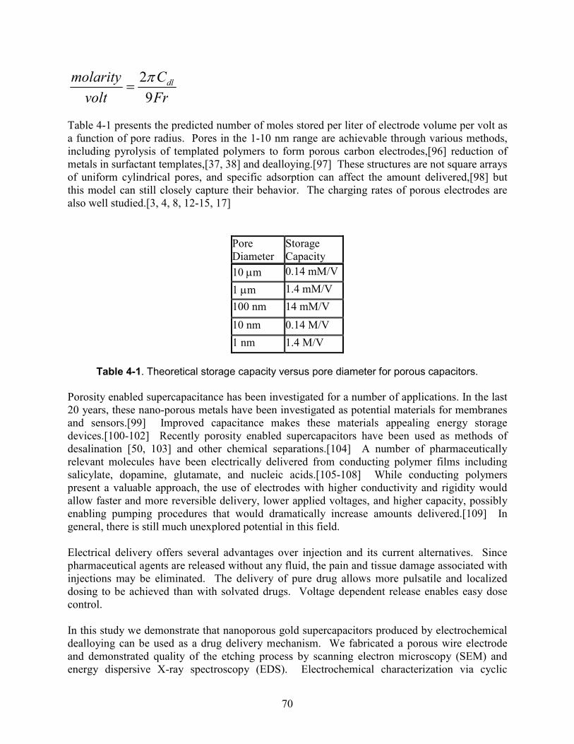
70
Fr
C
volt
molarity dl
9
2π=
Table 4-1 presents the predicted number of moles stored per liter of electrode volume per volt as a function of pore radius. Pores in the 1-10 nm range are achievable through various methods, including pyrolysis of templated polymers to form porous carbon electrodes,[96] reduction of metals in surfactant templates,[37, 38] and dealloying.[97] These structures are not square arrays of uniform cylindrical pores, and specific adsorption can affect the amount delivered,[98] but this model can still closely capture their behavior. The charging rates of porous electrodes are also well studied.[3, 4, 8, 12-15, 17]
Pore Diameter
Storage Capacity
10 µm 0.14 mM/V
1 µm 1.4 mM/V
100 nm 14 mM/V
10 nm 0.14 M/V
1 nm 1.4 M/V
Table 4-1. Theoretical storage capacity versus pore diameter for porous capacitors.
Porosity enabled supercapacitance has been investigated for a number of applications. In the last 20 years, these nano-porous metals have been investigated as potential materials for membranes and sensors.[99] Improved capacitance makes these materials appealing energy storage devices.[100-102] Recently porosity enabled supercapacitors have been used as methods of desalination [50, 103] and other chemical separations.[104] A number of pharmaceutically relevant molecules have been electrically delivered from conducting polymer films including salicylate, dopamine, glutamate, and nucleic acids.[105-108] While conducting polymers present a valuable approach, the use of electrodes with higher conductivity and rigidity would allow faster and more reversible delivery, lower applied voltages, and higher capacity, possibly enabling pumping procedures that would dramatically increase amounts delivered.[109] In general, there is still much unexplored potential in this field. Electrical delivery offers several advantages over injection and its current alternatives. Since pharmaceutical agents are released without any fluid, the pain and tissue damage associated with injections may be eliminated. The delivery of pure drug allows more pulsatile and localized dosing to be achieved than with solvated drugs. Voltage dependent release enables easy dose control. In this study we demonstrate that nanoporous gold supercapacitors produced by electrochemical dealloying can be used as a drug delivery mechanism. We fabricated a porous wire electrode and demonstrated quality of the etching process by scanning electron microscopy (SEM) and energy dispersive X-ray spectroscopy (EDS). Electrochemical characterization via cyclic
71
voltammetry and chronoamperometry confirmed the proper capacitive behavior of the nanoporous gold electrodes using both simple salts and a model drug, benzylammonium salicylate. Loading and delivery of the model drug was demonstrated through both electrical and spectroscopic monitoring.
4.2. Experimental Methods 4.2.1. Dealloying to form nanoporous gold All chemicals were supplied by Sigma-Aldrich (Sigma-Aldrich, St. Louis, MO). Electrochemical etching of 1:1 weight ratio Au-Ag alloy wires (Refining Systems Inc, Las Vegas, NV) was performed to create nanoporous Au wires. First a 0.1 mm diameter gold wire (Alfa Aesar, Ward Hill, MA) was loosely coiled around a 2 cm segment of the 0.2 mm diameter Au-Ag alloy wire. Coiling density was approximately 5 turns per cm. The nano-porous wires are brittle; the pure gold wire provided for easier handling after etching, and also ensured that a defined porous wire length was exposed to the solution.[97] The braided wires were then annealed under nitrogen at 650 C overnight, which helps prevent cracking of the nano-porous structure. The annealed wires were then placed in a bath of 1M HNO3 and 10 mM AgNO3. The annealed alloy wires, a platinum wire, and a silver wire were then connected to the working, counter, and reference leads of a potentiostat (Model 273A, Princeton Applied Research, Oak Ridge, TN), respectively. A diagram of this etching setup is provided in Figure 4-1a. A voltage of 1200 mV was then applied for 30 minutes between the working and counter electrodes to initiate the dealloying process. The applied voltage induces galvanic corrosion of the alloy which resulted in transfer of silver to the counter electrode. The departure of silver results in the formation of nano-scale pores in the alloy. 4.2.2. Analysis of gold wire Field emission canning electron microscopy (JEOL 6400F, Tokyo, Japan) was performed on electrochemically etched gold wires to determine their surface morphology. Spectroscopy via energy dispersive X-ray spectroscopy (EDS) was carried out to determine the elemental composition of the etched wires (Hitachi S-3200, Hitachi Ltd, Tokyo, Japan). 4.2.3. Cell setup Two holes were punctured in the lid of a 4 mL cuvette, and an unetched wire was threaded through each hole to allow the wires to be handled simultaneously without coming in contact during the experiments. The wires were then submerged into etching solution and dealloyed. Following that, wires were soaked in deionized H2O for at least two hours to allow excess Ag+ to diffuse out of the pores. The lid was then capped onto a cuvette of analyte (sodium trifluoroacetate (NaTFA), benzylammonium salicylate (BzAmSal), and MgSO4 were used in our trials), with one wire as working electrode and the other as counter and reference.
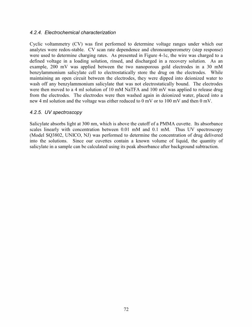
72
4.2.4. Electrochemical characterization Cyclic voltammetry (CV) was first performed to determine voltage ranges under which our analytes were redox-stable. CV scan rate dependence and chronoamperometry (step response) were used to determine charging rates. As presented in Figure 4-1c, the wire was charged to a defined voltage in a loading solution, rinsed, and discharged in a recovery solution. As an example, 200 mV was applied between the two nanoporous gold electrodes in a 30 mM benzylammonium salicylate cell to electrostatically store the drug on the electrodes. While maintaining an open circuit between the electrodes, they were dipped into deionized water to wash off any benzylammonium salicylate that was not electrostatically bound. The electrodes were then moved to a 4 ml solution of 10 mM NaTFA and 100 mV was applied to release drug from the electrodes. The electrodes were then washed again in deionized water, placed into a new 4 ml solution and the voltage was either reduced to 0 mV or to 100 mV and then 0 mV. 4.2.5. UV spectroscopy Salicylate absorbs light at 300 nm, which is above the cutoff of a PMMA cuvette. Its absorbance scales linearly with concentration between 0.01 mM and 0.1 mM. Thus UV spectroscopy (Model SQ3802, UNICO, NJ) was performed to determine the concentration of drug delivered into the solutions. Since our cuvettes contain a known volume of liquid, the quantity of salicylate in a sample can be calculated using its peak absorbance after background subtraction.
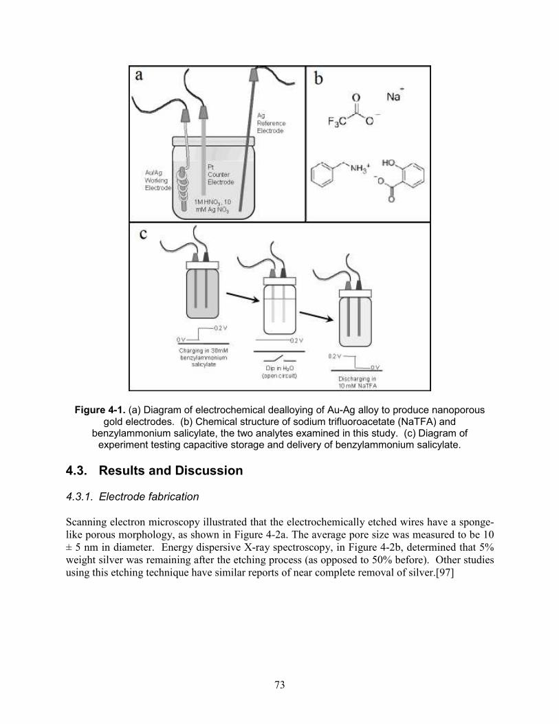
73
Figure 4-1. (a) Diagram of electrochemical dealloying of Au-Ag alloy to produce nanoporous gold electrodes. (b) Chemical structure of sodium trifluoroacetate (NaTFA) and
benzylammonium salicylate, the two analytes examined in this study. (c) Diagram of experiment testing capacitive storage and delivery of benzylammonium salicylate.
4.3. Results and Discussion 4.3.1. Electrode fabrication Scanning electron microscopy illustrated that the electrochemically etched wires have a sponge-like porous morphology, as shown in Figure 4-2a. The average pore size was measured to be 10 ± 5 nm in diameter. Energy dispersive X-ray spectroscopy, in Figure 4-2b, determined that 5% weight silver was remaining after the etching process (as opposed to 50% before). Other studies using this etching technique have similar reports of near complete removal of silver.[97]
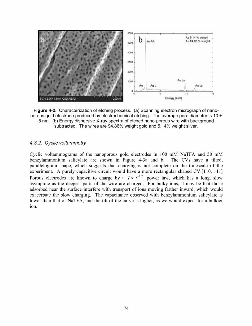
74
Figure 4-2. Characterization of etching process. (a) Scanning electron micrograph of nano-porous gold electrode produced by electrochemical etching. The average pore diameter is 10 ±
5 nm. (b) Energy dispersive X-ray spectra of etched nano-porous wire with background subtracted. The wires are 94.86% weight gold and 5.14% weight silver.
4.3.2. Cyclic voltammetry Cyclic voltammograms of the nanoporous gold electrodes in 100 mM NaTFA and 50 mM benzylammonium salicylate are shown in Figure 4-3a and b. The CVs have a tilted, parallelogram shape, which suggests that charging is not complete on the timescale of the experiment. A purely capacitive circuit would have a more rectangular shaped CV.[110, 111]
Porous electrodes are known to charge by a 2/1−∝ tI power law, which has a long, slow asymptote as the deepest parts of the wire are charged. For bulky ions, it may be that those adsorbed near the surface interfere with transport of ions moving farther inward, which would exacerbate the slow charging. The capacitance observed with benzylammonium salicylate is lower than that of NaTFA, and the tilt of the curve is higher, as we would expect for a bulkier ion.
75
Figure 4-3. Electrochemical characterization of nanoporous electrodes. (a) CV of 100 mM
NaTFA, (c) CV of 50 mM Benzylammonium salicylate at a 5 mV/s scan rate, (c) CA of 100 mM NaTFA with 100 mV and 200 mV applied, (d) CA of 50 mM benzylammonium salicylate with 100
mV and 200 mV applied.
We do not observe redox reactions or highly nonlinear capacitance in this range for these analytes. In voltammograms of other analytes, such as Fe(bipyridine)3SO4 and potassium aminobenzoate, we observed large current excursions indicative of redox reactions in certain voltage ranges. Since redox reactions can change the chemical identity of drugs, it is important to stay within a voltage range where redox does not occur. 4.3.3. Step height dependence The chronoamperometry responses of the electrodes in 100 mM NaTFA and 50 mM benzylammonium salicylate are presented in Figure 4-3c and d. The response with NaTFA is comparable to the exponential response of an ideal RC circuit, indicating that it becomes nearly fully charged on the timescale of the experiment. The total charge stored on the wire can be calculated by integrating the CA response. These values are presented in Table 4-2. As demonstrated in the CA response waveforms, applying higher voltages results in greater charge storage. Also, on the longer timescales of this experiment, the storage capacity was not dependent on the analyte.
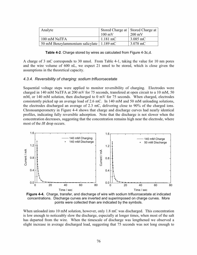
76
Analyte Stored Charge at
100 mV Stored Charge at 200 mV
100 mM NaTFA 1.181 mC 3.085 mC 50 mM Benzylammonium salicylate 1.189 mC 3.078 mC
Table 4-2. Charge stored by wires as calculated from Figure 4-3c,d.
A charge of 3 mC corresponds to 30 nmol. From Table 4-1, taking the value for 10 nm pores and the wire volume of 600 nL, we expect 21 nmol to be stored, which is close given the assumptions in the theoretical capacity. 4.3.4. Reversibility of charging: sodium trifluoroacetate Sequential voltage steps were applied to monitor reversibility of charging. Electrodes were charged in 140 mM NaTFA at 200 mV for 75 seconds, transfered at open circuit to a 10 mM, 50 mM, or 140 mM solution, then discharged to 0 mV for 75 seconds. When charged, electrodes consistently picked up an average load of 2.6 mC. In 140 mM and 50 mM unloading solutions, the electrodes discharged an average of 2.3 mC, delivering close to 90% of the charged ions. Chronoamperometry in Figure 4-4 shows that charge and discharge curves had nearly identical profiles, indicating fully reversible adsorption. Note that the discharge is not slower when the concentration decreases, suggesting that the concentration remains high near the electrode, where most of the IR drop occurs.
0 20 40 60 800.0
0.4
0.8
1.2
1.6
140 mM Charging
140 mM Discharge
Cu
rre
nt
/ m
A
Time / sec
0 20 40 60 800.0
0.4
0.8
1.2
1.6
140 mM Charge
50 mM Discharge
Cu
rre
nt
/ m
A
Time / sec Figure 4-4. Charge, transfer, and discharge of wire with sodium trifluoroacetate at indicated concentrations. Discharge curves are inverted and superimposed on charge curves. More
points were collected than are indicated by the symbols.
When unloaded into 10 mM solution, however, only 1.8 mC was discharged. This concentration is low enough to noticeably slow the discharge, especially at longer times, when most of the salt has departed from the wire. When the timescale of discharge was lengthened we observed a slight increase in average discharged load, suggesting that 75 seconds was not long enough to
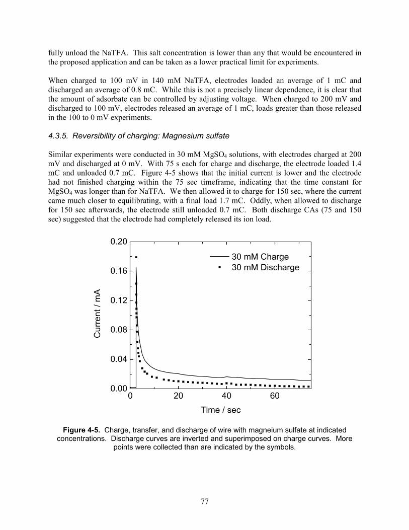
77
fully unload the NaTFA. This salt concentration is lower than any that would be encountered in the proposed application and can be taken as a lower practical limit for experiments. When charged to 100 mV in 140 mM NaTFA, electrodes loaded an average of 1 mC and discharged an average of 0.8 mC. While this is not a precisely linear dependence, it is clear that the amount of adsorbate can be controlled by adjusting voltage. When charged to 200 mV and discharged to 100 mV, electrodes released an average of 1 mC, loads greater than those released in the 100 to 0 mV experiments. 4.3.5. Reversibility of charging: Magnesium sulfate Similar experiments were conducted in 30 mM MgSO4 solutions, with electrodes charged at 200 mV and discharged at 0 mV. With 75 s each for charge and discharge, the electrode loaded 1.4 mC and unloaded 0.7 mC. Figure 4-5 shows that the initial current is lower and the electrode had not finished charging within the 75 sec timeframe, indicating that the time constant for MgSO4 was longer than for NaTFA. We then allowed it to charge for 150 sec, where the current came much closer to equilibrating, with a final load 1.7 mC. Oddly, when allowed to discharge for 150 sec afterwards, the electrode still unloaded 0.7 mC. Both discharge CAs (75 and 150 sec) suggested that the electrode had completely released its ion load.
0 20 40 600.00
0.04
0.08
0.12
0.16
0.20
30 mM Charge
30 mM Discharge
Cu
rre
nt
/ m
A
Time / sec
Figure 4-5. Charge, transfer, and discharge of wire with magneium sulfate at indicated concentrations. Discharge curves are inverted and superimposed on charge curves. More
points were collected than are indicated by the symbols.
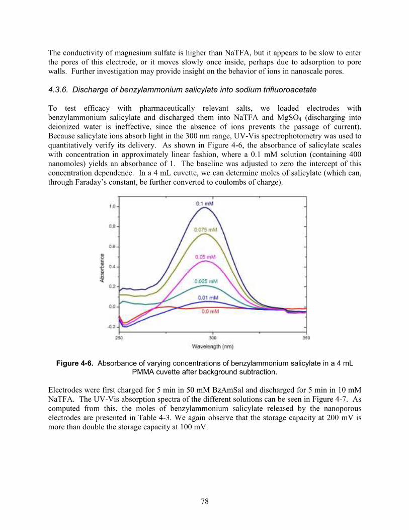
78
The conductivity of magnesium sulfate is higher than NaTFA, but it appears to be slow to enter the pores of this electrode, or it moves slowly once inside, perhaps due to adsorption to pore walls. Further investigation may provide insight on the behavior of ions in nanoscale pores. 4.3.6. Discharge of benzylammonium salicylate into sodium trifluoroacetate To test efficacy with pharmaceutically relevant salts, we loaded electrodes with benzylammonium salicylate and discharged them into NaTFA and MgSO4 (discharging into deionized water is ineffective, since the absence of ions prevents the passage of current). Because salicylate ions absorb light in the 300 nm range, UV-Vis spectrophotometry was used to quantitatively verify its delivery. As shown in Figure 4-6, the absorbance of salicylate scales with concentration in approximately linear fashion, where a 0.1 mM solution (containing 400 nanomoles) yields an absorbance of 1. The baseline was adjusted to zero the intercept of this concentration dependence. In a 4 mL cuvette, we can determine moles of salicylate (which can, through Faraday’s constant, be further converted to coulombs of charge).
Figure 4-6. Absorbance of varying concentrations of benzylammonium salicylate in a 4 mL
PMMA cuvette after background subtraction.
Electrodes were first charged for 5 min in 50 mM BzAmSal and discharged for 5 min in 10 mM NaTFA. The UV-Vis absorption spectra of the different solutions can be seen in Figure 4-7. As computed from this, the moles of benzylammonium salicylate released by the nanoporous electrodes are presented in Table 4-3. We again observe that the storage capacity at 200 mV is more than double the storage capacity at 100 mV.
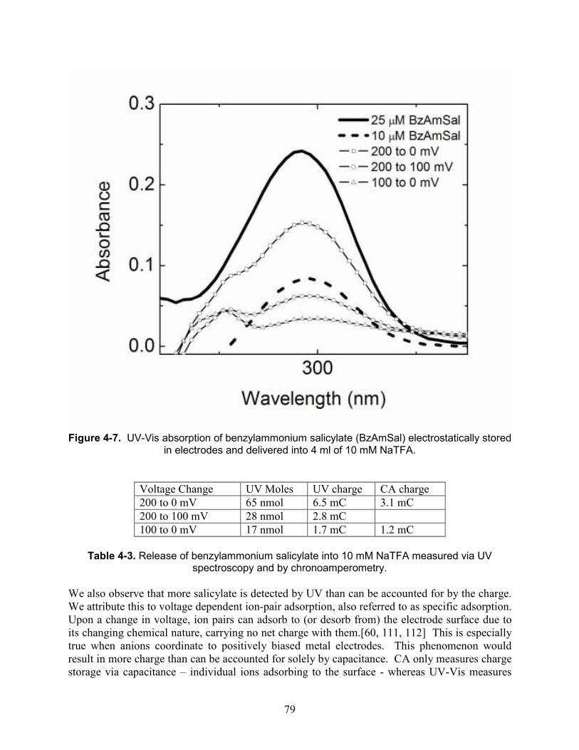
79
Figure 4-7. UV-Vis absorption of benzylammonium salicylate (BzAmSal) electrostatically stored
in electrodes and delivered into 4 ml of 10 mM NaTFA.
Voltage Change UV Moles UV charge CA charge 200 to 0 mV 65 nmol 6.5 mC 3.1 mC 200 to 100 mV 28 nmol 2.8 mC 100 to 0 mV 17 nmol 1.7 mC 1.2 mC
Table 4-3. Release of benzylammonium salicylate into 10 mM NaTFA measured via UV
spectroscopy and by chronoamperometry.
We also observe that more salicylate is detected by UV than can be accounted for by the charge. We attribute this to voltage dependent ion-pair adsorption, also referred to as specific adsorption. Upon a change in voltage, ion pairs can adsorb to (or desorb from) the electrode surface due to its changing chemical nature, carrying no net charge with them.[60, 111, 112] This is especially true when anions coordinate to positively biased metal electrodes. This phenomenon would result in more charge than can be accounted for solely by capacitance. CA only measures charge storage via capacitance – individual ions adsorbing to the surface - whereas UV-Vis measures
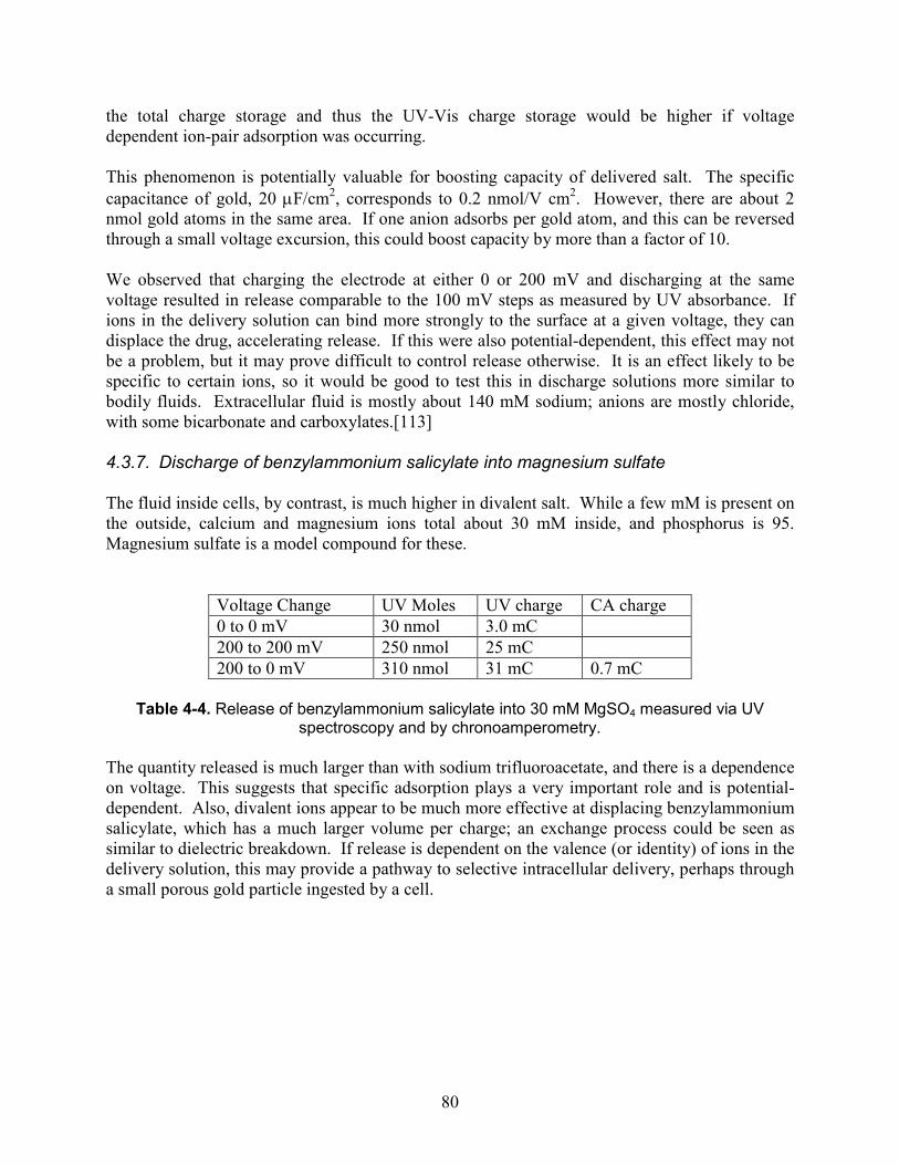
80
the total charge storage and thus the UV-Vis charge storage would be higher if voltage dependent ion-pair adsorption was occurring. This phenomenon is potentially valuable for boosting capacity of delivered salt. The specific capacitance of gold, 20 µF/cm2, corresponds to 0.2 nmol/V cm2. However, there are about 2 nmol gold atoms in the same area. If one anion adsorbs per gold atom, and this can be reversed through a small voltage excursion, this could boost capacity by more than a factor of 10. We observed that charging the electrode at either 0 or 200 mV and discharging at the same voltage resulted in release comparable to the 100 mV steps as measured by UV absorbance. If ions in the delivery solution can bind more strongly to the surface at a given voltage, they can displace the drug, accelerating release. If this were also potential-dependent, this effect may not be a problem, but it may prove difficult to control release otherwise. It is an effect likely to be specific to certain ions, so it would be good to test this in discharge solutions more similar to bodily fluids. Extracellular fluid is mostly about 140 mM sodium; anions are mostly chloride, with some bicarbonate and carboxylates.[113] 4.3.7. Discharge of benzylammonium salicylate into magnesium sulfate The fluid inside cells, by contrast, is much higher in divalent salt. While a few mM is present on the outside, calcium and magnesium ions total about 30 mM inside, and phosphorus is 95. Magnesium sulfate is a model compound for these.
Voltage Change UV Moles UV charge CA charge 0 to 0 mV 30 nmol 3.0 mC 200 to 200 mV 250 nmol 25 mC 200 to 0 mV 310 nmol 31 mC 0.7 mC
Table 4-4. Release of benzylammonium salicylate into 30 mM MgSO4 measured via UV
spectroscopy and by chronoamperometry.
The quantity released is much larger than with sodium trifluoroacetate, and there is a dependence on voltage. This suggests that specific adsorption plays a very important role and is potential-dependent. Also, divalent ions appear to be much more effective at displacing benzylammonium salicylate, which has a much larger volume per charge; an exchange process could be seen as similar to dielectric breakdown. If release is dependent on the valence (or identity) of ions in the delivery solution, this may provide a pathway to selective intracellular delivery, perhaps through a small porous gold particle ingested by a cell.
81
4.4. Conclusion The feasibility of electrically controlled delivery of charged pharmaceutical molecules by supercapacitors was demonstrated by charging and release of significant concentrations of relevant cations and anions. Electrochemically etched gold-silver alloy was an effective method to produce nanoporous electrodes that can be a test bed for this approach. Ion adsorption and desorption were found to be voltage dependent but non-linear, and storage capacity is augmented by specific adsorption of ion pairs. Ion exchange in the delivery solution can facilitate delivery, but possibly with loss of control. These phenomena are worthy of further study, as they may occur more or less – and be more or less potential-dependent – using different drugs or electrode materials. Examination of controlled loading and release of other pharmaceutically relevant molecules, particularly nucleic acids, is one promising area of future studies. In vitro and in vivo experiments are also needed to determine properties of molecule transport after desorption into tissue. With the potential to reduce cost and minimize pain and tissue damage, supercapacitive drug delivery is a promising addition to existing drug delivery methods.

82
[Blank page]
83
5. BIMODALLY POROUS ELECTRODE MATERIALS Experiments presented here were begun by Weon-Sik Chae with funding from this project
through the laboratory of Prof. Paul Braun at the University of Illinois. They were completed
with the assistance of Sung-Kyoung Ham after he moved to the Korea Basic Science Institute.
5.0. Abstract Nanoporous materials provide very high electrical energy storage capacity due to their high surface area in a given volume. However, ion transport hindrance through narrow nanopores typically slows down charging/discharging rates inside a bulk nanoporous device. In order to solve this problem, we have developed bimodally porous materials with opal architectures: narrow nanopores within spheres for electrical energy storage, and larger interstitial nanopores among spheres for charge transport, respectively. Two different concepts of material processing are used to fabricate two different nanoporous opals (carbon and gold) on gold electrodes. A triple templating route using a mesoporous silica phase creates bimodally nanoporous carbon. Alternatively, electroplating and dealloying processes in a silica inverse opal result in bimodally nanoporous gold. These unique nanoporous opaline materials will be used as a platform to develop more sophisticated nanoscale architectures for electrical energy storage devices. 5.1. Introduction Important technologies such as electrical energy storage, catalysis, and chemical separations depend on surface interactions. Nanoporous materials have the highest practical surface areas in a given volume, where every point in the material is within a small number of atoms of an interface. The disadvantage of these materials is that transport through long, narrow pores can be slow. For the case of capacitive energy storage, the charging time is proportional to L2/r, where L is the length and r is the radius of the pores.[8, 15] For fluid flow, the dependence on radius can be stronger, and in the electrical case, finite ion size relative to the pore radius and other nanoscale effects can restrict transport in the most narrow pores. Transport limitations could be alleviated if a network of wider pores penetrated a material with narrow pores.[114-116] For electrical storage, finely interpenetrated electrodes are desirable.[117] A simple implementation of a pore hierarchy could be a packed powder of nanoporous particles.[38] An optimal design would most likely involve an ordered arrangement of identical subunits. Such a design would also be easy to model, allowing experimental verification of design principles, and it may provide a useful step toward synthesis of interpenetrated structures. We present some new paths to ordered hierarchically nanoporous conductors that can help advance this effort. Specifically, we create opals of nanoporous gold and carbon. Gold containing a network of 10 nm pores can be prepared by stripping silver from silver-gold alloys.[20, 118-121] This has most often been in the form of films or foils, but some architectures with multiple designed size scales have been prepared.[122] Conducting porous carbon can be in the form of dense nanotube arrays or from high-temperature pyrolysis of carbon-rich precursors, including phenol-
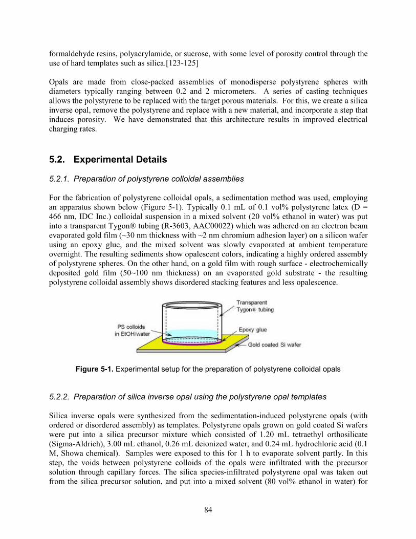
84
formaldehyde resins, polyacrylamide, or sucrose, with some level of porosity control through the use of hard templates such as silica.[123-125] Opals are made from close-packed assemblies of monodisperse polystyrene spheres with diameters typically ranging between 0.2 and 2 micrometers. A series of casting techniques allows the polystyrene to be replaced with the target porous materials. For this, we create a silica inverse opal, remove the polystyrene and replace with a new material, and incorporate a step that induces porosity. We have demonstrated that this architecture results in improved electrical charging rates. 5.2. Experimental Details 5.2.1. Preparation of polystyrene colloidal assemblies For the fabrication of polystyrene colloidal opals, a sedimentation method was used, employing an apparatus shown below (Figure 5-1). Typically 0.1 mL of 0.1 vol% polystyrene latex (D = 466 nm, IDC Inc.) colloidal suspension in a mixed solvent (20 vol% ethanol in water) was put into a transparent Tygon® tubing (R-3603, AAC00022) which was adhered on an electron beam evaporated gold film (~30 nm thickness with ~2 nm chromium adhesion layer) on a silicon wafer using an epoxy glue, and the mixed solvent was slowly evaporated at ambient temperature overnight. The resulting sediments show opalescent colors, indicating a highly ordered assembly of polystyrene spheres. On the other hand, on a gold film with rough surface - electrochemically deposited gold film (50~100 nm thickness) on an evaporated gold substrate - the resulting polystyrene colloidal assembly shows disordered stacking features and less opalescence.
Figure 5-1. Experimental setup for the preparation of polystyrene colloidal opals
5.2.2. Preparation of silica inverse opal using the polystyrene opal templates Silica inverse opals were synthesized from the sedimentation-induced polystyrene opals (with ordered or disordered assembly) as templates. Polystyrene opals grown on gold coated Si wafers were put into a silica precursor mixture which consisted of 1.20 mL tetraethyl orthosilicate (Sigma-Aldrich), 3.00 mL ethanol, 0.26 mL deionized water, and 0.24 mL hydrochloric acid (0.1 M, Showa chemical). Samples were exposed to this for 1 h to evaporate solvent partly. In this step, the voids between polystyrene colloids of the opals were infiltrated with the precursor solution through capillary forces. The silica species-infiltrated polystyrene opal was taken out from the silica precursor solution, and put into a mixed solvent (80 vol% ethanol in water) for
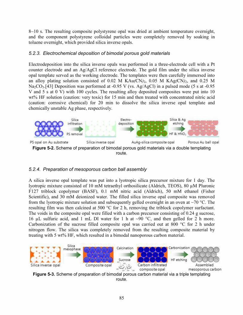
85
8~10 s. The resulting composite polystyrene opal was dried at ambient temperature overnight, and the component polystyrene colloidal particles were completely removed by soaking in toluene overnight, which provided silica inverse opals. 5.2.3. Electrochemical deposition of bimodal porous gold materials Electrodeposition into the silica inverse opals was performed in a three-electrode cell with a Pt counter electrode and an Ag/AgCl reference electrode. The gold film under the silica inverse opal template served as the working electrode. The templates were then carefully immersed into an alloy plating solution consisted of 0.02 M KAu(CN)2, 0.05 M KAg(CN)2, and 0.25 M Na2CO3.[43] Deposition was performed at -0.95 V (vs. Ag/AgCl) in a pulsed mode (5 s at -0.95 V and 5 s at 0 V) with 100 cycles. The resulting alloy deposited composites were put into 10 wt% HF solution (caution: very toxic) for 15 min and then treated with concentrated nitric acid (caution: corrosive chemical) for 20 min to dissolve the silica inverse opal template and chemically unstable Ag phase, respectively.
Figure 5-2. Scheme of preparation of bimodal porous gold materials via a double templating
route.
5.2.4. Preparation of mesoporous carbon ball assembly A silica inverse opal template was put into a lyotropic silica precursor mixture for 1 day. The lyotropic mixture consisted of 10 mM tetraethyl orthosilicate (Aldrich, TEOS), 80 µM Pluronic F127 triblock copolymer (BASF), 0.1 mM nitric acid (Aldrich), 50 mM ethanol (Fisher Scientific), and 30 mM deionized water. The filled silica inverse opal composite was removed from the lyotropic mixture solution and subsequently gelled overnight in an oven at ~70 °C. The resulting film was then calcined at 500 °C for 2 h, removing the triblock copolymer surfactant. The voids in the composite opal were filled with a carbon precursor consisting of 0.24 g sucrose, 16 µL sulfuric acid, and 1 mL DI water for 1 h at ~90 °C, and then gelled for 2 h more. Carbonization of the sucrose filled composite opal was carried out at 800 °C for 2 h under nitrogen flow. The silica was completely removed from the resulting composite material by treating with 5 wt% HF, which resulted in a bimodal nanoporous carbon material.
Figure 5-3. Scheme of preparation of bimodal porous carbon material via a triple templating
route.
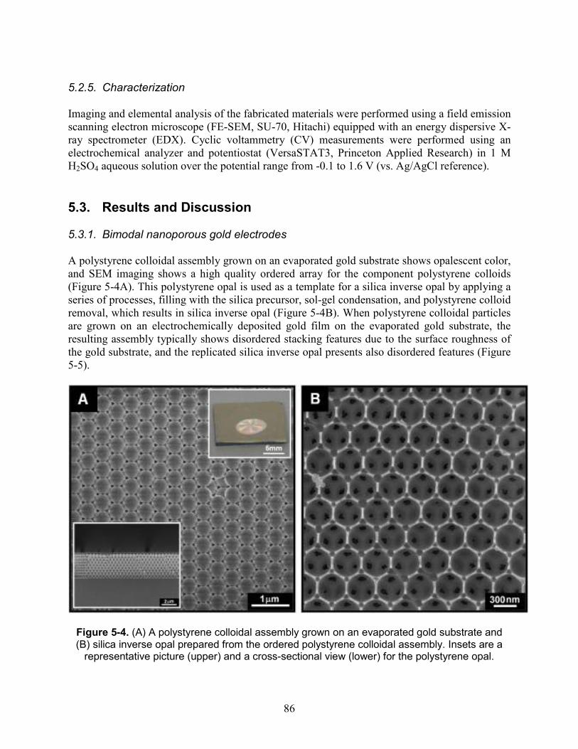
86
5.2.5. Characterization Imaging and elemental analysis of the fabricated materials were performed using a field emission scanning electron microscope (FE-SEM, SU-70, Hitachi) equipped with an energy dispersive X-ray spectrometer (EDX). Cyclic voltammetry (CV) measurements were performed using an electrochemical analyzer and potentiostat (VersaSTAT3, Princeton Applied Research) in 1 M H2SO4 aqueous solution over the potential range from -0.1 to 1.6 V (vs. Ag/AgCl reference). 5.3. Results and Discussion 5.3.1. Bimodal nanoporous gold electrodes A polystyrene colloidal assembly grown on an evaporated gold substrate shows opalescent color, and SEM imaging shows a high quality ordered array for the component polystyrene colloids (Figure 5-4A). This polystyrene opal is used as a template for a silica inverse opal by applying a series of processes, filling with the silica precursor, sol-gel condensation, and polystyrene colloid removal, which results in silica inverse opal (Figure 5-4B). When polystyrene colloidal particles are grown on an electrochemically deposited gold film on the evaporated gold substrate, the resulting assembly typically shows disordered stacking features due to the surface roughness of the gold substrate, and the replicated silica inverse opal presents also disordered features (Figure 5-5).
Figure 5-4. (A) A polystyrene colloidal assembly grown on an evaporated gold substrate and (B) silica inverse opal prepared from the ordered polystyrene colloidal assembly. Insets are a
representative picture (upper) and a cross-sectional view (lower) for the polystyrene opal.
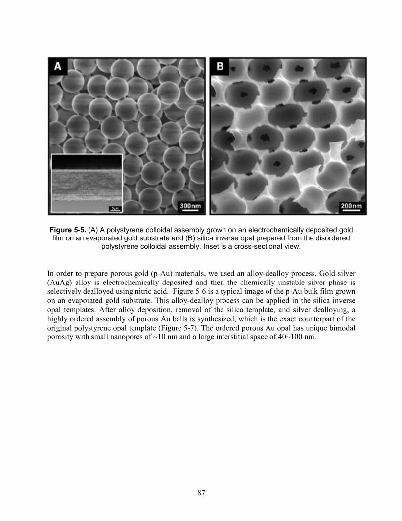
87
Figure 5-5. (A) A polystyrene colloidal assembly grown on an electrochemically deposited gold film on an evaporated gold substrate and (B) silica inverse opal prepared from the disordered
polystyrene colloidal assembly. Inset is a cross-sectional view.
In order to prepare porous gold (p-Au) materials, we used an alloy-dealloy process. Gold-silver (AuAg) alloy is electrochemically deposited and then the chemically unstable silver phase is selectively dealloyed using nitric acid. Figure 5-6 is a typical image of the p-Au bulk film grown on an evaporated gold substrate. This alloy-dealloy process can be applied in the silica inverse opal templates. After alloy deposition, removal of the silica template, and silver dealloying, a highly ordered assembly of porous Au balls is synthesized, which is the exact counterpart of the original polystyrene opal template (Figure 5-7). The ordered porous Au opal has unique bimodal porosity with small nanopores of ~10 nm and a large interstitial space of 40~100 nm.
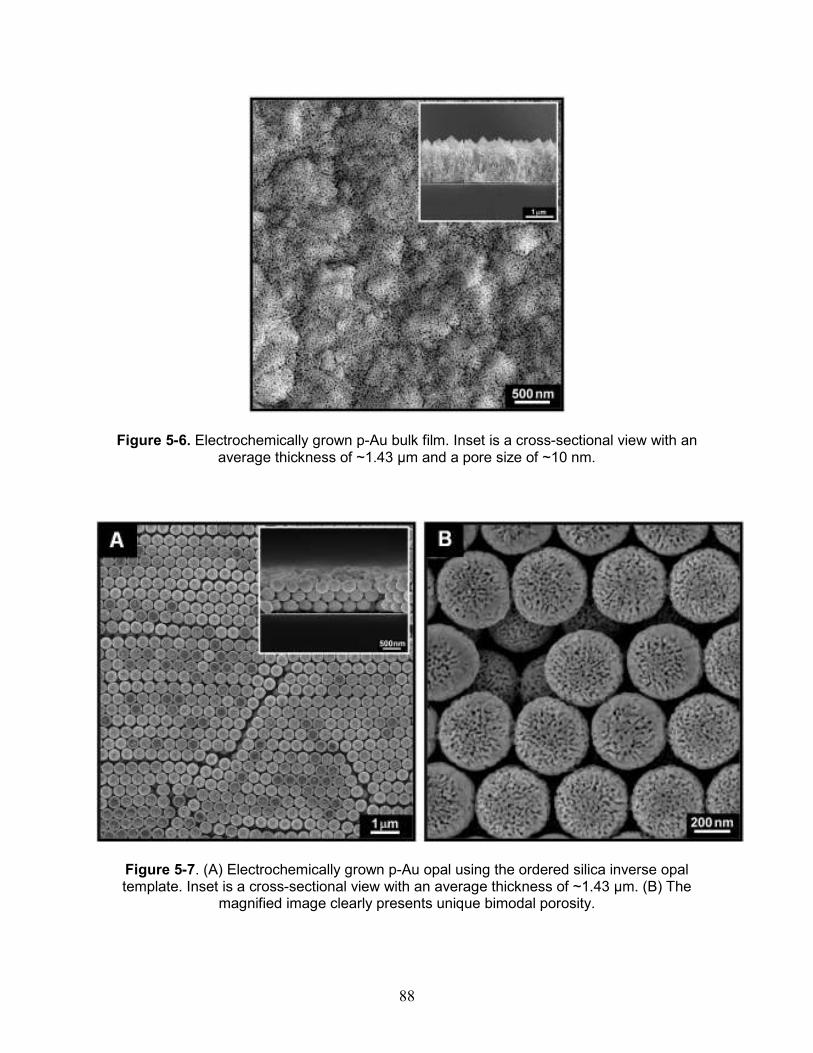
88
Figure 5-6. Electrochemically grown p-Au bulk film. Inset is a cross-sectional view with an average thickness of ~1.43 µm and a pore size of ~10 nm.
Figure 5-7. (A) Electrochemically grown p-Au opal using the ordered silica inverse opal template. Inset is a cross-sectional view with an average thickness of ~1.43 µm. (B) The
magnified image clearly presents unique bimodal porosity.
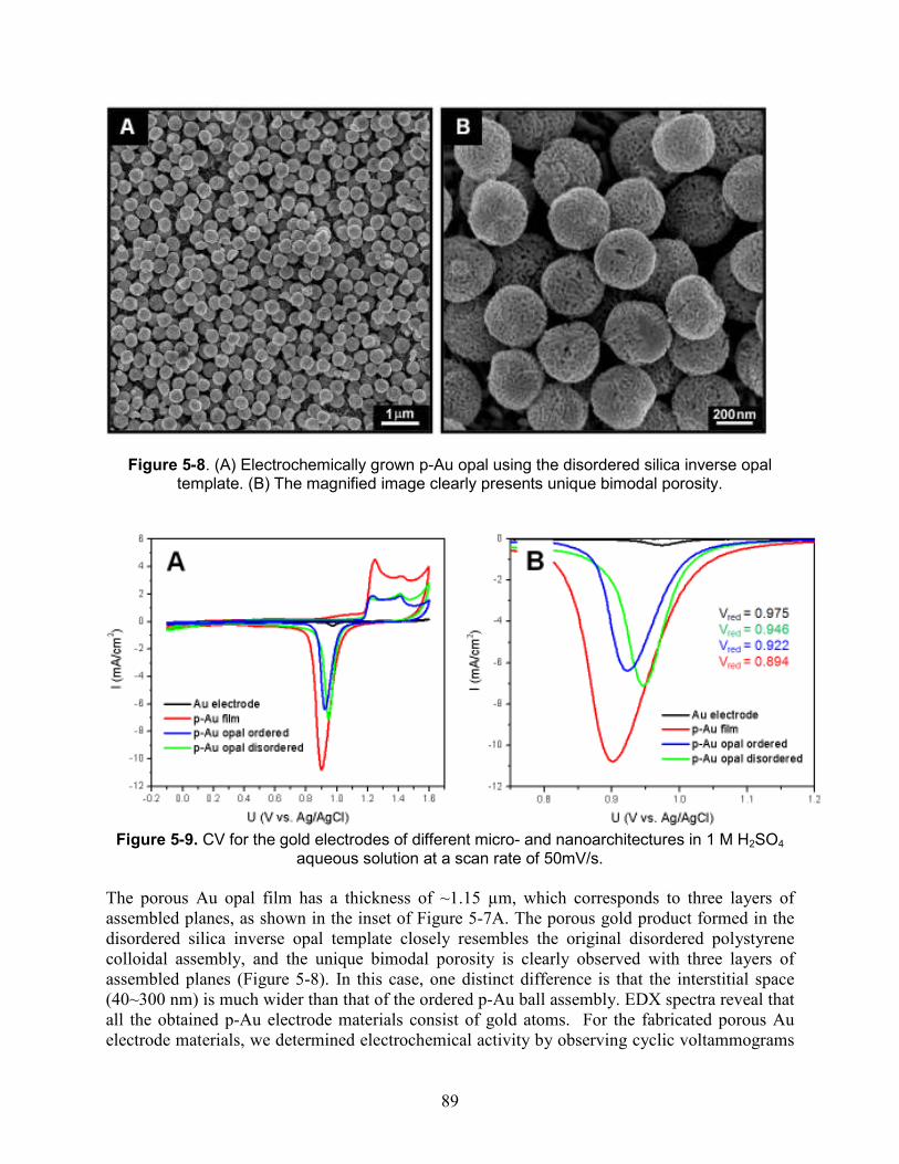
89
Figure 5-8. (A) Electrochemically grown p-Au opal using the disordered silica inverse opal template. (B) The magnified image clearly presents unique bimodal porosity.
Figure 5-9. CV for the gold electrodes of different micro- and nanoarchitectures in 1 M H2SO4
aqueous solution at a scan rate of 50mV/s.
The porous Au opal film has a thickness of ~1.15 µm, which corresponds to three layers of assembled planes, as shown in the inset of Figure 5-7A. The porous gold product formed in the disordered silica inverse opal template closely resembles the original disordered polystyrene colloidal assembly, and the unique bimodal porosity is clearly observed with three layers of assembled planes (Figure 5-8). In this case, one distinct difference is that the interstitial space (40~300 nm) is much wider than that of the ordered p-Au ball assembly. EDX spectra reveal that all the obtained p-Au electrode materials consist of gold atoms. For the fabricated porous Au electrode materials, we determined electrochemical activity by observing cyclic voltammograms
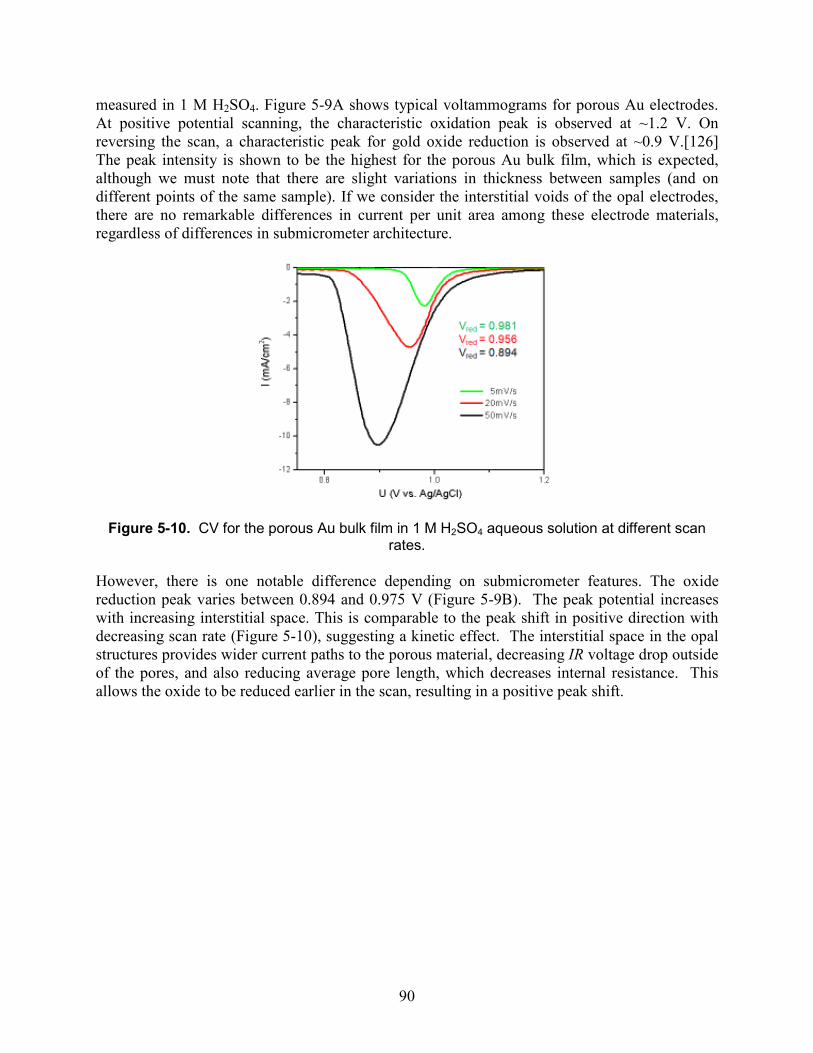
90
measured in 1 M H2SO4. Figure 5-9A shows typical voltammograms for porous Au electrodes. At positive potential scanning, the characteristic oxidation peak is observed at ~1.2 V. On reversing the scan, a characteristic peak for gold oxide reduction is observed at ~0.9 V.[126] The peak intensity is shown to be the highest for the porous Au bulk film, which is expected, although we must note that there are slight variations in thickness between samples (and on different points of the same sample). If we consider the interstitial voids of the opal electrodes, there are no remarkable differences in current per unit area among these electrode materials, regardless of differences in submicrometer architecture.
Figure 5-10. CV for the porous Au bulk film in 1 M H2SO4 aqueous solution at different scan rates.
However, there is one notable difference depending on submicrometer features. The oxide reduction peak varies between 0.894 and 0.975 V (Figure 5-9B). The peak potential increases with increasing interstitial space. This is comparable to the peak shift in positive direction with decreasing scan rate (Figure 5-10), suggesting a kinetic effect. The interstitial space in the opal structures provides wider current paths to the porous material, decreasing IR voltage drop outside of the pores, and also reducing average pore length, which decreases internal resistance. This allows the oxide to be reduced earlier in the scan, resulting in a positive peak shift.
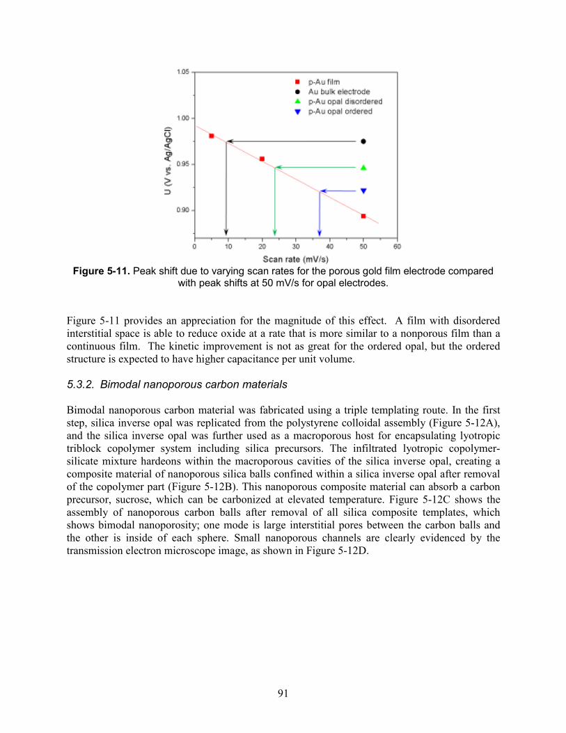
91
Figure 5-11. Peak shift due to varying scan rates for the porous gold film electrode compared
with peak shifts at 50 mV/s for opal electrodes.
Figure 5-11 provides an appreciation for the magnitude of this effect. A film with disordered interstitial space is able to reduce oxide at a rate that is more similar to a nonporous film than a continuous film. The kinetic improvement is not as great for the ordered opal, but the ordered structure is expected to have higher capacitance per unit volume. 5.3.2. Bimodal nanoporous carbon materials Bimodal nanoporous carbon material was fabricated using a triple templating route. In the first step, silica inverse opal was replicated from the polystyrene colloidal assembly (Figure 5-12A), and the silica inverse opal was further used as a macroporous host for encapsulating lyotropic triblock copolymer system including silica precursors. The infiltrated lyotropic copolymer-silicate mixture hardeons within the macroporous cavities of the silica inverse opal, creating a composite material of nanoporous silica balls confined within a silica inverse opal after removal of the copolymer part (Figure 5-12B). This nanoporous composite material can absorb a carbon precursor, sucrose, which can be carbonized at elevated temperature. Figure 5-12C shows the assembly of nanoporous carbon balls after removal of all silica composite templates, which shows bimodal nanoporosity; one mode is large interstitial pores between the carbon balls and the other is inside of each sphere. Small nanoporous channels are clearly evidenced by the transmission electron microscope image, as shown in Figure 5-12D.
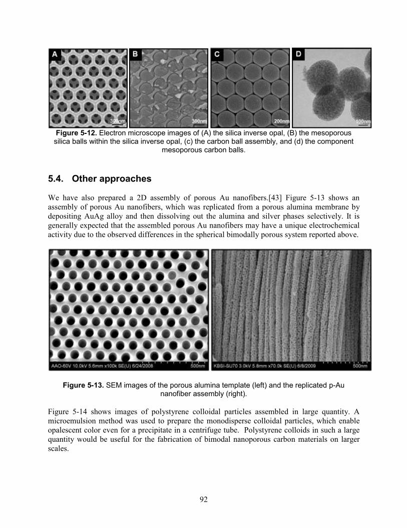
92
Figure 5-12. Electron microscope images of (A) the silica inverse opal, (B) the mesoporous silica balls within the silica inverse opal, (c) the carbon ball assembly, and (d) the component
mesoporous carbon balls.
5.4. Other approaches We have also prepared a 2D assembly of porous Au nanofibers.[43] Figure 5-13 shows an assembly of porous Au nanofibers, which was replicated from a porous alumina membrane by depositing AuAg alloy and then dissolving out the alumina and silver phases selectively. It is generally expected that the assembled porous Au nanofibers may have a unique electrochemical activity due to the observed differences in the spherical bimodally porous system reported above.
Figure 5-13. SEM images of the porous alumina template (left) and the replicated p-Au nanofiber assembly (right).
Figure 5-14 shows images of polystyrene colloidal particles assembled in large quantity. A microemulsion method was used to prepare the monodisperse colloidal particles, which enable opalescent color even for a precipitate in a centrifuge tube. Polystyrene colloids in such a large quantity would be useful for the fabrication of bimodal nanoporous carbon materials on larger scales.
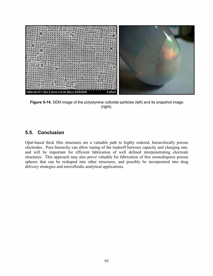
93
Figure 5-14. SEM image of the polystyrene colloidal particles (left) and its snapshot image (right).
5.5. Conclusion Opal-based thick film structures are a valuable path to highly ordered, hierarchically porous electrodes. Pore hierarchy can allow tuning of the tradeoff between capacity and charging rate, and will be important for efficient fabrication of well defined interpenetrating electrode structures. This approach may also prove valuable for fabrication of free monodisperse porous spheres that can be reshaped into other structures, and possibly be incorporated into drug delivery strategies and microfluidic analytical applications.

94
[Blank page]
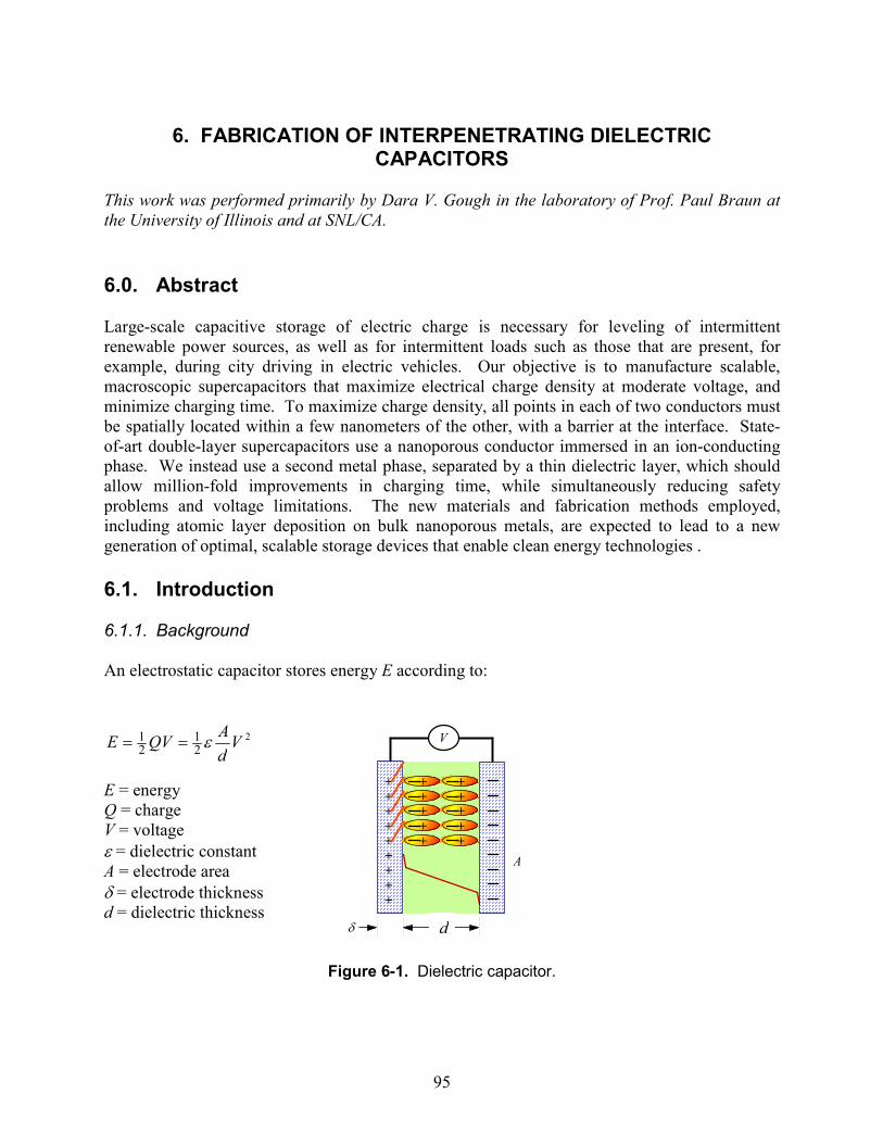
95
6. FABRICATION OF INTERPENETRATING DIELECTRIC CAPACITORS
This work was performed primarily by Dara V. Gough in the laboratory of Prof. Paul Braun at
the University of Illinois and at SNL/CA.
6.0. Abstract
Large-scale capacitive storage of electric charge is necessary for leveling of intermittent renewable power sources, as well as for intermittent loads such as those that are present, for example, during city driving in electric vehicles. Our objective is to manufacture scalable, macroscopic supercapacitors that maximize electrical charge density at moderate voltage, and minimize charging time. To maximize charge density, all points in each of two conductors must be spatially located within a few nanometers of the other, with a barrier at the interface. State-of-art double-layer supercapacitors use a nanoporous conductor immersed in an ion-conducting phase. We instead use a second metal phase, separated by a thin dielectric layer, which should allow million-fold improvements in charging time, while simultaneously reducing safety problems and voltage limitations. The new materials and fabrication methods employed, including atomic layer deposition on bulk nanoporous metals, are expected to lead to a new generation of optimal, scalable storage devices that enable clean energy technologies . 6.1. Introduction 6.1.1. Background An electrostatic capacitor stores energy E according to:
E = energy Q = charge V = voltage ε = dielectric constant A = electrode area δ = electrode thickness d = dielectric thickness
Figure 6-1. Dielectric capacitor.
2
21
21 V
d
AQVE ε==
L
+
+
+
+
+
+
+
+
+
A
+ +
+ +
+ +
+ +
+ +
V
δ d
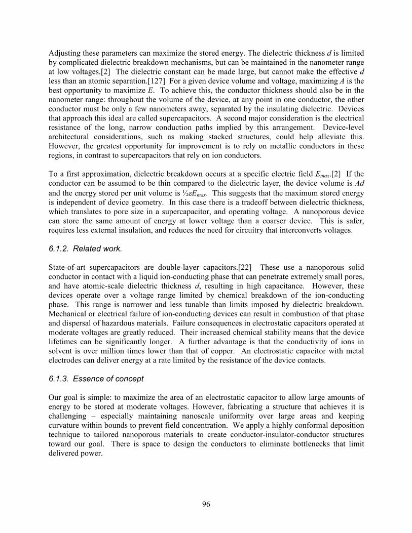
96
Adjusting these parameters can maximize the stored energy. The dielectric thickness d is limited by complicated dielectric breakdown mechanisms, but can be maintained in the nanometer range at low voltages.[2] The dielectric constant can be made large, but cannot make the effective d less than an atomic separation.[127] For a given device volume and voltage, maximizing A is the best opportunity to maximize E. To achieve this, the conductor thickness should also be in the nanometer range: throughout the volume of the device, at any point in one conductor, the other conductor must be only a few nanometers away, separated by the insulating dielectric. Devices that approach this ideal are called supercapacitors. A second major consideration is the electrical resistance of the long, narrow conduction paths implied by this arrangement. Device-level architectural considerations, such as making stacked structures, could help alleviate this. However, the greatest opportunity for improvement is to rely on metallic conductors in these regions, in contrast to supercapacitors that rely on ion conductors. To a first approximation, dielectric breakdown occurs at a specific electric field Emax.[2] If the conductor can be assumed to be thin compared to the dielectric layer, the device volume is Ad and the energy stored per unit volume is ½εEmax. This suggests that the maximum stored energy is independent of device geometry. In this case there is a tradeoff between dielectric thickness, which translates to pore size in a supercapacitor, and operating voltage. A nanoporous device can store the same amount of energy at lower voltage than a coarser device. This is safer, requires less external insulation, and reduces the need for circuitry that interconverts voltages. 6.1.2. Related work. State-of-art supercapacitors are double-layer capacitors.[22] These use a nanoporous solid conductor in contact with a liquid ion-conducting phase that can penetrate extremely small pores, and have atomic-scale dielectric thickness d, resulting in high capacitance. However, these devices operate over a voltage range limited by chemical breakdown of the ion-conducting phase. This range is narrower and less tunable than limits imposed by dielectric breakdown. Mechanical or electrical failure of ion-conducting devices can result in combustion of that phase and dispersal of hazardous materials. Failure consequences in electrostatic capacitors operated at moderate voltages are greatly reduced. Their increased chemical stability means that the device lifetimes can be significantly longer. A further advantage is that the conductivity of ions in solvent is over million times lower than that of copper. An electrostatic capacitor with metal electrodes can deliver energy at a rate limited by the resistance of the device contacts. 6.1.3. Essence of concept Our goal is simple: to maximize the area of an electrostatic capacitor to allow large amounts of energy to be stored at moderate voltages. However, fabricating a structure that achieves it is challenging – especially maintaining nanoscale uniformity over large areas and keeping curvature within bounds to prevent field concentration. We apply a highly conformal deposition technique to tailored nanoporous materials to create conductor-insulator-conductor structures toward our goal. There is space to design the conductors to eliminate bottlenecks that limit delivered power.
97
6.1.4. Substrate conductor A few methods are available that can be used to fabricate conductors that are nanoporous, and thus always have one interface within a few nanometers. Many involve thin film approaches,[117] requiring a uniform flux of precursors or etchants onto a thick planar substrate. Incremental efforts have led to impressive increases in the aspect ratios of these structures, and electrostatic capacitors have been fabricated by methods similar to those described here, but their scalability remains questionable, and thicker electrodes with higher conductivity are needed.[128] Porous carbon can be made through bulk sol-gel reactions,[129] which are scalable, and is the most common material used in double-layer supercapacitors. Carbon nanotube networks,[130] which are geometrically well defined and have higher conductivity and surface area, are now commercially produced in bulk reactors. A few nanoporous metals can be formed in bulk by etching less noble materials from alloys.[119, 131] A flexible route to bulk quantities of nanoporous metal and semiconductor powders is chemical reduction or precipitation in liquid crystals formed by concentrated aqueous surfactants.[19, 37, 38] Each of these is a promising substrate for fabrication of a bulk electrostatic supercapacitor, providing high surface area and satisfactory or tunable curvature. A few examples are shown in Figure 6-1.
Figure 6-2: Hierarchically porous carbon and gold, as described in the previous chapter, and porous platinum powders.[38]
6.1.5. Conformal dielectric layer To form an electrostatic capacitor, a perfectly conformal dielectric must be formed on the surface of one of these bulk nanoporous conductors, and then it must be backfilled with another conducting phase. The simplest approach to accomplish this is the growth of a self-terminating oxide layer, although this works best with electropositive materials that are not easily made nanoporous. The most conformal deposition procedure is atomic layer deposition, where in a single cycle vapor-phase reactants adsorb as monolayers, and are subsequently oxidized (or otherwise reacted); the cycles repeat until the desired film thickness is obtained. Some nanoporous metal substrates lose porosity at elevated temperature,[43] but alumina can be deposited at low temperatures (< 120 C). Alumina is a good insulator and can stabilize metal substrates against higher-temperature subsequent steps, such as deposition of titanates with higher dielectric constants. Oxide deposition on porous carbon has also been demonstrated.[132] We will use alumina to seal off areas of anomalous negative curvature to prevent field concentration.
50nm
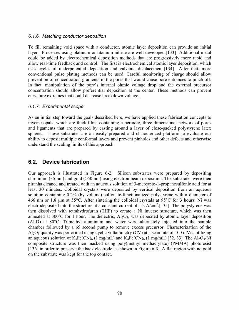
98
6.1.6. Matching conductor deposition To fill remaining void space with a conductor, atomic layer deposition can provide an initial layer. Processes using platinum or titanium nitride are well developed.[133] Additional metal could be added by electrochemical deposition methods that are progressively more rapid and allow real-time feedback and control. The first is electrochemical atomic layer deposition, which uses cycles of underpotential deposition and galvanic displacement.[134] After that, more conventional pulse plating methods can be used. Careful monitoring of charge should allow prevention of concentration gradients in the pores that would cause pore entrances to pinch off. In fact, manipulation of the pore’s internal ohmic voltage drop and the external precursor concentration should allow preferential deposition at the center. These methods can prevent curvature extremes that could decrease breakdown voltage.
6.1.7. Experimental scope As an initial step toward the goals described here, we have applied these fabrication concepts to inverse opals, which are thick films containing a periodic, three-dimensional network of pores and ligaments that are prepared by casting around a layer of close-packed polystyrene latex spheres. These substrates are an easily prepared and characterized platform to evaluate our ability to deposit multiple conformal layers and prevent pinholes and other defects and otherwise understand the scaling limits of this approach. 6.2. Device fabrication Our approach is illustrated in Figure 6-2. Silicon substrates were prepared by depositing chromium (~5 nm) and gold (>50 nm) using electron beam deposition. The substrates were then piranha cleaned and treated with an aqueous solution of 3-mercapto-1-propanesulfonic acid for at least 30 minutes. Colloidal crystals were deposited by vertical deposition from an aqueous solution containing 0.2% (by volume) sulfonate-functionalized polystyrene with a diameter of 466 nm or 1.8 µm at 55°C. After sintering the colloidal crystals at 95°C for 3 hours, Ni was electrodeposited into the structure at a constant current of 1.2 A/cm2.[135] The polystyrene was then dissolved with tetrahydrofuran (THF) to create a Ni inverse structure, which was then annealed at 300oC for 1 hour. The dielectric, Al2O3, was deposited by atomic layer deposition (ALD) at 80°C. Trimethyl aluminum and water were alternately injected into the sample chamber followed by a 65 second pump to remove excess precursor. Characterization of the Al2O3 quality was performed using cyclic voltammetry (CV) at a scan rate of 100 mV/s, utilizing an aqueous solution of K3Fe(CN)6 (1 mg/mL) and K4Fe(CN)6 (1 mg/mL).[32, 33] The Al2O3-Ni composite structure was then masked using poly(methyl methacrylate) (PMMA) photoresist [136] in order to preserve the back electrode, as shown in Figure 6-3. A flat region with no gold on the substrate was kept for the top contact.
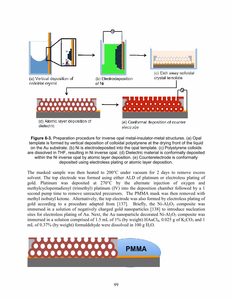
99
Figure 6-3. Preparation procedure for inverse opal metal-insulator-metal structures. (a) Opal
template is formed by vertical deposition of colloidal polystyrene at the drying front of the liquid on the Au substrate. (b) Ni is electrodeposited into the opal template. (c) Polystyrene colloids
are dissolved in THF, resulting in Ni inverse opal. (d) Dielectric material is conformally deposited within the Ni inverse opal by atomic layer deposition. (e) Counterelectrode is conformally
deposited using electroless plating or atomic layer deposition.
The masked sample was then heated to 200°C under vacuum for 2 days to remove excess solvent. The top electrode was formed using either ALD of platinum or electroless plating of gold. Platinum was deposited at 270°C by the alternate injection of oxygen and methylcyclopentadienyl (trimethyl) platinum (IV) into the deposition chamber followed by a 1 second pump time to remove unreacted precursors. The PMMA mask was then removed with methyl isobutyl ketone. Alternatively, the top electrode was also formed by electroless plating of gold according to a procedure adapted from [137]. Briefly, the Ni-Al2O3 composite was immersed in a solution of negatively charged gold nanoparticles [138] to introduce nucleation sites for electroless plating of Au. Next, the Au nanoparticle decorated Ni-Al2O3 composite was immersed in a solution comprised of 1.5 mL of 1% (by weight) HAuCl4, 0.025 g of K2CO3 and 1 mL of 0.37% (by weight) formaldehyde were dissolved in 100 g H2O.
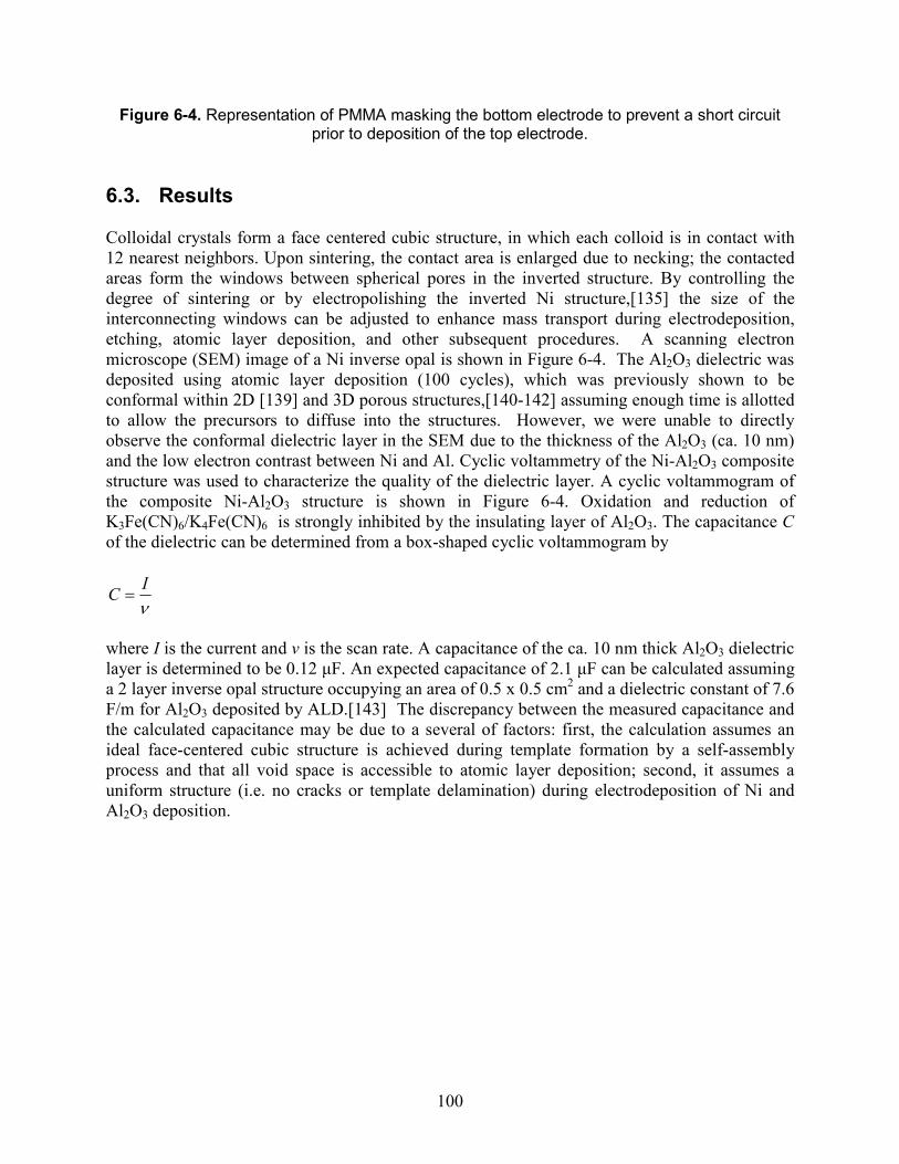
100
Figure 6-4. Representation of PMMA masking the bottom electrode to prevent a short circuit prior to deposition of the top electrode.
6.3. Results Colloidal crystals form a face centered cubic structure, in which each colloid is in contact with 12 nearest neighbors. Upon sintering, the contact area is enlarged due to necking; the contacted areas form the windows between spherical pores in the inverted structure. By controlling the degree of sintering or by electropolishing the inverted Ni structure,[135] the size of the interconnecting windows can be adjusted to enhance mass transport during electrodeposition, etching, atomic layer deposition, and other subsequent procedures. A scanning electron microscope (SEM) image of a Ni inverse opal is shown in Figure 6-4. The Al2O3 dielectric was deposited using atomic layer deposition (100 cycles), which was previously shown to be conformal within 2D [139] and 3D porous structures,[140-142] assuming enough time is allotted to allow the precursors to diffuse into the structures. However, we were unable to directly observe the conformal dielectric layer in the SEM due to the thickness of the Al2O3 (ca. 10 nm) and the low electron contrast between Ni and Al. Cyclic voltammetry of the Ni-Al2O3 composite structure was used to characterize the quality of the dielectric layer. A cyclic voltammogram of the composite Ni-Al2O3 structure is shown in Figure 6-4. Oxidation and reduction of K3Fe(CN)6/K4Fe(CN)6 is strongly inhibited by the insulating layer of Al2O3. The capacitance C of the dielectric can be determined from a box-shaped cyclic voltammogram by
νI
C =
where I is the current and ν is the scan rate. A capacitance of the ca. 10 nm thick Al2O3 dielectric layer is determined to be 0.12 µF. An expected capacitance of 2.1 µF can be calculated assuming a 2 layer inverse opal structure occupying an area of 0.5 x 0.5 cm2 and a dielectric constant of 7.6 F/m for Al2O3 deposited by ALD.[143] The discrepancy between the measured capacitance and the calculated capacitance may be due to a several of factors: first, the calculation assumes an ideal face-centered cubic structure is achieved during template formation by a self-assembly process and that all void space is accessible to atomic layer deposition; second, it assumes a uniform structure (i.e. no cracks or template delamination) during electrodeposition of Ni and Al2O3 deposition.
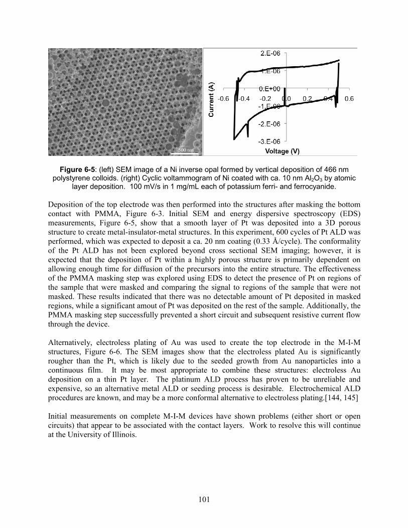
101
Figure 6-5: (left) SEM image of a Ni inverse opal formed by vertical deposition of 466 nm polystyrene colloids. (right) Cyclic voltammogram of Ni coated with ca. 10 nm Al2O3 by atomic
layer deposition. 100 mV/s in 1 mg/mL each of potassium ferri- and ferrocyanide.
Deposition of the top electrode was then performed into the structures after masking the bottom contact with PMMA, Figure 6-3. Initial SEM and energy dispersive spectroscopy (EDS) measurements, Figure 6-5, show that a smooth layer of Pt was deposited into a 3D porous structure to create metal-insulator-metal structures. In this experiment, 600 cycles of Pt ALD was performed, which was expected to deposit a ca. 20 nm coating (0.33 Å/cycle). The conformality of the Pt ALD has not been explored beyond cross sectional SEM imaging; however, it is expected that the deposition of Pt within a highly porous structure is primarily dependent on allowing enough time for diffusion of the precursors into the entire structure. The effectiveness of the PMMA masking step was explored using EDS to detect the presence of Pt on regions of the sample that were masked and comparing the signal to regions of the sample that were not masked. These results indicated that there was no detectable amount of Pt deposited in masked regions, while a significant amout of Pt was deposited on the rest of the sample. Additionally, the PMMA masking step successfully prevented a short circuit and subsequent resistive current flow through the device. Alternatively, electroless plating of Au was used to create the top electrode in the M-I-M structures, Figure 6-6. The SEM images show that the electroless plated Au is significantly rougher than the Pt, which is likely due to the seeded growth from Au nanoparticles into a continuous film. It may be most appropriate to combine these structures: electroless Au deposition on a thin Pt layer. The platinum ALD process has proven to be unreliable and expensive, so an alternative metal ALD or seeding process is desirable. Electrochemical ALD procedures are known, and may be a more conformal alternative to electroless plating.[144, 145] Initial measurements on complete M-I-M devices have shown problems (either short or open circuits) that appear to be associated with the contact layers. Work to resolve this will continue at the University of Illinois.
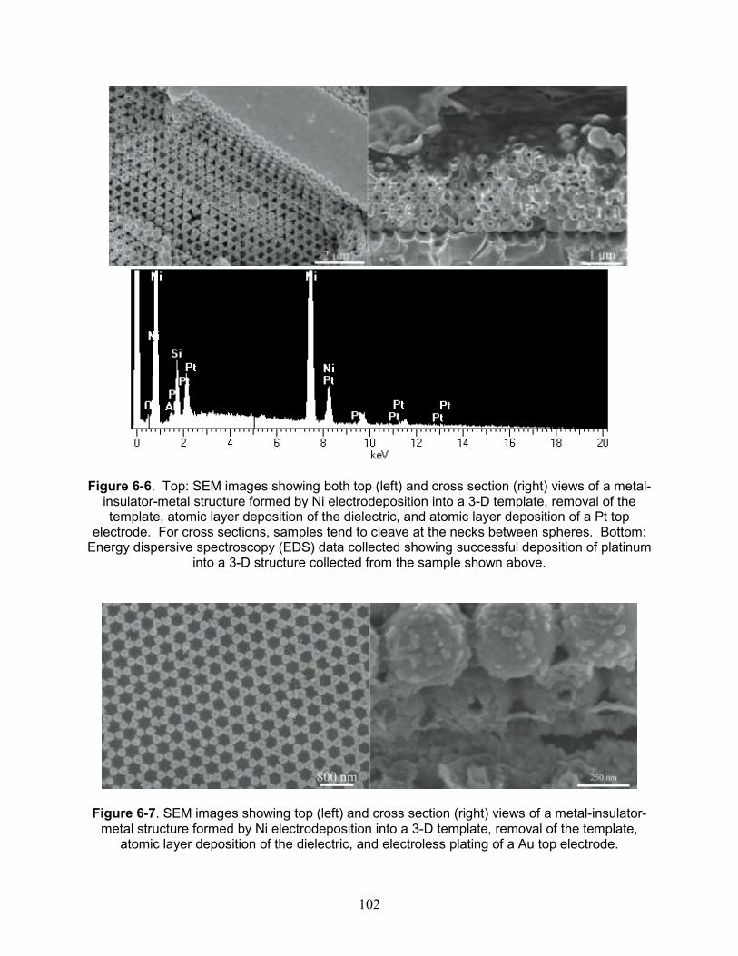
102
Figure 6-6. Top: SEM images showing both top (left) and cross section (right) views of a metal-insulator-metal structure formed by Ni electrodeposition into a 3-D template, removal of the template, atomic layer deposition of the dielectric, and atomic layer deposition of a Pt top
electrode. For cross sections, samples tend to cleave at the necks between spheres. Bottom: Energy dispersive spectroscopy (EDS) data collected showing successful deposition of platinum
into a 3-D structure collected from the sample shown above.
Figure 6-7. SEM images showing top (left) and cross section (right) views of a metal-insulator-
metal structure formed by Ni electrodeposition into a 3-D template, removal of the template, atomic layer deposition of the dielectric, and electroless plating of a Au top electrode.
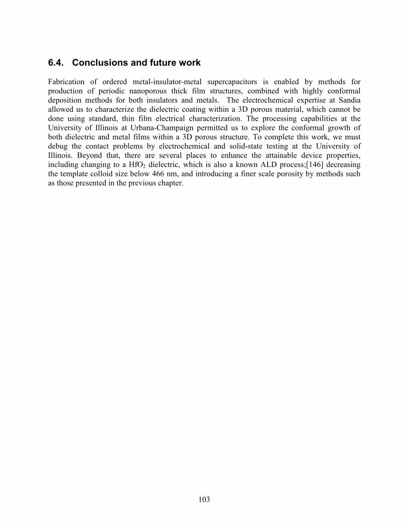
103
6.4. Conclusions and future work Fabrication of ordered metal-insulator-metal supercapacitors is enabled by methods for production of periodic nanoporous thick film structures, combined with highly conformal deposition methods for both insulators and metals. The electrochemical expertise at Sandia allowed us to characterize the dielectric coating within a 3D porous material, which cannot be done using standard, thin film electrical characterization. The processing capabilities at the University of Illinois at Urbana-Champaign permitted us to explore the conformal growth of both dielectric and metal films within a 3D porous structure. To complete this work, we must debug the contact problems by electrochemical and solid-state testing at the University of Illinois. Beyond that, there are several places to enhance the attainable device properties, including changing to a HfO2 dielectric, which is also a known ALD process;[146] decreasing the template colloid size below 466 nm, and introducing a finer scale porosity by methods such as those presented in the previous chapter.

104
[Blank page]
105
7. FUTURE OPPORTUNITIES FOR SUPERCAPACITORS
7.1. Background Supercapacitors use electrostatic charge or fast, reversible interfacial redox reactions to achieve higher power densities than batteries, complementing them in an energy storage system. They can extend range and boost acceleration of electrified vehicles by recovering and delivering energy inaccessible to batteries during speed changes and rapid recharge opportunities. The same effects can reduce capital costs of intermittent renewable energy harvesting applications. These are necessary steps for market acceptance of technologies required for energy independence. These devices maximize charge stored at a prescribed voltage by maximizing area and minimizing thickness of the interface. The practical physical extreme of this is a nanoporous electrode, where every point in the conductor is within a few nanometers of an interface, and where one phase is a salt-containing liquid, so charge carriers can be atomically close to a metallic electrode. To boost power density, the pore aspect ratio and spacing between electrodes must be kept as low as possible. Ideally, each electrode would interpenetrate the other’s pores, without making electrical contact. In practice, there will be a crossover scale where charge goes from being carried by electrodes to the electrolyte. Furthermore, as noted elsewhere in this proposal, surpluses in power density can be translated into gains in energy density. This scale is currently far from its optimum in existing devices – typically hundreds of micrometers. Furthermore, optimal performance can likely be improved with a greater understanding of ion transport behavior in nanoscale pores, an area where many open questions remain. Sandia capabilities in fabrication, characterization, and modeling will enable an approach that, with proper focus, could allow rapid progress toward that point comparable to that enjoyed during optimization of integrated circuits by Moore’s Law.
7.2. Ion behavior in nanoporous supercapacitor electrodes Classical models can adequately describe ion transport in micrometer-scale pores, but these break down in nanometer-scale pores, where the equilibrium electrostatic charge and the amount of chemisorbed salt can exceed that available from the dissolved salt in the pores – two effects that can counteract each other. Pore diameter is comparable to predicted diffuse layer thicknesses; the implications of this are controversial. The discrete width of ions and solvent molecules becomes a consideration, and wall interactions can prevent or enhance entry of ions into a pore. Study of these issues would provide a complete understanding of ion behavior relevant to pore charging, and lead to development of lumped element models that incorporate that behavior to enable device design that take full advantage of predicted phenomena. Application of density functional theory by Bob Nilson, Amalie Frischknecht, Susan Rempe, and others would generate a thorough understanding of discrete solvation effects on ion mobility and
106
chemical potential within a conducting pore, and determine ways to optimize it by modifying wall interactions with ions and solvent. They could determine the contribution to charging of lateral transport of specifically adsorbed salt, and the contribution to conductivity of desorbed and diffuse-layer ions. General analytical approximations resulting from these that apply to finite voltages and temperatures would be of great value in device modeling. Atomistic models will be validated on nanoporous electrode test platforms, such as those described in this report: easily characterized tunable, regular pore arrays that conform to simplifying assumptions made in modeling efforts. These include surfactant-templated platinum group metal films; thiol monolayer-functionalized, dealloyed gold; and perhaps also vertical carbon nanotube arrays. For studies of pseudocapacitance, redox-active organic monolayers, or nanoparticle arrays will be applied, the latter approach proposed by Todd Munson. In addition to standard electrochemical impedance and voltammetry studies, John Sullivan, Jianyu Huang and Roger Farrow have invented in situ analysis tools to interrogate ion behavior at the single-pore level and below. Nancy Missert’s electrochemical scanning probe microscopy capabilities would allow mapping of ion partitioning, neighboring pore crosstalk, and their effects on charging rates. To observe spatial dependence of salt depletion, facing pairs of high aspect ratio grating electrodes could be incorporated into the TEM electrochemical cell under development by Sullivan and Huang, and charging observed using a high-Z salt such as cesium iodide. Optical and X-ray methods could quantify adsorbed and diffuse salt as a function of potential, surface chemistry, and pore size in electrodes. These efforts would result in experimentally verified mathematical descriptions of ion behavior in nanoscale pores that will be usable for device design.
7.3. Achieving physical limits of supercapacitor performance Detailed understanding of nanopore charging behavior would allow us to design, fabricate, and evaluate device structures that make optimal use of it, making best use of available approaches and charting a path forward when new approaches become available and demand is created for large-scale manufacturing of supercapacitors. Nilson and Stewart Griffiths have been developing device-level transport models that include behavior of pore charging. Further work is needed to prescribe architectural approaches and scales that account for thermal and mechanical stability constraints and heat dissipation needs for anticipated material choices, operating conditions, and fabrication capabilities. This must consider form factors relevant to anticipated applications, including interconnects. Attention must be paid to scalability of their designs, mitigating slow mass transport during fabrication steps to allow high throughput. A device material development group that could include Dale Huber, Hongyou Fan, John Shelnutt, and others in addition to the authors could pursue the creation of these architectures first using materials that are most likely to allow model validation and meet performance targets. As these are achieved, focus would turn to use of more scalable, cost-effective materials.
107
To create devices with interpenetrating nanoporous electrodes, this work would begin with a highly ordered and well understood electrode as described in the Ion Behavior effort. We then must apply a highly conformal separator that conducts ions but not electrons, and will prevent short circuits or high field concentration. This will require layer-by-layer fabrication, such as atomic layer deposition of solid oxides that conduct ions, step-growth polymerization, or careful polymer grafting. A conformal conducting layer must then be applied, again using vapor or electrochemical atomic layer deposition, or chemical seeding. To ensure adequate conductance of the second electrode, the remaining volume must be backfilled with conducting material by coarser methods such as electroplating. This approach would bring us to a realm near the anticipated physical limits of power density in a supercapacitor, taking full advantage of the entire volume of the material. To boost the energy density and cost effectiveness of these devices, a parallel effort would apply new materials to the prescribed architecture. Porous carbon is cost effective and can be made with very small pores and high surface areas. However, because its fabrication requires high temperatures, controlling pore architecture, conductivity, and other material properties is challenging. Recent developments in porous carbon synthesis by Fan and at Oak Ridge National Laboratory present opportunities to achieve this control. Transition metal oxide coatings and electrodes developed by Bruce Bunker, Erik Spoerke, and others at Sandia and Lawrence Livermore National Laboratory allow fast, reversible redox charging in a pore, resulting in possible tenfold improvements in energy density; it would be fruitful to apply expertise toward integration of these materials. Conducting polymers may find application in the finer structures of the second electrode, which could reduce fabrication cost. The properties of devices and individual electrodes will be characterized by electrochemical methods, electron microscopy, porosimetry, and other methods throughout this work in order to validate models and demonstrate progress in device performance. Fully characterized functional prototypes are within the scope of Sandia’s capabilities, as would be complete design guidelines for further advancement of the energy storage equivalent of Moore’s Law. 7.4. Impact on DOE mission
The optimization of energy generation, storage and transmission represents perhaps the greatest global obstacle to successful environmental stewardship and geopolitical stability. In fact, successful implementation of available technologies that increase efficiency, reduce dependence on foreign energy sources, and reduce greenhouse emissions has been hindered by their ability to match generation and load. To that effect, successful development of optimized supercapacitors will be transformational by enabling a wide range of renewable energy applications, as well as improvements in other storage devices such as batteries and fuel cells. 7.4.1. Transportation applications Internal combustion engines in conventional and hybrid cars and buses rarely perform at their cleanest and most efficient operating conditions. Energy is mostly dissipated during braking because it cannot be recovered rapidly and efficiently stored. Energy losses due to these factors
108
increase fuel consumption per mile by tens of percentage points. Improvements in this range could be significant as they could help reach a threshold point where efficient vehicle technologies become widely adopted by the marketplace, such as an all-electric vehicle that offers competitive range and power. A supercapacitor that could capture energy in a compact form with minimal ohmic heating during braking and rapidly return it to the drivetrain during acceleration would make such a contribution. This technology could also be applied to grid-wired electric vehicles such as commuter and light rail systems that currently dissipate much of their braking energy, providing opportunity for reduction of the financial and environmental cost of public transportation, and increasing its use. A 1000 kg vehicle requires 3x10⁵ J or about 90 Wh to accelerate to 55 mph, so a target energy density for a device is about 10 Wh/kg, resulting in a device comparable to a standard car battery. This should fully charge in about 1 second to ensure that ohmic losses do not inhibit energy capture, requiring a power density of 3x10⁴ W/kg. Such a device could deliver a 20 mph boost in a comparable time for passing on a highway; such power often trumps efficiency in the marketplace. Devices useful in personal vehicles would also be of value in rail vehicles and buses. 7.4.2. Renewable electricity applications An additional, potentially transformational application of electrostatic supercapacitors, involves load balancing of intermittent renewable energy sources such as wind and solar electricity generation. Current solutions include pumping water uphill, which is low energy density (less than 0.1 Wh/kg). Molten salt storage can be high energy density (100 Wh/kg) but power density is low and plant costs are high. It is likely that the marginal cost per kg for capacitors will be much higher than these other methods, but they can probably apply to smaller remote power systems where renewable sources are already in common use. 7.4.3. Impact on energy-related fields Our proposed supercapacitor architectures access uncharted territory on a frequently cited power-vs.-energy plot showing the roles of different electrical energy storage devices (Figure 7-1). With the equation and [2], the ideal energy density of an alumina electrostatic capacitor is 1 Wh/kg, assuming half of the mass is electrode, no packaging, and that the density of everything is 3 g/cm3. The bandwidth of a typical ceramic capacitor is 50 MHz, corresponding to a 3 ns time constant and a 1012 W/kg power density. This is for a 1 kV capacitor, and there is a tradeoff between maximum operating voltage and bandwidth. An ideal number for a low-voltage capacitor would be 109 W/kg. Dielectric capacitors that use high-permittivity insulators, such as barium or strontium titanate, can increase the amount of charge stored by a factor of 10. If this allows access to the 10 Wh/kg range, it would be practical to use electrostatic capacitors in vehicles. Because these materials reduce the effective dielectric thickness L/ε to atomic dimensions, we expect this to be a firm upper limit. Real capacitors are mostly packaging and electrodes, which can reduce these numbers by a factor of ten. Real electrolytic capacitors, which contain an ion conductor in series with a dielectric film, can have power densities of 3x10⁴ W/kg and energy densities of 0.1 Wh/kg.
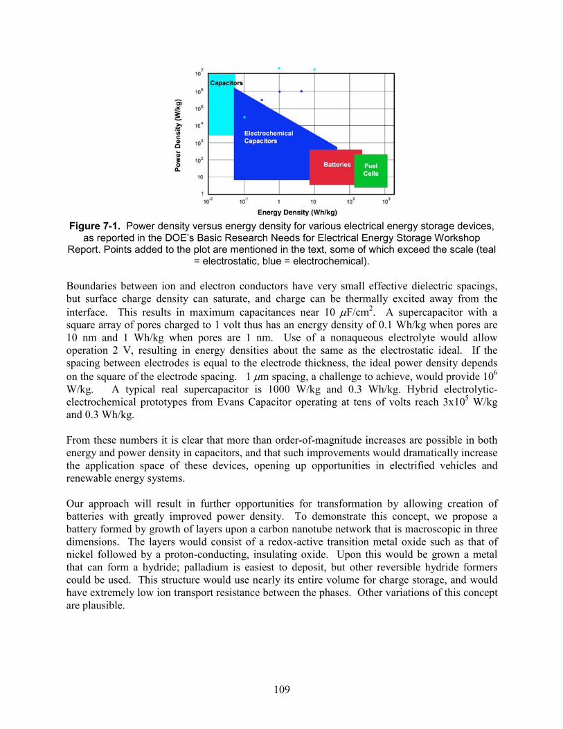
109
Figure 7-1. Power density versus energy density for various electrical energy storage devices,
as reported in the DOE’s Basic Research Needs for Electrical Energy Storage Workshop Report. Points added to the plot are mentioned in the text, some of which exceed the scale (teal
= electrostatic, blue = electrochemical).
Boundaries between ion and electron conductors have very small effective dielectric spacings, but surface charge density can saturate, and charge can be thermally excited away from the interface. This results in maximum capacitances near 10 µF/cm2. A supercapacitor with a square array of pores charged to 1 volt thus has an energy density of 0.1 Wh/kg when pores are 10 nm and 1 Wh/kg when pores are 1 nm. Use of a nonaqueous electrolyte would allow operation 2 V, resulting in energy densities about the same as the electrostatic ideal. If the spacing between electrodes is equal to the electrode thickness, the ideal power density depends on the square of the electrode spacing. 1 µm spacing, a challenge to achieve, would provide 106 W/kg. A typical real supercapacitor is 1000 W/kg and 0.3 Wh/kg. Hybrid electrolytic-electrochemical prototypes from Evans Capacitor operating at tens of volts reach 3x10⁵ W/kg and 0.3 Wh/kg. From these numbers it is clear that more than order-of-magnitude increases are possible in both energy and power density in capacitors, and that such improvements would dramatically increase the application space of these devices, opening up opportunities in electrified vehicles and renewable energy systems. Our approach will result in further opportunities for transformation by allowing creation of batteries with greatly improved power density. To demonstrate this concept, we propose a battery formed by growth of layers upon a carbon nanotube network that is macroscopic in three dimensions. The layers would consist of a redox-active transition metal oxide such as that of nickel followed by a proton-conducting, insulating oxide. Upon this would be grown a metal that can form a hydride; palladium is easiest to deposit, but other reversible hydride formers could be used. This structure would use nearly its entire volume for charge storage, and would have extremely low ion transport resistance between the phases. Other variations of this concept are plausible.

110
7.4.4. DOE mission areas The concepts to be realized through continued efforts in this area are potentially transformational to the field of electrical energy storage, breaking through several performance envelopes. High device capacitance allows more energy to be stored at lower voltages, and low internal resistance results in high power and efficiency. It will be transformational by enabling several other efficient, renewable, and low-emission energy technologies to approach cost:benefit ratios allowing widespread adoption.
111
8. REFERENCES
[1] R. Kotz and M. Carlen, Electrochimica Acta 45:2483 (2000). [2] C. Lhymn, P. B. Kosel, and R. Vaughan, Thin Solid Films 145:69 (1986). [3] R. De Levie, Electrochimica Acta 8:751 (1963). [4] R. De Levie, Electrochimica Acta 9:1231 (1964). [5] R. Darby, Journal of the Electrochemical Society 113:392 (1966). [6] F. La Mantia, J. Vetter, and P. Novak, Electrochimica Acta 53:4109 (2008). [7] G. Paasch, K. Micka, and P. Gersdorf, Electrochimica Acta 38:2653 (1993). [8] F. A. Posey and T. Morozumi, Journal of the Electrochemical Society 113:176 (1966). [9] E. A. Grens, Electrochimica Acta 15:1047 (1970). [10] F. A. Posey, Journal of the Electrochemical Society 111:1173 (1964). [11] M. Yaniv and A. Soffer, Journal of the Electrochemical Society 123:506 (1976). [12] H. Keiser, K. D. Beccu, and M. A. Gutjahr, Electrochimica Acta 21:539 (1976). [13] H. K. Song, Y. H. Jung, K. H. Lee, and L. H. Dao, Electrochimica Acta 44:3513 (1999). [14] P. H. Nguyen and G. Paasch, Journal of Electroanalytical Chemistry 460:63 (1999). [15] J. Bisquert, Physical Chemistry Chemical Physics 2:4185 (2000). [16] J. Bisquert, G. Garcia-Belmonte, F. Fabregat-Santiago, N. S. Ferriols, P. Bogdanoff, and E.
C. Pereira, Journal of Physical Chemistry B 104:2287 (2000). [17] J. Bisquert, M. Gratzel, Q. Wang, and F. Fabregat-Santiago, Journal of Physical Chemistry
B 110:11284 (2006). [18] P. Bjornbom, Electrochemistry Communications 9:211 (2007). [19] P. V. Braun, P. Osenar, V. Tohver, S. B. Kennedy, and S. I. Stupp, Journal of the American
Chemical Society 121:7302 (1999). [20] T. Fujita, L. H. Qian, K. Inoke, J. Erlebacher, and M. W. Chen, Applied Physics Letters 92
(2008). [21] F. J. Burger, Journal of the Electrochemical Society 118:2039 (1971). [22] B. E. Conway, Electrochemical Supercapacitors, Kluwer Academic / Plenum Publishers,
New York, 1999. [23] D. J. Trevor and C. E. D. Chidsey, Journal of Vacuum Science & Technology B 9:964
(1991). [24] P. Ramirez, R. Andreu, A. Cuesta, C. J. Calzado, and J. J. Calvente, Analytical Chemistry
79:6473 (2007). [25] C. Nguyenvanhuong, J. Clavilier, and M. Bonnemay, Journal of Electroanalytical Chemistry
65:531 (1975). [26] K. F. Lin and T. R. Beck, Journal of the Electrochemical Society 123:1145 (1976). [27] D. D. Bode, T. N. Andersen, and H. Eyring, Journal of Physical Chemistry 71:792 (1967). [28] A. M. Becka and C. J. Miller, Journal of Physical Chemistry 97:6233 (1993). [29] G. M. Schmid and N. Hackerman, Journal of the Electrochemical Society 109:243 (1962). [30] J. H. Chen, L. H. Nie, and S. Z. Yao, Journal of Electroanalytical Chemistry 414:53 (1996). [31] C. D. Bain and G. M. Whitesides, Science 240:62 (1988). [32] C. E. D. Chidsey and D. N. Loiacono, Langmuir 6:682 (1990). [33] M. D. Porter, T. B. Bright, D. L. Allara, and C. E. D. Chidsey, Journal of the American
Chemical Society 109:3559 (1987). [34] H. O. Finklea, M. S. Ravenscroft, and D. A. Snider, Langmuir 9:223 (1993).
112
[35] S. Cattarin, D. Kramer, A. Lui, and M. M. Musiani, Journal of Physical Chemistry C 111:12643 (2007).
[36] T. F. Baumann, M. A. Worsley, T. Y. J. Han, and J. H. Satcher, Journal of Non-Crystalline Solids 354:3513 (2008).
[37] G. S. Attard, P. N. Bartlett, N. R. B. Coleman, J. M. Elliott, J. R. Owen, and J. H. Wang, Science 278:838 (1997).
[38] D. B. Robinson, S. J. Fares, M. D. Ong, I. Arslan, M. E. Langham, K. L. Tran, and W. M. Clift, International Journal of Hydrogen Energy 34:5585 (2009).
[39] R. H. Nilson and S. K. Griffiths, Journal of Chemical Physics 125 (2006). [40] H. Malmberg, M. Zuleta, A. Lundblad, and P. Bjornbom, Journal of the Electrochemical
Society 153:A1914 (2006). [41] J. S. Huang, B. G. Sumpter, and V. Meunier, Chemistry-a European Journal 14:6614 (2008). [42] J. Chmiola, G. Yushin, Y. Gogotsi, C. Portet, P. Simon, and P. L. Taberna, Science
313:1760 (2006). [43] C. X. Ji and P. C. Searson, Journal of Physical Chemistry B 107:4494 (2003). [44] A. Mortari, A. Maaroof, D. Martin, and M. B. Cortie, Sensors and Actuators B-Chemical
123:262 (2007). [45] C. D. Bain, E. B. Troughton, Y. T. Tao, J. Evall, G. M. Whitesides, and R. G. Nuzzo,
Journal of the American Chemical Society 111:321 (1989). [46] R. Payne, Journal of Physical Chemistry 70:204 (1966). [47] Z. Borkowska and U. Stimming, Journal of Electroanalytical Chemistry 312:237 (1991). [48] G. M. Schmid and R. N. Obrien, Journal of the Electrochemical Society 111:832 (1964). [49] K. L. Yang, T. Y. Ying, S. Yiacoumi, C. Tsouris, and E. S. Vittoratos, Langmuir 17:1961
(2001). [50] Y. Oren, Desalination 228:10 (2008). [51] A. E. Yaroshchuk, Advances in Colloid and Interface Science 85:193 (2000). [52] A. Yaroshchuk, Y. Boiko, and A. Makovetskiy, Langmuir 25:9605 (2009). [53] R. P. Janek, W. R. Fawcett, and A. Ulman, Journal of Physical Chemistry B 101:8550
(1997). [54] P. Vanysek, in CRC Handbook of Chemistry and Physics (R. C. Weast, ed.), CRC Press,
Boca Raton, 2000. [55] G. L. Wang, B. Zhang, J. R. Wayment, J. M. Harris, and H. S. White, Journal of the
American Chemical Society 128:7679 (2006). [56] A. Mani, T. A. Zangle, and J. G. Santiago, Langmuir 25:3898 (2009). [57] T. A. Zangle, A. Mani, and J. G. Santiago, Langmuir 25:3909 (2009). [58] A. M. Bond, M. Fleischmann, and J. Robinson, Journal of Electroanalytical Chemistry
172:11 (1984). [59] K. B. Oldham, Journal of Electroanalytical Chemistry 250:1 (1988). [60] D. C. Grahame, Chemical Reviews 41:441 (1947). [61] A. V. Delgado, E. Gonzalez-Caballero, R. J. Hunter, L. K. Koopal, and J. Lyklema, Pure
and Applied Chemistry 77:1753 (2005). [62] C. J. E. Farina and K. B. Oldham, Journal of Electroanalytical Chemistry 81:21 (1977). [63] Y. H. Zhang, B. Zhang, and H. S. White, Journal of Physical Chemistry B 110:1768 (2006). [64] X. L. Wang, T. Tsuru, S. Nakao, and S. Kimura, Journal of Membrane Science 103:117
(1995). [65] D. C. Grahame, Journal of the American Chemical Society 76:4819 (1954).
113
[66] M. B. Brown, G. P. Martin, S. A. Jones, and F. K. Akomeah, Drug Delivery 13:175 (2006). [67] A. Pruss-Uston, E. Rapiti, and Y. Hutin, in WHO Environmental Burden of Disease Series,
World Health Organization, 2003. [68] J. C. Bartell, K. A. Roberts, N. J. Schutte, K. C. ShermanJ, D. Muller, and M. S. Hayney,
Clinical Journal of Pain 24:260 (2008). [69] Y. Nir, A. Paz, E. Sabo, and I. Potasman, American Journal of Tropical Medicine and
Hygiene 68:341 (2003). [70] R. M. Jacobson, A. Swan, A. Adegbenro, S. L. Ludington, P. C. Wollan, G. A. Poland, and
G. Vaccine Res, Vaccine 19:2418 (2001). [71] G. A. Brazeau and H. L. Fung, Pharmaceutical Research 6:167 (1989). [72] J. T. Jorgensen, J. Romsing, M. Rasmussen, J. MollerSonnergaard, L. Vang, and L.
Musaeus, Annals of Pharmacotherapy 30:729 (1996). [73] R. Morris, W. McKay, and P. Mushlin, Anesthesia and Analgesia 66:1180 (1987). [74] H. Chan, Journal of Advanced Nursing 35:882 (2001). [75] T. Laursen, B. Hansen, and S. Fisker, Basic & Clinical Pharmacology & Toxicology 98:218
(2006). [76] I. F. Cook and J. Murtagh, Medical Journal of Australia 183:60 (2005). [77] M. R. Prausnitz and R. Langer, Nature Biotechnology 26:1261 (2008). [78] P. M. Elias, in Current Problems in Dermatology (P. G. Fritsch and H. Hintner, eds.), S.
Karger AG, Basel, Switzerland, 1989, p. 10. [79] M. R. Prausnitz, S. Mitragotri, and R. Langer, Nature Reviews Drug Discovery 3:115
(2004). [80] F. Chabri, K. Bouris, T. Jones, D. Barrow, A. Hann, C. Allender, K. Brain, and J. Birchall,
British Journal of Dermatology 150:869 (2004). [81] A. C. Williams and B. W. Barry, Advanced Drug Delivery Reviews 56:603 (2004). [82] S. Mitragotri, D. Blankschtein, and R. Langer, Pharmaceutical Research 13:411 (1996). [83] S. Paliwal, G. K. Menon, and S. Mitragotri, Journal of Investigative Dermatology 126:1095
(2006). [84] J. C. Weaver, Ieee Transactions on Plasma Science 28:24 (2000). [85] A. R. Denet, R. Vanbever, and V. Preat, Advanced Drug Delivery Reviews 56:659 (2004). [86] H. S. Gill, D. D. Denson, B. A. Burris, and M. R. Prausnitz, Clinical Journal of Pain 24:585
(2008). [87] H. S. Gill and M. R. Prausnitz, Journal of Controlled Release 117:227 (2007). [88] J. H. Park, M. G. Allen, and M. R. Prausnitz, Pharmaceutical Research 23:1008 (2006). [89] T. Miyano, Y. Tobinaga, T. Kanno, Y. Matsuzaki, H. Takeda, M. Wakui, and K. Hanada,
Biomedical Microdevices 7:185 (2005). [90] J. W. Lee, J. H. Park, and M. R. Prausnitz, Biomaterials 29:2113 (2008). [91] P. M. Wang, M. Cornwell, J. Hill, and M. R. Prausnitz, Journal of Investigative
Dermatology 126:1080 (2006). [92] H. Suzuki, T. Tokuda, and K. Kobayashi, Sensors and Actuators B-Chemical 83:53 (2002). [93] J. D. Zahn, A. Deshmukh, A. P. Pisano, and D. Liepmann, Biomedical Microdevices 6:183
(2004). [94] Y. N. Kalia, A. Naik, J. Garrison, and R. H. Guy, Advanced Drug Delivery Reviews 56:619
(2004). [95] M. J. Pikal, Advanced Drug Delivery Reviews 46:281 (2001).
114
[96] T. Takeichi, Y. Yamazaki, M. Zuo, A. Ito, A. Matsumoto, and M. Inagaki, Carbon 39:257 (2001).
[97] J. Biener, A. M. Hodge, A. V. Hamza, L. M. Hsiung, and J. H. Satcher, Journal of Applied Physics 97 (2005).
[98] T. Y. Ying, K. L. Yang, S. Yiacoumi, and C. Tsouris, Journal of Colloid and Interface Science 250:18 (2002).
[99] A. J. Forty and P. Durkin, Philosophical Magazine a-Physics of Condensed Matter Structure Defects and Mechanical Properties 42:295 (1980).
[100] C. Vix-Guterl, E. Frackowiak, K. Jurewicz, M. Friebe, J. Parmentier, and F. Beguin, Carbon 43:1293 (2005).
[101] E. Terres, B. Panella, T. Hayashi, Y. A. Kim, M. Endo, J. M. Dominguez, M. Hirscher, H. Terrones, and M. Terrones, Chemical Physics Letters 403:363 (2005).
[102] P. Simon and Y. Gogotsi, Nature Materials 7:845 (2008). [103] J. C. Farmer, D. V. Fix, G. V. Mack, R. W. Pekala, and J. F. Poco, Journal of the
Electrochemical Society 143:159 (1996). [104] R. S. Deinhammer, E. Y. Ting, and M. D. Porter, Journal of Electroanalytical Chemistry
362:295 (1993). [105] L. L. Miller, G. A. Smith, A.-C. Chang, and Q.-X. Zhou, Journal of Controlled Release
6:293 (1987). [106] R. L. Blankespoor and L. L. Miller, Journal of the Chemical Society-Chemical
Communications:90 (1985). [107] J. Wang, M. Jiang, A. Fortes, and B. Mukherjee, Analytica Chimica Acta 402:7 (1999). [108] X. L. Luo and X. T. Cui, Electrochemistry Communications 11:402 (2009). [109] Y. Oren and A. Soffer, Journal of Applied Electrochemistry 13:473 (1983). [110] A. J. Bard and L. R. Faulkner, Electrochemical Methods: Fundamentals and
Applications, John Wiley & Sons, 1980. [111] W. G. Pell and B. E. Conway, Journal of Electroanalytical Chemistry 500:121 (2001). [112] D. J. Barclay, Journal of Electroanalytical Chemistry 19:318 (1968). [113] J. A. McMillan, R. D. Feigin, C. DeAngelis, and M. D. Jones, Oski’s pediatrics:
principles and practice, Lippincott Williams & Wilkins, Philadelphia, 2006. [114] M. Eikerling, A. A. Kornyshev, and E. Lustd, Journal of the Electrochemical Society
152:E24 (2005). [115] R. H. Nilson and S. K. Griffiths, Physical Review E 79:036304 (2009). [116] R. H. Nilson and S. K. Griffiths, Physical Review E 80:016310 (2009). [117] J. W. Long, B. Dunn, D. R. Rolison, and H. S. White, Chemical Reviews 104:4463
(2004). [118] J. Biener, A. M. Hodge, J. R. Hayes, C. A. Volkert, L. A. Zepeda-Ruiz, A. V. Hamza,
and F. F. Abraham, Nano Letters 6:2379 (2006). [119] J. Erlebacher, M. J. Aziz, A. Karma, N. Dimitrov, and K. Sieradzki, Nature 410:450
(2001). [120] H. J. Jin, L. Kurmanaeva, J. Schmauch, H. Rosner, Y. Ivanisenko, and J. Weissmuller,
Acta Materialia 57:2665 (2009). [121] N. A. Senior and R. C. Newman, Nanotechnology 17:2311 (2006). [122] G. W. Nyce, J. R. Hayes, A. V. Hamza, and J. H. Satcher, Chemistry of Materials 19:344
(2007).
115
[123] A. T. Rodriguez, M. Chen, Z. Chen, C. J. Brinker, and H. Y. Fan, Journal of the American Chemical Society 128:9276 (2006).
[124] J. S. Yu, S. B. Yoon, and G. S. Chai, Carbon 39:1442 (2001). [125] J. B. Pang, Q. Y. Hu, Z. W. Wu, J. E. Hampsey, J. B. He, and Y. F. Lu, Microporous and
Mesoporous Materials 74:73 (2004). [126] S. Campuzano, M. Pedrero, C. Montemayor, E. Fatas, and J. M. Pingarron, Journal of
Electroanalytical Chemistry 586:112 (2006). [127] D. C. Sinclair, T. B. Adams, F. D. Morrison, and A. R. West, Applied Physics Letters
80:2153 (2002). [128] P. Banerjee, I. Perez, L. Henn-Lecordier, S. B. Lee, and G. W. Rubloff, Nature
Nanotechnology 4:292 (2009). [129] R. W. Fu, B. Zheng, J. Liu, M. S. Dresselhaus, G. Dresselhaus, J. H. Satcher, and T. E.
Baumann, Advanced Functional Materials 13:558 (2003). [130] D. N. Futaba, K. Hata, T. Yamada, T. Hiraoka, Y. Hayamizu, Y. Kakudate, O. Tanaike,
H. Hatori, M. Yumura, and S. Iijima, Nature Materials 5:987 (2006). [131] J. C. Thorp, K. Sieradzki, L. Tang, P. A. Crozier, A. Misra, M. Nastasi, D. Mitlin, and S.
T. Picraux, Applied Physics Letters 88 (2006). [132] J. Biener, T. F. Baumann, Y. M. Wang, E. J. Nelson, S. O. Kucheyev, A. V. Hamza, M.
Kemell, M. Ritala, and M. Leskela, Nanotechnology 18 (2007). [133] T. Aaltonen, M. Ritala, Y. L. Tung, Y. Chi, K. Arstila, K. Meinander, and M. Leskela,
Journal of Materials Research 19:3353 (2004). [134] V. Sudha and M. V. Sangaranarayanan, Journal of Chemical Sciences 117:207 (2005). [135] X. D. Yu, Y. J. Lee, R. Furstenberg, J. O. White, and P. V. Braun, Advanced Materials
19:1689 (2007). [136] E. Farm, M. Kemell, M. Ritala, and M. Leskela, Journal of Physical Chemistry C
112:15791 (2008). [137] W. L. Shi, Y. Sahoo, M. T. Swihart, and P. N. Prasad, Langmuir 21:1610 (2005). [138] O. Harnack, W. E. Ford, A. Yasuda, and J. M. Wessels, Nano Letters 2:919 (2002). [139] J. W. Elam, D. Routkevitch, P. P. Mardilovich, and S. M. George, Chemistry of Materials
15:3507 (2003). [140] E. Graugnard, D. P. Gaillot, S. N. Dunham, C. W. Neff, T. Yamashita, and C. J.
Summers, Applied Physics Letters 89 (2006). [141] J. S. King, E. Graugnard, O. M. Roche, D. N. Sharp, J. Scrimgeour, R. G. Denning, A. J.
Turberfield, and C. J. Summers, Advanced Materials 18:1561 (2006). [142] E. Graugnard, O. M. Roche, S. N. Dunham, J. S. King, D. N. Sharp, R. G. Denning, A. J.
Turberfield, and C. J. Summers, Applied Physics Letters 94 (2009). [143] M. D. Groner, J. W. Elam, F. H. Fabreguette, and S. M. George, Thin Solid Films
413:186 (2002). [144] J. F. Huang, Chemical Communications:1270 (2009). [145] J. Y. Kim, Y. G. Kim, and J. L. Stickney, Journal of the Electrochemical Society
154:D260 (2007). [146] K. Kukli, T. Pilvi, M. Ritala, T. Sajavaara, J. Lu, and M. Leskela, Thin Solid Films
491:328 (2005).

116
[Blank page]
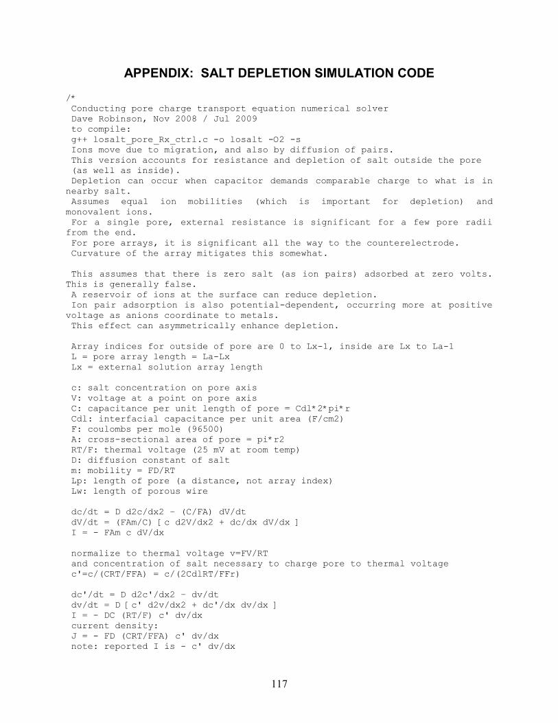
117
APPENDIX: SALT DEPLETION SIMULATION CODE /* Conducting pore charge transport equation numerical solver Dave Robinson, Nov 2008 / Jul 2009 to compile: g++ losalt_pore_Rx_ctrl.c -o losalt -O2 -s Ions move due to migration, and also by diffusion of pairs. This version accounts for resistance and depletion of salt outside the pore (as well as inside). Depletion can occur when capacitor demands comparable charge to what is in nearby salt. Assumes equal ion mobilities (which is important for depletion) and monovalent ions. For a single pore, external resistance is significant for a few pore radii from the end. For pore arrays, it is significant all the way to the counterelectrode. Curvature of the array mitigates this somewhat. This assumes that there is zero salt (as ion pairs) adsorbed at zero volts. This is generally false. A reservoir of ions at the surface can reduce depletion. Ion pair adsorption is also potential-dependent, occurring more at positive voltage as anions coordinate to metals. This effect can asymmetrically enhance depletion. Array indices for outside of pore are 0 to Lx-1, inside are Lx to La-1 L = pore array length = La-Lx Lx = external solution array length c: salt concentration on pore axis V: voltage at a point on pore axis C: capacitance per unit length of pore = Cdl*2*pi*r Cdl: interfacial capacitance per unit area (F/cm2) F: coulombs per mole (96500) A: cross-sectional area of pore = pi*r2 RT/F: thermal voltage (25 mV at room temp) D: diffusion constant of salt m: mobility = FD/RT Lp: length of pore (a distance, not array index) Lw: length of porous wire dc/dt = D d2c/dx2 – (C/FA) dV/dt dV/dt = (FAm/C) [c d2V/dx2 + dc/dx dV/dx ] I = - FAm c dV/dx normalize to thermal voltage v=FV/RT and concentration of salt necessary to charge pore to thermal voltage c'=c/(CRT/FFA) = c/(2CdlRT/FFr) dc'/dt = D d2c'/dx2 – dv/dt dv/dt = D [c' d2v/dx2 + dc'/dx dv/dx ] I = - DC (RT/F) c' dv/dx current density: J = - FD (CRT/FFA) c' dv/dx note: reported I is - c' dv/dx
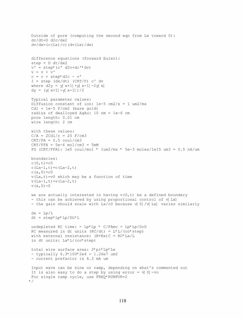
118
Outside of pore (computing the second eqn from Lx toward 0): dc/dt=D d2c/dx2 dv/dx=(c(Lx)/c)(dv(Lx)/dx) difference equations (forward Euler): step = D dt/dx2 v' = step*(c' d2v+dc'*dv) v = v + v' c = c + step*d2c - v' I = step (dx/dt) (CRT/F) c' dv where d2y = y[x+1]+y[x-1]-2y[x] dy = (y[x+1]-y[x-1])/2 Typical parameter values: Diffusion constant of ion: 1e-5 cm2/s = 1 um2/ms Cdl = 1e-5 F/cm2 (bare gold) radius of dealloyed AgAu: 10 nm = 1e-6 cm pore length: 0.01 cm wire length: 2 cm with these values: C/A = 2Cdl/r = 20 F/cm3 CRT/FA = 0.5 coul/cm3 CRT/FFA = 5e-6 mol/cm3 = 5mM FD (CRT/FFA): 1e5 coul/mol * 1um2/ms * 5e-3 moles/1e15 um3 = 0.5 nA/um boundaries: c(0,t)=c0 c(La-1,t)=c(La-2,t) c(x,0)=c0 v(Lx,t)=v0 which may be a function of time v(La-1,t)=v(La-2,t) v(x,0)=0 we are actually interested in having v(0,t) be a defined boundary - this can be achieved by using proportional control of v[Lx] - the gain should scale with Lx/c0 because v[0]/v[Lx] varies similarly dx = Lp/L dt = step*Lp*Lp/DL*L undepleted RC time: = Lp*Lp * C/FAmc = Lp*Lp/Dc0 RC measured in dt units (RC/dt) = L*L/(co*step) with external resistance: (R+Rx)C = RC*La/L in dt units: La*L/(co*step) total wire surface area: 2*pi*Lp*Lw - typically 6.3*100*2e4 = 1.26e7 um2 - current prefactor is 6.3 mA um Input wave can be sine or ramp, depending on what's commented out It is also easy to do a step by using error = v[0]-vo For single ramp cycle, use FREQ*RUNFOR=2 */

119
#include <iostream> #include <fstream> #include <cstring> #include <ctime> #include <cstdlib> #include <cmath> #define FILENAME "poreramp.txt" #define Lx 100 // array length of outside-pore section #define La 500 // total array length #define Lp 100.0 // pore length in micrometers #define co 3.0 // initial concentration in pore #define vo 10.0 // step to this voltage (normalized units for both of these) #define RUNFOR 0.25 // simulation time in units of ideal RC time #define FREQ 8 // frequency of input wave in units of ideal RC time // corner freq is 1/2pi = 0.159 #define PTSPERCYCLE 256 // data points recorded per cycle of input wave #define STEP 0.01 #define DELIM ((char)9) // tab #define DOANIM 0 // record animation data for use in animacro.xls using namespace std; main() long start_time=clock(); double xstep = Lp/(La-Lx); // length unit = micrometer double tstep = xstep*xstep*STEP; // time unit = ms with D=1um2/ms // this way, the factors step*xstep/tstep in the I definition = 1/xstep // a current of 1 will charge 1 micrometer of the pore to RT/F (25 mV) in 1 ms double RC = ((La-Lx)*La)/(co*STEP); // RC time in dt units double RCtime = RC*STEP*Lp*Lp/(1000*(La-Lx)*(La-Lx)); // RC time in seconds long tmax = (long)floor((double)RUNFOR*RC); long period = (long)ceil(RC/(double)FREQ); long tmod = (long)floor(period/(double)PTSPERCYCLE); if (tmod<=0) tmod=tmax; double error = 0.0; // for proportional control double vgain = 0.001; int xmod = (int)ceil(La/250); if (xmod<=0) xmod=La; // salt concentration and derivatives double c[La]; double dc[La]; double d2c[La]; // voltage and derivatives double v[La]; double dv[La]; double d2v[La];

120
double dva[La]; // current double i[La]; // time series for output double t0[(long)(RUNFOR*FREQ*PTSPERCYCLE)]; // this is equal to tmax/tmod double i0[(long)(RUNFOR*FREQ*PTSPERCYCLE)]; double c0[(long)(RUNFOR*FREQ*PTSPERCYCLE)]; double v0[(long)(RUNFOR*FREQ*PTSPERCYCLE)]; int x=0; long t=0; long ts=0; for (x=0;x<La;x++) c[x]=co; dc[x]=0.0; d2c[x]=0.0; v[x]=0.0; dv[x]=0.0; d2v[x]=0.0; dva[x]=0.0; i[x]=0.0; ofstream outfile(FILENAME); if (outfile) cout << "opened file" << endl; else cout << "failed to open file" << endl; outfile << "nanopore charging model DBR Jul 2009" << endl; outfile << "assumes diffusion constant is 1 um2/ms" << endl; outfile << "co" << DELIM << co << DELIM << "units = CRT/FFA; co=1 is enough salt to charge pore to thermal voltage" << endl; outfile << "vo" << DELIM << vo << DELIM << "units = RT/F" << endl; outfile << "Lx" << DELIM << Lx << DELIM << "array elements outside of pore" << endl; outfile << "La" << DELIM << La << DELIM << "total array elements" << endl; outfile << "tstep" << DELIM << tstep << DELIM << "ms" << endl; outfile << "xstep" << DELIM << xstep << DELIM << "micrometers" << endl; outfile << "RUNFOR" << DELIM << RUNFOR << endl; outfile << "FREQ" << DELIM << FREQ << endl; outfile << "STEP" << DELIM << STEP << endl; outfile << "vgain" << DELIM << vgain << endl; outfile << "RC" << DELIM << RCtime << DELIM << "RC time in sec" << endl; outfile << "Scanrate" << DELIM << 50*vo/(RCtime*RUNFOR) << DELIM << "mV/sec" << endl; if (DOANIM) outfile << "a" << DELIM << DELIM; for (x=0;x<La;x+=xmod) outfile << (x*xstep) << DELIM; outfile << endl; outfile << "e" << DELIM << DELIM; for (x=0;x<La;x+=xmod) outfile << (x*xstep) << DELIM; outfile << endl; outfile << "d" << endl;
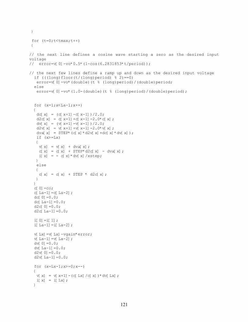
121
for (t=0;t<tmax;t++) // the next line defines a cosine wave starting a zero as the desired input voltage // error=v[0]-vo*0.5*(1-cos(6.2831853*t/period)); // the next few lines define a ramp up and down as the desired input voltage if (((long)floor(t/(long)period) % 2)==0) error=v[0]-vo*(double)(t % (long)period)/(double)period; else error=v[0]-vo*(1.0-(double)(t % (long)period)/(double)period); for (x=1;x<La-1;x++) dc[x] = (c[x+1]-c[x-1])/2.0; d2c[x] = c[x+1]+c[x-1]-2.0*c[x]; dv[x] = (v[x+1]-v[x-1])/2.0; d2v[x] = v[x+1]+v[x-1]-2.0*v[x]; dva[x] = STEP*(c[x]*d2v[x]+dc[x]*dv[x]); if (x>=Lx) v[x] = v[x] + dva[x]; c[x] = c[x] + STEP*d2c[x] - dva[x]; i[x] = - c[x]*dv[x]/xstep; else c[x] = c[x] + STEP * d2c[x]; c[0]=co; c[La-1]=c[La-2]; dc[0]=0.0; dc[La-1]=0.0; d2c[0]=0.0; d2c[La-1]=0.0; i[0]=i[1]; i[La-1]=i[La-2]; v[Lx]=v[Lx]-vgain*error; v[La-1]=v[La-2]; dv[0]=0.0; dv[La-1]=0.0; d2v[0]=0.0; d2v[La-1]=0.0; for (x=Lx-1;x>=0;x--) v[x] = v[x+1]-(c[Lx]/c[x])*dv[Lx]; i[x] = i[Lx];

122
if (t%(long)tmod==0 && ts<(long)(RUNFOR*FREQ*PTSPERCYCLE)) t0[ts]=tstep*(double)(t); v0[ts]=v[0]; c0[ts]=c[La-1]; i0[ts]= i[0]; if (DOANIM) outfile << "c" << DELIM << t0[ts] << DELIM; for (x=0;x<La;x+=xmod) outfile << c[x] << DELIM; outfile << endl; outfile << "v" << DELIM << t0[ts] << DELIM; for (x=0;x<La;x+=xmod) outfile << v[x] << DELIM; outfile << endl; ts++; cout << clock()-start_time << " ms to compute" << endl; outfile << endl << "time" << DELIM << "conc" << DELIM << "volts" << DELIM << "current" << endl; for (t=0; t<ts; t++) outfile << t0[t] << DELIM << c0[t] << DELIM << v0[t] << DELIM << i0[t] << endl; outfile.close(); return 0;
The following Microsoft Excel macro allows the animation output from the C++ program to be visualized: Sub animacrow() ' ' Animacrow ' 11/28/2008 by dbr ' Animate a graph by cycling adjacent Y rows. ' Make the graph first, with one row of X data ' Chart background should be white. ' Y data are below that, with one row per frame (255 max). ' Place cell at upper left of Y range and press ctrl-z. ' The chart should be closest to the upper left on the worksheet. ' This increments the column of displayed chart data and pauses, ' creating an animation of the data. ' This version is configured to work on worksheet 2. SheetNum = 2 ' Time units are apparently fractions of a day. ' The Wait function behaves strangely if the time is less than 1 second. ' However, the animation can go at a reasonable speed if so. OneSecond = 0.0000115741

123
' Get boundaries of data range row1 = Selection.Rows.Row row2 = Selection.End(xlDown).Rows.Row col1 = CStr(Selection.Columns.Column) col2 = CStr(Selection.End(xlToRight).Columns.Column) ' Activate first chart (move the chart to the upper left to make it first) Worksheets(SheetNum).ChartObjects(1).Activate ' Cycle through the columns For i = row1 To row2 j = CStr(i) ActiveChart.SeriesCollection(1).Values = "=Sheet" + CStr(SheetNum) + "!R" + j + "C" + col1 + ":R" + j + "C" + col2 Application.Wait (Now + 0.1 * OneSecond) Next ' Pause, then restore initial conditions Application.Wait (Now + 0.5 * OneSecond) ActiveChart.SeriesCollection(1).Values = "=Sheet" + CStr(SheetNum) + "!R" + CStr(row1) + "C" + col1 + ":R" + CStr(row1) + "C" + col Worksheets(SheetNum).Cells(row1, col1).Select End Sub

124
DISTRIBUTION (Electronic distribution upon release of report) External: Prof. Paul V. Braun Department of Materials Science and Engineering University of Illinois at Urbana-Champaign Prof. Roger J. Narayan Joint Department of Biomedical Engineering North Carolina State University and University of North Carolina Dr. Weon-Sik Chae Gangneung Center, Korea Basic Science Institute Internal: Ganesan Nagasubramanian 2546 David Ingersoll 2546 Thomas Wunsch 2546 Randy Cygan 6316 Justine Johannes 1810 Regan Stinnett 1821 Kevin Zavadil 1825 Susan Rempe 8653 Bruce Bunker 1816 Dale Huber 1132 Sean Hearne 1132 Erik Spoerke 1816 James Voigt 1816 Eric Ackerman 8653 Kevin Leung 1114 Todd Monson 1112 Art Pontau 8360 Roger Farrow 8353 Ray Ng 8248 Stewart Griffiths 8300 Bob Nilson 8365 Bill Even 8651 David B. Robinson 8651 Benjamin Jacobs 8651 Markus Ong 8651 Blake Simmons 8625 Glenn Kubiak 8600 Michael Bartsch 8125 Bob Crocker 8125

125
Rion Causey 8650 Central Technical Files 8944 Technical Library 4536 D. Chavez, LDRD Office 1011