Embed Size (px)
Citation preview
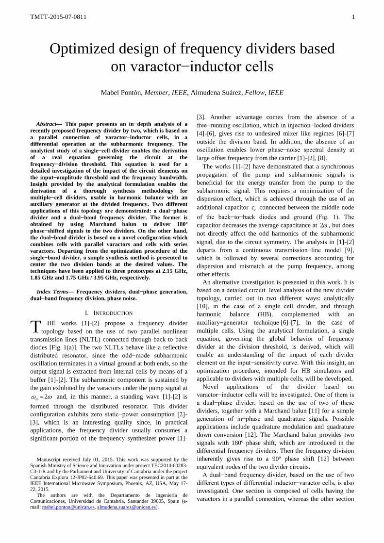
TMTT-2015-07-0811 1
Abstract— This paper presents an in−depth analysis of a
recently proposed frequency divider by two, which is based on a parallel connection of varactor−inductor cells, in a differential operation at the subharmonic frequency. The analytical study of a single−cell divider enables the derivation of a real equation governing the circuit at the frequency−division threshold. This equation is used for a detailed investigation of the impact of the circuit elements on the input−amplitude threshold and the frequency bandwidth. Insight provided by the analytical formulation enables the derivation of a thorough synthesis methodology for multiple−cell dividers, usable in harmonic balance with an auxiliary generator at the divided frequency. Two different applications of this topology are demonstrated: a dual−phase divider and a dual−band frequency divider. The former is obtained by using Marchand balun to deliver 180º phase−shifted signals to the two dividers. On the other hand, the dual−band divider is based on a novel configuration which combines cells with parallel varactors and cells with series varactors. Departing from the optimization procedure of the single−band divider, a simple synthesis method is presented to center the two division bands at the desired values. The techniques have been applied to three prototypes at 2.15 GHz, 1.85 GHz and 1.75 GHz / 3.95 GHz, respectively.
Index Terms— Frequency dividers, dual−phase generation,
dual−band frequency division, phase noise.
I. INTRODUCTION HE works [1]−[2] propose a frequency divider
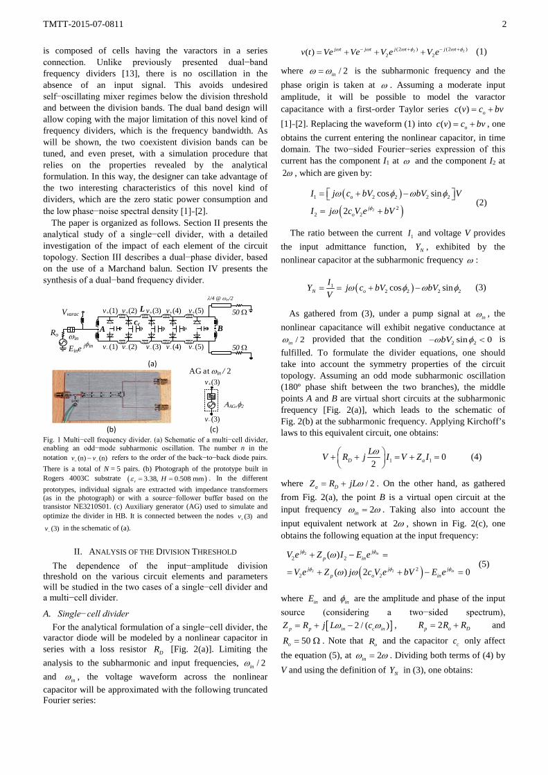
topology based on the use of two parallel nonlinear transmission lines (NLTL) connected through back to back diodes [Fig. 1(a)]. The two NLTLs behave like a reflective distributed resonator, since the odd−mode subharmonic oscillation terminates in a virtual ground at both ends, so the output signal is extracted from internal cells by means of a buffer [1]−[2]. The subharmonic component is sustained by the gain exhibited by the varactors under the pump signal at
2inω ω= and, in this manner, a standing wave [1]−[2] is formed through the distributed resonator. This divider configuration exhibits zero static−power consumption [2]− [3], which is an interesting quality since, in practical applications, the frequency divider usually consumes a significant portion of the frequency synthesizer power [1]−
Manuscript received July 01, 2015. This work was supported by the Spanish Ministry of Science and Innovation under project TEC2014-60283-C3-1-R and by the Parliament and University of Cantabria under the project Cantabria Explora 12-JP02-640.69. This paper was presented in part at the IEEE International Microwave Symposium, Phoenix, AZ, USA, May 17-22, 2015.
The authors are with the Departamento de Ingeniería de Comunicaciones, Universidad de Cantabria, Santander 39005, Spain (e-mail: [email protected], [email protected]).
[3]. Another advantage comes from the absence of a free−running oscillation, which in injection−locked dividers [4]−[6], gives rise to undesired mixer like regimes [6]−[7] outside the division band. In addition, the absence of an oscillation enables lower phase−noise spectral density at large offset frequency from the carrier [1]−[2], [8].
The works [1]−[2] have demonstrated that a synchronous propagation of the pump and subharmonic signals is beneficial for the energy transfer from the pump to the subharmonic signal. This requires a minimization of the dispersion effect, which is achieved through the use of an additional capacitor cc connected between the middle node of the back−to−back diodes and ground (Fig. 1). The capacitor decreases the average capacitance at 2ω , but does not directly affect the odd harmonics of the subharmonic signal, due to the circuit symmetry. The analysis in [1]−[2] departs from a continuous transmission−line model [9], which is followed by several corrections accounting for dispersion and mismatch at the pump frequency, among other effects.
An alternative investigation is presented in this work. It is based on a detailed circuit−level analysis of the new divider topology, carried out in two different ways: analytically [10], in the case of a single−cell divider, and through harmonic balance (HB), complemented with an auxiliary−generator technique [6]−[7], in the case of multiple cells. Using the analytical formulation, a single equation, governing the global behavior of frequency divider at the division threshold, is derived, which will enable an understanding of the impact of each divider element on the input−sensitivity curve. With this insight, an optimization procedure, intended for HB simulators and applicable to dividers with multiple cells, will be developed.
Novel applications of the divider based on varactor−inductor cells will be investigated. One of them is a dual−phase divider, based on the use of two of these dividers, together with a Marchand balun [11] for a simple generation of in−phase and quadrature signals. Possible applications include quadrature modulation and quadrature down conversion [12]. The Marchand balun provides two signals with 180º phase shift, which are introduced in the differential frequency dividers. Then the frequency division inherently gives rise to a 90º phase shift [12] between equivalent nodes of the two divider circuits.
A dual−band frequency divider, based on the use of two different types of differential inductor−varactor cells, is also investigated. One section is composed of cells having the varactors in a parallel connection, whereas the other section
Optimized design of frequency dividers based on varactor−inductor cells
Mabel Pontón, Member, IEEE, Almudena Suárez, Fellow, IEEE
T
TMTT-2015-07-0811 2
is composed of cells having the varactors in a series connection. Unlike previously presented dual−band frequency dividers [13], there is no oscillation in the absence of an input signal. This avoids undesired self−oscillating mixer regimes below the division threshold and between the division bands. The dual band design will allow coping with the major limitation of this novel kind of frequency dividers, which is the frequency bandwidth. As will be shown, the two coexistent division bands can be tuned, and even preset, with a simulation procedure that relies on the properties revealed by the analytical formulation. In this way, the designer can take advantage of the two interesting characteristics of this novel kind of dividers, which are the zero static power consumption and the low phase−noise spectral density [1]−[2].
The paper is organized as follows. Section II presents the analytical study of a single−cell divider, with a detailed investigation of the impact of each element of the circuit topology. Section III describes a dual−phase divider, based on the use of a Marchand balun. Section IV presents the synthesis of a dual−band frequency divider.
BA
(b) (c)
Vvaraccc
Lv+(1)
Ro ωin
Eine jφin
50 Ω
50 Ω
λ/4 @ ωin/2
AG at ωin / 2
ΑAG,φ2
(a)
v+(2)
v−(1) v−(2) v−(3) v−(4) v−(5)
v+(3) v+(4) v+(5)
v−(3)
v+(3)
Fig. 1 Multi−cell frequency divider. (a) Schematic of a multi−cell divider, enabling an odd−mode subharmonic oscillation. The number n in the notation (n) (n)+ −−v v refers to the order of the back−to−back diode pairs. There is a total of N = 5 pairs. (b) Photograph of the prototype built in Rogers 4003C substrate ( )3.38, 0.508 mmr Hε = = . In the different prototypes, individual signals are extracted with impedance transformers (as in the photograph) or with a source−follower buffer based on the transistor NE3210S01. (c) Auxiliary generator (AG) used to simulate and optimize the divider in HB. It is connected between the nodes (3)+v and
(3)−v in the schematic of (a).
II. ANALYSIS OF THE DIVISION THRESHOLD The dependence of the input−amplitude division
threshold on the various circuit elements and parameters will be studied in the two cases of a single−cell divider and a multi−cell divider.
A. Single−cell divider For the analytical formulation of a single−cell divider, the
varactor diode will be modeled by a nonlinear capacitor in series with a loss resistor DR [Fig. 2(a)]. Limiting the analysis to the subharmonic and input frequencies, / 2inω and inω , the voltage waveform across the nonlinear capacitor will be approximated with the following truncated Fourier series:
2 2(2 ) (2 )2 2( ) j t j tj t j tv t Ve Ve V e V eω φ ω φω ω + − +−= + + + (1)
where / 2inω ω= is the subharmonic frequency and the phase origin is taken at ω . Assuming a moderate input amplitude, it will be possible to model the varactor capacitance with a first−order Taylor series ( ) oc v c bv= + [1]−[2]. Replacing the waveform (1) into ( ) oc v c bv= + , one obtains the current entering the nonlinear capacitor, in time domain. The two−sided Fourier−series expression of this current has the component I1 at ω and the component I2 at 2ω , which are given by:
( )
( )2
1 2 2 2 2
22 2
cos sin
2
o
jo
I j c bV bV V
I j c V e bVφ
ω φ ω φ
ω
= + −
= + (2)
The ratio between the current 1I and voltage V provides the input admittance function, NY , exhibited by the nonlinear capacitor at the subharmonic frequency ω :
( )12 2 2 2cos sin= = + −N o
IY j c bV bVV
ω φ ω φ (3)
As gathered from (3), under a pump signal at inω , the nonlinear capacitance will exhibit negative conductance at
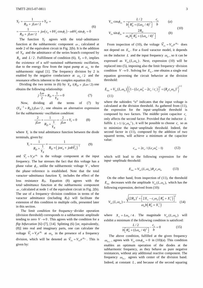
/ 2inω provided that the condition 2 2sin 0bVω φ− < is fulfilled. To formulate the divider equations, one should take into account the symmetry properties of the circuit topology. Assuming an odd mode subharmonic oscillation (180º phase shift between the two branches), the middle points A and B are virtual short circuits at the subharmonic frequency [Fig. 2(a)], which leads to the schematic of Fig. 2(b) at the subharmonic frequency. Applying Kirchoff’s laws to this equivalent circuit, one obtains:
1 1 02
+ + = + =
D aLV R j I V Z Iω (4)
where / 2ω= +a DZ R jL . On the other hand, as gathered from Fig. 2(a), the point B is a virtual open circuit at the input frequency 2ω ω=in . Taking also into account the input equivalent network at 2ω , shown in Fig. 2(c), one obtains the following equation at the input frequency:
( )
2
2 2
2 2
22 2
( )
( ) 2 0
φφ
φφ φ
ω
ω ω
+ − =
= + + − =
in
in
jjp in
jj jp o in
V e Z I E e
V e Z j c V e bV E e (5)
where inE and inφ are the amplitude and phase of the input source (considering a two−sided spectrum),
[ ]2 / ( )ω ω= + −p p in c inZ R j L c , 2= +p o DR R R and
50 oR = Ω . Note that oR and the capacitor cc only affect the equation (5), at 2inω ω= . Dividing both terms of (4) by V and using the definition of NY in (3), one obtains:
TMTT-2015-07-0811 3
( )2 2 2 2
1/ 2
1 cos sin 0/ 2
= + =+
= + + − =+
T ND
oD
Y YR jL
j c bV bVR jL
ω
ω φ ω φω
(6)
The function TY agrees with the total−admittance function at the subharmonic component ω , calculated at node 2 of the equivalent circuit in Fig. 2(b). It is the addition of NY and the admittance of the series branch composed by
DR and / 2L . Fulfillment of condition (6), 0=TY , implies the existence of a self−sustained subharmonic oscillation, due to the energy flow from the input pump at inω to the subharmonic signal [1]. The frequency division by 2 is enabled by the negative conductance at / 2inω and the resonance effects inherent to the complex equation (6).
Dividing the two terms in (6) by /( / 2)+N DY R jLω one obtains the following relationship:
1 02
+ + =DN
Lj RY
ω (7)
Now, dividing all the terms of (7) by 1( ) / 2− +N DY R jLω , one obtains an alternative expression
for the subharmonic−oscillation condition:
12 1 2 01+ = + =
+DN
YjL jLR
Yω ω
(8)
where 1Y is the total admittance function between the diode terminals, given by:
( )1 12
1 11 −= =
+ ++ D oDN
YR j c j bVR
Yω ω
(9)
and 22 2
jV V e φ= is the voltage component at the input frequency. The bar stresses the fact that this voltage has a phase value 2φ , unlike the subharmonic voltage V , where the phase−reference is established. Note that the total varactor−admittance function 1Y includes the effect of the loss resistance RD. Equation (8) agrees with the total−admittance function at the subharmonic component ω , calculated at node 1 of the equivalent circuit in Fig. 2(b). The use of a frequency−division condition in terms of the varactor admittance (including RD) will facilitate the extension of this condition to multiple cells, presented later in this section.
The limit condition for frequency−divider operation (division threshold) corresponds to a subharmonic amplitude tending to zero 0V → . This agrees with the condition for a flip bifurcation [6]−[7], [14]. Splitting (6) [or, equivalently, (8)] into real and imaginary parts, one can calculate the voltage 2
2 2φ= jV V e at ωin in the presence of a frequency
division, which will be denoted as 22 2
φ= ojo oV V e . This is
given by:
2 2 2 2
2 2 2 2
/ 2cos ( )( / 4)
2sin ( )
( / 4)
oo o
D in
Do o
in D in
cLV abb R L
RV bb R L
φω
φω ω
= − +
= +
(10)
From inspection of (10), the voltage 22 2
ojo oV V e φ= does
not depend on inE . For a fixed varactor model, it depends on the inductor L and the input frequency inω , so it can be expressed as 2 ( , )o inV L ω . Next, expression (10) will be replaced into (5), imposing also the limit frequency−division condition 0V → . Solving for inE , one obtains a single real equation governing the circuit behavior at the division threshold:
1/222 22 ( , ) 1 ( 2 / ) ( )ω ω ω = − − + ino o in o in o c p o inE V L Lc c c R c
(11)
where the subindex “o” indicates that the input voltage is calculated at the division threshold. As gathered from (11), the expression for the input−amplitude threshold is composed by two factors. The middle−point capacitor cc only affects the second factor. Provided that the inductor L fulfils 21/ ( )o inL c ω> , it will be possible to choose cc so as to minimize the input−amplitude threshold. Indeed, the second factor in (11), composed by the addition of two squared terms, will achieve a minimum at the capacitor value:
22 / ( 1)cm o o inc c Lc ω= − (12)
which will lead to the following expression for the input−amplitude threshold:
2 ( , )ω ω=ino o in p o inE V L R c (13)
On the other hand, from inspection of (11), the threshold inoE decreases with the amplitude 2 ( , ),o inV L ω which has the
following expression, derived from (10):
( )
( )
22 2 2
2 2 2
(2 ) 2( , )
D L o in D L
o inin D L
R X c R XV L
b R X
ωω
ω
+ − + =+
(14)
where / 4L inX Lω= . The magnitude 2 ( , )o inV L ω will exhibit a minimum if the following condition is satisficed:
2 2
/ 2 0( / 4)
o
D in
cLbb R Lω
− = +
(15)
The above condition, fulfilled at the given frequency ,in cω , agrees with 2 2cos 0o oV φ = in (10)(a). This condition
enables an optimum operation of the diodes at the subharmonic frequency, as they behave as pure negative resistances, without any additional reactive component. The frequency ,in cω agrees with center of the division band. Indeed, at constant L , and because of the second squaring
TMTT-2015-07-0811 4
operation under the root in (14), the frequency response will be nearly symmetrical about ,in cω .
RD2Rocc / 2
+
-V2
LRD
+
-V=V1
L/ 2
I1
RD
ωin
Ro
L
c(v)= co+bv
cc
+
-v(t)
L
Einejφin
BA
ωin
Einejφin
(a)
(b) (c)
1 2
Za
I2
Zp
( )21 2
φω= + joI j c bV e ( )2 2
2 22 φω= +joI j c V e bV
Fig. 2 Single−cell frequency divider. (a) Full topology. (b) Equivalent circuit at the subharmonic frequency ω . (c) Equivalent circuit at the input frequency 2inω ω= .
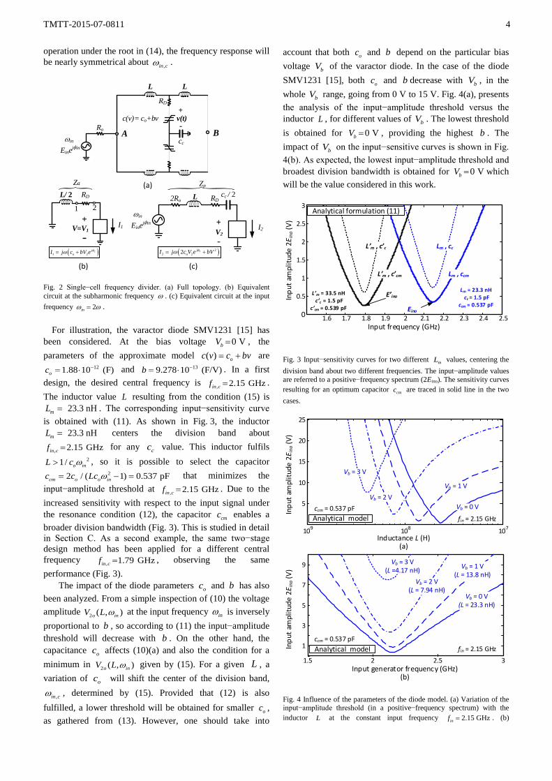
For illustration, the varactor diode SMV1231 [15] has
been considered. At the bias voltage 0 VbV = , the parameters of the approximate model ( ) oc v c bv= + are
121.88 10 (F)oc −= ⋅ and 139.278 10 (F/V)b −= ⋅ . In a first design, the desired central frequency is , 2.15 GHzin cf = . The inductor value L resulting from the condition (15) is
23.3 nHmL = . The corresponding input−sensitivity curve is obtained with (11). As shown in Fig. 3, the inductor
23.3 nHmL = centers the division band about
, 2.15 GHzin cf = for any cc value. This inductor fulfils 21/ o inL c ω> , so it is possible to select the capacitor
22 / ( 1) 0.537 pFcm o o inc c Lc ω= − = that minimizes the input−amplitude threshold at , 2.15 GHzin cf = . Due to the increased sensitivity with respect to the input signal under the resonance condition (12), the capacitor cmc enables a broader division bandwidth (Fig. 3). This is studied in detail in Section C. As a second example, the same two−stage design method has been applied for a different central frequency , 1 .79 GHzin cf = , observing the same performance (Fig. 3).
The impact of the diode parameters oc and b has also been analyzed. From a simple inspection of (10) the voltage amplitude 2 ( , )o inV L ω at the input frequency inω is inversely proportional to b , so according to (11) the input−amplitude threshold will decrease with b . On the other hand, the capacitance oc affects (10)(a) and also the condition for a minimum in 2 ( , )o inV L ω given by (15). For a given L , a variation of oc will shift the center of the division band,
,in cω , determined by (15). Provided that (12) is also fulfilled, a lower threshold will be obtained for smaller oc , as gathered from (13). However, one should take into
account that both oc and b depend on the particular bias voltage bV of the varactor diode. In the case of the diode SMV1231 [15], both oc and b decrease with bV , in the whole bV range, going from 0 V to 15 V. Fig. 4(a), presents the analysis of the input−amplitude threshold versus the inductor L , for different values of bV . The lowest threshold is obtained for 0 VbV = , providing the highest b . The impact of bV on the input−sensitive curves is shown in Fig. 4(b). As expected, the lowest input−amplitude threshold and broadest division bandwidth is obtained for 0 VbV = which will be the value considered in this work.
1.6 1.7 1.8 1.9 2 2.1 2.2 2.3 2.4 2.50
0.5
1
1.5
2
2.5
3
Input frequency (GHz)
Inpu
t am
plitu
de 2
E ino
(V)
Analytical formulation (11)
Eino
Lm , cc
Lm , ccm
L’m , c’c
L’m , c’cm
E’inoLm = 23.3 nH cc = 1.5 pF
ccm = 0.537 pF
L’m = 33.5 nH c’c = 1.5 pF
c’cm = 0.539 pF
Fig. 3 Input−sensitivity curves for two different mL values, centering the division band about two different frequencies. The input−amplitude values are referred to a positive−frequency spectrum (2Eino). The sensitivity curves resulting for an optimum capacitor cmc are traced in solid line in the two cases.
1.5 2 2.5 3
1
3
5
7
9
Vb = 0 V(L = 23.3 nH)
Vb = 1 V(L = 13.8 nH)
Vb = 2 V(L = 7.94 nH)
Vb = 3 V(L =4.17 nH)
Input generator frequency (GHz)
Inpu
t am
plitu
de 2
E ino
(V)
Analytical modelccm = 0.537 pF
(b)
10-9 10-8 10-7
5
10
15
20
25
Inductance L (H)
Inpu
t am
plitu
de 2
E ino
(V)
(a)
Vb = 3 V
Vb = 2 VVb = 1 V
Vb = 0 V
Analytical model
fin = 2.15 GHz
fin = 2.15 GHzccm = 0.537 pF
Fig. 4 Influence of the parameters of the diode model. (a) Variation of the input−amplitude threshold (in a positive−frequency spectrum) with the inductor L at the constant input frequency 2.15 GHzinf = . (b)
TMTT-2015-07-0811 5
Input−sensitivity curve with the bias voltage bV , choosing, in each case, the inductor value that provides the minimum input−amplitude threshold at
2.15 GHzinf = .
B. Multi−cell divider A multi−cell divider, such as the one considered in Fig. 1(a), will be investigated. Initially, the study will be carried out using the model ( ) oc v c bv= + at the two frequencies / 2inω and inω . The frequency−division condition (8) can be generalized to a multi−cell divider, which is done by means of an equivalent circuit analogous to the one in Fig. 2(b). The circuit total admittance is calculated at the node located between the first inductor and the rest of the varactor−inductor structure, at the subharmonic frequency ω . This provides the following recursive equation:
1
11
1
11(2)1 1(1) 0
1(3)...
ω
ωω
ω
− +
+ + + = +
+ +
jLY
Y jLjLY
jL
(16) where 1( )Y n , with 1 to n N= , are the diode subharmonic admittance functions and N is the number of back−to−back varactor pairs existing in the multi−cell divider, indexed as shown in Fig. 1(a). The admittance functions 1( )Y n are defined as:
( )
1 12
1( )( )D o
Y nR j c j bV nω ω
−=
+ + (17)
Note that for 1 N = , one has 1 1(1)Y Y≡ [see (7)−(9)]. In the above expression 2 ( )V n is the voltage component at inω across the nonlinear capacitor n . The bar stresses the fact that it is a complex magnitude. Equation (16) agrees with the flip bifurcation condition of the multi−cell divider. Combining (17) with (16), one obtains a complex equation of the form: 2 2 2( (1), , ( ), , ( ), , , , ) 0T oY V V n V N c b L ω =
(18)
which depends on the whole set of second harmonic voltages 2 ( )V n at inω , calculated under the limit condition for frequency division 0V → . These voltages provide the negative resistances that should compensate the passive impedances exhibited by the circuit at / 2inω , depending only on oc , b and L . Using the first−order capacitance model and the two analysis frequencies / 2inω and inω under the condition 0V → , the phasors 2 ( )V n will depend
linearly on the input voltage injinE e φ , since the diode
capacitance at inω is simply oc . A different expression will exist for each phasor, having the general form:
2 ( ) ( , , , 2 ) injn c o inV n A c c L E e φω= (19)
The replacement of (19) in (16) provides a complex nonlinear equation in inE and inφ , which can only be accurately resolved in a numerical manner. Because the flip−bifurcation (18) does not explicitly depend on cc , one may expect a behaviour analogous to that of a single cell, regarding the two design parameters L and cc . That is, the variation of L will shift the division band and the variation of cc will modify the sensitivity to the input signal and, therefore, the division threshold. However, as gathered from (16), the optimum values of L and cc for a desired central frequency ,in cω will depend on the number of cells and should be optimized for each N . Note that when implementing a multi−cell configuration, divisions by higher order will not be usually observed, due to the loading effects of the L−varactor cells, which are tuned for frequency division by 2, instead of higher order divisions
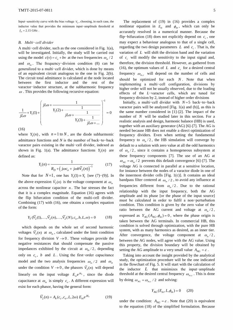
Initially, a multi−cell divider with 5=N back−to−back varactor pairs will be analyzed [Fig. 1(a) and (b)], as this is the same number considered in [1]−[2]. The impact of the number of N will be studied later in this section. For a realistic analysis and design, harmonic balance (HB) is used, together with an auxiliary generator (AG) [6]−[7]. The AG is needed because HB does not enable a direct optimization of frequency dividers. Even when setting the fundamental frequency to / 2inω , the HB simulation will converge by default to a solution with zero value at all the odd harmonics of / 2inω , since it contains a homogeneous subsystem at these frequency components [7]. The use of an AG at
/ 2AG inω ω= prevents this default convergence [6]−[7]. The voltage AG is connected in parallel at a sensitive location, for instance between the nodes of a varactor diode in one of the innermost divider cells [Fig. 1(c)]. It contains an ideal bandpass filter centered at / 2inω , to avoid any influence at frequencies different from / 2inω . Due to the rational relationship with the input frequency, both the AG amplitude and its phase [or the phase of the input source] must be calculated in order to fulfil a non−perturbation condition. This condition is given by the zero value of the ratio between the AG current and voltage at / 2inω , expressed as ( , ) 0AG AG inY A φ = , where the phase origin is taken between the AG terminals. In commercial HB, this condition is solved through optimization, with the pure HB system, with as many harmonics as desired, as an inner tier. After convergence, the voltage component at / 2inω , between the AG nodes, will agree with the AG value. Using this property, the division boundary will be obtained by setting the AG amplitude to a very small value AGA ε= .
Taking into account the insight provided by the analytical study, the optimization procedure will be the one indicated in the flowchart of Fig. 5. It will start with the calculation of the inductor L that minimizes the input−amplitude threshold at the desired central frequency ,in cω . This is done by doing , / 2AG in cω ω= and solving:
( , , ) 0AG in inY E L φ = (20)
under the condition: AGA ε= . Note that (20) is equivalent to the equation (18) of the simplified formulation. Because
TMTT-2015-07-0811 6
equation (20) is complex, it contains two real equations in three unknowns, which provides a curve in the plane defined by L and inE . To center the division band, L is swept, solving the complex equation (20) in terms of ,in inE φ at each L step. The L value providing the minimum inE is chosen. For illustration, the method will be applied to the divider shown in Fig. 1(a). In all the HB analyses presented hereafter, full diode models (including parasitics) and
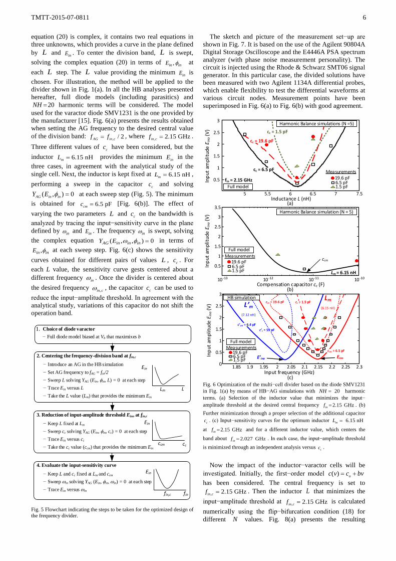
20NH = harmonic terms will be considered. The model used for the varactor diode SMV1231 is the one provided by the manufacturer [15]. Fig. 6(a) presents the results obtained when setting the AG frequency to the desired central value of the division band: , / 2AG in cf f= , where , 2.15 GHzin cf = . Three different values of cc have been considered, but the inductor 6.15 nHmL = provides the minimum inE in the three cases, in agreement with the analytical study of the single cell. Next, the inductor is kept fixed at 6.15 nHmL = , performing a sweep in the capacitor cc and solving
( , ) 0AG in inY E φ = at each sweep step (Fig. 5). The minimum is obtained for 6.5 pFcmc = [Fig. 6(b)]. The effect of varying the two parameters L and cc on the bandwidth is analyzed by tracing the input−sensitivity curve in the plane defined by inω and inE . The frequency inω is swept, solving the complex equation ( , , ) 0AG in in inY E ω φ = in terms of
,in inE φ at each sweep step. Fig. 6(c) shows the sensitivity curves obtained for different pairs of values L , cc . For each L value, the sensitivity curve gests centered about a different frequency inω . Once the divider is centered about the desired frequency ,in cω , the capacitor cc can be used to reduce the input−amplitude threshold. In agreement with the analytical study, variations of this capacitor do not shift the operation band.
1. Choice of diode varactor − Full diode model biased at Vb that maximixes b
2. Centering the frequency-division band at fin,c
Ein
L Lm
− Introduce an AG in the HB simulation− Set AG frequency to fAG = fin/2 − Sweep L solving YAG (Ein, φin, L) = 0 at each step − Trace Ein versus L− Take the L value (Lm) that provides the minimum Ein
3. Reduction of input-amplitude threshold Eino at fin,c
− Keep L fixed at Lm
− Sweep cc solving YAG (Ein, φin, cc) = 0 at each step − Trace Ein versus cc
− Take the cc value (ccm) that provides the minimum Ein
Ein
cc ccm
4. Evaluate the input-sensitivity curve
− Keep L and cc fixed at Lm and ccm
− Sweep ωin solving YAG (Ein, φin, ωin) = 0 at each step − Trace Ein versus ωin
Ein
fin fin,c Fig. 5 Flowchart indicating the steps to be taken for the optimized design of the frequency divider.
The sketch and picture of the measurement set−up are shown in Fig. 7. It is based on the use of the Agilent 90804A Digital Storage Oscilloscope and the E4446A PSA spectrum analyzer (with phase noise measurement personality). The circuit is injected using the Rhode & Schwarz SMT06 signal generator. In this particular case, the divided solutions have been measured with two Agilent 1134A differential probes, which enable flexibility to test the differential waveforms at various circuit nodes. Measurement points have been superimposed in Fig. 6(a) to Fig. 6(b) with good agreement.
fin = 2.15 GHz
cc = 6.5 pF
cc = 19.6 pF
Inductance L (nH)(a)
Inpu
t am
plitu
de E
ino (
V) cc = 1.5 pF
5 5.5 6 6.5 7 7.5
Harmonic Balance simulations (N =5)
0.5
1
1.5
2
2.5
3
10-13 10-12 10-11 10-10
0.5
1
1.5
2
2.5
3
3.5In
put a
mpl
itude
Ein
o (V)
Compensation capacitor cc (F)
ccm
Harmonic Balance simulation (N = 5)
Lm = 6.15 nH
(b)
6.5 pF19.6 pF
1.5 pF
6.5 pF19.6 pF
1.5 pF
Measurements
Measurements
1.85 1.9 1.95 2 2.05 2.1 2.15 2.2 2.25 2.30
0.5
1
1.5
2
2.5
3
Input frequency (GHz)
Inpu
t am
plitu
de E
ino (
V)
HB simulation
EinoE’ino
ccm = 6.5 pF
ccx = 19.6 pFL’m
(7.12 nH)
cc = 1.5 pF
6.5 pF19.6 pF1.5 pF
Measurements
(c)
c’c = 59 pFc’cm = 6.4 pF
Lm
(6.15 nH)
Full model
Full model
Full model
Fig. 6 Optimization of the multi−cell divider based on the diode SMV1231 in Fig. 1(a) by means of HB−AG simulations with 20NH = harmonic terms. (a) Selection of the inductor value that minimizes the input−
amplitude threshold at the desired central frequency 2.15 GHzinf = . (b) Further minimization through a proper selection of the additional capacitor
cc . (c) Input−sensitivity curves for the optimum inductor 6.15 nHmL =
at 2.15 GHzinf = and for a different inductor value, which centers the
band about 2.027 GHzinf = . In each case, the input−amplitude threshold is minimized through an independent analysis versus cc .
Now the impact of the inductor−varactor cells will be
investigated. Initially, the first−order model ( ) oc v c bv= + has been considered. The central frequency is set to
, 2.15 GHzin cf = . Then the inductor L that minimizes the input−amplitude threshold at , 2.15 GHzin cf = is calculated numerically using the flip−bifurcation condition (18) for different N values. Fig. 8(a) presents the resulting
TMTT-2015-07-0811 7
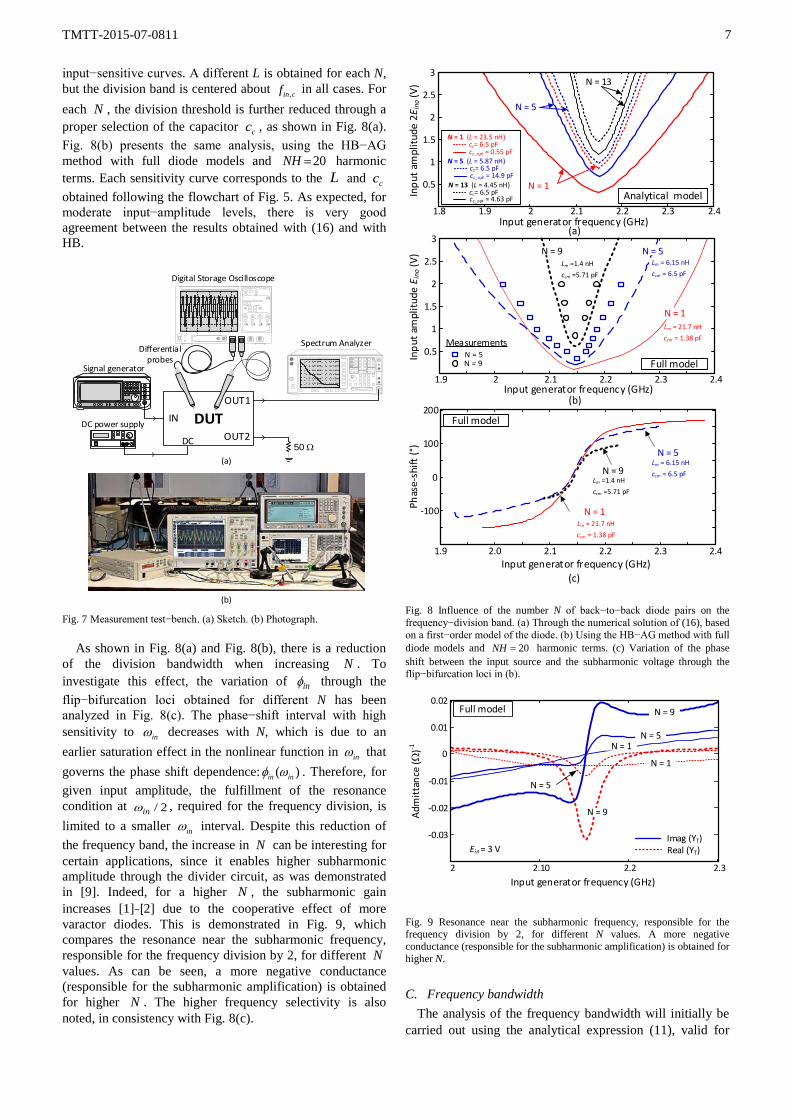
input−sensitive curves. A different L is obtained for each N, but the division band is centered about ,in cf in all cases. For each N , the division threshold is further reduced through a proper selection of the capacitor cc , as shown in Fig. 8(a). Fig. 8(b) presents the same analysis, using the HB−AG method with full diode models and 20NH = harmonic terms. Each sensitivity curve corresponds to the L and cc obtained following the flowchart of Fig. 5. As expected, for moderate input−amplitude levels, there is very good agreement between the results obtained with (16) and with HB.
(a)
(b)
DUTOUT1
OUT2
Digital Storage Oscilloscope
Spectrum Analyzer
50 Ω
IN
DC
Signal generator
DC power supply
Differential probes
Fig. 7 Measurement test−bench. (a) Sketch. (b) Photograph. As shown in Fig. 8(a) and Fig. 8(b), there is a reduction
of the division bandwidth when increasing N . To investigate this effect, the variation of inφ through the flip−bifurcation loci obtained for different N has been analyzed in Fig. 8(c). The phase−shift interval with high sensitivity to inω decreases with N, which is due to an earlier saturation effect in the nonlinear function in inω that governs the phase shift dependence: ( )in inφ ω . Therefore, for given input amplitude, the fulfillment of the resonance condition at / 2inω , required for the frequency division, is limited to a smaller inω interval. Despite this reduction of the frequency band, the increase in N can be interesting for certain applications, since it enables higher subharmonic amplitude through the divider circuit, as was demonstrated in [9]. Indeed, for a higher N , the subharmonic gain increases [1]−[2] due to the cooperative effect of more varactor diodes. This is demonstrated in Fig. 9, which compares the resonance near the subharmonic frequency, responsible for the frequency division by 2, for different N values. As can be seen, a more negative conductance (responsible for the subharmonic amplification) is obtained for higher N . The higher frequency selectivity is also noted, in consistency with Fig. 8(c).
1.9 2.0 2.1 2.2 2.3 2.4
-100
0
100
200
Input generator frequency (GHz)
1.9 2 2.1 2.2 2.3 2.4
0.5
1
1.5
2
2.5
3
Input generator frequency (GHz)
Full model
Inpu
t am
plitu
de E
ino (
V)
N = 9 N = 5
Measurements
Lm = 21.7 nHccm = 1.38 pF
Lm = 6.15 nH ccm = 6.5 pF
Lm =1.4 nH ccm =5.71 pF
N = 1
(a)
(b)
Full model
N = 9Lm =1.4 nH ccm =5.71 pF
N = 5Lm = 6.15 nH ccm = 6.5 pF
Lm = 21.7 nHccm = 1.38 pF
N = 1
(c)
1.8 1.9 2 2.1 2.2 2.3 2.4
0.5
1
1.5
2
2.5
3
N = 1
N = 5
N = 13
Input generator frequency (GHz)
Inpu
t am
plitu
de 2
E ino
(V)
Analytical model
N = 1 (L = 23.5 nH)
cc_opt = 0.55 pFcc= 6.5 pF
N = 5 (L = 5.87 nH)
cc_opt = 14.9 pFcc= 6.5 pF
N = 13 (L = 4.45 nH)
cc_opt = 4.63 pFcc= 6.5 pF
N = 5N = 9
Fig. 8 Influence of the number N of back−to−back diode pairs on the frequency−division band. (a) Through the numerical solution of (16), based on a first−order model of the diode. (b) Using the HB−AG method with full diode models and 20NH = harmonic terms. (c) Variation of the phase shift between the input source and the subharmonic voltage through the flip−bifurcation loci in (b).
2 2.10 2.2 2.3
-0.03
-0.02
-0.01
0
0.01
0.02
Input generator frequency (GHz)
N = 9
Imag (YT)Real (YT)
Full model
Ein = 3 V
N = 5N = 1
N = 1
N = 9
N = 5
Fig. 9 Resonance near the subharmonic frequency, responsible for the frequency division by 2, for different N values. A more negative conductance (responsible for the subharmonic amplification) is obtained for higher N.
C. Frequency bandwidth The analysis of the frequency bandwidth will initially be
carried out using the analytical expression (11), valid for
TMTT-2015-07-0811 8
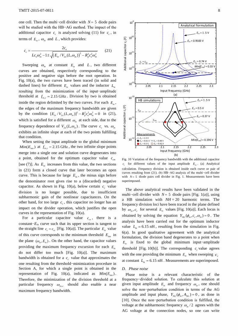
one cell. Then the multi−cell divider with 5=N diode pairs will be studied with the HB−AG method. The impact of the additional capacitor cc is analyzed solving (11) for cc , in terms of inE , inω and L , which provides:
( )22 2 2 22
2
1 / ( , )ω ω ω=
− ± −
oc
o in in o in p o in
cc
Lc E V L R c (21)
Sweeping inω at constant inE and L , two different curves are obtained, respectively corresponding to the positive and negative sign before the root operation. In Fig. 10(a), the two curves have been traced (in solid and dashed lines) for different inE values and the inductor mL resulting from the minimization of the input−amplitude threshold at , 2.15 GHzin cf = . Division by two is obtained inside the region delimited by the two curves. For each inE , the edges of the maximum frequency bandwidth are given by the condition 2 2 2 2
2[ / ( , )] 0ω ω− =in o in p o inE V L R c in (21), which is satisfied for a different inω at each side, due to the frequency dependence of 2 ( , )o inV L ω . The curve cc vs. inω exhibits an infinite slope at each of the two points fulfilling that condition.
When setting the input amplitude to the global minimum ( )inoMin E at , 2.15 GHzin cf = , the two infinite slope points
merge into a single one and solution curve degenerates into a point, obtained for the optimum capacitor value cmc [see (7)]. As inE increases from this value, the two sections in (21) form a closed curve that later becomes an open curve. This is because for large inE , the minus sign before the denominator root gives rise to a (discarded) negative capacitor. As shown in Fig. 10(a), below certain cc value division is no longer possible, due to insufficient subharmonic gain of the nonlinear capacitances. On the other hand, for too large cc , this capacitor no longer has an impact on the divider operation, which justifies the open curves in the representation of Fig. 10(a).
For a particular capacitor value cxc , there is a constant−Ein curve such that its upper section is tangent to the straight line c cxc c= [Fig. 10(a)]. The particular inE value of this curve corresponds to the minimum threshold inoE in the plane ( , )in inEω . On the other hand, the capacitor values providing the maximum frequency excursion for each inE do not differ too much [Fig. 10(a)]. The maximum bandwidth is obtained for a cc value that approximates the one resulting from the threshold−minimization procedure in Section A, for which a single point is obtained in the representation of Fig. 10(a), indicated as ( )inoMin E . Therefore, the minimization of the division threshold at a particular frequency ,in cω should also enable a near maximum frequency bandwidth.
2 2.05 2.1 2.15 2.2 2.25 2.3
10-12
10-11
10-10
Input frequency (GHz)
Addi
tiona
l cap
acito
r cc (
F)
Min(Eino) = 0.196 V
Ein = 0.37 V
Ein = 1 .5 V
Ein = 0.5 Vccx
ccm
HB simulations
MeasurementsEin = 1.5 V
Ein = 0.5 V Ein = 0.42 VEin = 0.48 VEin = 0.61 V
2 2.05 2.1 2.15 2.2 2.25 2.310-13
10-12
10-11
10-10
10-9
Input frequency (GHz)
Addi
tiona
l cap
acito
r cc (
F)
Min(Eino) = 0.33 V
Ein = 0.74 V
Ein = 1 .5 V
Analytical formulation
Ein = 0.9583 V
cc = ccx
ccm
(a)
(b) Fig. 10 Variation of the frequency bandwidth with the additional capacitor
cc for different values of the input amplitude inE . (a) Analytical calculation. Frequency division is obtained inside each curve or pair of curves resulting from (21). (b) HB−AG analysis of the multi−cell divider with 5=N diode pairs cell divider in Fig. 1. Measurements have been superimposed.
The above analytical results have been validated in the multi−cell divider with 5=N diode pairs [Fig. 1(a)], using a HB simulation with NH = 20 harmonic terms. The frequency division loci have been traced in the plane defined by ,in ccω for several inE values [Fig. 10(a)]. Each locus is obtained by solving the equation ( , , ) 0AG in c inY cφ ω = . The analysis have been carried out for the optimum inductor value 6.15 nHmL = , resulting from the simulation in Fig. 6(a). In good qualitative agreement with the analytical formulation, the division band degenerates to a point when
inE is fixed to the global minimum input−amplitude threshold [Fig. 10(b)]. The corresponding cc value agrees with the one providing the minimum inE when sweeping cc at constant 6.15 nHmL = . Measurements are superimposed.
D. Phase noise Phase noise is a relevant characteristic of the
frequency−divided solution. To calculate this solution at given input amplitude inE and frequency inω , one should solve the non−perturbation condition in terms of the AG amplitude and input phase, ( , ) 0AG in AGY Aφ = , as done in [10]. Once the non−perturbation condition is fulfilled, the voltage at the subharmonic frequency / 2inω agrees with the AG voltage at the connection nodes, so one can write
TMTT-2015-07-0811 9
1 AGV A= . For an understanding of the phase−noise behavior, the outer−tier function ( , )AG in AGY Aφ will be linearized about the divided steady−state solution in the presence of noise sources. The AG, which uses the pure HB system as an inner tier, enables control of the subharmonic voltage, so the partial derivatives with respect to V , inφ and ω , denoted as VY , Yφ and Yω , can be calculated through finite differences [8], [16]. The partial derivative
VY is obtained through increments in AGA , while keeping the frequency and phase constant at their original values,
, ino inoω φ , the ones fulfilling ( , ) 0AG AGo inoY A φ = . In turn, the partial derivative Yφ is obtained through increments in
inφ , while keeping the frequency and amplitude constant at their original values, ,ino AGoAω . An analogous procedure is carried out to calculate Yω .
In the phase−noise analysis, amplitude noise from the input source will be neglected, considering only the input phase noise ( )tψ . The phase noise of a divider by M is
expected to follow ( ) /t Mψ up to a certain offset frequency, usually beyond the region of influence of the circuit flicker noise. Thus, only white−noise sources will be considered. The circuit contains several white noise sources but they will all be modeled with a single equivalent current noise source. An example of the derivation of this kind of model is presented in [8]. The complex equivalent noise source, denoted as ( )NI t , is connected in parallel with the AG [8].
Taking into account the effect of the circuit noise sources, the total phase perturbation the observation node can be expressed as ( ) / 2 ( )T t tφ ψ φ∆ = + ∆ [8], [17]. In turn, the subharmonic amplitude undergoes an increment ( )V t∆ with respect to the steady−state value 1V . The time−varying phase and amplitude gives rise to an instantaneous complex frequency that can be expressed [8], [17]:
/ 21
( )2in
Vt jV
ψϕ ω φ ∆ = + + ∆ −
(22)
Then the phase−noise spectral density can be estimated with the following expression, derived in [7]−[8]:
( ) 2 22 2
V 22 1
2 2 2
24
( )
NV
T
V V
IY Y Y
V
Y Y Y Y
φ
φ ω
ψ
φ
Ω× +
∆ Ω =× + × Ω
(23)
where × indicates the cross product between real and imaginary parts. The varactor based divider will usually exhibit low frequency sensitivity, so it will be possible to approach the above equation with:
( ) 2
2 22 2 2
1
2( )4 sin ( )
T N
V
IY Vφ φ
ψφ
α α
Ω∆ Ω = +
− (24)
where φα is the angle of Yφ and Vα is the angle of VY . For low frequency sensitivity, the divider will follow the
divided phase noise of the input source up to certain offset frequency, from which the circuit white noise sources will dominate. This will give rise to a transition from a spectrum closely following that of the input source to a flat spectrum. The transition will occur at the offset frequency 0Ω for which the two terms in (24) have an identical magnitude. Assuming a low noise input source, the frequency 0Ω will
be larger for a higher magnitude Yφ , since this means a
higher sensitivity to the phase of the input source. It will also decrease with the subharmonic amplitude 1V and for angles Vφα α− close to an odd multiple of / 2π .
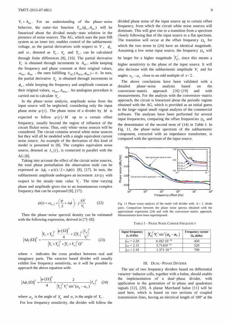
The above conclusions have been validated with a detailed phase−noise analysis based on the conversion−matrix approach [18]−[19] and with measurements. For the analysis with the conversion−matrix approach, the circuit is linearized about the periodic regime obtained with the AG, which is provided as an initial guess to the large−signal small−signal analysis of the commercial software. The analyses have been performed for several input frequencies, comparing the offset frequencies 0Ω and the denominator of the second term of (14) in Table I. In Fig. 11, the phase−noise spectrum of the subharmonic component, extracted with an impedance transformer, is compared with the spectrum of the input source.
103 104 105 106 107 108
-150
-130
-110
-90
-70
Input generator phase noise
Conversion matrix approach
Phas
e no
ise
(dBc
/Hz)
Frequency offset (Hz)
-150
-140
-130
10 5 10 7
Ω0 (fin1)Ω0 (fin2)Ω0 (fin3)
Fig. 11 Phase−noise analysis of the multi−cell divider with 5=N diode pairs. Comparison between the phase noise spectra obtained with the approximate expression (24) and with the conversion−matrix approach. Measurements have been superimposed.
TABLE I – PHASE NOISE CORNER FREQUENCY
Input frequency fin (GHz) ( )2 2 2
1 sin − VY Vφ φα α Frequency corner
Ω0 (kHz) fin1 = 2.20 4.182·10−10 450 fin2 = 2.15 5.71410−10 520 fin3 = 2.10 1.371·10−9 700
III. DUAL−PHASE DIVIDER The use of two frequency dividers based on differential
varactor−inductor cells, together with a balun, should enable the implementation of a dual−phase divider, with application in the generation of in−phase and quadrature signals [12], [20]. A planar Marchand balun [11] will be used here, which is based on two sections of coupled transmission lines, having an electrical length of 180º at the
TMTT-2015-07-0811 10
central operation frequency incω , as shown in Fig. 12. Initially, an analytical study of the configuration will be performed, using single−cell dividers [Fig. 12(a)]. Next, the practical case of a multi−cell divider with 5=N diode pairs will be studied [Fig. 12(b)−(c)], by means of numerical simulations and measurements.
In the simpler case of ideal transmission lines, the admittance matrix describing the Marchand balun at ,in cω is the following:
00 00 0
in in
a a
b b
I j j VI j VI j V
γ γγ
γ
− = −
(25)
where the currents and voltages at the three ports are defined as shown in Fig. 12(a). For generality, we will consider different voltage and current values at the inputs of the two dividers. This will be the case if one of the dividers is detuned with respect to the other. The analysis as a phase shifter requires full consideration of the nonlinear behavior with respect to the subharmonic components, so the components of the diode current will be given by (2), with
0V ≠ .
The matrix (25) provides the following relationships at the input frequency inω :
2
2
( ) ( )
' ( )
in a b
a in
b in
I j V j V aI j V I bI j V I c
γ γγ
γ
= − += − = −= = −
(26)
where the prima indicates variables referring to Divider B in Fig. 12. At the subharmonic frequency, each divider is terminated in virtual short circuits, so their individual subharmonic components fulfill:
1 1
1 1
0 ( )' ' 0 ( )
a
a
V Z I aV Z I b
+ =
+ = (27)
where aZ corresponds to the same impedance already defined in (4). Note that the phase origin is taken at the subharmonic component of the voltage across the varactor diode in the Divider A, so 1 'V is a phasor of the form:
11 1' ' jV V e φ= . Applying Kirchoff’s laws at the input
frequency inω , under consideration of (26)(b) and (26)(c), one obtains:
20
20
( )
' ( )
in in
in in
IE R I ajIE R I bj
γ
γ
− =
+ = (28)
Replacing alternatively (28)(a) and (28)(b) into (26)(a), the following equations are derived:
( )
( )
00 2 1 2 2 2
00 2 1 2 2 2
22 ( , ) '
2 '( ', ') '
in
in
GG E j Z I V V j V V
GG E j Z I V V j V V
γ γγ
γ γγ
= + + −
= − + + −
(29)
where 1/o oG R= and 2 ( )in c inZ jL j cω ω= − . The difference between the voltage and current values at the two diodes is due to their different bias voltages. In the approximate model (29) each divider is coupled to the other only at the input frequency inω .
(c)
(a)
Marchand Balun
Va
Vb
OCVinRo
Iin
Ia = - I2
Ib = - I´2Ein
RD
cc
+
-v(t)
LL
RD
cc
v(t)
LL+
-
Divider A
Divider B
B A
Eg,ωin,φg
Vvarac
cc
L
Rg
Marchand Balun
v’+(1)
B’A’
Vvarac2
cc
AG at ωin/2
ΑAG1, φAG1 = 0
λ/4 @ωin
Divider ADivider B
AG at ωin/2
ΑAG2, φAG2
(b)
0°
180°
90°
270°
v+(1)v+(2)v+(3)v+(4)v+(5)
v−(5) v−(4) v−(3) v−(2) v−(1)
v+(3)
v− (3)
v’+(3)
v’−(3)
v’+(2) v’+(3) v’+(4) v’+(5)
v’−(1) v’−(2) v’−(3) v’−(4) v’−(5)
Fig. 12 Dual−phase signal generator based on two varactor−based frequency dividers, connected through a Marchand balun. (a) Currents and voltages at the three ports of the Marchand balun. (b) Schematic. (c) Photograph of the prototype built in Rogers 4003C substrate ( )3.38, 0.508 mmr Hε = = .
To analyze the phase shifting capabilities, one should
determine the phase of the subharmonic voltage 11 1' ' jV V e φ=
since the phase of 1V is zero. The two nonlinear equations in (29) can only be resolved numerically, but they can provide an intuition on the impact of 2V on the phase shift. With this aim, the diode in Divider A is modeled with ,oc b . In turn the diode in Divider B, undergoing the biasing variations, is modeled with ', 'oc b . For a rough analysis of the impact of the coupling effects, one can define an equivalent current source:
0 2T
in inI G E j Vγ= + (30)
And solving (29)(b) for 2 'V one obtains:
2
12
0
' ''
'
TinI b V
Vc j
αβ γ
−=
+ (31)
where the following parameters with frequency dimension have been introduced 4 / 8oG Zα ω γ γω= + and
TMTT-2015-07-0811 11
2 / 4oG Zβ ω γ γω= + . Expression (31) will be replaced into (27)(b) considering the capacitance model ( ) ' 'oc v c b v= + to obtain the current component 1 'I . This leads to:
12 21
00
' '1 ' ' 0
'
jTin
aI e b V
j Z c bc j
φ αω
β γ
− −+ + = +
(32)
At a constant 2inω ω= , all the impedance terms will be constant too, so varying the parameters ', 'oc b will necessary give rise to a variation in 1 'V and 1φ . From (26)(b) and (26)(c), one has 2 2 'I I= − , so it is possible to obtain the following relationship:
2 22 1 2 12 2 ' ' ' 'o oc V bV c V b V+ = − − (33)
Because the biasing is varied in Divider B, one can expect the subharmonic amplitude to experience larger variations in this divider. Equation (33) indicates that the subharmonic oscillation may be extinguished in Divider B but not in the other, since, even when 1 ' 0V = , this equation can provide
1 0V ≠ . Of course, this condition will delimit the operation interval. For same bias voltage in the two dividers, one will have 0 0 'c c= and 'b b= , and due to the circuit symmetry, equation (33) will provide the solution:
901 1 2 2' , 'jV e V V V= = − (34)
Then, the two dividers are ruled by a same equation:
00 2 1 2 2
22 ( , ) 2in
GG E j Z I V V j Vγ γ
γ
= − + +
(35)
Due to the relationship (34), equivalent nodes of each divider will exhibit a 90° phase shift. This is indicated in Fig. 12(b). For instance, signals at the upper node of cell n in Divider B and at the upper node of the same cell n in divider A will exhibit a 90° phase shift. Signals at the lower node of cell n in Divider B and at the lower node of the same cell n in Divider A will also exhibit a 90° phase shift. On the other hand, upper and lower nodes of any cell in any of the two dividers will exhibit a 180° phase shift.
Fig. 13 presents the numerical analysis of a dual−phase signal generator based on the use of two one−cell dividers. It shows the variation of the subharmonic amplitudes in the two dividers when changing the bias voltage of Divider B. The analysis demonstrates the coupling between the two dividers since the amplitude in Divider A varies with this bias voltage. A practical dual−phase generator based on two multi−cell dividers with 5=N diode pairs has also been analyzed by means of two AGs, connected in a differential manner, at the central cell of each divider [Fig. 12(b)]. The amplitude variations are superimposed in Fig. 13 and exhibit the same qualitative behavior. In the two cases, the amplitude of Divider B undergoes the most significant variation, as this bias voltage directly affects the performance of the diodes in Divider B, whereas those in Divider A are affected by this bias voltage only through coupling effects. This gives rise to the amplitude imbalance observed in Fig. 13. With this hyperabrupt diode the
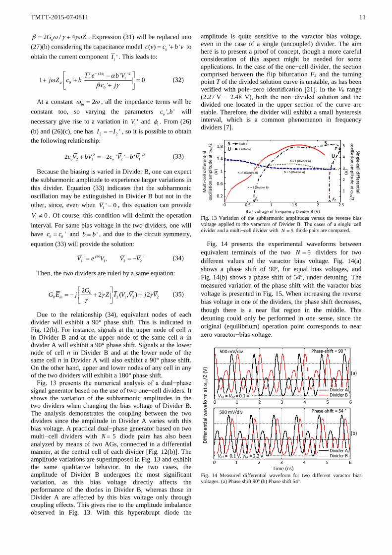
amplitude is quite sensitive to the varactor bias voltage, even in the case of a single (uncoupled) divider. The aim here is to present a proof of concept, though a more careful consideration of this aspect might be needed for some applications. In the case of the one−cell divider, the section comprised between the flip bifurcation F2 and the turning point T of the divided solution curve is unstable, as has been verified with pole−zero identification [21]. In the Vb range (2.27 V − 2.48 V), both the non−divided solution and the divided one located in the upper section of the curve are stable. Therefore, the divider will exhibit a small hysteresis interval, which is a common phenomenon in frequency dividers [7].
0.2
0.6
1
1.4
1.8
Mul
ti-ce
ll di
ffer
entia
l os
cilla
tion
ampl
itude
at ω
in/2
(V
)Bias voltage of frequency Divider B (V)
N = 5 (Divider A)
Single-cell differential oscillation am
plitude at ωin /2
(V)N =5 (Divider B)
N = 1 (Divider A)
1
2
3
4
5
0 0.5 1 1.5 2 2.5
N = 1 (Divider B)
T
F2F1
S
U
S U
Stable
Unstable
Fig. 13 Variation of the subharmonic amplitudes versus the reverse bias voltage applied to the varactors of Divider B. The cases of a single−cell divider and a multi−cell divider with 5=N diode pairs are compared.
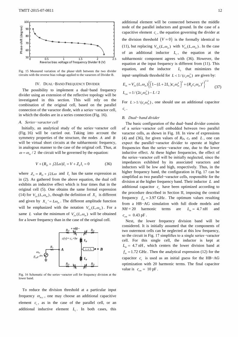
Fig. 14 presents the experimental waveforms between equivalent terminals of the two 5=N dividers for two different values of the varactor bias voltage. Fig. 14(a) shows a phase shift of 90º, for equal bias voltages, and Fig. 14(b) shows a phase shift of 54º, under detuning. The measured variation of the phase shift with the varactor bias voltage is presented in Fig. 15. When increasing the reverse bias voltage in one of the dividers, the phase shift decreases, though there is a near flat region in the middle. This detuning could only be performed in one sense, since the original (equilibrium) operation point corresponds to near zero varactor−bias voltage.
Time (ns)0 1 2 3 4 5 6
0 1 2 3 4 5 6
Diffe
rent
ial w
avef
orm
at ω
in/2
(V)
500 mV/div
Divider ADivider B
Divider ADivider B
(a)
(b)
500 mV/div
Phase-shift = 90 °
Phase-shift = 54 °
Vb1 = Vb2 = 0.1 V
Vb1 = 0.1 V, Vb2 = 2.2 V
Fig. 14 Measured differential waveform for two different varactor bias voltages. (a) Phase shift 90º (b) Phase shift 54º.
TMTT-2015-07-0811 12
0 0.5 1 1.5 2 2.550
60
70
80
100
90
Phas
e-sh
ift (d
egre
e)
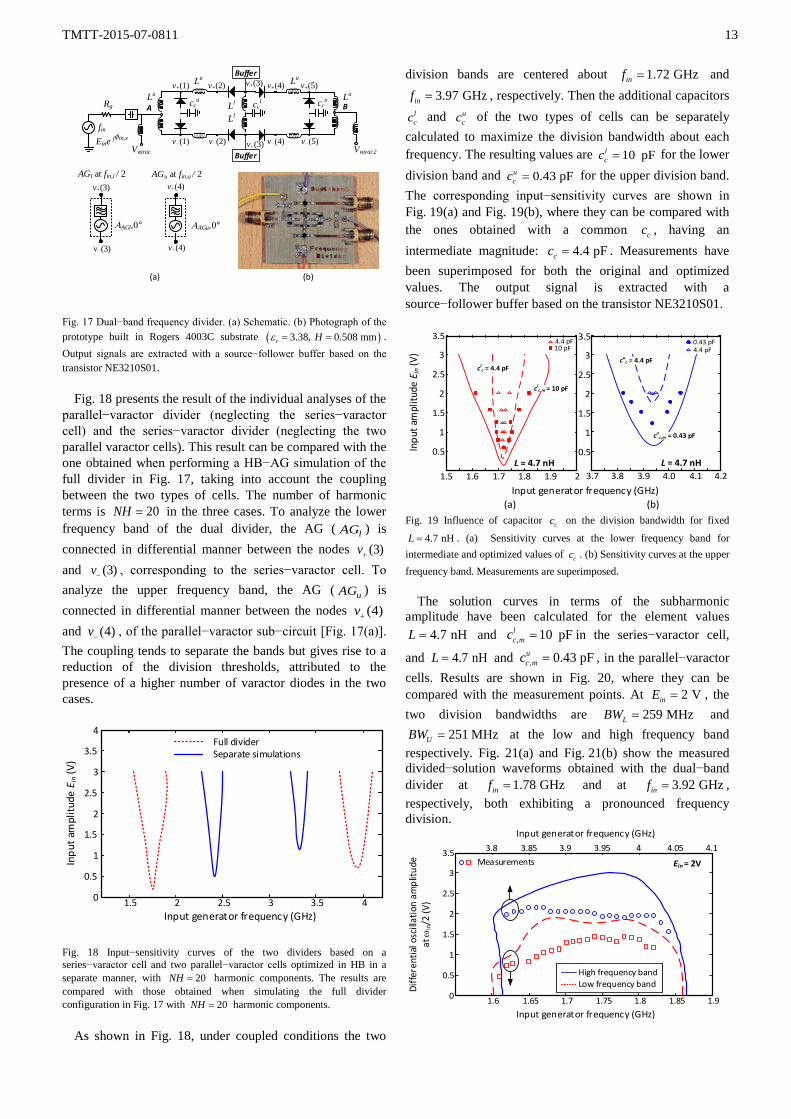
Reverse bias voltage of frequency Divider B (V) Fig. 15 Measured variation of the phase−shift between the two divider circuits with the reverse bias voltage applied to the varactors of Divider B.
IV. DUAL−BAND FREQUENCY DIVIDER The possibility to implement a dual−band frequency
divider using an extension of the reflective topology will be investigated in this section. This will rely on the combination of the original cell, based on the parallel connection of the varactor diode, with a series−varactor cell, in which the diodes are in a series connection (Fig. 16).
A. Series−varactor cell Initially, an analytical study of the series−varactor cell
(Fig. 16) will be carried out. Taking into account the symmetry properties of the structure, the nodes A and B will be virtual short circuits at the subharmonic frequency, in analogous manner to the case of the original cell. Thus, at
/ 2inω ω= the circuit will be governed by the equation: 1 1( 2 ) 0D bV R j L I V Z Iω+ + = + = (36)
where 2 ω= +b DZ R j L and 1I has the same expression as in (2). As gathered from the above equation, the dual cell exhibits an inductive effect which is four times that in the original cell (5). One obtains the same formal expression (14) for 2 ( , )o inV L ω , though the definition of LX is different and given by 'L inX Lω= . The different amplitude function will be emphasized with the notation '
2 ( , )o inV L ω . For a same L value the minimum of '
2 ( , )o inV L ω will be obtained for a lower frequency than in the case of the original cell.
ωin
Ro
Lp
c(v)= co+bv
+ -v(t)
Lp
Eine jφin
BA
RD RD
RD RD
cc or Lc
Fig. 16 Schematic of the series−varactor cell for frequency division at the lower band.
To reduce the division threshold at a particular input
frequency ,in cω , one may choose an additional capacitive
element cc , as in the case of the parallel cell, or an additional inductive element cL . In both cases, this
additional element will be connected between the middle node of the parallel inductors and ground. In the case of a capacitive element cc , the equation governing the divider at
the division threshold ( )0V = is the formally identical to
(11), but replacing 2 ( , )o inV L ω with '2 ( , )o inV L ω . In the case
of an additional inductor cL , the equation at the subharmonic component agrees with (36). However, the equation at the input frequency is different from (11). This equation, and the inductor cL that minimizes the input−amplitude threshold for 21/ ( )o inL c ω< are given by:
1/22' 2 22
2
( , ) 1 ( 2 ) ( )
1/ (2 ) / 2
ω ω ω
ω
= − + +
= −
in o in c o in p o in
cm o in
E V L L L c R c
L c L (37)
For 21/ ( )o inL c ω> , one should use an additional capacitor
cc .
B. Dual−band divider The basic configuration of the dual−band divider consists
of a series−varactor cell embedded between two parallel varactor cells, as shown in Fig. 18. In view of expressions (4) and (36), for given values of RD, co and L , one can expect the parallel−varactor divider to operate at higher frequencies than the series−varactor one, due to the lower inductive effect. At these higher frequencies, the effect of the series−varactor cell will be initially neglected, since the impedances exhibited by its associated varactors and inductors will be low and high, respectively. Thus, in the higher frequency band, the configuration in Fig. 17 can be simplified as two parallel−varactor cells, responsible for the division at the higher frequency band. Their inductor L and additional capacitor cc have been optimized according to the procedure described in Section II, imposing the central frequency 3.97 GHzinf = . The optimum values resulting from a HB−AG simulation with full diode models and NH = 20 harmonic terms are 4.7 nHmL = and
0.43 pFcmc = . Next, the lower frequency division band will be
considered. It is initially assumed that the components of two outermost cells can be neglected at this low frequency, so the circuit in Fig. 17 simplifies to a single series−varactor cell. For this single cell, the inductor is kept at
4.7 nHmL = , which centers the lower division band at 1.72 GHzinf = . Then the analytical expression (12) for the
capacitor cc is used as an initial guess for the HB−AG optimization with 20 harmonic terms. The final capacitor value is 10 pFcmc = .
TMTT-2015-07-0811 13
BA
Vvarac
ccu
Lu
Rg
AGu at fin,u / 2
Vvarac2
ccl cc
uLl
Ll
Lu
Lu
Lu
(a)
ΑAGu,0°
fin
Eine jφin,x
(b)
Buffer
Buffer
AGl at fin,l / 2
ΑAGl,0°
v+(1) v+(2) v+(3) v+(4) v+(5)
v−(5)v−(4)v−(3)v−(2)v−(1)
v+(3)
v−(3)
v+(4)
v−(4)
Fig. 17 Dual−band frequency divider. (a) Schematic. (b) Photograph of the prototype built in Rogers 4003C substrate ( )3.38, 0.508 mmr Hε = = . Output signals are extracted with a source−follower buffer based on the transistor NE3210S01.
Fig. 18 presents the result of the individual analyses of the
parallel−varactor divider (neglecting the series−varactor cell) and the series−varactor divider (neglecting the two parallel varactor cells). This result can be compared with the one obtained when performing a HB−AG simulation of the full divider in Fig. 17, taking into account the coupling between the two types of cells. The number of harmonic terms is 20NH = in the three cases. To analyze the lower frequency band of the dual divider, the AG ( lAG ) is connected in differential manner between the nodes (3)+v and (3)−v , corresponding to the series−varactor cell. To analyze the upper frequency band, the AG ( uAG ) is connected in differential manner between the nodes (4)+v and (4)−v , of the parallel−varactor sub−circuit [Fig. 17(a)]. The coupling tends to separate the bands but gives rise to a reduction of the division thresholds, attributed to the presence of a higher number of varactor diodes in the two cases.
Inpu
t am
plitu
de E
in (V
)
1.5 2 2.5 3 3.5 40
0.5
1
1.5
2
2.5
3
3.5
4
Input generator frequency (GHz)
Separate simulationsFull divider
Fig. 18 Input−sensitivity curves of the two dividers based on a series−varactor cell and two parallel−varactor cells optimized in HB in a separate manner, with 20NH = harmonic components. The results are compared with those obtained when simulating the full divider configuration in Fig. 17 with 20NH = harmonic components.
As shown in Fig. 18, under coupled conditions the two
division bands are centered about 1.72 GHzinf = and 3.97 GHzinf = , respectively. Then the additional capacitors
lcc and u
cc of the two types of cells can be separately calculated to maximize the division bandwidth about each frequency. The resulting values are 10 pFl
cc = for the lower division band and 0.43 pFu
cc = for the upper division band. The corresponding input−sensitivity curves are shown in Fig. 19(a) and Fig. 19(b), where they can be compared with the ones obtained with a common cc , having an intermediate magnitude: 4.4 pFcc = . Measurements have been superimposed for both the original and optimized values. The output signal is extracted with a source−follower buffer based on the transistor NE3210S01.
1.5 1.6 1.7 1.8 1.9 2
0.5
1
1.5
2
2.5
3
3.5
3.7 3.8 3.9 4.0 4.1 4.2
(a)
L = 4.7 nH
clc,m = 10 pF
clc = 4.4 pF
Input generator frequency (GHz)
Inpu
t am
plitu
de E
in (V
)
0.5
1
1.5
2
2.5
3
3.5
(b)
L = 4.7 nH
cuc,m = 0.43 pF
cuc = 4.4 pF
4.4 pF10 pF
0.43 pF4.4 pF
Fig. 19 Influence of capacitor cc on the division bandwidth for fixed
4.7 nHL = . (a) Sensitivity curves at the lower frequency band for intermediate and optimized values of cc . (b) Sensitivity curves at the upper frequency band. Measurements are superimposed.
The solution curves in terms of the subharmonic amplitude have been calculated for the element values
4.7 nHL = and , 10 pFlc mc = in the series−varactor cell,
and 4.7 nHL = and , 0.43 pFuc mc = , in the parallel−varactor
cells. Results are shown in Fig. 20, where they can be compared with the measurement points. At 2 VinE = , the two division bandwidths are 259 MHzLBW = and
251 MHzUBW = at the low and high frequency band respectively. Fig. 21(a) and Fig. 21(b) show the measured divided−solution waveforms obtained with the dual−band divider at 1.78 GHzinf = and at 3.92 GHzinf = , respectively, both exhibiting a pronounced frequency division.
Input generator frequency (GHz)
High frequency bandLow frequency band
1.6 1.65 1.7 1.75 1.8 1.85 1.90
0.5
1
1.5
2
2.5
3
3.5 3.8 3.85 3.9 3.95 4 4.05 4.1Input generator frequency (GHz)
Diffe
rent
ial o
scill
atio
n am
plitu
de
at ω
in/2
(V)
Ein = 2VMeasurements
TMTT-2015-07-0811 14
Fig. 20 Variation of the subharmonic amplitude versus the input frequency in each of the two division bands, obtained for constant 2 VinE = . Measurements have been superimposed.
0 1 2 3 4 5 6 7 8
200 mV/div
Time (nsec)0 1 2 3 4
Time (nsec)(a) (b)
200 mV/div
Fig. 21 Measured divided−solution waveforms obtained with the dual−band divider. (a) 1.78 GHzinf = . (b) 3.92 GHzinf = .
Finally, the phase−noise spectrum at each of the two
coexistent frequency−division bands, with respective input frequencies 1.78 GHzinf = and 3.92 GHzinf = , has been calculated and compared with the spectrum of the input source at each of the two frequencies. The results are shown in Fig. 22. The measured spectra are superimposed with good agreement. The respective corner frequencies 0Ω are different, which can be attributed to differences in the three
main magnitudes affecting the corner: Yφ , 1V and Vφα α− .
-140
-120
-100
-80
-140
-120
-100
-80
Phas
e no
ise
(dBc
/Hz)
Input generator phase noise
103 104 105 106 107 108
Frequency offset (Hz)
103 104 105 106 107 108
Input generator phase noise Upper division band
Lower division band
Conversion matrix approach
Conversion matrix approach
Fig. 22 Phase−noise spectrum at the central frequencies of the two coexistent division bands. Each spectrum is compared with that of the input source. Measurements are superimposed in the two cases. (a) 1.78 GHzinf = , in the lower division band. (b) 3.92 GHzinf = , in the
higher division band.
C. Pre−setting of the two division bands The possibility to center the two division bands at
specified frequency inlf and inuf has been investigated. Due to the coupling effect, one cannot center one band without affecting the other. This is shown in the analysis of Fig. 23, with measurement superimposed. Variations in lL ( uL ) enable a large shift of the lower (upper) division band, with a smaller undesired shift in the upper (lower) band. To circumvent this problem, an optimization procedure has been developed, based on the simultaneous optimization of two identical copies of the circuit, with identical element values lL , lc , uL and uc (Fig. 24). The first circuit copy operates at the desired central frequency of the lower division band, inlf , and is analyzed with an AG ( lAG ) at
/ 2AGl inlf f= , with an input−source phase ,in lφ . This AG is connected between the nodes of the series−varactor cell [Fig. 24(a)]. The second circuit copy operates at the desired central frequency of the upper division band, inuf , and is analyzed with an AG ( uAG ) at / 2=AGu inuf f , with an input−source phase ,in uφ . This AG is connected at one of the two parallel−varactor cells [Fig. 24(b)].
(a)
1 1.5 2 2.5 3 3.5 4 4.5 5 5.5
0.5
1
1.5
2
2.5
3
Input generator frequency (GHz)(b)
Inpu
t am
plitu
de E
in (V
)
2 nH
4.7 nH
10 nH4.7 nH
1 1.5 2 2.5 3 3.5 4 4.5
0.5
1
1.5
2
2.5
3
4.7 nH
0.1 nH4.7 nH10 nH
Input generator frequency (GHz)
Inpu
t am
plitu
de E
in (V
)
Measurements
Measurements
Fig. 23 Global operation of the dual−band frequency divider, analyzed in the plane defined by inω and inE . (a) Effect of the variation of the lL to
tune the lower frequency band. (b) Effect of the variation of uL to tune the upper frequency band.
The two copies of the circuit are simultaneously analyzed
with two−tone HB, at the two fundamental frequencies / 2AGl inlf f= and / 2AGu inuf f= , with 0 intermodulation
order, since each circuit operates at a different frequency. Because the intermodulation order is 0, the analysis frequencies are the NH=20 harmonics of AGlf and the NH=20 harmonics of AGuf , so the computational cost is bearable. Because the aim is to preset the division threshold, the amplitude of the two AGs is set to very small value ε . Then the two circuits (with common design values) are simultaneously optimized to fulfil:
( )( )
, ,
, ,
, , , , , 0
, , , , , 0
AGl l l u u in l in u
AGu l l u u in l in u
Y L c L c
Y L c L c
φ φ
φ φ
= =
= = (38)
with the pure two tone HB system as an inner tier. The initial values of the elements lL , lc , uL and uc are those resulting from the separate optimizations of the series−varactor cell ( , )o o
l lL c and the parallel−varactor cell
( , )o ou uL c . On the other hand, the input sensitivity will be
slightly different in each division band, so the input source should have different amplitude in each of the two copies of
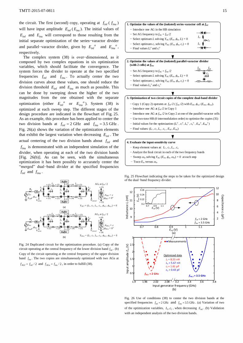
TMTT-2015-07-0811 15
the circuit. The first (second) copy, operating at inlf ( inuf ) will have input amplitude inlE ( inuE ). The initial values of
inlE and inuE will correspond to those resulting from the initial separate optimization of the series−varactor divider and parallel−varactor divider, given by o
inlE and oinuE ,
respectively. The complex system (38) is over−dimensioned, as it
composed by two complex equations in six optimization variables, which should facilitate the convergence. The system forces the divider to operate at the two specified frequencies inlf and inuf . To actually center the two division curves about these values, one should reduce the division threshold inlE and inuE as much as possible. This can be done by sweeping down the higher of the two magnitudes from the one obtained with the separate optimization (either o
inlE or oinuE ). System (38) is
optimized at each sweep step. The different stages of the design procedure are indicated in the flowchart of Fig. 25. As an example, this procedure has been applied to center the two division bands at 2 GHzinlf = and 3.5 GHzinuf = . Fig. 26(a) shows the variation of the optimization elements that exhibit the largest variation when decreasing inlE . The actual centering of the two division bands about inlf and
inuf is demonstrated with an independent simulation of the divider, when operating at each of the two division bands [Fig. 26(b)]. As can be seen, with the simultaneous optimization it has been possibly to accurately center the “merged” dual−band divider at the specified frequencies
inlf and inuf .
BA
Vvarac
cu
Lu
Rg
AGl at finl / 2
Vvarac2
cl cuLlLl
Lu
Lu
Lu
ΑAGl = εφAGl = 0°
Buffer
Buffer
BA
Vvarac
cu
Lu
Rg
AGu at finu / 2
Vvarac2
cl cuLlLl
Lu
Lu
Lu
Buffer
Buffer
ΑAGu = εφAGu = 0°
YAGl = (Ll , cl , Lu , cu , φin,l , φin,u ) = 0
finl
Einle jφin,l
finu
Einue jφin,u
YAGu = (Ll , cl , Lu , cu , φin,l , φin,u ) = 0
v+(1) v+(2) v+(3) v+(4) v+(5)
v−(5)v−(4)v−(3)v−(2)v−(1)
v+(1) v+(2) v+(3) v+(4) v+(5)
v−(5)v−(4)v−(3)v−(2)v−(1)
v+(3)
v−(3)
v+(4)
v−(4)
Fig. 24 Duplicated circuit for the optimization procedure. (a) Copy of the circuit operating at the central frequency of the lower division band inlf . (b) Copy of the circuit operating at the central frequency of the upper division band inuf . The two copies are simultaneously optimized with two AGs at
/ 2AGl inlf f= and / 2AGu inuf f= , in order to fulfill (38).
1. Optimize the values of the (isolated) series-varactor cell at finl
− Introduce one AG in the HB simulation− Set AG frequency to fAG = finl /2 − Select optimum L solving YAG (Ein, φin, L) = 0
− Final values Llo and cl
o
Llcl
Ll− Select optimum cc solving YAG (Ein, φin, cc) = 0
2. Optimize the values of the (isolated) parallel-varactor divider (with 2 cells) at finu
− Set AG frequency to fAG = finu /2 − Select optimum L solving YAG (Ein, φin, L) = 0
− Final values Luo and cu
o− Select optimum cc solving YAG (Ein, φin, cc) = 0
3. Optimization of two circuit copies of the complete dual-band divider
− Copy 1 (Copy 2) operates at finl /2 ( finu /2) with Einl, φin,l (Einu, φin,u).− Introduce one AG at finl /2 in Copy 1 − Introduce one AG at finu /2 in Copy 2 at one of the parallel-varactor cells− Use two-tone HB (0 intermodulation order) to optimize the copies (35) − Initial values for the optimization (Ll
o , clo , Lu
o , cuo , Einl
o , Einuo )
− Final values: (Ll , cl , Lu , cu , Einl
, Einu)
4. Evaluate the input-sensitivity curve
− Analyze the final circuit in each of the two frequency bands− Keep element values at: Ll , cl
, Lu , cu
− Sweep ωin solving YAG (Ein, φin, ωin) = 0 at each step − Trace Ein versus ωin
cu
Lu Lu
Fig. 25 Flowchart indicating the steps to be taken for the optimized design of the dual−band frequency divider.
0.5
1
1.5
2
2.5
3
Input generator frequency (GHz)
Inpu
t am
plitu
de E
in (V
)
3.2 3.4 3.6 3.81.9 1.96 2.02 2.08
Optimized data
0.7 0.8 0.9 1 1.1
9
10
11
12 Capacitance cl (pF)2
4
6
8
10
12
0.2
0.22
0.24
0.26
0.7 0.9 1.1
Measurements
Fig. 26 Use of conditions (38) to center the two division bands at the specified frequencies 2 GHzinlf = and 3.5 GHzinuf = . (a) Variation of two
of the optimization variables, ,l lL c , when decreasing inlE . (b) Validation with an independent analysis of the two division bands.
TMTT-2015-07-0811 16
V. CONCLUSION A design methodology for a recently proposed
frequency−divider configuration based on varactor−inductor cell has been proposed. The method derives from an initial analytical study of a single−cell divider, which provides insight into the impact of the various circuit elements on the input−amplitude threshold and the frequency bandwidth. The inductors of the divider topology enable the shift of the frequency−division band and an additional capacitor enables the reduction of the input−amplitude threshold. With a higher number of cells, the two element types still enable these two separate actions, as has been verified with a full harmonic balance analysis, using an auxiliary generator at the divided frequency. Two different applications have been demonstrated: a dual−phase divider, based on the use of a Marchand balun, and a dual−band frequency divider, based on a novel configuration in which a series−varactor cell is embedded between two parallel−varactor cells. A simple synthesis method is presented to center the two division bands at the desired values. The techniques have been applied to three prototypes at 2.15 GHz, 1.85 GHz and 1.75 GHz / 3.95 GHz, respectively.
REFERENCES
[1] W. Lee and E. Afshari, "Low−Noise Parametric Resonant Amplifier," IEEE Trans. Circuits and Systems I, vol.58, no.3, pp.479−492, Mar., 2011.
[2] W. Lee and E. Afshari, "Distributed Parametric Resonator: A Passive CMOS Frequency Divider," IEEE J. Solid−State Circuits, vol.45, no.9, pp.1834−1844, Sept., 2010.
[3] H. R. Rategh and T. H. Lee, “Superharmonic injection−locked frequency dividers,” IEEE J. Solid−State Circuits, vol. 34, no. 6, pp. 813–821, Jun. 1999.
[4] R. Quere, E. Ngoya, M. Camiade, A. Suérez, M. Hessane, and J. Obregón, “Large signal design of broadband monolithic microwave frequency dividers and phase−locked oscillators,” IEEE Trans. Microwave Theory Techn., vol. 41, pp. 1928–1938, Nov. 1993.
[5] A. Suárez, J.C. Sarkissian, R. Sommet, E. Ngoya, and R. Quere, "Stability analysis of analog frequency dividers in the quasi−periodic regime," IEEE Microw. Guided Wave Lett., vol.4, no.5, pp.138–140, May 1994.
[6] A. Suárez, R. Quéré, Stability Analysis of Nonlinear Microwave Circuits. Boston, MA: Artech House, 2003.
[7] A. Suárez, Analysis and Design of Autonomous Microwave Circuits. Hoboken, NJ: Wiley IEEE Pres, 2009.
[8] F. Ramírez, M. Pontón, S. Sancho, A. Suárez, “Phase−Noise Analysis of Injection−Locked Oscillators and Analog Frequency Dividers”, IEEE Trans. Microw. Theory Techn., vol. 56, no.2, pp. 393−407, 2008.
[9] S. Qin, Q. Xu and Y. E. Wang, “Nonreciprocal Components With Distributedly Modulated Capacitors,” IEEE Trans. Microw. Theory Techn., vol. 62, no. 10, pp. 2260– 2272, Oct.2014.
[10] M. Pontón and A. Suárez, “Analysis of a frequency divider by two based on a differential nonlinear transmission line,” IEEE MTT−S Int. Microw. Symp. Dig., Phoenix, AZ, USA, 2015, pp.1−3.
[11] S.A. Kian and I.D. Robertson, "Analysis and design of impedance−transforming planar Marchand baluns," IEEE Trans. Microw. Theory Techn., vol.49, no.2, pp.402−406, Feb., 2001.
[12] L. Zhang and H. Wu, "A double−balanced injection−locked frequency divider for tunable dual−phase signal generation," IEEE Radio Frequency Integrated Circuits (RFIC) Symposium, San Francisco, CA., 2006.
[13] V. Arana, A. Suarez, P. Dorta, "Dual−band frequency divider based on oscillation control," IEEE MTT−S Int. Microw. Symp. Dig., Fort Worth, TX, USA, Jun. 2004, vol.3, pp.1501−1504.
[14] J. Guckehnehimer and P. Holmes, Nonlinear Oscillations, Dynamical Systems, and Bifurcations of Vector Fields, Springer Verlag, NY, 1983.
[15] [Online].Available:http://www.skyworksinc.com/uploads/documents/SMV123x_Series_200058V.pdf
[16] F. Ramírez, E. de Cos, and A. Suárez, “Nonlinear analysis Tools for the Optimized Design of Harmonic−Injection Dividers,” IEEE Trans. on Microwave Theory and Techn., vol. 51, no. 6, pp. 1752–1762, Jun., 2003.
[17] K. Kurokawa, “Noise in synchronized oscillators,” IEEE Trans. Microw. Theory Techn., vol. 16, no. 4, pp. 234–240, Apr., 1968.
[18] J.M. Paillot, J.C. Nallatamby, M. Hessane, R. Quere, M. Prigent and J. Rousset, “A general program for steady state, stability, and FM noise analysis of microwave oscillators,” IEEE MTT−S Int. Microwave Symp. Dig., Dallas, TX, USA, 1990, pp. 1287–1290.
[19] V. Rizzoli, F. Mastri, and D. Masotti, “General noise analysis of nonlinear microwave circuits by the piecewise harmonic−balance technique,” IEEE Trans. Microw. Theory Techn., vol. 42, no. 5, pp. 807–819, May 1994.
[20] Y. Park, S. Chakraborty, C.−H. Lee, S. Nuttinck, J. Laskar, "Wide−band CMOS VCO and frequency divider design for quadrature signal generation," IEEE MTT−S Int. Microw. Symp. Dig., Fort Worth, TX, USA, Jun. 2004, vol.3, pp.1493−1496.
[21] J. Jugo, J. Portilla, A. Anakabe, A. Suárez and J.M. Collantes, “Closed–loop stability analysis of microwave amplifiers,” IEEE Electron. Lett., vol. 37, no. 4, pp. 226−228, 2001.
Mabel Pontón (S’08–M’11) was born in Santander, Spain. She received the Telecommunication Engineering degree from the University of Cantabria, Spain in 2004, Masters in Information Technologies and Wireless Communications Systems and Ph.D. degree from the University of Cantabria, Santander, Spain, in 2008 and 2010, respectively. In 2006, she joined the Communications Engineering Department of
University of Cantabria. From 2011 to 2013 she was with the Group of Electronic Design and
Applications (EDA) at Georgia Institute of Technology, Atlanta, GA as a Post−Doctoral Research Fellow. Her research interests are focused on the nonlinear analysis and simulation of radiofrequency and microwave circuits, with emphasis on phase−noise, stability and bifurcation analysis of complex oscillator topologies.
Almudena Suárez (M’96–SM’01–F’12) was born in Santander, Spain. She received the Electronic Physics and Ph.D. degrees from the University of Cantabria, Santander, Spain, in 1987 and 1992, respectively, and the Ph.D. degree in electronics from the University of Limoges, Limoges, France, in 1993.
She is currently a Full Professor with the Communications Engineering Department, University of Cantabria. She co−authored Stability
Analysis of Nonlinear Microwave Circuits (Artech House, 2003) and authored Analysis and Design of Autonomous Microwave Circuits (IEEE−Wiley, 2009).
Prof. Suárez is a member of the Technical Committees of the IEEE Microwave Theory and Techniques Society (IEEE MTT−S) International Microwave Symposium (IMS) and the European Microwave Conference. She was an IEEE Distinguished Microwave Lecturer from 2006 to 2008. She is a member of the Board of Directors of the European Microwave Association. She is the Editor−in−Chief of the International Journal of Microwave and Wireless Technologies (Cambridge University Press). She was the co−chair of IEEE Topical Conference on RF Power Amplifiers (PAWR) in 2014 and 2015.