Embed Size (px)
Citation preview

DRAG ICA VAS I L E S KA
OPTIMIZE SOLAR CELL
PERFORMANCE

MINIMIZE LOSSES IN SOLAR CELLS
Optical loss
Electrical Loss
Concentration of light
Minimize Shadowing
Trapping of light:
AR coatings Mirrors ( metallization rear surface or growing
active layers on top of a Bragg stack)
textured surface
Photon recycling
reabsorption of photons emitted by radiative recombination inside the cell
Surface passivation
Resistive loss
……

OPTICAL LOSS

CONCENTRATION OF LIGHT


MINIMIZE SHADOWING
• Light enters through the window normal to the top surface defined by
the metal contact.
• No carriers are generated by the light under the metal contact as it is
reflected back.
• Carriers generated by light entering through the window diffuse to the
region below the metal contact due to density gradient. These carriers
generated near the space charge region contribute to the current
produced by the solar cell.
• Surface recombination takes place on the surface of the window which
reduces the efficiency of the solar cell.


ADVANCED METALIZATION
Prevent obscuration of the solar cell or high reflection and absorption of the silver grids.
small and high grids, which will become smaller towards the edge of the cell
COSIMA (Contacts to a-Si:H passivated wafers
by means of annealing):
Amorphous silicon (silane process) on mono-
crystalline silicon
Aluminium on theses layers results in
contacting the monocrystalline silicon
Process temperature ~ 200°C
No photolithographySolar cell with a-Si:H-rear passivation and COSIMA contacts

Advantages: Simplifies thin film manufacturing process
Efficiency values about 20%
Combination with doted contacts: Screen printed interface layer (little holes) good passivation
Aluminium on the interface layer COSIMA
Advantages: Can be used on thinner wafers no bending
The passivation abbility of the amorphous layer will be kept after the annealing process
The contact resistivity is 15mΩcm2
Increase of the quantum yield in the infrared wavelength range
Reduces Seff to 100 cm/s (4% metallization)

EWT/MWT
Front (left) and rear (right) of a EWT-solar cell. The front contacts
are brought to the rear of the solar cell by many dots.
Emitter Wrap through (EWT)
• Emitter on the front surface is wraped with the rear surface by little holes
• Edges of the holes are also emitter areas, which transport emitter current
• Power-conveying busbars and the grid are moved to the rear surface
• Use double sided carrier collection (n+pn+) increases the efficiency
• 100µm holes are made by laser
EWT- cell with n+pn+ - structure

Disadvantage:Manufacturing process is very complex
Metal wrap throug (MWT)
• Absence of the bus bars (on the rear side) connection by holes
• Less serial resistance losses because of interconnection of the moduleson the back
• FF ~77%; efficiency ~ 16%
Advantages:• Eliminate grid obscuration no high doping high Isc high efficiency
• n+pn+- structure use lower quality solar grade silicon
• Uniform optical appereance improves asthetics
• Silicon solar cell < 200μm
• Efficiency around 18%
• gain in active cell area
•Diffusion length can be reduced to the half
MWT-cell

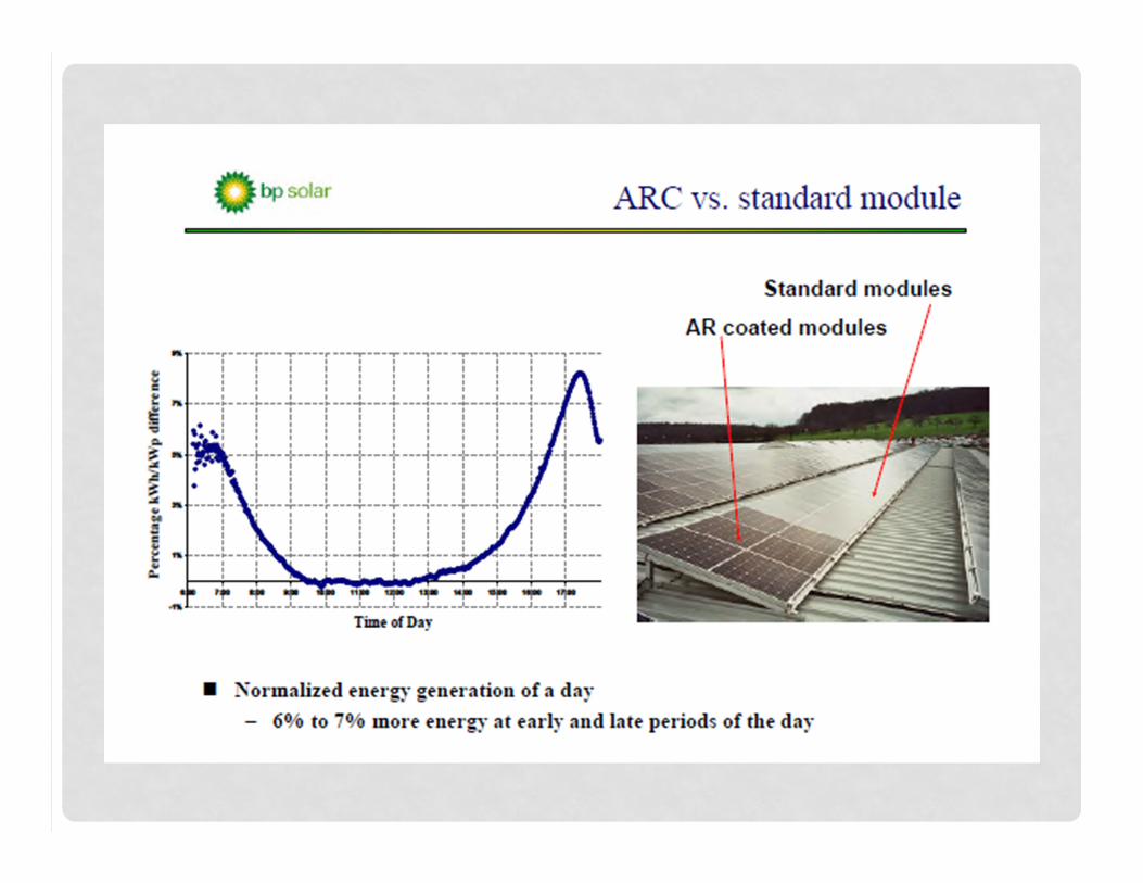
TRAPPING OF LIGHT:
ANTI-REFLECTION COATINGS
• Antireflection Coatings
Anti-reflection coatings on solar cells are similar to those used on other optical equipment such as camera lenses. They consist of a thin layer of dielectric material, with a specially chosen thickness so that interference effects in the coating cause the wave reflected from the anti-reflection coating top surface to be out of phase with the wave reflected from the semiconductor surfaces. These out-of-phase reflected waves destructively interfere with one another, resulting in zero net reflected energy.


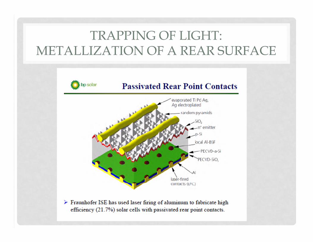
TRAPPING OF LIGHT:
METALLIZATION OF A REAR SURFACE

TRAPPING OF LIGHT:
TEXTURED SURFACE


advantages:
At least second reflection
The effective absorption length of the silicon layer will bereduced the light way through the layer increases
The area of the surface becomes bigger
Total reflection on the inside of the front layer possible
Reflection can be reduced about 9/10 of the former reflection
Examples of light trapping

PHOTON RECYCLING
• The re-absorption of photons emitted in a semiconductor material as a consequence of radiativerecombinations, a process referred to as photon recycling (PR), has been researched into for several decades because of its primary influence in increasing the minority carrier lifetime and related parameters.
• Solar cells with direct bandgap materials and high-absorption coefficients are firm candidates to show PR effects, leading to an improvement in the conversion efficiency of up to 1-2% in absolute terms for cells with conventional designs.
• However, the formal modeling of PR effects requires the inclusion of additional terms in the standard set of semiconductor equations and researchers usually tend to neglect its influence, because of the lack of available tools for an easy evaluation of this phenomenon in their particular devices.

ELECTRICAL LOSS

29
SURFACE PASSIVATION:
MOTIVATION
• For solar cells to be able to compete with other electricity sources, $/Watt needs to be reduced:
• Improve efficiency
• Reduce production cost
• For high-efficiency cells, good front and back surface passivation is mandatory

30
INTRODUCTION
• Surface recombination velocity (SRV) is the figure of merit for passivation quality• Lower is better
• Below 200 cm/s is decent
BulkEmitter
n+ p
Front
Light
Back
e- e- e- e-
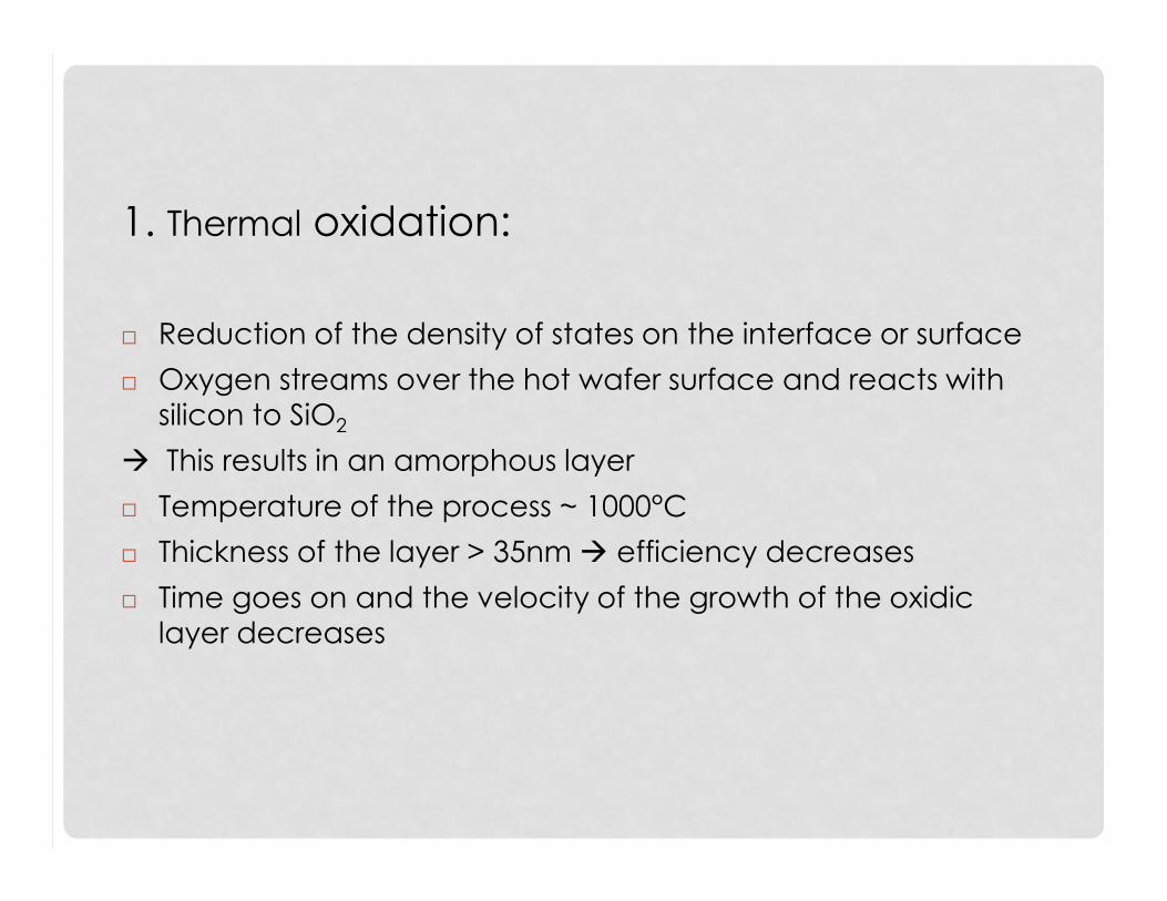
1. Thermal oxidation:
Reduction of the density of states on the interface or surface
Oxygen streams over the hot wafer surface and reacts with silicon to SiO2
This results in an amorphous layer
Temperature of the process ~ 1000°C
Thickness of the layer > 35nm efficiency decreases
Time goes on and the velocity of the growth of the oxidic layer decreases

2. Passivation with SiNx
Reduction of the density of states on the interface
Gases silane SiH4 and methane NH3 form a layer of Si3N4
Temperature of the process ~ 350°C
Passivation quality rises with silane amount
S ~ 20 cm/s – 240 cm/s depending on the refraction index
advantages:
lower production temperature
Nitride seems also to work better as an anti reflection layer for solar cells
better passivation

3. Passivation with only silane
The quality of the passivation is enormous
Passivation layer on the emitter should be very thin (10nm)
high absorption prefer SiNx-Process on the emitter
The process temperature is ~225°C
The passivation seems independet of contaminations of the silicon surface brought in during the manufacturing process
An example is the HIT-Solar Cell from Sanyo
Layer of monocristalline silicon between amorphous silicon layers
Efficiency of ~ 18,5%
Passivierqualität als Funktion der a-Si:H-Schichtdicke
HIT solar cell

4. Back Surface Field (BSF)
A thin layer of p-doped material to prevent the minorities from moving to the back contact where they recombinate
e.g. use aluminium for a back contact, which melts (T ~ 500°C) into the silicon and creates a positive doped BSF. Besides it serves as a reflection layer.

35
PROCEDURE: 4 STEPS
Choose the basic passivation methods
Achieve decent quality of passivation on each of the chosen methods
Apply the methods on actual solar cells
Assess SRV

36
CHOOSE THE BASIC PASSIVATION
METHODS
• Three basic methods for passivation were chosen
Method Mechanism
1. Al-back surface field
(Al-BSF)Creates an electric field that pushes carriers away
from the surface2. Boron-BSF
3. Dielectric passivationReduces trap levels at the
surface
Step 1:

37
ACHIEVE DECENT QUALITY OF
PASSIVATION ON EACH OF THE
CHOSEN METHODS
• Al-BSF
• Method for uniform Al-BSF was established
• SRV of 230 cm/s was obtained
• Dielectric passivation
• RTO/LF-SiNx provided the best passivation
• SRV of 51 cm/s was obtained by RTO/LF-SiNx
(without electrical contacts)
• Boron-BSF
• Results indicated promisingly low SRV
Step 2:
38
APPLY THE METHODS ON ACTUAL
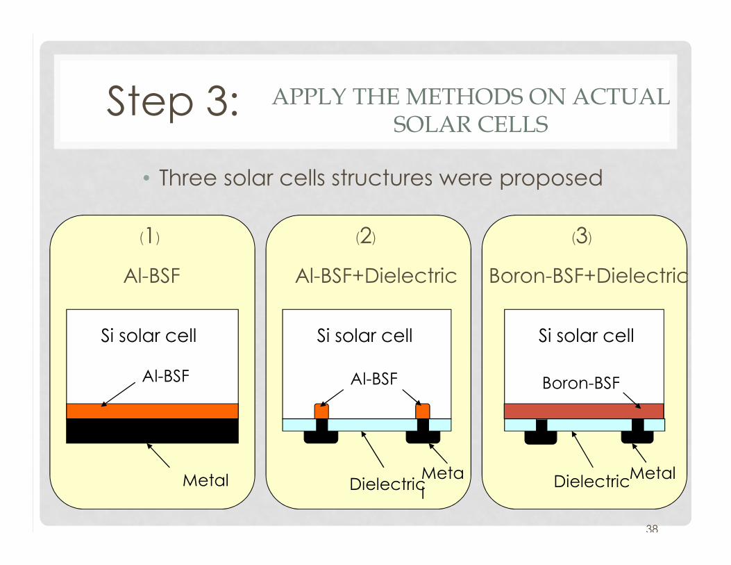
SOLAR CELLS
• Three solar cells structures were proposed
Step 3:
Si solar cell
Al-BSF
Metal
(1)
Al-BSF
Dielectric
Si solar cell
Al-BSF
Metal
(2)
Al-BSF+Dielectric
Dielectric
Si solar cell
Boron-BSF
Metal
(3)
Boron-BSF+Dielectric

39
STEP 4:
• SRV can be obtained by measuring IQE and bulk lifetime
Long-wavelengthinternal quantum efficiency (IQE)
SRV of the back surface Bulk lifetime
Assess SRV
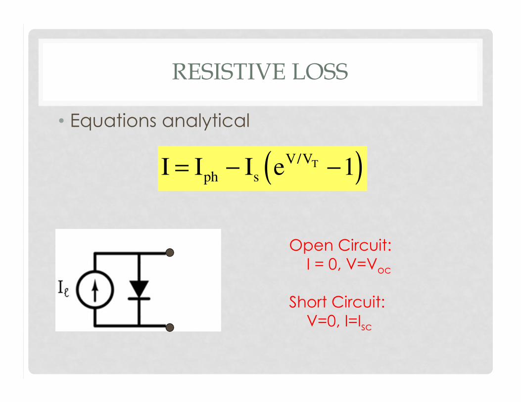
RESISTIVE LOSS
• Equations analytical
( )TV/V
ph sI I I e 1= − −
Open Circuit:I = 0, V=Voc
Short Circuit:V=0, I=Isc

Maximum power point (MMP)
depends on:
• Temperature
• Irradiance
• Solar cell characteristics
Wilson s. 209
Efficency coefficent
Performance of solar cell
Fill factor

Open Circuit:I = 0, V=Voc
Short Circuit:V=0, I=Isc
The power produced by the cell in Watts can be easily calculated along the I-V sweep by the equation P=IV. At the ISC and VOCpoints, the power will be zero and the maximum value for power will occur between the two. The voltage and current at this maximum power point are denoted as VMP and IMP respectively.

During operation, the efficiency of solar cells is reduced by the dissipation of power across internal resistances. These parasitic resistances can be modeled as a parallel shunt resistance (RSH) and series resistance (RS).
For an ideal cell, RSH would be infinite and would not provide an alternate path for current to flow, while RS would be zero, resulting in no further voltage drop before the load.
Decreasing RSH and increasing Rs will decrease the fill factor (FF) and PMAX as shown in the figure on the next slide. If RSH is decreased too much, VOC will drop, while increasing RS excessively can cause ISC to drop instead.

Decrease in the FF due to RS and RSH.

It is possible to approximate the series and shunt resistances, RS and RSH, from the slopes of the I-V curve at VOC and ISC, respectively. The resistance at Voc, however, is at best proportional to the series resistance but it is larger than the series resistance. RSH is represented by the slope at ISC. Typically, the resistances at ISC and at VOC will be measured and noted.