Embed Size (px)
Citation preview
Optimization of High and Anti-reflective Facet Coating
for Near Infrared High Power Laser Diode
Seung Jin Lee1,1,Hee Jo An1, Taeksoo Ji*
1 Department of Electronics and Computer Engineering,
Chonnam National University, Gwangju 500-757, Korea, *[email protected]
Abstract. The output and efficiency of laser diode can be changed by single or
multi-layer thin film coating having different refractive indices. In this research,
laser diode is coated with single layer Anti-reflection (AR) coating of Al2O3
and Multi-layer High-reflection (HR) coating of SiO2/Ta2O5. Thin film was
deposited by ion beam assisted deposition (IAD) equipment after design
optimization. For the wavelength range of 850~1,100nm (near infrared
wavelength range), the transmittance of thin film coated front facet is 95% and
reflectance of the back facet is 90%. The output of laser diode is increased by
100% after facet AR/HR coating.
Keywords: Laser diode, Facet coating, Reflection, Al2O3, SiO2/Ta2O5
1 Introduction
Laser diode (LD) is used for a many applications in optical communication, medical
field, industry, printing and many other fields [1]. Recently, high power LD research
has received wide attention [2, 3]. One of important factor in fabrication technology
of high power LD is thin film coating. It is possible to make high quality thin film
coating by using Ion beam deposition technology. This improves the optical and
mechanical properties of the laser diode [4, 5]. While selecting the material for
AR/HR coating, many parameters such as wavelength band, transmittance, absorption
coefficient, deposition rate, refractive index must be considered [6].
In a typical experiment GaAs wafer based LD was used. Al2O3 (Aluminium oxide)
was found to be suitable material for front facet coating(AR). Al2O3 refractive index
is similar to commonly used SiO2 and does not cause the absorption of wavelength
300~5,000nm range. So, this material is suitable to be used as AR Coating. Back facet
HR coating is done using SiO2(Silicon dioxide)/Ta2O5(Tantalum pentoxide). Using
the multi-layer structure of different materials having different refractive indices, like
high refractive index of Ta2O5 and low refractive index of SiO2, the reflectance
increases [7, 8]. The comparison of output of LD before and after coating for
wavelength range 850~1,100nm has been done and report. In this paper, designed and
optimized single layer anti-reflection/high-reflection coating on laser diode.
Advanced Science and Technology Letters Vol.139 (EEC 2016), pp.418-421
http://dx.doi.org/10.14257/astl.2016.139.83
ISSN: 2287-1233 ASTL Copyright © 2016 SERSC
2 Experimental Details
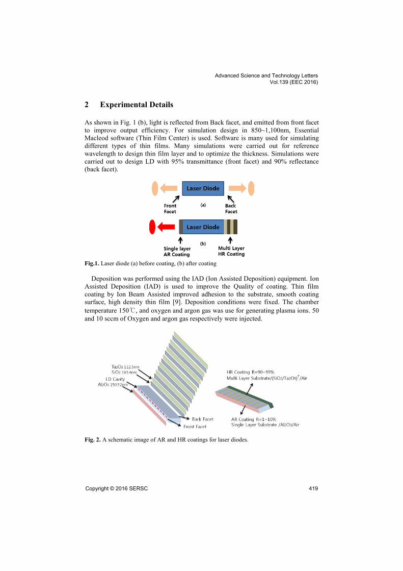
As shown in Fig. 1 (b), light is reflected from Back facet, and emitted from front facet
to improve output efficiency. For simulation design in 850~1,100nm, Essential
Macleod software (Thin Film Center) is used. Software is many used for simulating
different types of thin films. Many simulations were carried out for reference
wavelength to design thin film layer and to optimize the thickness. Simulations were
carried out to design LD with 95% transmittance (front facet) and 90% reflectance
(back facet).
Fig.1. Laser diode (a) before coating, (b) after coating
Deposition was performed using the IAD (Ion Assisted Deposition) equipment. Ion
Assisted Deposition (IAD) is used to improve the Quality of coating. Thin film
coating by Ion Beam Assisted improved adhesion to the substrate, smooth coating
surface, high density thin film [9]. Deposition conditions were fixed. The chamber
temperature 150℃, and oxygen and argon gas was use for generating plasma ions. 50
and 10 sccm of Oxygen and argon gas respectively were injected.
Fig. 2. A schematic image of AR and HR coatings for laser diodes.
Advanced Science and Technology Letters Vol.139 (EEC 2016)
Copyright © 2016 SERSC 419
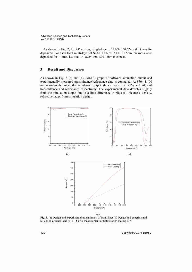
As shown in Fig. 2, for AR coating, single-layer of Al2O3 150.52nm thickness for
deposited. For back facet multi-layer of SiO2/Ta2O5 of 163.4/112.5nm thickness were
deposited for 7 times, i.e. total 14 layers and 1,931.3nm thickness.
3 Result and Discussion
As shown in Fig. 3 (a) and (b), AR/HR graph of software simulation output and
experimentally measured transmittance/reflectance data is compared. At 850~ 1,100
nm wavelength range, the simulation output shows more than 95% and 90% of
transmittance and reflectance respectively. The experimental data deviates slightly
from the simulation output due to a little difference in physical thickness, density,
refractive index from simulation design.
800 850 900 950 1000 1050 1100 1150 1200
0
20
40
60
80
100R
efle
cta
nce
(%
)
Wavelength (nm)
Experiment Reflectance (%)
Design Reflectance (%)
(a) (b)
0 200 400 600 800 1000 1200 1400 1600 1800 2000
0
200
400
600
800
1000
1200
1400
Po
we
r(m
W)
Current(mA)
Before coating
After Coating
(c)
Fig. 3. (a) Design and experimental transmission of front facet (b) Design and experimental reflection of back facet (c) P-I Curve measurement of before/after coating LD
800 850 900 950 1000 1050 1100 1150 1200
0
20
40
60
80
100
Tra
nsm
itta
nce
(%)
Wavelength (nm)
Design Transmittance(%)
Experiment Transmittance(%)
Advanced Science and Technology Letters Vol.139 (EEC 2016)
420 Copyright © 2016 SERSC
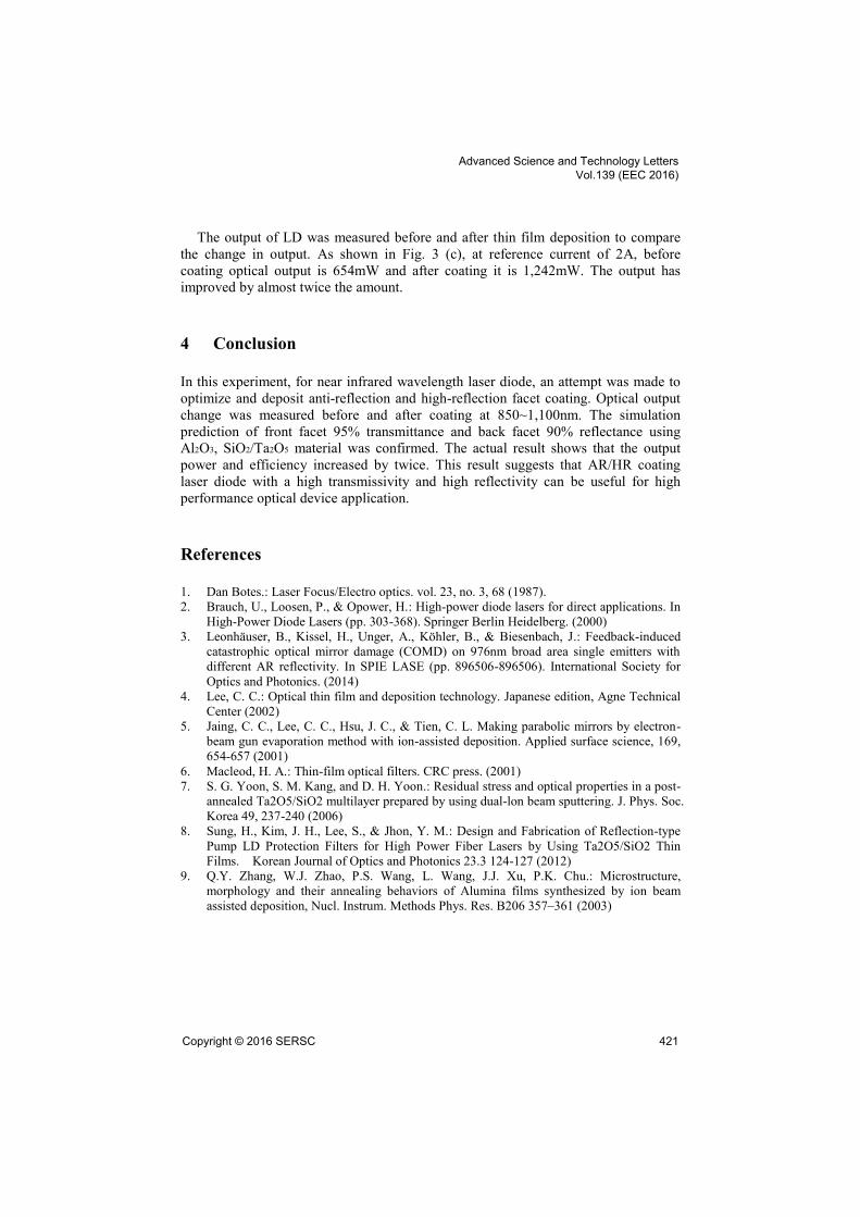
The output of LD was measured before and after thin film deposition to compare
the change in output. As shown in Fig. 3 (c), at reference current of 2A, before
coating optical output is 654mW and after coating it is 1,242mW. The output has
improved by almost twice the amount.
4 Conclusion
In this experiment, for near infrared wavelength laser diode, an attempt was made to
optimize and deposit anti-reflection and high-reflection facet coating. Optical output
change was measured before and after coating at 850~1,100nm. The simulation
prediction of front facet 95% transmittance and back facet 90% reflectance using
Al2O3, SiO2/Ta2O5 material was confirmed. The actual result shows that the output
power and efficiency increased by twice. This result suggests that AR/HR coating
laser diode with a high transmissivity and high reflectivity can be useful for high
performance optical device application.
References
1. Dan Botes.: Laser Focus/Electro optics. vol. 23, no. 3, 68 (1987).
2. Brauch, U., Loosen, P., & Opower, H.: High-power diode lasers for direct applications. In
High-Power Diode Lasers (pp. 303-368). Springer Berlin Heidelberg. (2000)
3. Leonhäuser, B., Kissel, H., Unger, A., Köhler, B., & Biesenbach, J.: Feedback-induced
catastrophic optical mirror damage (COMD) on 976nm broad area single emitters with
different AR reflectivity. In SPIE LASE (pp. 896506-896506). International Society for
Optics and Photonics. (2014)
4. Lee, C. C.: Optical thin film and deposition technology. Japanese edition, Agne Technical
Center (2002)
5. Jaing, C. C., Lee, C. C., Hsu, J. C., & Tien, C. L. Making parabolic mirrors by electron-
beam gun evaporation method with ion-assisted deposition. Applied surface science, 169,
654-657 (2001)
6. Macleod, H. A.: Thin-film optical filters. CRC press. (2001)
7. S. G. Yoon, S. M. Kang, and D. H. Yoon.: Residual stress and optical properties in a post-
annealed Ta2O5/SiO2 multilayer prepared by using dual-lon beam sputtering. J. Phys. Soc.
Korea 49, 237-240 (2006)
8. Sung, H., Kim, J. H., Lee, S., & Jhon, Y. M.: Design and Fabrication of Reflection-type
Pump LD Protection Filters for High Power Fiber Lasers by Using Ta2O5/SiO2 Thin
Films. Korean Journal of Optics and Photonics 23.3 124-127 (2012)
9. Q.Y. Zhang, W.J. Zhao, P.S. Wang, L. Wang, J.J. Xu, P.K. Chu.: Microstructure,
morphology and their annealing behaviors of Alumina films synthesized by ion beam
assisted deposition, Nucl. Instrum. Methods Phys. Res. B206 357–361 (2003)
Advanced Science and Technology Letters Vol.139 (EEC 2016)
Copyright © 2016 SERSC 421