Embed Size (px)
Citation preview

Optimization ofdown-conversion phosphorfilms for high efficiency whiteorganic light-emitting diodes
Debasis BeraSergey MaslovJaewon LeeJiangeng XueFranky SoPaul H. Holloway
Downloaded From: https://www.spiedigitallibrary.org/journals/Journal-of-Photonics-for-Energy on 5/18/2018 Terms of Use: https://www.spiedigitallibrary.org/terms-of-use

Optimization of down-conversion phosphor films forhigh efficiency white organic light-emitting diodes
Debasis Bera, Sergey Maslov, Jaewon Lee, Jiangeng Xue, Franky So,and Paul H. Holloway
University of Florida, Department of Materials Science and Engineering,Gainesville, Florida 32601
Abstract. White light emitting devices were fabricated using blue emitting organic light emittingdiodes (OLEDs) and down-conversion phosphor mixtures. Three different thicknesses of yellowand mixtures of yellow and red luminescent phosphor films were prepared on separate glassslides using a silicone matrix. The down-conversion films were optimized by varying thethickness and phosphor to silicone weight ratio. The phosphor films with different thickness werecoupled to an optimized blue emitting OLED with a refractive index matching gel. Optimizeddown-conversion phosphor layers integrated with blue OLEDs exhibited 2× enhancement ofefficiency (lumens per electrical Watt) for white to that of the blue OLED. The InternationalCommission of Illumination color coordinates and average color rendering index for this devicewere (0.43, 0.46) and >80, respectively. C© 2011 Society of Photo-Optical Instrumentation Engineers
(SPIE). [DOI: 10.1117/1.3642643]
Keywords: light-emitting diodes; organic light-emitting diodes; phosphor; white light; down-conversion; color rendering index; color coordinates.
Paper 10118SSPRRR-Appeal received Aug. 2, 2010; revised manuscript received Aug. 26,2011; accepted for publication Aug. 29, 2011; published online Dec. 1, 2011.
1 Introduction
The light-emitting diode (LED), an emerging and energy efficient lighting technology, is ex-pected to significantly reduce global energy consumption and green-house emission.1 By usingwhite LEDs, the Department of Energy recently has put forward a target to reduce the totalhousehold lighting energy usage by 50% by 2025. Currently, a tremendous amount of effort hasbeen directed toward research on two types of white LEDs: 1. intrinsically generated white lightfrom LEDs and 2. down-conversion of high energy light to white using a phosphor layer. Theintrinsically generated white light from the LED is produced from a single or multi-emittinglayered LED device,2,3 whereas a down-converted white light is generated from the LED withsingle or multiple phosphor/s. An ultraviolet (380 to 400 nm)4–7 or a blue (440 to 480 nm)light8–11 is generally used for the down-conversion. For the blue light-based down-conversionstudies, an organic LED (OLED)12–14 or an inorganic LED (iLED)15–18 are used where a fractionof blue light is absorbed by the phosphor layer and re-emitted as lower energy photons. Thecombination of the blue and the lower energy photons produces white light. Use of the OLEDblue devices is advantageous to develop large area white light emitting devices for use as generalpurpose lighting and backlights for liquid crystal display.
This research is focused on optimization of the down-conversion phosphor layer for efficientand high quality white light emission using the blue OLEDs. This includes characterization ofphosphors, phosphor films, and film-incorporated devices to enhance the luminance efficacyand quality of white light. In this research, combinations of blue emitting OLEDs and yellow
1947-7988/2011/$25.00 C© 2011 SPIE
Journal of Photonics for Energy 011025-1 Vol. 1, 2011
Downloaded From: https://www.spiedigitallibrary.org/journals/Journal-of-Photonics-for-Energy on 5/18/2018 Terms of Use: https://www.spiedigitallibrary.org/terms-of-use

Bera et al.: Optimization of down-conversion phosphor films for high-efficiency...
phosphor or mixture of yellow and red phosphors for the down-conversion studies were used.We optimized the film thickness and phosphor loading to increase out-coupling efficiency ofwhite light. The optimized device showed a two times improvement in luminance efficacy forwhite light compared to blue luminance. A combination of yellow and red phosphor exhibiteda high quality white light.
2 Experimental
2.1 Preparation of Phosphor Films on Glass
Yellow (OY) and red (MR) phosphors were acquired from two commercial vendors. The yellowemitting OY phosphor is a cerium doped yttrium gadolinium garnet-based phosphor, whereasthe red emitting MR phosphor is based on europium doped nitrido silicate. For preparation ofphosphor thin-films, a silicone gel (LS-3354, NuSil Technology) was used as a matrix. Thesilicone gel (viscosity: 5400 cP) was prepared by mixing two uncured parts of transparent gelsat a weight ratio of 1:1. The refractive index of the film was found to be a slight function ofwavelength (1.577 at 411 nm to 1.547 at 589 nm). To optimize the loading of phosphor insilicone, films were prepared by varying the weight of the phosphor(s) in 150 mg of siliconegel. The films were prepared with 20, 30, 40, or 50 mg of OY phosphor in silicone. Similarly,the OY and MR red phosphor mixture at a weight ratio of 2:1 in silicone was used to prepareyellow-red phosphor film samples. Our previous results19 showed that the weight ratio of 2:1for yellow to red phosphor yielded an average color rendering index (CRI) or Ra value of 90when excited at 460 nm. The phosphor-silicone gel mixtures were manually doctor-bladed ontothe glass substrates (25 mm × 25 mm) followed by curing the film at 70◦C for 1 h in an oven.The curing of the films also facilitates a large range of operating temperatures: −40◦C to 200◦C.
2.2 Characterization of Phosphor and Phosphor Films
For particle size and morphological analyses of the phosphor, a scanning electron microscope(SEM JEOL JSM 6400) was used with an accelerating voltage of 15 kV. The phosphor dis-persed films were also characterized by the SEM. Photoluminescence (PL) and photolumines-cence excitation (PLE) spectra were acquired using a JASCO spectrophotometer (FP6500).The spectrophotometer also has a 60 mm diameter integrating sphere and the combination wasused to characterize optical properties of films, light sources, and white light. Transmissioncharacteristics (400 to 700 nm) of films, International Commission of Illumination (CIE) colorcoordinates of sources, phosphors and white light, internal quantum yield (QY) of phosphors,and CRI values of white lights were evaluated or determined using the spectrophotometer. Forthe QY measurement of phosphor, a blank substrate (cured 150 mg silicone without phosphor)and a sample with 30 mg of OY or MR phosphor and 150 mg silicone were used. Thickness ofthe phosphor films was measured using a profilometer (Tencor P2 Long Scan) at four differentspots on a diagonal scratch.
For the OLED characterization, the power was supplied by a Keithley power supply (2400Sourcemeter). The OLED with or without phosphor film was placed flush with an apertureof the integrating sphere to collect the light [see Fig. 1(a)]. The luminance values were ac-quired from the phosphor-loaded and the blank films at different operating powers. For down-conversion studies, silicone gel-phosphor mixtures were directly deposited on the glass-side ofthe OLED followed by curing in the oven at 70◦C for 1 h. A schematic structure of a down-conversion device is illustrated in Fig. 1(b). The structure of the OLEDs is discussed in Sec. 3.4 indetail.
Journal of Photonics for Energy 011025-2 Vol. 1, 2011
Downloaded From: https://www.spiedigitallibrary.org/journals/Journal-of-Photonics-for-Energy on 5/18/2018 Terms of Use: https://www.spiedigitallibrary.org/terms-of-use

Bera et al.: Optimization of down-conversion phosphor films for high-efficiency...
Fig. 1 Schematics show (a) the placement of the OLED on the integrating sphere, and(b) structure of a phosphor film integrated OLED device (ITO: indium tin oxide). The diagramsare not to scale.
3 Analysis and Optimization
3.1 Particle and Film Analysis
The SEM micrographs of as-received OY and MR phosphor particles are shown in Figs. 2(a)and 2(b), respectively. For the OY phosphor, the size distribution of individual particles rangesfrom 0.5 to 10 μm. The agglomerated size was found to be as high as 50 μm. For the MR
Fig. 2 SEM micrograph of (a) OY yellow phosphor, (b) MR red phosphor, and (c) cross-sectionof a phosphor film prepared using 30 mg of OY phosphor and 150 mg of silicone. (d) A highermagnification view of the film shown in (c).
Journal of Photonics for Energy 011025-3 Vol. 1, 2011
Downloaded From: https://www.spiedigitallibrary.org/journals/Journal-of-Photonics-for-Energy on 5/18/2018 Terms of Use: https://www.spiedigitallibrary.org/terms-of-use
Bera et al.: Optimization of down-conversion phosphor films for high-efficiency...
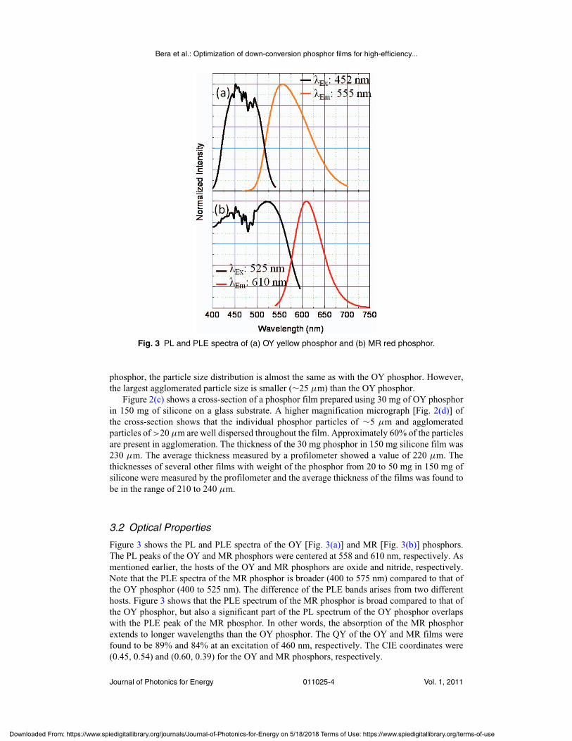
Fig. 3 PL and PLE spectra of (a) OY yellow phosphor and (b) MR red phosphor.
phosphor, the particle size distribution is almost the same as with the OY phosphor. However,the largest agglomerated particle size is smaller (∼25 μm) than the OY phosphor.
Figure 2(c) shows a cross-section of a phosphor film prepared using 30 mg of OY phosphorin 150 mg of silicone on a glass substrate. A higher magnification micrograph [Fig. 2(d)] ofthe cross-section shows that the individual phosphor particles of ∼5 μm and agglomeratedparticles of >20 μm are well dispersed throughout the film. Approximately 60% of the particlesare present in agglomeration. The thickness of the 30 mg phosphor in 150 mg silicone film was230 μm. The average thickness measured by a profilometer showed a value of 220 μm. Thethicknesses of several other films with weight of the phosphor from 20 to 50 mg in 150 mg ofsilicone were measured by the profilometer and the average thickness of the films was found tobe in the range of 210 to 240 μm.
3.2 Optical Properties
Figure 3 shows the PL and PLE spectra of the OY [Fig. 3(a)] and MR [Fig. 3(b)] phosphors.The PL peaks of the OY and MR phosphors were centered at 558 and 610 nm, respectively. Asmentioned earlier, the hosts of the OY and MR phosphors are oxide and nitride, respectively.Note that the PLE spectra of the MR phosphor is broader (400 to 575 nm) compared to that ofthe OY phosphor (400 to 525 nm). The difference of the PLE bands arises from two differenthosts. Figure 3 shows that the PLE spectrum of the MR phosphor is broad compared to that ofthe OY phosphor, but also a significant part of the PL spectrum of the OY phosphor overlapswith the PLE peak of the MR phosphor. In other words, the absorption of the MR phosphorextends to longer wavelengths than the OY phosphor. The QY of the OY and MR films werefound to be 89% and 84% at an excitation of 460 nm, respectively. The CIE coordinates were(0.45, 0.54) and (0.60, 0.39) for the OY and MR phosphors, respectively.
Journal of Photonics for Energy 011025-4 Vol. 1, 2011
Downloaded From: https://www.spiedigitallibrary.org/journals/Journal-of-Photonics-for-Energy on 5/18/2018 Terms of Use: https://www.spiedigitallibrary.org/terms-of-use

Bera et al.: Optimization of down-conversion phosphor films for high-efficiency...
Fig. 4 Transmission spectra in the visible range for films with different weight of OY phosphor inthe 150 mg of silicone matrix.
3.3 Transmission Study of Films
For transmittance measurements, samples were placed on an aperture of the integrating sphere tocollect all of the transmitted light. Transmission data showed that silicone did not absorb light inthe visible region. However, with an increased weight of the phosphor in the silicone matrix, thetransmission gradually decreased. Figure 4 shows the percent transmission versus wavelengthfrom the films with different weight of the OY phosphor in 150 mg of silicone. Approximately60% to 65% and 65% to 70% transmission were observed from the samples containing 30 and20 mg of phosphor in matrix, respectively. For 40 and 50 mg of phosphor film samples, thetransmissions decrease to 55% 60%. The trough in the transmission between 400 and 525 nmin Fig. 4 is due to absorption of light by the phosphor. The transmission values were reducedbetween 525 and 700 nm probably due to optical scattering by the phosphor particles. Since20 and 30 mg OY phosphor in silicone shows more than 60% transmission, these phosphormixtures will be used for the down-conversion study.
3.4 Characteristics of OLED
Two types of blue emitting OLEDs were used in this study: noncavity (NC) and microcavity(MC). The NC device contained no dielectric mirrors20 in between the indium doped tin oxide(ITO) and glass substrate [see Fig. 1(b)], whereas the MC devices contained two (2QWS) orfour layers of quarter wave stacks in between the ITO layer and glass. The structure of deviceswas ITO 50 nm//poly (3,4-ethylene-di-oxy-thiophene)–polystyrene-sulfonic acid (PEDOT:PSS)60 nm//1,1-bis[(di-4-tolylamino) phenyl] cyclohexane (TAPC) 25 nm//N,N′-dicarbazolyl-3,5-benzene (mCP) with 20 wt.% iridium (III) bis [(4,5-di-fluorophenyl)-pyridinato-N, C2′] pi-colinate (FIrPic)//4,7 diphenyl-1,10 phenanthroline and tris [3-3-(pyridyl)-mesityl] borane(3TPYMB) 40 nm//CsCO3 0.8 nm//Al 100 nm. The active area was 2 mm × 2 mm for all theOLED devices. See Refs. 20 and 21 for a detailed device structure and the fabrication processof the OLEDs. In this discussion, we have used data from NC and 2QWS MC blue emitting de-vices. The OLED device with NC exhibited a nearly Lambertian emission while 2QWS OLEDshave a more directional emission. We previously reported22 that down-converted light from ahighly directional blue emitting inorganic LED could yield a factor of 2 times enhancement inluminance efficacy.
The emission peaks from both NC and MC OLEDs were well within the broad peak ofthe PLE spectra of the phosphors (Fig. 3), therefore the blue light from the OLED was
Journal of Photonics for Energy 011025-5 Vol. 1, 2011
Downloaded From: https://www.spiedigitallibrary.org/journals/Journal-of-Photonics-for-Energy on 5/18/2018 Terms of Use: https://www.spiedigitallibrary.org/terms-of-use

Bera et al.: Optimization of down-conversion phosphor films for high-efficiency...
Fig. 5 (a) Color diagram and CIE coordinates for the OLEDs (round spot: noncavity and squarespot: 2 quarter wave stack microcavity) and phosphors (triangle: OY yellow and inverted triangle:MR). (b) Emission spectra from the two types of OLED: noncavity and microcavity with 2QWSstructure. (c) Voltage across the device to achieve various currents versus the number of runsshowing no degradation (active area: 2 mm × 2 mm). (d) Emission from an OLED before andafter baking.
partially absorbed by the phosphor/s and down-converted to yellow or yellow-red light. The CIEcoordinates of the OLED devices with cavity and noncavity structures were (0.154, 0.211) and(0.145, 0.271), respectively [see Fig. 5(a)]. Figure 5(b) shows the emission characteristicsfrom the two types of OLEDs. The macrocavity structure shifts the broader electrolumines-cence emission of FIrPic-doped OLED to a narrow blue emission. As mentioned earlier themicrocavity-based devices produce more directional emission compared to the noncavity de-vices. Therefore, down-conversion efficiency can be enhanced. Degradation of the OLED wasstudied over a range of current from 10 to 50 μA (size of active area of every device: 2 mm× 2 mm) for several consecutive runs as shown in Fig. 5(c). No degradation of the OLEDdevice occurred over 60 consecutive runs (∼1 min/run). However, a device operated at 1 mAdegraded by ∼6% during every run. Baking of the OLED device at 70◦C for 1 h caused animprovement of luminescence properties. Figure 5(d) shows electroluminescent spectra fromthe 2QWS device before and after baking of the device. Baking of polymer LEDs or PLEDs isreported to reduce the amount of radical ions generated during interactions of polymers. Theseions quenched the luminescence from the devices.23 Heat treatment of a vapor deposited organicfilm at higher temperature caused a higher crystallinity and higher carrier mobility as comparedto an as-deposited film.24,25 Data from this study suggest that better crystallinity improved thedevice performance.
3.5 Phosphor Optimization with OLEDs
Both MC and NC OLEDs were tested either bare or integrated with phosphor coated glassslides for down-conversion to white light. In down-conversion, yellow or yellow-red light from
Journal of Photonics for Energy 011025-6 Vol. 1, 2011
Downloaded From: https://www.spiedigitallibrary.org/journals/Journal-of-Photonics-for-Energy on 5/18/2018 Terms of Use: https://www.spiedigitallibrary.org/terms-of-use

Bera et al.: Optimization of down-conversion phosphor films for high-efficiency...
Fig. 6 Normalized down-converted spectra from blue OLED at 50 μA [(a) NC and (b) MC]integrated with bare glass or with phosphor films created by mixing 20, 25, or 30 mg of OYphosphor in 150 mg silicone. The NC OLED spectra were normalized at 465 nm, whereas theMC OLED spectra were at 463 nm.
the phosphor(s) mixed with nonabsorbed blue light from the OLED to provide white light.The schematic in Fig. 1(a) illustrates the configuration of the OLED and integrating sphere formeasurements of all the photons emitted at all angles. Since the 20 and 30 mg sample showedbetter transmission as compared to the 40 and 50 mg OY phosphor film (see Fig. 4), threephosphor films were prepared by mixing 20, 25, or 30 mg of the OY phosphor in 150 mg ofsilicone on three ∼20 μm thick glass slides.
After collecting five emission spectra from each bare blue OLED at currents from 50 μA,the same devices were combined with a phosphor layer and characterized for down-conversionof blue to white light. Each phosphor film was integrated with the NC or MC OLED using aglass index-matching-gel. Figures 6(a) and 6(b) show normalized emission spectra (∼465 nm)from bare and phosphor integrated NC OLED and MC OLED at a current of 50 μA. Figure 6shows that the emission peak from phosphor increases with an increasing amount of phosphor inthe film. Nonnormalized down-converted spectra showed that the blue emission decreased andemission from the phosphor increased with an increased amount of phosphor. Accordingly, theCIE coordinate shifts linearly from left to right in the CIE diagram with an increasing amountof the OY phosphor in the film: (0.231, 0.442), (0.244, 0.465), and (0.26, 0.485) for the 20,25, and 30 mg phosphor integrated NC device, respectively. The CRI values were found to beless than 45 for all samples. For the phosphor integrated MC device, the CIE coordinates alsofollowed the same trend as with NC devices. The CIE coordinates were (0.247, 0.445), (0.251,0.45), and (0.274, 0.492) for 20, 25, and 30 mg of phosphor, respectively. The CRI value is inthe range of 45 to 50. The white light from MC device exhibits better CRI values due to a largerFWHM of the emission peak compared to the NC device (see Fig. 6). Nevertheless, the 30 mgof phosphor in 150 mg of silicone exhibited a better quality of white light as compared to 20and 25 mg phosphor films. Therefore, the calculated efficacy will be compared for the 30 mgphosphor layers.
4 Down-Conversion Study
4.1 White Light Using Yellow Phosphors
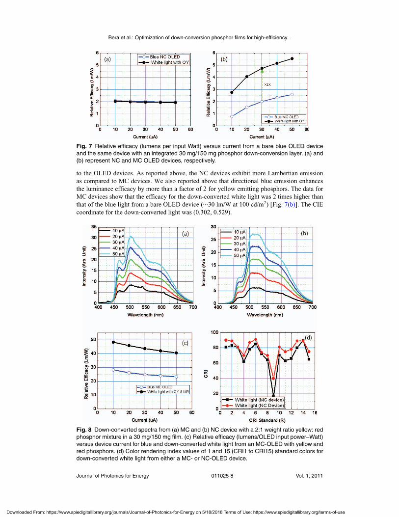
Figures 7(a) and 7(b) show the relative efficacies (lumens per OLED input Watt) versus driv-ing current to OLEDs for blue and down-converted white light from noncavity and micro-cavity devices, respectively. The efficacy values were compared in between bare blue anddown-conversion white using a photopic response curve. The absolute efficacy value of down-conversion was calculated to be 32 lm/W, whereas the bare blue emission was found to be 38lm/W at 100 cd/m2 (Ref. 26). Similarly, a relative efficacy, as shown in Fig. 7(a), shows noimprovement in down-converted white light from NC-OLED blue emission at different bias
Journal of Photonics for Energy 011025-7 Vol. 1, 2011
Downloaded From: https://www.spiedigitallibrary.org/journals/Journal-of-Photonics-for-Energy on 5/18/2018 Terms of Use: https://www.spiedigitallibrary.org/terms-of-use
Bera et al.: Optimization of down-conversion phosphor films for high-efficiency...
Fig. 7 Relative efficacy (lumens per input Watt) versus current from a bare blue OLED deviceand the same device with an integrated 30 mg/150 mg phosphor down-conversion layer. (a) and(b) represent NC and MC OLED devices, respectively.
to the OLED devices. As reported above, the NC devices exhibit more Lambertian emissionas compared to MC devices. We also reported above that directional blue emission enhancesthe luminance efficacy by more than a factor of 2 for yellow emitting phosphors. The data forMC devices show that the efficacy for the down-converted white light was 2 times higher thanthat of the blue light from a bare OLED device (∼30 lm/W at 100 cd/m2) [Fig. 7(b)]. The CIEcoordinate for the down-converted light was (0.302, 0.529).
Fig. 8 Down-converted spectra from (a) MC and (b) NC device with a 2:1 weight ratio yellow: redphosphor mixture in a 30 mg/150 mg film. (c) Relative efficacy (lumens/OLED input power–Watt)versus device current for blue and down-converted white light from an MC-OLED with yellow andred phosphors. (d) Color rendering index values of 1 and 15 (CRI1 to CRI15) standard colors fordown-converted white light from either a MC- or NC-OLED device.
Journal of Photonics for Energy 011025-8 Vol. 1, 2011
Downloaded From: https://www.spiedigitallibrary.org/journals/Journal-of-Photonics-for-Energy on 5/18/2018 Terms of Use: https://www.spiedigitallibrary.org/terms-of-use

Bera et al.: Optimization of down-conversion phosphor films for high-efficiency...
4.2 White Light Using Yellow-Red Phosphor Mixture
Previously, we demonstrated that incorporation of a red-emitting second phosphor with theyellow phosphor in the down-converting layer improved both the average CRI value and CIEcoordinates for an iLED source.19 In this research, a mixture of the red and yellow phosphorsin a silicone matrix was used to improve the quality of the down-converted white light fromMC-OLED and NC-OLED devices. The OLEDs were operated at currents ranging from 10 to 50μA. A phosphor down-conversion layer was prepared using 30 mg of phosphor (yellow and redwith a weight ratio 2:1) mixed in 150 mg of silicone which was manually doctor-bladed directlyonto the OLED device. Figures 8(a) and 8(b) show the down-converted white light spectra withdifferent current values for NC and MC devices, respectively. The relative efficacy of whitecompared to blue light from the MC-OLED device was a factor of ∼1.5× enhancement, asshown in Fig. 8(c). No efficacy improvement was observed for NC devices with a yellow andred mixture, consistent with the results from only the yellow phosphor device [Fig. 7(a)]. Thedown-converted light exhibited CIE coordinates of (0.377, 0.436) and (0.399, 0.473) for NC-and MC-OLED devices, respectively. The CRI values were 82 and 76 for NC and MC OLEDdevices, respectively. Due to the broad blue emission from NC-OLED compared to MC-OLEDdevices, the CRI value is higher for the NC device. The CRI values for the 15 reference colorstandards (CRI1 to CRI15) from two different down-converted white lights using MC and NCare shown in Fig. 8(d). It is observed that the CRI (also called R9) value for white light from theMC device is higher than that from the NC device. Note that although the CRI value is higherfor the MC device, the relative luminance efficacy (lm/W) was not improved from NC devices.In order to study this further, we change the weight ratio in the mixture from 2:1 to 1:1 foryellow to red phosphors, while the CRI value was increased to 86 for the 1:1 ratio of yellow tored phosphor (results not shown here). There is no improvement in luminance efficacy.
5 Conclusions
Down-conversion of blue light from OLEDs to yield a high quality white light was demonstratedusing yellow and mixtures of yellow and red emitting phosphors in a silicone host. OLEDs withand without a two quarter wave stack microcavity were tested. The weight of the phosphor inthe silicone was varied to optimize the quality of light and luminance efficacy. An average CRIvalue of more than 80 was found for white light generated from an MC-OLED down-convertedusing a 2:1 red:yellow phosphor mixture (30 mg) in 150 mg silicone matrix. The luminanceefficacy (lm/W) was increased by a factor of 2 for white versus blue light when an MC-OLEDdevice was down-converted using a 30 mg/150 mg yellow phosphor/silicone layer.
Acknowledgments
This work was supported by the U.S. Department of Energy, Grant No. DE-FC26-06NT42855.We gratefully acknowledge assistance from the Major Analytical Instrument Center (MAIC),Particle Engineering Research Center (PERC), and MicroFabritech, the University of Floridafor characterization data and analyses. We thank Dr. Mark Davidson, Dr. Lei Qian, and Dr.Sean Jones for help in setting up and calibrating the optical bench and for valuable discussions.
References
1. A. Bergh, G. Craford, A. Duggal, and R. Haitz, “The promise and challenge of solid-statelighting,” Phys. Today 54, 42–47 (2001).
2. L. Qian, D. Bera, and P. H. Holloway, “White light emission from single layer poly (n-vinylcarbazole) polymeric light-emitting devices by mixing singlet and triplet excimeremissions,” J. Chem. Phys. 127, 244707 (2007).
Journal of Photonics for Energy 011025-9 Vol. 1, 2011
Downloaded From: https://www.spiedigitallibrary.org/journals/Journal-of-Photonics-for-Energy on 5/18/2018 Terms of Use: https://www.spiedigitallibrary.org/terms-of-use

Bera et al.: Optimization of down-conversion phosphor films for high-efficiency...
3. R. W. Meerheim, G. He, M. Pfeiffer, and K. Leo, “Highly efficient organic light emittingdiodes (OLED) for displays and lighting,” Proc. SPIE 6192, 22 (2006).
4. J. K. Sheu, S. J. Chang, C. H. Kuo, Y. K. Su, L. W. Wu, Y. C. Lin, W. C. Lai, J. M.Tsai, G. C. Chi, and R. K. Wu, “White-light emission from near UV InGaN-GaN LEDchip precoated with blue/green/red phosphors,” IEEE Photon. Technol. Lett. 15, 18–20(2003).
5. C. H. Kuo, J. K. Sheu, S. J. Chang, Y. K. Su, L. W. Wu, J. M. Tsai, C. H. Liu, and R. K.Wu, “n-UV plus blue/green/red white light emitting diode lamps,” Jpn. J. Appl. Phys., Part1 42, 2284–2287 (2003).
6. J. S. Kim, P. E. Jeon, Y. H. Park, J. C. Choi, H. L. Park, G. C. Kim, and T. W. Kim,“White-light generation through ultraviolet-emitting diode and white-emitting phosphor,”Appl. Phys. Lett. 85, 3696–3698 (2004).
7. I. W. Park, H. J. Lee, J. S. Yoo, and C. K. Choi, “Optical characteristics of xSrO center dotyAl(2)O(3) : Eu phosphors excited by ultraviolet light emitting diodes,” Korean J. Chem.Eng. 24, 294–298 (2007).
8. J. K. Park, C. H. Kim, S. H. Park, H. D. Park, and S. Y. Choi, “Application of strontiumsilicate yellow phosphor for white light-emitting diodes,” Appl. Phys. Lett. 84, 1647–1649(2004).
9. R. Mueller-Mach, G. O. Mueller, M. R. Krames, and T. Trottier, “High-power phosphor-converted light-emitting diodes based on III-nitrides,” IEEE J. Sel. Top. Quantum Electron.8, 339–345 (2002).
10. F. Hide, P. Kozodoy, S. P. DenBaars, and A. J. Heeger, “White light from InGaN/conjugatedpolymer hybrid light-emitting diodes,” Appl. Phys. Lett. 70, 2664–2666 (1997).
11. A. R. Duggal, J. J. Shiang, D. F. Foust, L. G. Turner, W. F. Nealon, and J. C. Bortscheller,“Large Area White OLEDs,” SID Int. Symp. Digest Tech. Papers 36, 28–31 (2005).
12. B. C. Krummacher, V. E. Choong, M. K. Mathai, S. A. Choulis, F. So, F. Jermann, T.Fiedler, and M. Zachau, “Highly efficient white organic light-emitting diode,” Appl. Phys.Lett. 88, 113506 (2006).
13. A. R. Duggal, J. J. Shiang, C. M. Heller, and D. F. Foust, “Organic light-emitting devicesfor illumination quality white light,” Appl. Phys. Lett. 80, 3470–3472 (2002).
14. W. Y. Ji, L. T. Zhang, R. X. Gao, L. M. Zhang, W. F. Xie, H. Z. Zhang, and B. Li, “Top-emitting white organic light-emitting devices with down-conversion phosphors: Theory andexperiment,” Opt. Express 16, 15489–15494 (2008).
15. P. Schlotter, R. Schmidt, and J. Schneider, “Luminescence conversion of blue light emittingdiodes,” Appl. Phys. A 64, 417–418 (1997).
16. M. R. Krames, J. B. D. Collins, N. F. Gardner, W. Gotz, C. H. Lowery, M. Ludowise, P. S.Martin, G. Mueller, R. Mueller-Mach, S. Rudaz, D. A. Steigerwald, S. A. Stockman, andJ. J. Wierer, “High-power III-nitride emitters for solid-state lighting,” Phys. Status Solidi A192, 237–245 (2002).
17. H. S. Chen, C. K. Hsu, and H. Y. Hong, “InGaN-CdSe-ZnSe quantum dots white LEDs,”IEEE Photon. Technol. Lett. 18, 193–195 (2006).
18. W. Chung, K. Park, H. J. Yu, J. Kim, B. H. Chun, and S. H. Kim, “White emission usingmixtures of CdSe quantum dots and PMMA as a phosphor,” Opt. Mater. 32, 515–521(2010).
19. D. Bera, S. Maslov, L. Qian, and P. H. Holloway, “On enhamcement of quality of down-converted white light,” J. Photon. Energy 1, 016501 (2011).
20. J. Lee, N. Chopra, and F. So, “Cavity effects on light extraction in organic light emittingdevices,” Appl. Phys. Lett. 92, 033303 (2008).
21. N. Chopra, J. Lee, Y. Zheng, S. H. Eom, J. G. Xue, and F. So, “High efficiency bluephosphorescent organic light-emitting device,” Appl. Phys. Lett. 93, 143307 (2008).
22. D. Bera, S. Maslov, L. Qian, J.-S. Yoo, and P. H. Holloway, “Optimization of yellowphosphor layer for down-conversion of blue to white light,” J. Disp. Technol. 6(12), 645–651 (2010).
Journal of Photonics for Energy 011025-10 Vol. 1, 2011
Downloaded From: https://www.spiedigitallibrary.org/journals/Journal-of-Photonics-for-Energy on 5/18/2018 Terms of Use: https://www.spiedigitallibrary.org/terms-of-use

Bera et al.: Optimization of down-conversion phosphor films for high-efficiency...
23. C. D. Muller, A. Falcou, N. Reckefuss, M. Rojahn, V. Wiederhirn, P. Rudati, H. Frohne,O. Nuyken, H. Becker, and K. Meerholz, “Multi-colour organic light-emitting displays bysolution processing,” Nature (London) 421, 829–833 (2003).
24. M. Shtein, J. Mapel, J. B. Benziger, and S. R. Forrest, “Effects of film morphology andgate dielectric surface preparation on the electrical characteristics of organic-vapor-phase-deposited pentacene thin-film transistors,” Appl. Phys. Lett. 81, 268–270 (2002).
25. Z. Q. Gao, W. Y. Lai, T. C. Wong, C. S. Lee, I. Bello, and S. T. Lee, “Organic electrolu-minescent devices by high-temperature processing and crystalline hole transporting layer,”Appl. Phys. Lett. 74, 3269–3271 (1999).
26. J. Lee, N. Chopra, D. Bera, S. Maslov, S-H Eom, Y. Zheng, P. Holloway, J. Xue, and F.So, “Down-Conversion white organic light-emitting diodes using microcavity structure,”Adv. Energy Mat. 1(2), 174–178 (2011).
Debasis Bera is currently working as an engineer in Philips Lumileds, San Jose, California.He was a postdoctoral associate in the Department of Materials Science and Engineering inUniversity of Florida. He received his MTech degree in materials science and engineering fromIndian Institute of Technology Bombay (India) in 2002 and his PhD degree in mechanical,materials and aerospace engineering, University of Central Florida (Orlando, USA) in 2005. Hehas co-authored 1 book, 2 book chapters, over 30 journal publications, and 1 issued patent. Hespecializes in nanomaterials, optical materials, and down-converted white light.
Franky So is a University of Florida Research Foundation professor in the Department ofMaterials Science and Engineering at the University of Florida. He received his PhD degree inelectrical engineering from the University of Southern California. He is a Fellow of SPIE. Hisresearch interest is in the area of OLEDs, organic photovoltaics, and infrared sensors. He is anassociate editor of IEEE’s Journal of Display Technology and Journal of Photovoltaics, SPIE’sJournal of Photonics for Energy and Materials Science, and Engineering Reports. He has over70 journal publications, 60 issued patents, and another 30 patent applications pending.
Paul Holloway is a distinguished professor and the Ellis D. Verink, Jr. professor of materialsscience and engineering at the University of Florida, Gainesville. He is also the director ofMICROFABRITECH, an interdisciplinary materials research program at the University ofFlorida. He received his PhD in 1972 from the Rensselaer Polytechnic Institute. He has alsoworked at General Electric and at Sandia National Laboratory. His areas of research includeelectrical contacts to semiconductors, optical emission from inorganic and organic thin filmsand powders, and synthesis and optical emission from nanophosphors.
Biographies and photographs of the other authors not available.
Journal of Photonics for Energy 011025-11 Vol. 1, 2011
Downloaded From: https://www.spiedigitallibrary.org/journals/Journal-of-Photonics-for-Energy on 5/18/2018 Terms of Use: https://www.spiedigitallibrary.org/terms-of-use