Embed Size (px)
Citation preview
J Electr Eng Technol Vol. 9, No. ?: 742-?, 2014 http://dx. doi. org/10. 5370/JEET. 2014. 9. ?. 742
742
Optimization and Characterization Of Gate Electrode Dependent Flicker Noise in Silicon Nanowire Transistors
P. Anandan† and N. Mohankumar*
Abstract – The low frequency noise in Silicon Nanowire Field Effect Transistors is analyzed by characterizing the gate electrode dependence on various geometrical parameters. It shows that gate electrodes have a strong impact in the flicker noise of Silicon Nanowire Field effect transistors. Optimization of gate electrode was done by comparing different performance metrics such a DIBL, SS, Ion / Ioff and fringing capacitance using TCAD simulations. Molybdenum based gate electrode showed significant improvement in terms of high drive current, Low DIBL and high Ion/Ioff. The noise power sepctral density is reduced by characterizing the device at higher frequencies. Silicon Nanowire with Si3N4 spacer decreases the drain current spectral density which interms reduces the fringing fields there by decreasing the flicker noise.
Keywords: Flicker noise, Silicon nanowire, Power spectral density.
1. Introduction Modern analogue and radio frequency (RF) integrated
circuits (ICs) are being extensively developed in order to operate at higher frequencies and to satisfy the increasing consumer demand for improved wireless systems with higher functionality. In many cases, particularly in the consumer field focus is on the towards high volume manufacturing technologies of low cost and low power integrated circuits. These demand drives us for low cost, high performance and high functionality development of innovative technologies [1] that is better met by silicon technologies standards.
To improve the performance at increasing operating frequencies, the dimensions especially the channel length and gate insulator thickness in field effect transistors, are now scaled down to the deep submicron range [2-5]. However, scaling is accompanied by several complexities, such as the need for more sophisticated device models, increased low-frequency noise (LFN) and the increasing effects due to high electric fields. In particular, the low-frequency noise becomes increasingly important because it can limit the channel spacing in communication systems by being upconverted to phase noise in oscillators and in mixers [6]. In addition, low frequency noise is very sensitive to the technological processes and parameters which are used for IC fabrication [7-9]. For these reasons, we focus our work on low frequency noise in Silicon nanowire MOSFETs.
Low-frequency or flicker noise first observed in vacuum
tubes over eighty years ago dominates the noise spectrum at low frequencies. It gets its name from the anomalous plate current “flicker”. Flicker noise is also called 1/f noise, because the noise spectrum varies as 1/fn, where the exponent n is very close to unity. Fluctuations with a 1/f power law have been observed in many electronic materials and devices, including homogenous semi-conductors, junction devices, metal films, liquid metals, electrolytic solutions, Josephson junctions, and even in mechanical, biological, geological and even musical systems. Two competing models have been proposed to explain flicker noise: the McWhorter number fluctuation theory and the Hooge mobility fluctuation theory with experimental evidence to support both models. Using the assumption that the necessary time constants are caused by the tunnelling of carriers from the channel into traps located within the oxide.
Carrier-density fluctuation models predicting an input referred Noise density independent of the gate bias voltage and proportional to the square of the oxide thickness, the noise can be explained by the fluctuation of channel free electrons by capture and emission of carrier by interface traps (SiO2). Magnitude of noise spectrum is proportional to the density of oxide traps. N-MOS transistor noise power spectral density is predicted by the number fluctuation model.
An input referred noise voltage increasing with gate bias voltage and proportional to oxide thickness; noise is to be the result of fluctuation in carrier mobility, is predicted by the mobility fluctuation model.
Based on Correlated carrier and mobility fluctuation models, an unified model is proposed with a functional form resembling the number fluctuation model at low bias and the mobility fluctuation model at high bias. According to this model, the input noise is independent of the gate
† Corresponding Author: Dept. of Electronic and Communication Engineering, SKP Engineering College, Tiruvannamalai. (anandanvp 2000@gmail. com)
* Dept. of Electronic and Communication Engineering, SKP Engineering College, Tiruvannamalai. (nmkskpec@gmail. com)
Received: November 8, 2013; Accepted: December 30, 2013
ISSN(Print) 1975-0102ISSN(Online) 2093-7423
P. Anandan and N. Mohankumar
743
bias, and the magnitude of the noise spectrum is proportional to the density of the interface traps.
This paper compares the 1/f noise characteristics among the Gate-All-Around Si Nanowire Transistors (GAA SNWTs) with different gate electrodes and the effect of noise spectral density with geometrical parameter of the device are analyzed. Different gate-voltage dependences of 1/f noise above VT are observed, which means that the different charge condition that are near the gate/SiO2 interface induced by different gate electrodes can play an important role in the low-frequency channel current fluctuation.
Metal gate technology is particularly attractive because it eliminates the poly-Si gate depletion effect and the associated degradation in transistor performance. A metal gate material not only eliminates the gate depletion and dopant penetration problems but also greatly reduces the gate sheet resistance. To alleviate the problems such as poly-silicon (poly-Si) gate depletion, high gate resistance, and dopant penetration from doped poly-Si gate in nanoscale transistors, there is immense interest in the replacement of the conventional poly-Si gate material with metal gate materials. Further, metal gates offers many advantages over the poly-Si gates. Metal gates do not suffer from poly-Si gate depletion. The inversion charge density is thereby resulting in increased drive currents. Metal gates have reduced sheet resistance, thus more suitable at deep sub-micron channel lengths.
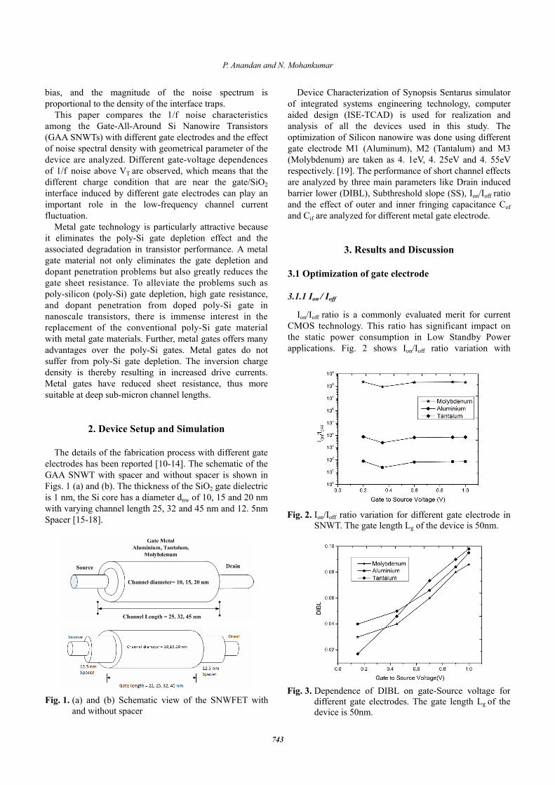
2. Device Setup and Simulation The details of the fabrication process with different gate
electrodes has been reported [10-14]. The schematic of the GAA SNWT with spacer and without spacer is shown in Figs. 1 (a) and (b). The thickness of the SiO2 gate dielectric is 1 nm, the Si core has a diameter dnw of 10, 15 and 20 nm with varying channel length 25, 32 and 45 nm and 12. 5nm Spacer [15-18].
Device Characterization of Synopsis Sentarus simulator of integrated systems engineering technology, computer aided design (ISE-TCAD) is used for realization and analysis of all the devices used in this study. The optimization of Silicon nanowire was done using different gate electrode M1 (Aluminum), M2 (Tantalum) and M3 (Molybdenum) are taken as 4. 1eV, 4. 25eV and 4. 55eV respectively. [19]. The performance of short channel effects are analyzed by three main parameters like Drain induced barrier lower (DIBL), Subthreshold slope (SS), Ion/Ioff ratio and the effect of outer and inner fringing capacitance Cof and Cif are analyzed for different metal gate electrode.
3. Results and Discussion
3.1 Optimization of gate electrode
3.1.1 Ion / Ioff Ion/Ioff ratio is a commonly evaluated merit for current
CMOS technology. This ratio has significant impact on the static power consumption in Low Standby Power applications. Fig. 2 shows Ion/Ioff ratio variation with
Fig. 1. (a) and (b) Schematic view of the SNWFET with
and without spacer
Fig. 2. Ion/Ioff ratio variation for different gate electrode in
SNWT. The gate length Lg of the device is 50nm.
Fig. 3. Dependence of DIBL on gate-Source voltage for
different gate electrodes. The gate length Lg of the device is 50nm.
Optimization and Characterization Of Gate Electrode Dependent Flicker Noise in Silicon Nanowire Transistors
744
different gate electrode From this graph, it is clear that SNWT with Molybdenum gate electrode shows higher Ion/Ioff ratio compared to tantalum and alumunium.
3.1.2 DIBL
The Important parameter describing the electrostatic
integrity of MOSFETs device performance is Drain Induced Barrier Lowering (DIBL) and is expressed as the shift of threshold voltage due to change in the drain voltage. DIBL for various gate electrodes is shown in Fig. 3 as a function of gate-source voltage. Molybdenum gate electrode based SNWT showed low DIBL value compared to tantalum and alumunium.
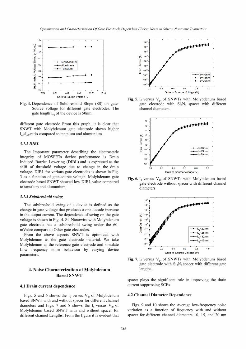
3.1.3 Subthreshold swing
The subthreshold swing of a device is defined as the
change in gate voltage that produces a one decade increase in the output current. The dependence of swing on the gate voltage is shown in Fig. 4. Si -Nanowire with Molybdenum gate electrode has a subthreshold swing under the 60-mV/dec compare to Other gate electrodes.
From the above aspects SNWT is optimized with Molybdenum as the gate electrode material. We take Molybdenum as the reference gate electrode and simulate Low frequency noise behaviour by varying device parameters.
4. Noise Characterization of Molybdenum Based SNWT
4.1 Drain current dependence
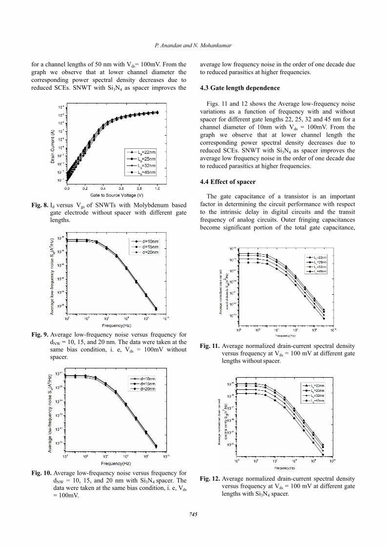
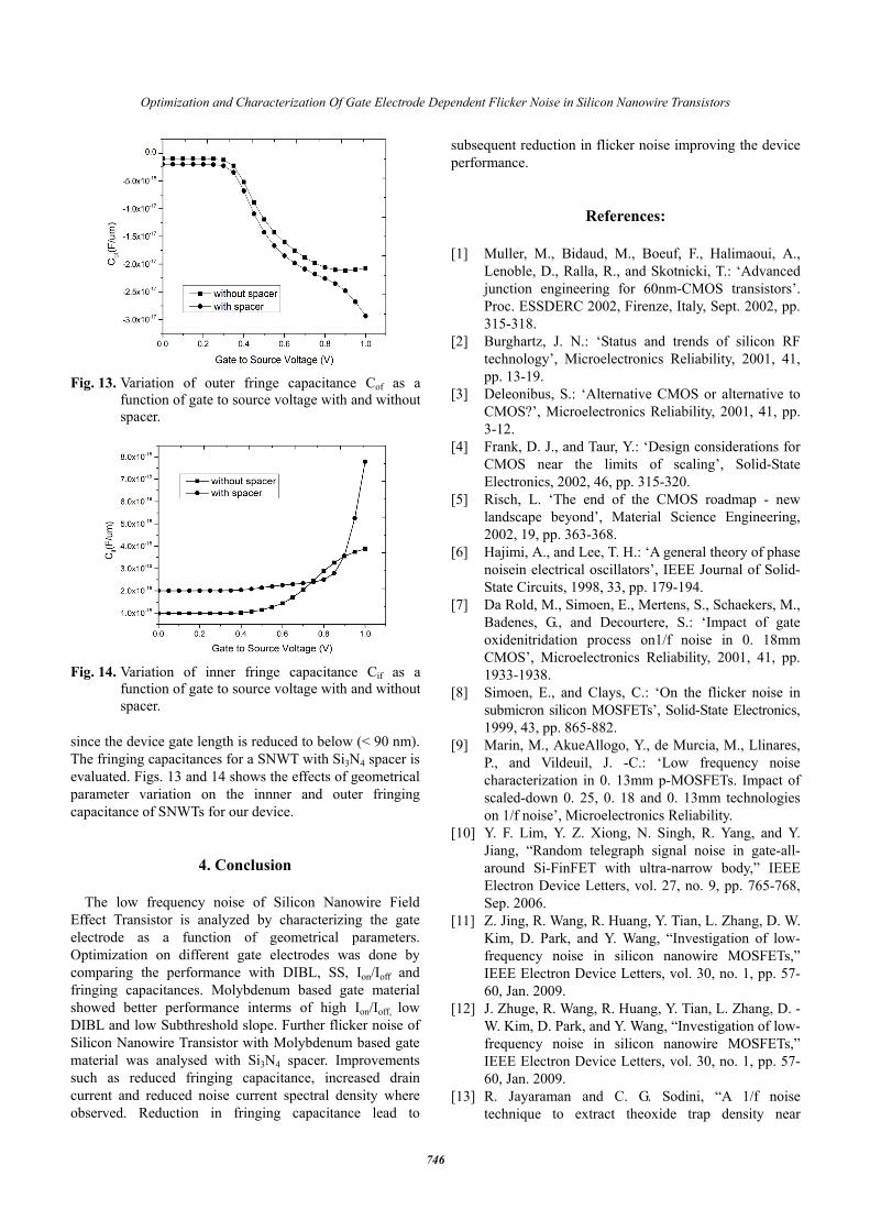
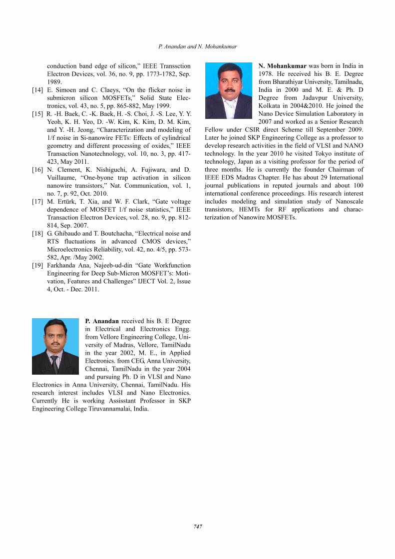
Figs. 5 and 6 shows the Id versus Vgs of Molybdenum
based SNWT with and without spacer for different channel diameters and Figs. 7 and 8 shows the Id versus Vgs of Molybdenum based SNWT with and without spacer for different channel Lengths. From the figure it is evident that
spacer plays the significant role in improving the drain current suppressing SCEs.
4.2 Channel Diameter Dependence
Figs. 9 and 10 shows the Average low-frequency noise
variation as a function of frequency with and without spacer for different channel diameters 10, 15, and 20 nm
Fig. 4. Dependence of Subthreshold Slope (SS) on gate-
Source voltage for different gate electrodes. The gate length Lg of the device is 50nm.
Fig. 5. Id versus Vgs of SNWTs with Molybdenum based
gate electrode with Si3N4 spacer with different channel diameters.
Fig. 6. Id versus Vgs of SNWTs with Molybdenum based
gate electrode without spacer with different channel diameters.
Fig. 7. Id versus Vgs of SNWTs with Molybdenum based
gate electrode with Si3N4 spacer with different gate lengths.
P. Anandan and N. Mohankumar
745
for a channel lengths of 50 nm with Vds= 100mV. From the graph we observe that at lower channel diameter the corresponding power spectral density decreases due to reduced SCEs. SNWT with Si3N4 as spacer improves the
average low frequency noise in the order of one decade due to reduced parasitics at higher frequencies.
4.3 Gate length dependence
Figs. 11 and 12 shows the Average low-frequency noise
variations as a function of frequency with and without spacer for different gate lengths 22, 25, 32 and 45 nm for a channel diameter of 10nm with Vds = 100mV. From the graph we observe that at lower channel length the corresponding power spectral density decreases due to reduced SCEs. SNWT with Si3N4 as spacer improves the average low frequency noise in the order of one decade due to reduced parasitics at higher frequencies.
4.4 Effect of spacer
The gate capacitance of a transistor is an important
factor in determining the circuit performance with respect to the intrinsic delay in digital circuits and the transit frequency of analog circuits. Outer fringing capacitances become significant portion of the total gate capacitance,
Fig. 8. Id versus Vgs of SNWTs with Molybdenum based
gate electrode without spacer with different gate lengths.
Fig. 9. Average low-frequency noise versus frequency for
dNW = 10, 15, and 20 nm. The data were taken at the same bias condition, i. e, Vds = 100mV withoutspacer.
Fig. 10. Average low-frequency noise versus frequency for
dNW = 10, 15, and 20 nm with Si3N4 spacer. The data were taken at the same bias condition, i. e, Vds= 100mV.
Fig. 11. Average normalized drain-current spectral density
versus frequency at Vds = 100 mV at different gate lengths without spacer.
Fig. 12. Average normalized drain-current spectral density
versus frequency at Vds = 100 mV at different gate lengths with Si3N4 spacer.
Optimization and Characterization Of Gate Electrode Dependent Flicker Noise in Silicon Nanowire Transistors
746
since the device gate length is reduced to below (< 90 nm). The fringing capacitances for a SNWT with Si3N4 spacer is evaluated. Figs. 13 and 14 shows the effects of geometrical parameter variation on the innner and outer fringing capacitance of SNWTs for our device.
4. Conclusion The low frequency noise of Silicon Nanowire Field
Effect Transistor is analyzed by characterizing the gate electrode as a function of geometrical parameters. Optimization on different gate electrodes was done by comparing the performance with DIBL, SS, Ion/Ioff and fringing capacitances. Molybdenum based gate material showed better performance interms of high Ion/Ioff, low DIBL and low Subthreshold slope. Further flicker noise of Silicon Nanowire Transistor with Molybdenum based gate material was analysed with Si3N4 spacer. Improvements such as reduced fringing capacitance, increased drain current and reduced noise current spectral density where observed. Reduction in fringing capacitance lead to
subsequent reduction in flicker noise improving the device performance.
References:
[1] Muller, M., Bidaud, M., Boeuf, F., Halimaoui, A., Lenoble, D., Ralla, R., and Skotnicki, T.: ‘Advanced junction engineering for 60nm-CMOS transistors’. Proc. ESSDERC 2002, Firenze, Italy, Sept. 2002, pp. 315-318.
[2] Burghartz, J. N.: ‘Status and trends of silicon RF technology’, Microelectronics Reliability, 2001, 41, pp. 13-19.
[3] Deleonibus, S.: ‘Alternative CMOS or alternative to CMOS?’, Microelectronics Reliability, 2001, 41, pp. 3-12.
[4] Frank, D. J., and Taur, Y.: ‘Design considerations for CMOS near the limits of scaling’, Solid-State Electronics, 2002, 46, pp. 315-320.
[5] Risch, L. ‘The end of the CMOS roadmap - new landscape beyond’, Material Science Engineering, 2002, 19, pp. 363-368.
[6] Hajimi, A., and Lee, T. H.: ‘A general theory of phase noisein electrical oscillators’, IEEE Journal of Solid-State Circuits, 1998, 33, pp. 179-194.
[7] Da Rold, M., Simoen, E., Mertens, S., Schaekers, M., Badenes, G., and Decourtere, S.: ‘Impact of gate oxidenitridation process on1/f noise in 0. 18mm CMOS’, Microelectronics Reliability, 2001, 41, pp. 1933-1938.
[8] Simoen, E., and Clays, C.: ‘On the flicker noise in submicron silicon MOSFETs’, Solid-State Electronics, 1999, 43, pp. 865-882.
[9] Marin, M., AkueAllogo, Y., de Murcia, M., Llinares, P., and Vildeuil, J. -C.: ‘Low frequency noise characterization in 0. 13mm p-MOSFETs. Impact of scaled-down 0. 25, 0. 18 and 0. 13mm technologies on 1/f noise’, Microelectronics Reliability.
[10] Y. F. Lim, Y. Z. Xiong, N. Singh, R. Yang, and Y. Jiang, “Random telegraph signal noise in gate-all-around Si-FinFET with ultra-narrow body,” IEEE Electron Device Letters, vol. 27, no. 9, pp. 765-768, Sep. 2006.
[11] Z. Jing, R. Wang, R. Huang, Y. Tian, L. Zhang, D. W. Kim, D. Park, and Y. Wang, “Investigation of low-frequency noise in silicon nanowire MOSFETs,” IEEE Electron Device Letters, vol. 30, no. 1, pp. 57-60, Jan. 2009.
[12] J. Zhuge, R. Wang, R. Huang, Y. Tian, L. Zhang, D. -W. Kim, D. Park, and Y. Wang, “Investigation of low-frequency noise in silicon nanowire MOSFETs,” IEEE Electron Device Letters, vol. 30, no. 1, pp. 57-60, Jan. 2009.
[13] R. Jayaraman and C. G. Sodini, “A 1/f noise technique to extract theoxide trap density near
Fig. 13. Variation of outer fringe capacitance Cof as a
function of gate to source voltage with and withoutspacer.
Fig. 14. Variation of inner fringe capacitance Cif as a
function of gate to source voltage with and withoutspacer.
P. Anandan and N. Mohankumar
747
conduction band edge of silicon,” IEEE Transsction Electron Devices, vol. 36, no. 9, pp. 1773-1782, Sep. 1989.
[14] E. Simoen and C. Claeys, “On the flicker noise in submicron silicon MOSFETs,” Solid State Elec-tronics, vol. 43, no. 5, pp. 865-882, May 1999.
[15] R. -H. Baek, C. -K. Baek, H. -S. Choi, J. -S. Lee, Y. Y. Yeoh, K. H. Yeo, D. -W. Kim, K. Kim, D. M. Kim, and Y. -H. Jeong, “Characterization and modeling of 1/f noise in Si-nanowire FETs: Effects of cylindrical geometry and different processing of oxides,” IEEE Transaction Nanotechnology, vol. 10, no. 3, pp. 417-423, May 2011.
[16] N. Clement, K. Nishiguchi, A. Fujiwara, and D. Vuillaume, “One-byone trap activation in silicon nanowire transistors,” Nat. Communication, vol. 1, no. 7, p. 92, Oct. 2010.
[17] M. Ertürk, T. Xia, and W. F. Clark, “Gate voltage dependence of MOSFET 1/f noise statistics,” IEEE Transaction Electron Devices, vol. 28, no. 9, pp. 812- 814, Sep. 2007.
[18] G. Ghibaudo and T. Boutchacha, “Electrical noise and RTS fluctuations in advanced CMOS devices,” Microelectronics Reliability, vol. 42, no. 4/5, pp. 573-582, Apr. /May 2002.
[19] Farkhanda Ana, Najeeb-ud-din “Gate Workfunction Engineering for Deep Sub-Micron MOSFET’s: Moti-vation, Features and Challenges” IJECT Vol. 2, Issue 4, Oct. - Dec. 2011.
P. Anandan received his B. E Degree in Electrical and Electronics Engg. from Vellore Engineering College, Uni-versity of Madras, Vellore, TamilNadu in the year 2002, M. E., in Applied Electronics. from CEG, Anna University, Chennai, TamilNadu in the year 2004 and pursuing Ph. D in VLSI and Nano
Electronics in Anna University, Chennai, TamilNadu. His research interest includes VLSI and Nano Electronics. Currently He is working Assisstant Professor in SKP Engineering College Tiruvannamalai, India.
N. Mohankumar was born in India in 1978. He received his B. E. Degree from Bharathiyar University, Tamilnadu, India in 2000 and M. E. & Ph. D Degree from Jadavpur University, Kolkata in 2004&2010. He joined the Nano Device Simulation Laboratory in 2007 and worked as a Senior Research
Fellow under CSIR direct Scheme till September 2009. Later he joined SKP Engineering College as a professor to develop research activities in the field of VLSI and NANO technology. In the year 2010 he visited Tokyo institute of technology, Japan as a visiting professor for the period of three months. He is currently the founder Chairman of IEEE EDS Madras Chapter. He has about 29 International journal publications in reputed journals and about 100 international conference proceedings. His research interest includes modeling and simulation study of Nanoscale transistors, HEMTs for RF applications and charac-terization of Nanowire MOSFETs.