Embed Size (px)
Citation preview
REVIEW
Optical storage arrays: a perspective for future big datastorage
Min Gu, Xiangping Li* and Yaoyu Cao*
The advance of nanophotonics has provided a variety of avenues for light–matter interaction at the nanometer scale through the
enriched mechanisms for physical and chemical reactions induced by nanometer-confined optical probes in nanocomposite
materials. These emerging nanophotonic devices and materials have enabled researchers to develop disruptive methods of
tremendously increasing the storage capacity of current optical memory. In this paper, we present a review of the recent
advancements in nanophotonics-enabled optical storage techniques. Particularly, we offer our perspective of using them as optical
storage arrays for next-generation exabyte data centers.
Light: Science & Applications (2014) 3, e177; doi:10.1038/lsa.2014.58; published online 23 May 2014
Keywords: big data centers; optical data storage; optical storage arrays; super-resolution
INTRODUCTION
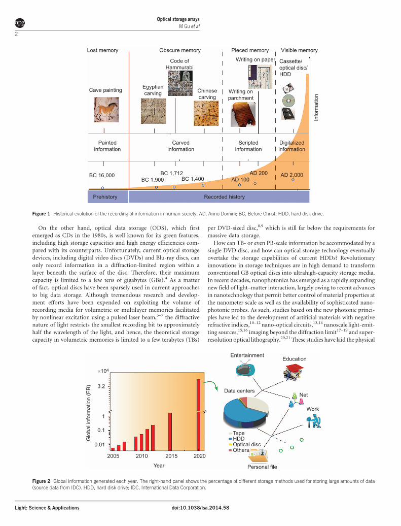
Historically, the recording and storage of information have undergone
a technological evolution from paintings to carvings, scribing and
digitization, as illustrated in Figure 1. The major revolution in this
developmental history is digitization, which allows music, sounds,
pictures, words and movies to be stored in a binary form. The inven-
tion of optical compact discs (CDs), where a laser beam was adopted to
store the binary data, was one of the major milestones in digital
information technology. Together with magnetic storage devices,
CDs have played a crucial role in the digital life of human beings.
Digital information technology has significantly boosted both
economies and societies. Therefore, the storage of information from
every sector, including education, entertainment, health, business
and so on, has already become an indispensable part of the many
activities of human beings in the information era. Consequently,
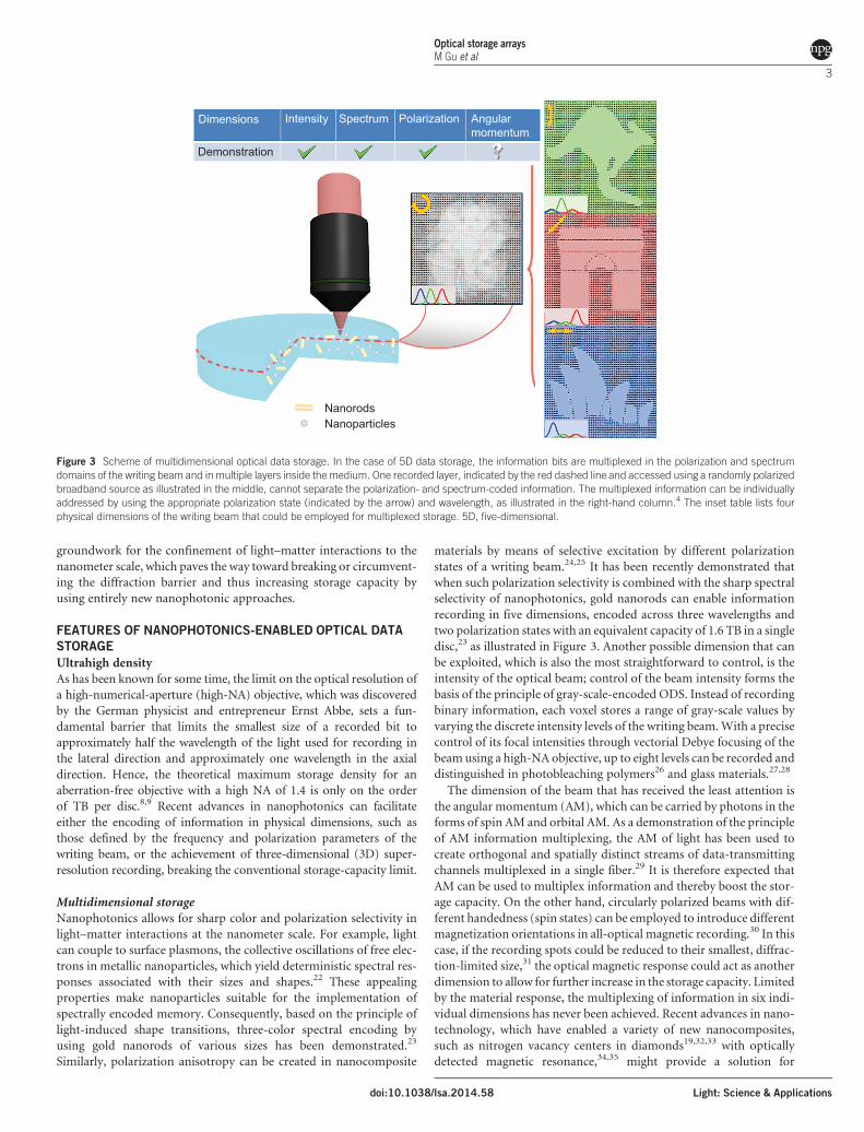
humans are entering an era of information explosion. It has been
estimated that the information generated by the major sectors is
nearly doubled each year. According to a report prepared by
International Data Corporation (IDC) in 2011, the total amount
of data generated globally will reach 35 ZB (1 ZB5103 EB5106
PB51012 GB) by 2020,1 as shown in Figure 2. Like the information
recorded in cave paintings, carvings and printings, the vast amount
of digital information that has been stored constitutes a core por-
tion of our civilization and history. However, there is a growing gap
between the amount of digital data being created and the extent of
available storage capacities. Big data centers with petabyte (PB) and
even exabyte (EB) capacities have emerged as the key enabling
techniques and core platforms for cloud computing and storage,
which have been heralded as the primary technical solution for the
next generation of big data storage.2,3 However, the infrastructure
of current information technology has been increasingly challenged
by the limited storage capacity of current digital media as well as
the shortcomings associated with the high energy consumption and
short lifetime of such media.
As shown in the right-hand panel of Figure 2, current methods of
data storage and archiving rely primarily on magnetization-based
storage technologies, such as hard disk drives (HDDs) and magnetic
tapes. To store vast amounts of information generated by clients, data
centers composed of arrays of thousands of HDDs have been built. The
sustainability of this technology is confronted by several crucial
problems. First, the capacity of HDD units, which is less than 1 TB
(1000 GB) per disk, is far below the requirements of next-generation
information storage. To increase the capacity to the PB scale, thou-
sands of HDD units must typically be assembled, which means that the
footprint of such a typical big data center is similar to that of a football
stadium in size. Second, HDD-based data centers are not energy effi-
cient. According to a statement issued by the US Environmental
Protection Agency, data centers in the US alone consumed a signifi-
cant amount of energy, accounting for 1.5% of the total US electricity
consumption in 2010 at a cost of $4.5 billion annually. Moreover, the
amount of energy consumption is expected to nearly double within
the next 5 years. Third, the limited lifetime of HDD technology
requires data migration every 2 or 3 years to avoid any data loss.
This significantly increases the energy-consumption burden, as a con-
siderable amount of energy is consumed during such data migration.
These challenges constitute fundamental obstacles to the longevity and
sustainability of current information technology. Accordingly, tech-
nologies with capacities greater than PBs, ultralow energy consump-
tion and ultralong lifetimes are in high demand to support big data
centers.
*These authors contributed equally to this paperCentre for Micro-Photonics, Faculty of Science, Engineering and Technology, Swinburne University of Technology, Hawthorn, VIC 3122, Australia
Correspondence: Professor M Gu, Centre for Micro-Photonics, Faculty of Science, Engineering and Technology, Swinburne University of Technology, Hawthorn, VIC 3122, AustraliaE-mail: [email protected]
Received 11 February 2014; revised 15 March 2014; accepted 23 March 2014
OPENLight: Science & Applications (2014) 3, e177; doi:10.1038/lsa.2014.58� 2014 CIOMP. All rights reserved 2047-7538/14
www.nature.com/lsa
On the other hand, optical data storage (ODS), which first
emerged as CDs in the 1980s, is well known for its green features,
including high storage capacities and high energy efficiencies com-
pared with its counterparts. Unfortunately, current optical storage
devices, including digital video discs (DVDs) and Blu-ray discs, can
only record information in a diffraction-limited region within a
layer beneath the surface of the disc. Therefore, their maximum
capacity is limited to a few tens of gigabytes (GBs).4 As a matter
of fact, optical discs have been sparsely used in current approaches
to big data storage. Although tremendous research and develop-
ment efforts have been expended on exploiting the volume of
recording media for volumetric or multilayer memories facilitated
by nonlinear excitation using a pulsed laser beam,5–7 the diffractive
nature of light restricts the smallest recording bit to approximately
half the wavelength of the light, and hence, the theoretical storage
capacity in volumetric memories is limited to a few terabytes (TBs)
per DVD-sized disc,8,9 which is still far below the requirements for
massive data storage.
How can TB- or even PB-scale information be accommodated by a
single DVD disc, and how can optical storage technology eventually
overtake the storage capabilities of current HDDs? Revolutionary
innovations in storage techniques are in high demand to transform
conventional GB optical discs into ultrahigh-capacity storage media.
In recent decades, nanophotonics has emerged as a rapidly expanding
new field of light–matter interaction, largely owing to recent advances
in nanotechnology that permit better control of material properties at
the nanometer scale as well as the availability of sophisticated nano-
photonic probes. As such, studies based on the new photonic princi-
ples have led to the development of artificial materials with negative
refractive indices,10–12 nano-optical circuits,13,14 nanoscale light-emit-
ting sources,15,16 imaging beyond the diffraction limit17–19 and super-
resolution optical lithography.20,21 These studies have laid the physical
×104
3.2
Glo
bal i
nfor
mat
ion
(EB
)
1
0.1
0.01
2005 2010 2015 2020
Personal file
Tape
Data centers
EntertainmentEducation
Net
Work
HDDOptical discOthers
Year
Figure 2 Global information generated each year. The right-hand panel shows the percentage of different storage methods used for storing large amounts of data
(source data from IDC). HDD, hard disk drive; IDC, International Data Corporation.
Cave painting
Lost memory Obscure memory Pieced memory Visible memory
Paintedinformation
Carvedinformation
Egyptiancarving Chinese
carvingWriting onparchment
Code ofHammurabi
Writing on paper
Info
rmat
ion
Cassette/optical disc/HDD
Scriptedinformation
Digitalizedinformation
BC 16,000 BC 1,712BC 1,900 BC 1,400
AD 200AD 100
AD 2,000
Prehistory Recorded history
Figure 1 Historical evolution of the recording of information in human society. AD, Anno Domini; BC, Before Christ; HDD, hard disk drive.
Optical storage arrays
M Gu et al
2
Light: Science & Applications doi:10.1038/lsa.2014.58
groundwork for the confinement of light–matter interactions to the
nanometer scale, which paves the way toward breaking or circumvent-
ing the diffraction barrier and thus increasing storage capacity by
using entirely new nanophotonic approaches.
FEATURES OF NANOPHOTONICS-ENABLED OPTICAL DATA
STORAGE
Ultrahigh density
As has been known for some time, the limit on the optical resolution of
a high-numerical-aperture (high-NA) objective, which was discovered
by the German physicist and entrepreneur Ernst Abbe, sets a fun-
damental barrier that limits the smallest size of a recorded bit to
approximately half the wavelength of the light used for recording in
the lateral direction and approximately one wavelength in the axial
direction. Hence, the theoretical maximum storage density for an
aberration-free objective with a high NA of 1.4 is only on the order
of TB per disc.8,9 Recent advances in nanophotonics can facilitate
either the encoding of information in physical dimensions, such as
those defined by the frequency and polarization parameters of the
writing beam, or the achievement of three-dimensional (3D) super-
resolution recording, breaking the conventional storage-capacity limit.
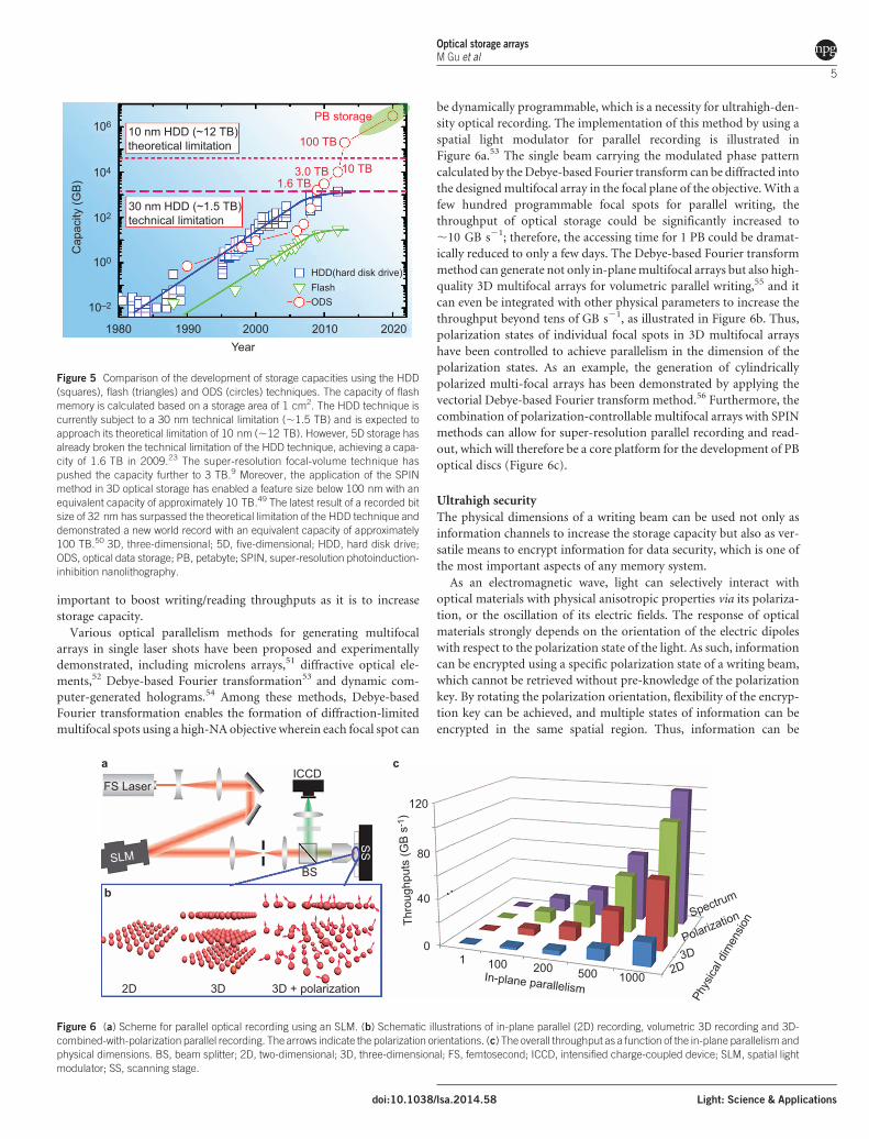
Multidimensional storageNanophotonics allows for sharp color and polarization selectivity in
light–matter interactions at the nanometer scale. For example, light
can couple to surface plasmons, the collective oscillations of free elec-
trons in metallic nanoparticles, which yield deterministic spectral res-
ponses associated with their sizes and shapes.22 These appealing
properties make nanoparticles suitable for the implementation of
spectrally encoded memory. Consequently, based on the principle of
light-induced shape transitions, three-color spectral encoding by
using gold nanorods of various sizes has been demonstrated.23
Similarly, polarization anisotropy can be created in nanocomposite
materials by means of selective excitation by different polarization
states of a writing beam.24,25 It has been recently demonstrated that
when such polarization selectivity is combined with the sharp spectral
selectivity of nanophotonics, gold nanorods can enable information
recording in five dimensions, encoded across three wavelengths and
two polarization states with an equivalent capacity of 1.6 TB in a single
disc,23 as illustrated in Figure 3. Another possible dimension that can
be exploited, which is also the most straightforward to control, is the
intensity of the optical beam; control of the beam intensity forms the
basis of the principle of gray-scale-encoded ODS. Instead of recording
binary information, each voxel stores a range of gray-scale values by
varying the discrete intensity levels of the writing beam. With a precise
control of its focal intensities through vectorial Debye focusing of the
beam using a high-NA objective, up to eight levels can be recorded and
distinguished in photobleaching polymers26 and glass materials.27,28
The dimension of the beam that has received the least attention is
the angular momentum (AM), which can be carried by photons in the
forms of spin AM and orbital AM. As a demonstration of the principle
of AM information multiplexing, the AM of light has been used to
create orthogonal and spatially distinct streams of data-transmitting
channels multiplexed in a single fiber.29 It is therefore expected that
AM can be used to multiplex information and thereby boost the stor-
age capacity. On the other hand, circularly polarized beams with dif-
ferent handedness (spin states) can be employed to introduce different
magnetization orientations in all-optical magnetic recording.30 In this
case, if the recording spots could be reduced to their smallest, diffrac-
tion-limited size,31 the optical magnetic response could act as another
dimension to allow for further increase in the storage capacity. Limited
by the material response, the multiplexing of information in six indi-
vidual dimensions has never been achieved. Recent advances in nano-
technology, which have enabled a variety of new nanocomposites,
such as nitrogen vacancy centers in diamonds19,32,33 with optically
detected magnetic resonance,34,35 might provide a solution for
Demonstration
Dimensions Intensity Spectrum Polarization Angularmomentum
NanorodsNanoparticles
Figure 3 Scheme of multidimensional optical data storage. In the case of 5D data storage, the information bits are multiplexed in the polarization and spectrum
domains of the writing beam and in multiple layers inside the medium. One recorded layer, indicated by the red dashed line and accessed using a randomly polarized
broadband source as illustrated in the middle, cannot separate the polarization- and spectrum-coded information. The multiplexed information can be individually
addressed by using the appropriate polarization state (indicated by the arrow) and wavelength, as illustrated in the right-hand column.4 The inset table lists four
physical dimensions of the writing beam that could be employed for multiplexed storage. 5D, five-dimensional.
Optical storage arraysM Gu et al
3
doi:10.1038/lsa.2014.58 Light: Science & Applications

exploiting the maximal number of information channels by simulta-
neously employing all physical dimensions of the writing beam.
3D super-resolution recording
A variety of methods have been proposed and demonstrated to break
the diffraction barrier in the near-field region and achieve super-
resolved areal memories.36,37 However, these approaches do not
exhibit the ability to record information in the volume of a medium.
Recently, inspired by a diffraction-unlimited far-field imaging
approach,38 scientists have developed super-resolution photoinduc-
tion-inhibition nanolithography (SPIN), which can break the diffrac-
tion barrier and achieve 3D super-resolved writing.
In contrast to conventional optical memory, SPIN is achieved by
employing dual beams during recording; the behavior of each beam is
still governed by its diffraction. In general, the two beams operate at
different frequencies enduing different functions, as illustrated in the
insets of Figure 4. One of the two beams, with a Gaussian shape, falls
within the transition bands of the materials and thus is responsible for
photoinduction. The other beam, with a spatially modulated intensity
distribution that is usually a doughnut shape (with zero light intensity
in the center), is responsible for inhibiting photoinduction everywhere
in the focal region except at its center. Consequently, the effective focal
spot can be made much smaller than the diffraction barrier by the
spatial superposition of the two beams and varying the intensity ratio
between the two beams.
By employing the principle of SPIN, researchers have successfully
demonstrated super-resolved line fabrication as well as dot recording
in a variety of photoinduction systems, as schematically illustrated in
the right-hand panel of insets in Figure 4. Table 1 summarizes the state
of the art of SPIN-based super-resolution recording methods for the
production of ultrafine features. In general, photoinduction can refer
to any photoinduced chemical or physical processes that initiate a
change in material properties, such as photochromism,39 photopoly-
merization20 and photoreduction,48 and that can also be terminated by
an inhibition beam operating at a different wavelength. As such, the
photochromism process has been used to inhibit photoabsorption, and
the smallest line-feature size of 30 nm (approximately one-tenth of the
wavelength l) has been successfully demonstrated.39 Recently, a photo-
polymerizable material with improved photosensitivity and mech-
anical stability has been developed and successfully applied in using
the SPIN method for the fabrication of suspended lines with the smal-
lest feature size down to 9 nm, or l/42.20 These exceptional features
open a new avenue toward diffraction-unlimited laser fabrication, as
well as for the development of ultrahigh-density optical memory.
The development of 3D super-resolved writing methods will enable
further decrease in the effective size of recorded bits to below 50 nm
and will eventually boost disc capacity to approach or even surpass the
PB scale in the near future, as projected in Figure 5. In the meantime,
sophisticated techniques for light manipulation on the focal plane are
necessary to maintain an effective focal spot smaller than the diffrac-
tion limit with enriched physical dimensions. The combination of
super-resolution techniques and multiplexing in the physical dimen-
sions can further expand disc storage capacity beyond hundreds of
PBs. Clearly, nanophotonics-enabled storage techniques are far super-
ior to the current HDD and flash memory techniques, which are
encountering density bottlenecks (Figure 5).
Ultrahigh throughputs
Another challenge confronting big data storage is low writing and
reading throughputs. Based on the current throughput (,20 MB s21)
of Blu-ray discs, it might take more than one and a half years to access
1 PB of information.3 Even taking the current HDD technique into
consideration (,100 MB s21), it would still require more than 100
days to access such a massive amount of data. Therefore, it is equally as
10000 Photo-induction
Effectivefocal spot
Photon-inhibition
Directlaser
recording/lithography
Super-resolution
Cap
acity
(TB
per
dis
c) 1000
100
10
10 50 100 150 200
Feature size (nm)
250 300
Figure 4 Projection of the maximal capacity that a single disc can hold as a
function of the feature size of the recorded bits. In the projection, the lateral
separation and the axial separation are set to 2.5 times and 8 times the feature
size, respectively. The insets illustrate the principle underlying SPIN’s ability to
break the diffraction barrier and achieve super-resolution recording/lithography.
Top inset: comparison of direct laser recording and super-resolution recording by
using SPIN methods. Bottom inset: comparison of conventional laser lithography
and super-resolution lithography. SPIN, super-resolution photoinduction-inhibi-
tion nanolithography.
Table 1 The development of SPIN methods
Photoinhibition methods Wavelength of photoinduction (nm) Wavelength of photoinhibition (nm) Lateral feature size (nm) Pattern
Photodeactivation21 800 800 ,100 (Fl) Dots
Photochromism39 325 633 30 (1/10l) Lines
Photoradical40 473 364 64 (Fl) Dots
Photoluminescence41 800 532 65 (1/12l) Lines
Photoradical42 488 375 40 (1/12l) Dots
Photodeactivation43 800 800 ,150 (Nl) Lines
Photoluminescence44 800 532 ,120 (1/7l) Lines
Photoabsorption45 800 642 ,120 (1/7l) Dots
Stimulated emission depletion46 780 532 55 (1/14l) Lines
Photoradical20 800 375 9 (1/42l) Lines
Photoswitching47 405 491 200 (resolution) Dots
*SPIN, super-resolution photoinduction-inhibition nanolithography.
Optical storage arrays
M Gu et al
4
Light: Science & Applications doi:10.1038/lsa.2014.58
important to boost writing/reading throughputs as it is to increase
storage capacity.
Various optical parallelism methods for generating multifocal
arrays in single laser shots have been proposed and experimentally
demonstrated, including microlens arrays,51 diffractive optical ele-
ments,52 Debye-based Fourier transformation53 and dynamic com-
puter-generated holograms.54 Among these methods, Debye-based
Fourier transformation enables the formation of diffraction-limited
multifocal spots using a high-NA objective wherein each focal spot can
be dynamically programmable, which is a necessity for ultrahigh-den-
sity optical recording. The implementation of this method by using a
spatial light modulator for parallel recording is illustrated in
Figure 6a.53 The single beam carrying the modulated phase pattern
calculated by the Debye-based Fourier transform can be diffracted into
the designed multifocal array in the focal plane of the objective. With a
few hundred programmable focal spots for parallel writing, the
throughput of optical storage could be significantly increased to
,10 GB s21; therefore, the accessing time for 1 PB could be dramat-
ically reduced to only a few days. The Debye-based Fourier transform
method can generate not only in-plane multifocal arrays but also high-
quality 3D multifocal arrays for volumetric parallel writing,55 and it
can even be integrated with other physical parameters to increase the
throughput beyond tens of GB s21, as illustrated in Figure 6b. Thus,
polarization states of individual focal spots in 3D multifocal arrays
have been controlled to achieve parallelism in the dimension of the
polarization states. As an example, the generation of cylindrically
polarized multi-focal arrays has been demonstrated by applying the
vectorial Debye-based Fourier transform method.56 Furthermore, the
combination of polarization-controllable multifocal arrays with SPIN
methods can allow for super-resolution parallel recording and read-
out, which will therefore be a core platform for the development of PB
optical discs (Figure 6c).
Ultrahigh security
The physical dimensions of a writing beam can be used not only as
information channels to increase the storage capacity but also as ver-
satile means to encrypt information for data security, which is one of
the most important aspects of any memory system.
As an electromagnetic wave, light can selectively interact with
optical materials with physical anisotropic properties via its polariza-
tion, or the oscillation of its electric fields. The response of optical
materials strongly depends on the orientation of the electric dipoles
with respect to the polarization state of the light. As such, information
can be encrypted using a specific polarization state of a writing beam,
which cannot be retrieved without pre-knowledge of the polarization
key. By rotating the polarization orientation, flexibility of the encryp-
tion key can be achieved, and multiple states of information can be
encrypted in the same spatial region. Thus, information can be
106
Cap
acity
(GB
)
104
102
100
10–2
1980 1990 2000
10 nm HDD (~12 TB)theoretical limitation
30 nm HDD (~1.5 TB)technical limitation
2010
HDD(hard disk drive)
PB storage
100 TB
10 TB3.0 TB1.6 TB
FlashODS
2020Year
Figure 5 Comparison of the development of storage capacities using the HDD
(squares), flash (triangles) and ODS (circles) techniques. The capacity of flash
memory is calculated based on a storage area of 1 cm2. The HDD technique is
currently subject to a 30 nm technical limitation (,1.5 TB) and is expected to
approach its theoretical limitation of 10 nm (,12 TB). However, 5D storage has
already broken the technical limitation of the HDD technique, achieving a capa-
city of 1.6 TB in 2009.23 The super-resolution focal-volume technique has
pushed the capacity further to 3 TB.9 Moreover, the application of the SPIN
method in 3D optical storage has enabled a feature size below 100 nm with an
equivalent capacity of approximately 10 TB.49 The latest result of a recorded bit
size of 32 nm has surpassed the theoretical limitation of the HDD technique and
demonstrated a new world record with an equivalent capacity of approximately
100 TB.50 3D, three-dimensional; 5D, five-dimensional; HDD, hard disk drive;
ODS, optical data storage; PB, petabyte; SPIN, super-resolution photoinduction-
inhibition nanolithography.
a
FS Laser
SLM
ICCD
120
80
40
01 100 200 500 1000 2D
Thro
ughp
uts
(GB
s-1
)
3D
Phys
ical d
imen
sion
PolarizationSpectrum
In-plane parallelism2D 3D 3D + polarization
BS
SS
b
c
Figure 6 (a) Scheme for parallel optical recording using an SLM. (b) Schematic illustrations of in-plane parallel (2D) recording, volumetric 3D recording and 3D-
combined-with-polarization parallel recording. The arrows indicate the polarization orientations. (c) The overall throughput as a function of the in-plane parallelism and
physical dimensions. BS, beam splitter; 2D, two-dimensional; 3D, three-dimensional; FS, femtosecond; ICCD, intensified charge-coupled device; SLM, spatial light
modulator; SS, scanning stage.
Optical storage arraysM Gu et al
5
doi:10.1038/lsa.2014.58 Light: Science & Applications
encrypted in the two polarization states of writing beams at 06- and 456-
oriented polarizations through polarization-induced birefringence.24
Recently, it has been demonstrated that by employing the depolariza-
tion effect through the tight focusing of a radially polarized beam,
one can generate a longitudinal polarization state within the focal
region.57,58 Through the superposition of weighted radially and
azimuthally polarized beams, a 3D arbitrary polarization orienta-
tion can be achieved in the focal region of a high-NA objective. In
combination with the sharp polarization sensitivity of gold nanor-
ods, 3D polarization encryption within a solid angle in the focal
plane has been demonstrated for ultrahigh security,59 as illustrated
in Figure 7a.
Additionally, the enrichment of the physical dimensions for light–
matter interactions offered by nanophotonic approaches enables
information to be recorded in multimode material responses, which
opens a new avenue toward a high level of information security. For
example, simultaneous changes in the refractive index and fluorescence
intensity of graphene-based materials have been demonstrated to hold
the potential for hologram-encoded multimode recording,61 as shown in
Figure 7b. On the one hand, the information can be randomly accessed
through two-photon fluorescence readout. On the other hand, the
information can be simultaneously encrypted in holograms, ensuring
its integrity and durability. It is possible to integrate hologram-encrypted
multimode recording with other physical dimensions, such as polariza-
tion and AM, to achieve an even higher level of information security, as
illustrated in Figure 7c. However, the experimental achievement of such
a high level of security strongly depends on material properties of the
recording medium, specifically, its deterministic responses to light with
various characteristics. Nanotechnology that offers the ability to engineer
and control material properties on the nanoscale may provide a solid
platform for future ultrahigh-security optical storage.
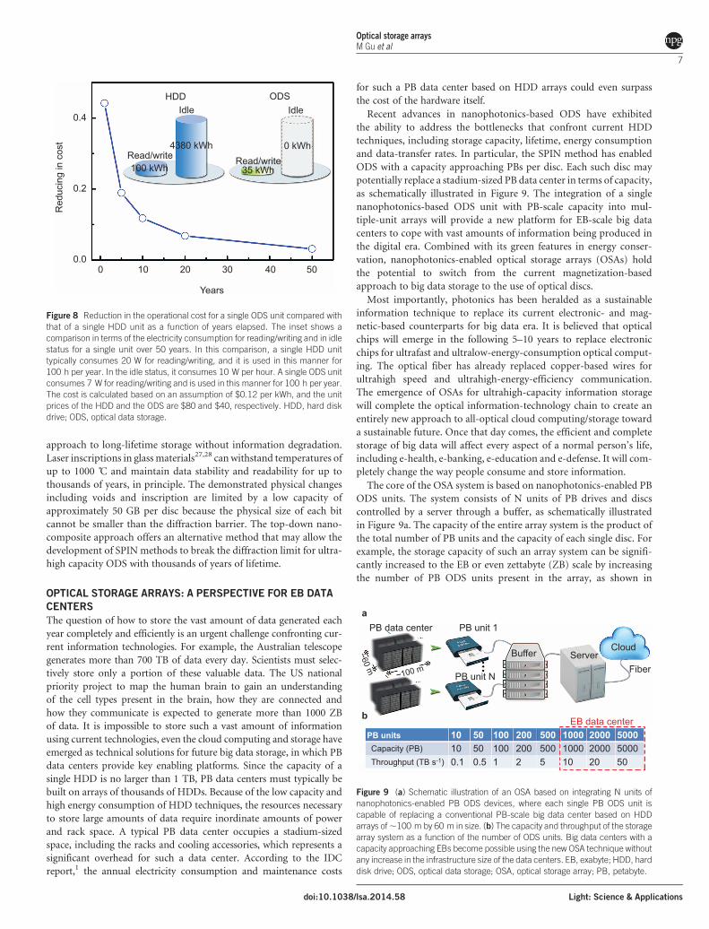
Ultralong lifetime
As we have noted, magnetization-based HDD techniques have a lim-
ited lifetime of 2–5 years, and therefore, frequent data migration is
needed to avoid potential data loss. However, ODS has a longer life-
time than HDDs, which dramatically reduces the required frequency
of data migration. In addition, ODS only consumes energy when the
data are written or read out and does not consume any energy when
the optical disc is in idle state. For comparison, Figure 8 illustrates the
power consumption and operational cost of information storage
incurred by a single HDD (4480 kWh) and a single disc (35 kWh)
over 50 years. Clearly, optical technology greatly reduces the waste
generated by frequent data migration, reduces the energy consump-
tion in idle status and reduces the cost for the replacement of new units
associated with short lifetimes. Moreover, increasing the lifetime of
ODS to greater than 50 years can dramatically increase the savings in
overall expenditures, including electricity and costs for storage
devices, by more than 96% compared with HDD techniques.
Consequently, the development of ODS with ultralong lifetimes has
been a subject of intensive research. Permanent laser-induced physical
changes, such as voids in polymers62 and glass materials,63 provide an
a b
c 32
Ultr
a-se
curit
y le
vel 3
Leve
l 2Le
vel 1
Hologram-encodedmultimode recording
Multimode+ polarization
+ angular momentum
Multimode+ polarization
3D polarization
multimode recording2D polarization
Hologramencrypted
InformationencodingFS laser
z
x y
z
x y
z
x y
z
x y
θ=π/2
θ=π/14
θ=π/2
θ~0
β=π/3
β=0
β=0
β=0~2π
2P FL reading
Diffraction reading
24
Key
sta
tes
16
8
0
Figure 7 (a) Scheme for 3D polarization encryption using 3D oriented polarization states.60 (b) Illustration of hologram-encoded multimode recording for enhanced
data security. Information bits can be randomly accessed through the 2P fluorescence readout and retrieved in the diffraction mode of the recorded holograms.61
(c) Projection of levels of information security by combining multimode recording with other physical dimensions. 3D, three-dimensional; FL, fluorescence; FS,
femtosecond; 2P, two-photon.
Optical storage arrays
M Gu et al
6
Light: Science & Applications doi:10.1038/lsa.2014.58
approach to long-lifetime storage without information degradation.
Laser inscriptions in glass materials27,28 can withstand temperatures of
up to 1000 6C and maintain data stability and readability for up to
thousands of years, in principle. The demonstrated physical changes
including voids and inscription are limited by a low capacity of
approximately 50 GB per disc because the physical size of each bit
cannot be smaller than the diffraction barrier. The top-down nano-
composite approach offers an alternative method that may allow the
development of SPIN methods to break the diffraction limit for ultra-
high capacity ODS with thousands of years of lifetime.
OPTICAL STORAGE ARRAYS: A PERSPECTIVE FOR EB DATA
CENTERS
The question of how to store the vast amount of data generated each
year completely and efficiently is an urgent challenge confronting cur-
rent information technologies. For example, the Australian telescope
generates more than 700 TB of data every day. Scientists must selec-
tively store only a portion of these valuable data. The US national
priority project to map the human brain to gain an understanding
of the cell types present in the brain, how they are connected and
how they communicate is expected to generate more than 1000 ZB
of data. It is impossible to store such a vast amount of information
using current technologies, even the cloud computing and storage have
emerged as technical solutions for future big data storage, in which PB
data centers provide key enabling platforms. Since the capacity of a
single HDD is no larger than 1 TB, PB data centers must typically be
built on arrays of thousands of HDDs. Because of the low capacity and
high energy consumption of HDD techniques, the resources necessary
to store large amounts of data require inordinate amounts of power
and rack space. A typical PB data center occupies a stadium-sized
space, including the racks and cooling accessories, which represents a
significant overhead for such a data center. According to the IDC
report,1 the annual electricity consumption and maintenance costs
for such a PB data center based on HDD arrays could even surpass
the cost of the hardware itself.
Recent advances in nanophotonics-based ODS have exhibited
the ability to address the bottlenecks that confront current HDD
techniques, including storage capacity, lifetime, energy consumption
and data-transfer rates. In particular, the SPIN method has enabled
ODS with a capacity approaching PBs per disc. Each such disc may
potentially replace a stadium-sized PB data center in terms of capacity,
as schematically illustrated in Figure 9. The integration of a single
nanophotonics-based ODS unit with PB-scale capacity into mul-
tiple-unit arrays will provide a new platform for EB-scale big data
centers to cope with vast amounts of information being produced in
the digital era. Combined with its green features in energy conser-
vation, nanophotonics-enabled optical storage arrays (OSAs) hold
the potential to switch from the current magnetization-based
approach to big data storage to the use of optical discs.
Most importantly, photonics has been heralded as a sustainable
information technique to replace its current electronic- and mag-
netic-based counterparts for big data era. It is believed that optical
chips will emerge in the following 5–10 years to replace electronic
chips for ultrafast and ultralow-energy-consumption optical comput-
ing. The optical fiber has already replaced copper-based wires for
ultrahigh speed and ultrahigh-energy-efficiency communication.
The emergence of OSAs for ultrahigh-capacity information storage
will complete the optical information-technology chain to create an
entirely new approach to all-optical cloud computing/storage toward
a sustainable future. Once that day comes, the efficient and complete
storage of big data will affect every aspect of a normal person’s life,
including e-health, e-banking, e-education and e-defense. It will com-
pletely change the way people consume and store information.
The core of the OSA system is based on nanophotonics-enabled PB
ODS units. The system consists of N units of PB drives and discs
controlled by a server through a buffer, as schematically illustrated
in Figure 9a. The capacity of the entire array system is the product of
the total number of PB units and the capacity of each single disc. For
example, the storage capacity of such an array system can be signifi-
cantly increased to the EB or even zettabyte (ZB) scale by increasing
the number of PB ODS units present in the array, as shown in
0.4
Red
ucin
g in
cos
t
0.2
0.00 10 20 30
Years
Read/write100 kWh
HDDIdle
4380 kWhRead/write
35 kWh
0 kWh
IdleODS
40 50
Figure 8 Reduction in the operational cost for a single ODS unit compared with
that of a single HDD unit as a function of years elapsed. The inset shows a
comparison in terms of the electricity consumption for reading/writing and in idle
status for a single unit over 50 years. In this comparison, a single HDD unit
typically consumes 20 W for reading/writing, and it is used in this manner for
100 h per year. In the idle status, it consumes 10 W per hour. A single ODS unit
consumes 7 W for reading/writing and is used in this manner for 100 h per year.
The cost is calculated based on an assumption of $0.12 per kWh, and the unit
prices of the HDD and the ODS are $80 and $40, respectively. HDD, hard disk
drive; ODS, optical data storage.
PB data centera
b
10 50 100 200 500 1000 2000 5000100.1 0.5 1 10 20 502 5
50 100 200 500 1000 2000 5000
PB unit 1
PB unit N
PB unitsCapacity (PB)Throughput (TB s-1)
Buffer ServerCloud
Fiber
EB data center
~100 m
~60 m
Figure 9 (a) Schematic illustration of an OSA based on integrating N units of
nanophotonics-enabled PB ODS devices, where each single PB ODS unit is
capable of replacing a conventional PB-scale big data center based on HDD
arrays of ,100 m by 60 m in size. (b) The capacity and throughput of the storage
array system as a function of the number of ODS units. Big data centers with a
capacity approaching EBs become possible using the new OSA technique without
any increase in the infrastructure size of the data centers. EB, exabyte; HDD, hard
disk drive; ODS, optical data storage; OSA, optical storage array; PB, petabyte.
Optical storage arraysM Gu et al
7
doi:10.1038/lsa.2014.58 Light: Science & Applications
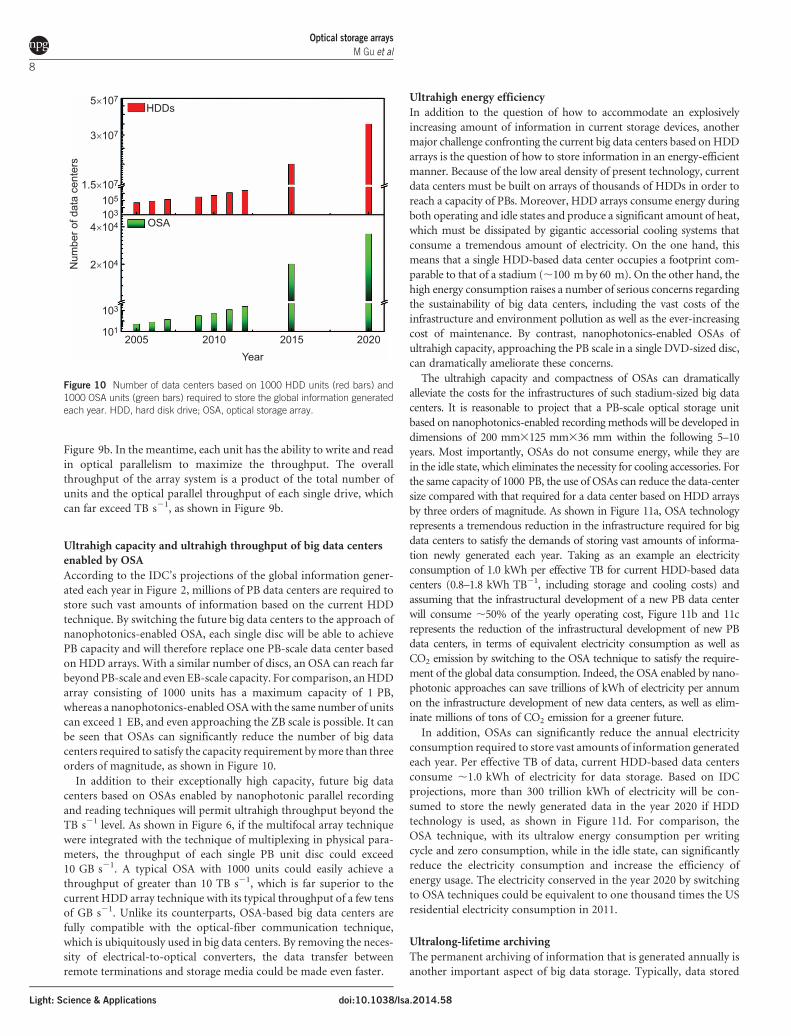
Figure 9b. In the meantime, each unit has the ability to write and read
in optical parallelism to maximize the throughput. The overall
throughput of the array system is a product of the total number of
units and the optical parallel throughput of each single drive, which
can far exceed TB s21, as shown in Figure 9b.
Ultrahigh capacity and ultrahigh throughput of big data centers
enabled by OSA
According to the IDC’s projections of the global information gener-
ated each year in Figure 2, millions of PB data centers are required to
store such vast amounts of information based on the current HDD
technique. By switching the future big data centers to the approach of
nanophotonics-enabled OSA, each single disc will be able to achieve
PB capacity and will therefore replace one PB-scale data center based
on HDD arrays. With a similar number of discs, an OSA can reach far
beyond PB-scale and even EB-scale capacity. For comparison, an HDD
array consisting of 1000 units has a maximum capacity of 1 PB,
whereas a nanophotonics-enabled OSA with the same number of units
can exceed 1 EB, and even approaching the ZB scale is possible. It can
be seen that OSAs can significantly reduce the number of big data
centers required to satisfy the capacity requirement by more than three
orders of magnitude, as shown in Figure 10.
In addition to their exceptionally high capacity, future big data
centers based on OSAs enabled by nanophotonic parallel recording
and reading techniques will permit ultrahigh throughput beyond the
TB s21 level. As shown in Figure 6, if the multifocal array technique
were integrated with the technique of multiplexing in physical para-
meters, the throughput of each single PB unit disc could exceed
10 GB s21. A typical OSA with 1000 units could easily achieve a
throughput of greater than 10 TB s21, which is far superior to the
current HDD array technique with its typical throughput of a few tens
of GB s21. Unlike its counterparts, OSA-based big data centers are
fully compatible with the optical-fiber communication technique,
which is ubiquitously used in big data centers. By removing the neces-
sity of electrical-to-optical converters, the data transfer between
remote terminations and storage media could be made even faster.
Ultrahigh energy efficiency
In addition to the question of how to accommodate an explosively
increasing amount of information in current storage devices, another
major challenge confronting the current big data centers based on HDD
arrays is the question of how to store information in an energy-efficient
manner. Because of the low areal density of present technology, current
data centers must be built on arrays of thousands of HDDs in order to
reach a capacity of PBs. Moreover, HDD arrays consume energy during
both operating and idle states and produce a significant amount of heat,
which must be dissipated by gigantic accessorial cooling systems that
consume a tremendous amount of electricity. On the one hand, this
means that a single HDD-based data center occupies a footprint com-
parable to that of a stadium (,100 m by 60 m). On the other hand, the
high energy consumption raises a number of serious concerns regarding
the sustainability of big data centers, including the vast costs of the
infrastructure and environment pollution as well as the ever-increasing
cost of maintenance. By contrast, nanophotonics-enabled OSAs of
ultrahigh capacity, approaching the PB scale in a single DVD-sized disc,
can dramatically ameliorate these concerns.
The ultrahigh capacity and compactness of OSAs can dramatically
alleviate the costs for the infrastructures of such stadium-sized big data
centers. It is reasonable to project that a PB-scale optical storage unit
based on nanophotonics-enabled recording methods will be developed in
dimensions of 200 mm3125 mm336 mm within the following 5–10
years. Most importantly, OSAs do not consume energy, while they are
in the idle state, which eliminates the necessity for cooling accessories. For
the same capacity of 1000 PB, the use of OSAs can reduce the data-center
size compared with that required for a data center based on HDD arrays
by three orders of magnitude. As shown in Figure 11a, OSA technology
represents a tremendous reduction in the infrastructure required for big
data centers to satisfy the demands of storing vast amounts of informa-
tion newly generated each year. Taking as an example an electricity
consumption of 1.0 kWh per effective TB for current HDD-based data
centers (0.8–1.8 kWh TB21, including storage and cooling costs) and
assuming that the infrastructural development of a new PB data center
will consume ,50% of the yearly operating cost, Figure 11b and 11c
represents the reduction of the infrastructural development of new PB
data centers, in terms of equivalent electricity consumption as well as
CO2 emission by switching to the OSA technique to satisfy the require-
ment of the global data consumption. Indeed, the OSA enabled by nano-
photonic approaches can save trillions of kWh of electricity per annum
on the infrastructure development of new data centers, as well as elim-
inate millions of tons of CO2 emission for a greener future.
In addition, OSAs can significantly reduce the annual electricity
consumption required to store vast amounts of information generated
each year. Per effective TB of data, current HDD-based data centers
consume ,1.0 kWh of electricity for data storage. Based on IDC
projections, more than 300 trillion kWh of electricity will be con-
sumed to store the newly generated data in the year 2020 if HDD
technology is used, as shown in Figure 11d. For comparison, the
OSA technique, with its ultralow energy consumption per writing
cycle and zero consumption, while in the idle state, can significantly
reduce the electricity consumption and increase the efficiency of
energy usage. The electricity conserved in the year 2020 by switching
to OSA techniques could be equivalent to one thousand times the US
residential electricity consumption in 2011.
Ultralong-lifetime archiving
The permanent archiving of information that is generated annually is
another important aspect of big data storage. Typically, data stored
5×10⁷
OSA
HDDs
2005 2010Year
2015 2020
3×10⁷
Num
ber o
f dat
a ce
nter
s
4×10⁴
2×10⁴
1.5×10⁷
105
103
103
101
Figure 10 Number of data centers based on 1000 HDD units (red bars) and
1000 OSA units (green bars) required to store the global information generated
each year. HDD, hard disk drive; OSA, optical storage array.
Optical storage arrays
M Gu et al
8
Light: Science & Applications doi:10.1038/lsa.2014.58
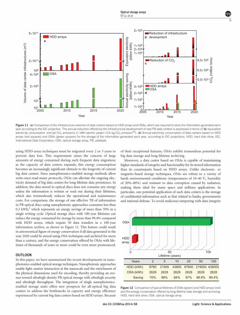
using HDD-array techniques must be migrated every 2 or 3 years to
prevent data loss. This requirement raises the concern of large
amounts of energy consumed during such frequent data migration;
as the capacity of data centers expands, this energy consumption
becomes an increasingly significant obstacle to the longevity of current
big data centers. Since nanophotonics-enabled storage methods allow
write-once-read-many protocols, OSAs can alleviate the ongoing elec-
tricity demand of big data centers for long-lifetime data persistence. In
addition, the data stored in optical discs does not consume any energy
unless the information is written or read out during their lifetimes,
which also tremendously reduces the operational and maintenance
costs. For comparison, the storage of one effective TB of information
in PB optical discs using nanophotonic approaches consumes less than
0.3 kWh,4 which represents an energy savings of more than 70% in a
single writing cycle. Optical storage discs with 100-year lifetimes can
reduce the energy consumed for storage by more than 99.4% compared
with HDD arrays, which require 50 data transfers in a 100-year
information archive, as shown in Figure 12. This feature could result
in astronomical figure of energy conservation if all data generated in the
year 2020 could be stored using OSA techniques and archived for more
than a century, and the energy conservation offered by OSAs with life-
times of thousands of years or more could be even more pronounced.
OUTLOOK
In this paper, we have summarized the recent developments in nano-
photonics-enabled optical storage techniques. Nanophotonic approaches
enable light–matter interaction at the nanoscale and the enrichment of
the physical dimensions used for encoding, thereby providing an ave-
nue toward ultrahigh-density PB optical storage with ultrahigh security
and ultrahigh throughput. The integration of single nanophotonics-
enabled storage units offers new prospects for all-optical big data
centers to address the bottlenecks in capacity and energy efficiency
experienced by current big data centers based on HDD arrays. Because
of their exceptional features, OSAs exhibit tremendous potential for
big data storage and long-lifetime archiving.
Moreover, a data center based on OSAs is capable of maintaining
higher standards of integrity and functionality for its stored information
than its counterparts based on HDD arrays. Unlike electronic- or
magnetic-based storage techniques, OSAs are robust to a variety of
harsh environmental conditions (temperatures of 10–40 6C, humidity
of 20%–80%) and resistant to data corruption caused by radiation,
making them ideal for many space and military applications. In
particular, one potential application of such data centers is the storage
of confidential information such as that related to banks, governments
and national defense. To avoid malicious tampering with data integrity
5×10¹¹
HDD arraysReduction of infrastructuredeveopment
Reduction of CO2
HDD arraysOSA
OSA
2005 2010 2015Year
2020 2005 2010 2015Year
2020
Volu
me
of d
ata
cent
er in
frast
ruct
ures
(m3 )
Equ
ival
ent e
lect
ricity
(bill
ion
kWh)
Ann
ual e
lect
ricity
sav
ing
(bill
ion
KW
h)
2×10⁵
9.0×10⁴
CO
2 (m
illio
n to
ns)
6.0×10⁴
5.0×10³
1×10⁵
3×10⁵
2×10⁵
1×10⁵
1×1040
1×1042×104
2×10¹¹
4×10⁴
2×10⁴
108
103
101
ab
c
d
Figure 11 (a) Comparison of the infrastructure volumes of data centers based on HDD arrays and OSAs, which are required to store the information generated each
year according to the IDC projection. The annual reduction offered by the infrastructural development of new PB data centers is expressed in terms of (b) equivalent
electricity consumption and (c) CO2 emissions (1 kWh electric power50.6 kg CO2 emission64). (d) Annual electricity consumption of data centers based on HDD
arrays (red squares) and OSAs (green squares) for the storage of the information generated each year, according to IDC projections. HDD, hard disk drive; IDC,
International Data Corporation; OSA, optical storage array; PB, petabyte.
OSA
HDDarray
0 50 100Lifetime (years)
Years
HDD (kWh)OSA (kWh)
Saving
2 5 10 20 50 100
43800087602628 2628 2628 2628 2628
21900 43800 87600 2190002628
99.4%98.8%97%94%88%70%
Figure 12 Comparison of typical lifetimes of OSAs (green) and HDD arrays (red)
and the energy conservation offered by long-lifetime data storage and archiving.
HDD, hard disk drive; OSA, optical storage array.
Optical storage arraysM Gu et al
9
doi:10.1038/lsa.2014.58 Light: Science & Applications
and breaches of information confidence, the enriched physical dimen-
sions of light provide exceptional protocols for the encryption informa-
tion in these physical parameters instead of the conventional binary
information storage offered by HDD techniques. This intriguing feature
of OSAs enables orders-of-magnitude-increased flexibility in the gen-
eration of encryption keys, opening a new avenue for information
storage with ultrahigh security. Moreover, OSAs allow for write-once-
read-many protocols in which information, once written, cannot be
modified. This type of write protection affords reliability in information
storage as well as the assurance that the data cannot be tampered with
once written to the storage device.
In addition, the cost for information storage can be reduced from
the current price of ,$1 per GB to well below $0.01 per GB by switch-
ing from HDDs to OSA techniques. Over the past two decades, ODS
has proven to be a great success in the entertainment sector, with a
global production of more than 2000 billion discs and a market size of
multiple billions of US dollars per annum. The proposed OSA, with its
exceptional capacity and energy efficiency, will become a key enabling
platform for the sustainability of our digital economy and society
powered by information technologies. It is reasonable to project that
OSAs will gain a tremendous share in the big data technologies in the
near future, with a global market on the scale of ,30 billion US dollars
per annum.65 Together with the booming optical chip and optical
fiber techniques, OSAs functioning as relay stations for data streams
or warehouses for information archiving will be able to promote a
brand-new paradigm of all-optical information management toward a
sustainable future for big data storage.
ACKNOWLEDGMENTSThe authors thank the Australian Research Council for its support through the
Laureate Fellowship project (FL100100099).
1 Gantz J, Reinsel D. The Digital Universe in 2020: Big Data, Bigger Digital Shadows,and Biggest Growth in the Far East. Framingham, MA: IDC; 2012. http://www.emc.com/leadership/digital-universe/index.htm.
2 Schadt EE, Linderman MD, Sorenson J, Lee L, Nolan GP. Computational solutions tolarge-scale data management and analysis. Nat Rev Genet 2010; 11, 647–657.
3 Trelles O, Prins P, Snir M, Jansen RC. Big data, but are we ready? Nat Rev Genet 2011;12: 224.
4 Gu M, Li X. The road to multi-dimensional bit-by-bit optical data storage. Optics &Photonics News 2010; 21: 28–33.
5 Parthenopoulos DA, Rentzepis PM. Three-dimensional optical storage memory.Science 1989; 245: 843–845.
6 Day D, Gu M, Smallridge A. Use of two-photon excitation for erasable-rewritable three-dimensional bit optical data storage in a photorefractive polymer. Opt Lett 1999; 24:948–950.
7 Kawata Y, Ishitobi H, Kawata S. Use of two-photon absorption in a photorefractivecrystal for three-dimensional optical memory. Opt Lett 1998; 23: 756–758.
8 Day D, Gu M. Effects of refractive-index mismatch on three-dimensional optical data-storage density in a two-photon bleaching polymer. Appl Opt 1998; 37: 6299–6304.
9 Li X, Cao Y, Gu M. Superresolution-focal-volume induced 3.0 Tbytes/disk capacity byfocusing a radially polarized beam. Opt Lett 2011; 36: 2510–2512.
10 Shalaev VM. Optical negative-index metamaterials. Nat Photonics 2007; 1: 41–48.11 Chen J, Wang Y, Jia B, Geng T, Li X et al. Observation of the inverse Doppler effect in
negative-index materials at optical frequencies. Nat Photonics 2011; 5: 239–245.12 Serbin J, Gu M. Experimental evidence for superprism effects in three-dimensional
polymer photonic crystals. Adv Mater 2006; 18: 221–224.13 Chow E, Lin SY, Johnson SG, Villeneuve PR, Joannopoulos JD et al. Three-dimensional
control of light in a two-dimensional photonic crystal slab. Nature 2000; 407: 983–986.
14 Almeida VR, Barrios CA, Panepucci RR, Lipson M. All-optical control of light on asilicon chip. Nature 2004; 431: 1081–1084.
15 Noda S, Fujita M, Asano T. Spontaneous-emission control by photonic crystals andnanocavities. Nat Photonics 2007; 1: 449–458.
16 Li J, Jia B, Zhou G, Bullen C, Serbin J et al. Spectral redistribution in spontaneous emissionfrom quantum-dot-infiltrated 3D woodpile photonic crystals for telecommunications. AdvMater 2007; 19: 3276–3280.
17 Rittweger E, Han KY, Irvine SE, Eggeling C, Hell SW. STED microscopy reveals crystalcolour centres with nanometric resolution. Nat Photonics 2009; 3: 144–147.
18 Rust MJ, Bates M, Zhuang X. Sub-diffraction-limit imaging by stochastic opticalreconstruction microscopy (STORM). Nat Methods 2006; 3: 793–795.
19 Gu M, Cao Y, Castelletto S, Kouskousis B, Li X. Super-resolving single nitrogenvacancy centers within single nanodiamonds using a localization microscope. OptExpress 2013; 21: 17639–17646.
20 Gan Z, Cao Y, Evans RA, Gu M. Three-dimensional deep sub-diffraction optical beamlithography with 9 nm feature size. Nat Commun 2013; 4: 2061.
21 Li L, Gattass RR, Gershgoren E, Hwang H, Fourkas JT. Achieving l/20 resolution byone-color initiation and deactivation of polymerization. Science 2009; 324: 910–913.
22 Nikoobakht B, El-Sayed MA. Preparation and growth mechanism of gold nanorods(NRs) using seed-mediated growth method. Chem Mater 2003; 15: 1957–1962.
23 Zijlstra P, Chon JW, Gu M. Five-dimensional optical recording mediated by surfaceplasmons in gold nanorods. Nature 2009; 459: 410–413.
24 Li X, Chon JW, Wu S, Evans RA, Gu M. Rewritable polarization-encoded multilayerdata storage in 2,5-dimethyl-4-(p-nitrophenylazo)anisole doped polymer. Opt Lett2007; 32: 277–279.
25 Li X, Chon JW, Evans RA, Gu M. Quantum-rod dispersed photopolymers for multi-dimensional photonic applications. Opt Express 2009; 17: 2954–2961.
26 Ganic D, Day D, Gu M. Multi-level optical data storage in a photobleaching polymerusing two-photon excitation under continuous wave illumination. Opt Lasers Eng2002; 38: 433–437.
27 Zhang J. Gecevicius M, Beresna M, Kazansky PG. 5D data storage by ultrafast lasernanostructuring in glass. In: Proceedings of Conference on Lasers and Electro-Optics;9–14 June; San Jose, CA, USA. 2013.
28 Zhang J, Gecevicius M, Beresna M, Kazansky PG. Seemingly unlimited lifetime datastorage in nanostructured glass. Phys Rev Lett 2014; 112: 033901.
29 Bozinovic N, Yue Y, Ren Y, Tur M, Kristensen P et al. Terabit-scale orbital angularmomentum mode division multiplexing in fibers. Science 2013; 340: 1545–1548.
30 Stanciu CD, Hansteen F, Kimel AV, Kirilyuk A, Tsukamoto A et al. All-optical magneticrecording with circularly polarized light. Phys Rev Lett 2007; 99: 047601.
31 Jiang Y, Li X, Gu M. Generation of sub-diffraction-limited pure longitudinalmagnetization by the inverse Faraday effect through tightly focusing an azimuthallypolarized vortex beam. Opt Lett 2013; 38: 2957–2960.
32 Ivanov IP, Li X, Dolan PR, Gu M. Nonlinear absorption properties of the charge states ofnitrogen-vacancy centers in nanodiamonds. Opt Lett 2013; 38: 1358–1360.
33 Dolan PR, Li X, Storteboom J, Gu M. Complete determination of the orientation of NVcenters with radially polarized beams. Opt Express 2014; 22: 4379–4387.
34 Castelletto S, Li X, Gu M. Frontiers in diffraction unlimited optical methods for spinmanipulation, magnetic field sensing and imaging using diamond nitrogen vacancydefects. Nanophotonics 2012; 1: 139–153.
35 Balasubramanian G, Chan IY, Kolesov R, Al-Hmoud M, Tisler J et al. Nanoscaleimaging magnetometry with diamond spins under ambient conditions. Nature2008; 455: 648–651.
36 Terris BD, Mamin HJ, Rugar D, Studenmund WR, Kino GS. Near-field optical datastorage using a solid immersion lens. Appl Phys Lett 1994; 65: 388–390.
37 Betzig E, Trautman JK, Wolfe R, Gyorgy EM, Finn PL et al. Near-field magneto-opticsand high density data storage. Appl Phys Lett 1992; 61: 142–144.
38 Hell SW, Wichmann J. Breaking the diffraction resolution limit by stimulatedemission: stimulated-emission-depletion fluorescence microscopy. Opt Lett 1994;19: 780–782.
39 Andrew TL, Tsai HY, Menon R. Confining light to deep subwavelength dimensions toenable optical nanopatterning. Science 2009; 324: 917–921.
40 Scott TF, Kowalski BA, Sullivan AC, Bowman CN, McLeod RR. Two-color single-photon photoinitiation and photoinhibition for subdiffraction photolithography.Science 2009; 324: 913–917.
41 Fischer J, von Freymann G, Wegener M. The materials challenge in diffraction-unlimited dired-laser-writing optical lithography. Adv Mater 2010; 22: 3578–3582.
42 Cao Y, Gan Z, Jia B, Evans RA, Gu M. High-photosensitive resin for super-resolutiondirect-laser-writing based on photoinhibited polymerization. Opt Express 2011; 19:19486–19494.
43 Stocker MP, Li L, Gattass RR, Fourkas JT. Multiphoton photoresists giving nanoscaleresolution that is inversely dependent on exposure time. Nat Chem 2011; 3: 223–227.
44 Fischer J, Wegener M. Three-dimensional direct laser writing inspired by stimulated-emission-depletion microscopy [Invited]. Opt Mater Express 2011; 1: 614–624.
45 Harke B, Dallari W, Grancini G, Fazzi D, Brandi F et al. Polymerization inhibition bytriplet state absorption for nanoscale lithography. Adv Mater 2013; 25: 904–909.
46 Wollhofen R, Katzmann J, Hrelescu C, Jacak J, Klar TA. 120 nm resolution and 55 nmstructure size in STED-lithography. Opt Express 2013; 21: 10831–10840.
47 Grotjohann T, Testa I, Leutenegger M, Bock H, Urban NT et al. Diffraction-unlimitedall-optical imaging and writing with a photochromic GFP. Nature 2011; 478: 204–208.
48 Cao Y, Gu M. l/26 silver nanodots fabricated by direct laser writing through highlysensitive two-photon photoreduction. Appl Phys Lett 2013; 103: 213104.
49 Gu M, Li X, Cao Y. Super-resolution nanolithography in photoreduction polymers. In:Proceedings of Quantum Electronics Conference & Lasers and Electro-Optics (CLEO/IQEC/PACIFIC RIM); 28 August–1 September 2011; Sydney, NSW, Australia. IEEE:Piscataway, NJ, USA, 2011, pp1097–1098.
50 Gu M, Li X, Cao Y. Next generation photonic storage: ultra-high capacity, ultra-highsecurity and ultra-long lifetime. In: Proceedings of IEEE Photonics Conference; 8–12September 2013; Seattle, WA, USA. IEEE: Piscataway, NJ, USA, 2013, pp669–670.
Optical storage arrays
M Gu et al
10
Light: Science & Applications doi:10.1038/lsa.2014.58
51 Kato JI, Takeyasu N, Adachi Y, Sun HB, Kawata S. Multiple-spot parallel processingfor laser micronanofabrication. Appl Phys Lett 2005; 86: 044102.
52 Sacconi L, Froner E, Antolini R, Taghizadeh MR, Choudhury A et al. Multiphotonmultifocal microscopy exploiting a diffractive optical element. Opt Lett 2003; 28:1918–1920.
53 Lin H, Jia B, Gu M. Dynamic generation of Debye diffraction-limited multifocal arraysfor direct laser printing nanofabrication. Opt Lett 2011; 36: 406–408.
54 Jesacher A, Booth MJ. Parallel direct laser writing in three dimensions with spatiallydependent aberration correction. Opt Express 2010; 18: 21090–21099.
55 Ren HR, Lin H, Li X, Gu M. Three-dimensional parallel recording with a Debyediffraction-limited and aberration-free volumetric multifocal array. Opt Lett 2014;39: 1621–1624.
56 Gu M, Lin H, Li X. Parallel multiphoton microscopy with cylindrically polarizedmultifocal arrays. Opt Lett 2013; 38: 3627–3630.
57 Dorn R, Quabis S, Leuchs G. Sharper focus for a radially polarized light beam. PhysRev Lett 2003; 91: 233901.
58 Wang H, Shi L, Lukyanchuk B, Sheppard C, Chong CT. Creation of a needle oflongitudinally polarized light in vacuum using binary optics. Nat Photonics 2008;2: 501–505.
59 Li X, Lan TH, Tien CH, Gu M. Three-dimensional orientation-unlimited polarizationencryption by a single optically configured vectorial beam. Nat Commun 2012; 3: 998.
60 Gu M, Li X, Lan TH, Tien CH. Plasmonic keys for ultra-secure information encryption.SPIE Newsroom, 19 November 2012; doi:10.1117/2.1201211.004538.
61 Li X, Zhang Q, Chen X, Gu M. Giant refractive-index modulation by two-photonreduction of fluorescent graphene oxides for multimode optical recording. Sci Rep2013; 3: 2819.
62 Day D, Gu M. Formation of voids in a doped polymethylmethacrylate polymer. ApplPhys Lett 2002; 80: 2404–2406.
63 Glezer EN, Milosavljevic M, Huang L, Finlay RJ, Her TH et al. Three-dimensionaloptical storage inside transparent materials. Opt Lett 1996; 21: 2023–2025.
64 CO2 Berechnung, http://www.iwr.de/re/eu/co2/co2.html (accessed on 24 January 2014).65 Vesset D, Nadkarni A, Brothers R, ChristiansenCA, Conway S et al. Worldwide Big Data
Technology and Services 2013–2017 Forecast. Framingham, MA: IDC; 2013.
This work is licensed under a Creative Commons Attribution-
NonCommercial-NoDerivs 3.0 Unported License. The images or other third
party material in this article are included in the article’s Creative Commons license, unless
indicated otherwise in the credit line; if the material is not included under the Creative
Commons license, users will need to obtain permission from the license holder to reproduce
the material. To view a copy of this license, visit http://creativecommons.org/licenses/
by-nc-nd/3.0/
Optical storage arraysM Gu et al
11
doi:10.1038/lsa.2014.58 Light: Science & Applications

![Optical vortex arrays from smectic liquid crystals...Optical vortices can be used to develop new methods for high-resolution microscopy [3], optical manipulation [4], quantum computing](https://img.pdfslide.us/doc/110x75/60c37369b4ec761ebd0d1145/optical-vortex-arrays-from-smectic-liquid-crystals-optical-vortices-can-be-used.jpg)