Embed Size (px)
Citation preview

Thin Solid Films 517 (2009) 2736–2741
Contents lists available at ScienceDirect
Thin Solid Films
j ourna l homepage: www.e lsev ie r.com/ locate / ts f
Optical properties of one-dimensional metal–dielectric photonic band-gap structureswith low index dielectrics
Daniel Owens, Canek Fuentes-Hernandez, Bernard Kippelen ⁎Center for Organic Photonics and Electronics, School of Electrical and Computer Engineering, 777 Atlantic Dr. NW, Georgia Institute of Technology, Atlanta , GA 30332 USA
⁎ Corresponding author. Tel.: +1 404 385 5163; fax: +E-mail address: [email protected] (B. Kippelen).
0040-6090/$ – see front matter © 2008 Elsevier B.V. Adoi:10.1016/j.tsf.2008.10.119
a b s t r a c t
a r t i c l e i n f oArticle history:
We report on the design, Received 30 May 2008Received in revised form 30 October 2008Accepted 31 October 2008Available online 8 November 2008Keywords:SilverAluminum oxideMultilayerOptical properties
fabrication and characterization of one dimensional metal–dielectric photonicband-gap structures (MDPBG) using low index dielectric materials. We describe design techniques thatcompensate for the shortcomings of the low dielectric material. The structures show high, flat, broadpassband transmission within the visible spectrum and excellent out of band rejection in the infrared. Wedemonstrate one such MDPBG with five periods of Al2O3/Ag/Al2O3 that shows 53±3% transmission over150 nmwithin the visible spectrum and an angular variation smaller than 5% within a field-of view of at least60°. These MDPBGs are thermally insensitive and show good environmental stability.
© 2008 Elsevier B.V. All rights reserved.
1. Introduction
In recent years there has been a growing appreciation for thepotential of metals in optical devices. The large conductivity andnegative permittivity of noble metals in the visible spectrum are ofgreat interest for both linear and nonlinear devices. The largedifference in permittivity between metals and dielectrics makes itpossible to create compact structures, such as metal–dielectricphotonic band gap (MDPBG) devices [1], which have larger bandgaps than is possible with combinations of dielectrics [2,3]. Thesestructures consist of a set of resonant metal/dielectric/metal Fabry–Perot resonators with very low finesse. In spite of containing a totalthickness of metal much greater than its skin depth at visiblewavelengths, at the proper dielectric thicknesses, resonant tunnelingopens up transmission windows that allow for high transmission tobe achieved in regions where metals are typically opaque [4]. Outsidethis range the MDPBG acts largely as a bulk metal, thus reflecting anyincoming electromagnetic field with a frequency smaller than theedge of the band gap. This makes MDPBGs attractive for awide varietyof applications such as heat and electromagnetic shielding, forsensor and eye protection, as transparent electrodes, and as morerecently suggested, superlenses permitting optical imaging at lengthscales well below the diffraction limit [5], or as highly nonlinearoptical filters [6]. For linear filtering applications MDPBGs offer atradeoff with conventional dielectric/dielectric multilayer filters inthat, while the peak transmission will be lower in an MDPBG becauseof absorption in the metal, the MDPBG is able to give better out ofband rejection over a larger spectral range.
1 404 385 5170.
ll rights reserved.
The variety of applications in which MDPBGs could be used makesit desirable to develop a better understanding of the design paths toproduce a given set of optical properties. As with any other opticalwindow, high transmission with controlled spectral and angularbandwidth are commonly sought properties. While the reports offabricated MDPBGs are relatively scarce, e.g. [7–16], the highesttransmission and broadest spectral bandwidths have been reported instructures that use high refractive index dielectric materials, such asTiO2 [13] and indium tin oxide [10]. The use of these oxides with alarge refractive index reduces the electric field density within theabsorptive metal layers and allows for high transmission to beachieved. However, they also require a partial pressure of oxygen inthe deposition chamber for consistent depositions because theydissociate during evaporation, leading to the potential of oxygendiffusion and the eventual corrosion of the metal layers in the MDPBGunless anticorrosion layers are used. On the other hand, with lowerindex dielectrics such as SiO2 or Al2O3, the conditions for resonanttunneling tend to cause several narrow band transmission peaks toappear within the spectral range of the structure. The spectralcharacteristics of such MDPBGs are less desirable for most of theproposed applications, in particular those requiring large spectral andangular bandwidths. The limited pool of high index materials alsomakes it desirable to explore the limitations of the use of lower indexmaterials, which for a range of applications, such as nonlinear opticalfilters, may have more favorable characteristics in terms of opticalactivity, processibility and long term stability.
In this paper we explore some of the consequences of using lowerindex dielectric materials and describe design techniques to minimizesome of the detrimental effects. The high index contrast between themetallic and dielectric layers in all MDPBGs makes it possible to easilytune the spectral characteristics of the transmission window without

Fig. 1. (a) Refractive index of Ag measured by spectroscopic ellipsometry. (b) SEMpicture of 12 nm Ag film.
2737D. Owens et al. / Thin Solid Films 517 (2009) 2736–2741
increasing the number of layers required for a particular design thatmatches a given bandwidth. To illustrate this flexibility, we describeand demonstrate a method for producing 1D MDPBG structurescontaining Ag and relatively low refractive index dielectric layerswhich show the characteristics of a flat-passband optical filter. Such astructure would have a transmission comparable to that of a periodicstructure but would minimize the effects of the individual resonancepeaks that are characteristic of moderate refractive index dielectrics,and lead to transparent optical filters with a large field of view (FOV)that are capable of broadband applications within the visiblespectrum. To validate this approach we fabricated an MDPBG usingAl2O3 as the dielectric. The fabricated structure shows 53%±3%transmission over a 150 nm bandwidth between 475 nm and625 nm, with an angular change of less than 5% when the angle ofincidence is varied by ±30° with respect to normal incidence. We alsoshow that the optical properties of such devices are insensitive totemperature changes up to 150 °C and demonstrate environmentalstability over a period of ten months.
2. Thin film fabrication and characterization
For the discussion in this paper we have selected Ag as the metalbecause, in contrast with Au or Cu, the onset for interband transitionslies well into the UV at 3.9 eV. Its optical properties from the visiblethroughout the IR range are therefore dominated by the free-electrons in the conduction band, which assures a very low refractiveindex throughout this range. We chose Al2O3 as the dielectricbecause it has a moderate refractive index and does not require apartial pressure of oxygen during deposition; such oxygen could leadto significant corrosion of the Ag layers. All MDPBG structures weredesigned with a minimum content of 70 nm of Ag, because this issufficient to ensure a high field rejection up to the radio frequencyrange [13], making some of these designs potentially useful as hotmirrors. Tomodel the optical properties of theMDPBGswe have usedthe transfer matrix method.
In order to produce realistic modeling and designs that can beimplemented experimentally, we first fabricated discrete thin films ofthe selected materials and characterized their optical properties. Thinfilms of the selected materials were fabricated on glass and Si using aKurt J. Lesker Axxis electron beam (e-beam) deposition system. Thesubstrates were cleaned ultrasonically in deionized water, acetone,and isopropanol, then annealed in a vacuum oven at 105 °C for 1 h.During all e-beam depositions the substrates were actively cooled andheld at room temperature. Depositions were made in vacuum withpressure less than 2.5×10⁻⁴ Pa at a rate of 0.1 nm/s for Al2O3 and0.02 nm/s for Ag. The optical constants of each material weremeasured in thin films using a J. A. Woollam M-2000 spectroscopicellipsometer operating in reflection mode.
The “bulk” value of the refractive index of Al2O3 was obtained froma 30 nm film deposited on Si. The refractive index of Al2O3 can varysignificantly depending on deposition and environmental conditions[17], so it was necessary to characterize it for each deposition system.For our system, the ellipsometric data was properly fitted using aCauchy model of the form n= A+ B / λ2, where A=1.601 andB=5.924×10⁻³ μm2. The imaginary part of the refractive index wasfound to be negligible in the measured range.
Achieving thin continuous metal films is a persisting challenge forthe fabrication of 1D MDPBG structures with a large transmission.Minimizing the metal thickness is of particular importance if dielectricmaterials with moderate refractive indices are used, such as Al2O3.However, due to the surface energy mismatch between the metal andthe dielectric, the metal film grows in the Volmer–Weber mode duringdeposition and first forms nanometer-scale islands [14]. The islandsgrow to form interconnected networks and only form continuous filmsafter sufficient material has been deposited. Noncontinuous metal filmstypically have higher absorption than continuous films because of
plasmonic effects, which would be detrimental for the design andfabrication of highly transparent MDPBGs. In order to demonstrate theability to fabricate optically andelectrically continuousmetal layerswiththicknesses down to 12 nmwe first deposited an 80 nmAg film on Si tomeasure the bulk refractive index. As shown in Fig. 1(a), the measuredrefractive indexmatches closely with published values. Then, we used acombination of spectroscopic ellipsometry, scanning electron micro-scopy (SEM), and conductivity measurements on layers that werenominally 12 nmthick. The plasmonic effects are small enough to obtaina reasonable agreement with the bulk refractive index values, as shownin Fig. 1(a), despite small structural voids that can be seen in the SEMpicture in Fig. 1(b). The films have a measured conductivity of 30MS/m,corresponding to half of that of the bulk Ag value. The transition from adiscontinuous metal film to a quasi-continuous film can be character-ized by the disappearance of a plasmonic signature in the refractiveindex and a sharp increase of the conductivity fromzero to avalue that isclose to the value of the bulk metal.
3. MDPBG design optimization
For analytical purposes, MDPBGs can be treated as a series ofresonant cavities in the dielectric layers with lossy coupling throughthemetal layers, and the structural resonances can be described by thetight-binding model [18,19]. The following periodic structure will beused in the discussion throughout this section:
AirjD1=2MD1=2j5G ð1Þ
where M stands for a metal layer of refractive index nm and thicknessdm=14 nm (for a total thickness of Ag of 70 nm), D1/2 stands for a
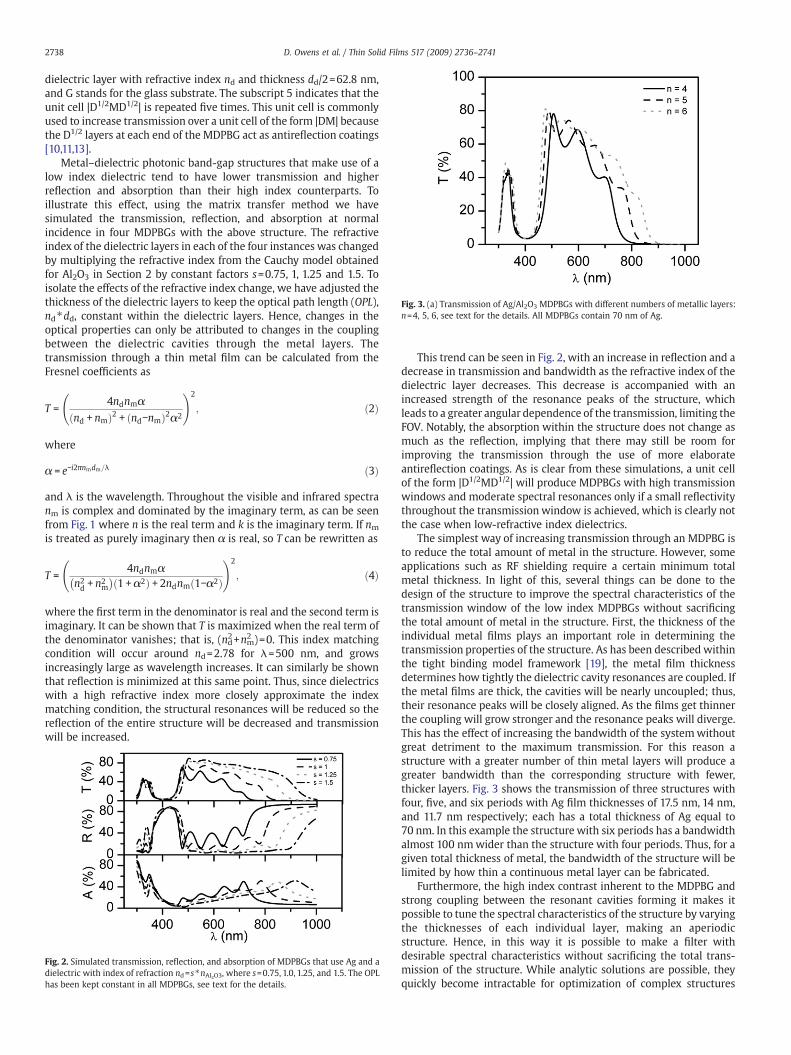
Fig. 3. (a) Transmission of Ag/Al2O3 MDPBGs with different numbers of metallic layers:n=4, 5, 6, see text for the details. All MDPBGs contain 70 nm of Ag.
2738 D. Owens et al. / Thin Solid Films 517 (2009) 2736–2741
dielectric layer with refractive index nd and thickness dd/2=62.8 nm,and G stands for the glass substrate. The subscript 5 indicates that theunit cell |D1/2MD1/2| is repeated five times. This unit cell is commonlyused to increase transmission over a unit cell of the form |DM| becausethe D1/2 layers at each end of the MDPBG act as antireflection coatings[10,11,13].
Metal–dielectric photonic band-gap structures that make use of alow index dielectric tend to have lower transmission and higherreflection and absorption than their high index counterparts. Toillustrate this effect, using the matrix transfer method we havesimulated the transmission, reflection, and absorption at normalincidence in four MDPBGs with the above structure. The refractiveindex of the dielectric layers in each of the four instances was changedby multiplying the refractive index from the Cauchy model obtainedfor Al2O3 in Section 2 by constant factors s=0.75, 1, 1.25 and 1.5. Toisolate the effects of the refractive index change, we have adjusted thethickness of the dielectric layers to keep the optical path length (OPL),nd⁎dd, constant within the dielectric layers. Hence, changes in theoptical properties can only be attributed to changes in the couplingbetween the dielectric cavities through the metal layers. Thetransmission through a thin metal film can be calculated from theFresnel coefficients as
T =4ndnmα
nd + nmð Þ2 + nd−nmð Þ2α2
!2
; ð2Þ
where
α = e−i2πnmdm=λ ð3Þ
and λ is the wavelength. Throughout the visible and infrared spectranm is complex and dominated by the imaginary term, as can be seenfrom Fig. 1 where n is the real term and k is the imaginary term. If nmis treated as purely imaginary then α is real, so T can be rewritten as
T =4ndnmα
n2d + n
2m
� �1 + α2ð Þ + 2ndnm 1−α2ð Þ
!2
; ð4Þ
where the first term in the denominator is real and the second term isimaginary. It can be shown that T is maximized when the real term ofthe denominator vanishes; that is, (nd2+nm2 )=0. This index matchingcondition will occur around nd=2.78 for λ=500 nm, and growsincreasingly large as wavelength increases. It can similarly be shownthat reflection is minimized at this same point. Thus, since dielectricswith a high refractive index more closely approximate the indexmatching condition, the structural resonances will be reduced so thereflection of the entire structure will be decreased and transmissionwill be increased.
Fig. 2. Simulated transmission, reflection, and absorption of MDPBGs that use Ag and adielectric with index of refraction nd=s⁎nAl2O3, where s=0.75, 1.0, 1.25, and 1.5. The OPLhas been kept constant in all MDPBGs, see text for the details.
This trend can be seen in Fig. 2, with an increase in reflection and adecrease in transmission and bandwidth as the refractive index of thedielectric layer decreases. This decrease is accompanied with anincreased strength of the resonance peaks of the structure, whichleads to a greater angular dependence of the transmission, limiting theFOV. Notably, the absorption within the structure does not change asmuch as the reflection, implying that there may still be room forimproving the transmission through the use of more elaborateantireflection coatings. As is clear from these simulations, a unit cellof the form |D1/2MD1/2| will produce MDPBGs with high transmissionwindows and moderate spectral resonances only if a small reflectivitythroughout the transmission window is achieved, which is clearly notthe case when low-refractive index dielectrics.
The simplest way of increasing transmission through an MDPBG isto reduce the total amount of metal in the structure. However, someapplications such as RF shielding require a certain minimum totalmetal thickness. In light of this, several things can be done to thedesign of the structure to improve the spectral characteristics of thetransmission window of the low index MDPBGs without sacrificingthe total amount of metal in the structure. First, the thickness of theindividual metal films plays an important role in determining thetransmission properties of the structure. As has been described withinthe tight binding model framework [19], the metal film thicknessdetermines how tightly the dielectric cavity resonances are coupled. Ifthe metal films are thick, the cavities will be nearly uncoupled; thus,their resonance peaks will be closely aligned. As the films get thinnerthe coupling will grow stronger and the resonance peaks will diverge.This has the effect of increasing the bandwidth of the systemwithoutgreat detriment to the maximum transmission. For this reason astructure with a greater number of thin metal layers will produce agreater bandwidth than the corresponding structure with fewer,thicker layers. Fig. 3 shows the transmission of three structures withfour, five, and six periods with Ag film thicknesses of 17.5 nm, 14 nm,and 11.7 nm respectively; each has a total thickness of Ag equal to70 nm. In this example the structure with six periods has a bandwidthalmost 100 nmwider than the structure with four periods. Thus, for agiven total thickness of metal, the bandwidth of the structure will belimited by how thin a continuous metal layer can be fabricated.
Furthermore, the high index contrast inherent to the MDPBG andstrong coupling between the resonant cavities forming it makes itpossible to tune the spectral characteristics of the structure by varyingthe thicknesses of each individual layer, making an aperiodicstructure. Hence, in this way it is possible to make a filter withdesirable spectral characteristics without sacrificing the total trans-mission of the structure. While analytic solutions are possible, theyquickly become intractable for optimization of complex structures
2739D. Owens et al. / Thin Solid Films 517 (2009) 2736–2741
across a wide wavelength band so the process is better handled by anumerical algorithm.
In order to demonstrate this approach we design a structure withflat passband transmission in the wavelength range of 475–625 nmusing an iterative optimization process. The optimization process firstadjusts the thickness of each layer in turnwith the goal of maximizingthe transmission within the desired band [λmin, λmax], which isquantified by the metric
M = ∑λmax
λmin
T : ð5Þ
The process continues adjusting the thicknesses of each layer untilthe metric is maximized. The resulting structure is then used as thestarting point for the second stage of optimization, which repeats theprocess of the first stage with the goal of minimizing the variancewithin the band,
M =1
n−1∑
λmax
λmin
ðT−T Þ2: ð6Þ
The resulting structure (AP) and its transmission spectrum areshown in Fig. 4, along with the equivalent periodic structure (P1) ofthe form described in Eq. (1) and a periodic structure with anasymmetric unit cell (P2):
AirjDMj5G: ð7Þ
In this case the average transmission of structure AP, 65.3%, isslightly less than the 69.3% average for the structure P1; however, the
Fig. 4. (a) Transmission of aperiodic MDPBG (AP) with structure (b), along with twoperiodic structures (P1 and P2). (Inset) Change in transmission at 30° angle of incidencefor periodic (P1 and P2) and aperiodic (AP) MDPBGs.
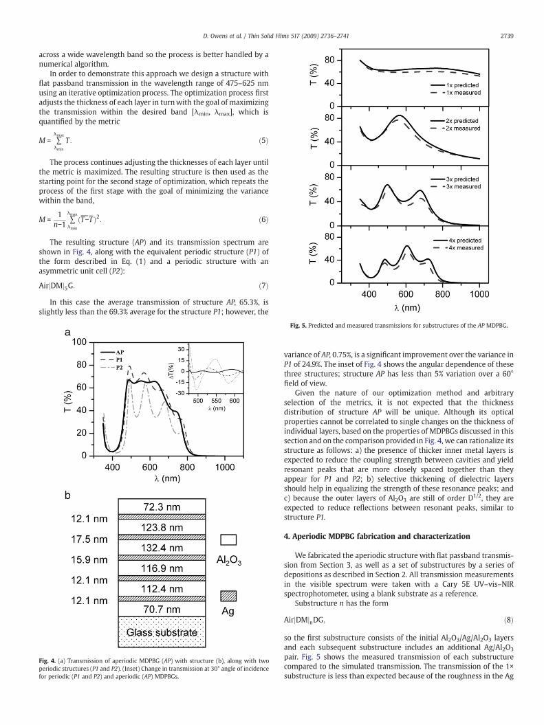
Fig. 5. Predicted and measured transmissions for substructures of the AP MDPBG.
variance of AP, 0.75%, is a significant improvement over the variance inP1 of 24.9%. The inset of Fig. 4 shows the angular dependence of thesethree structures; structure AP has less than 5% variation over a 60°field of view.
Given the nature of our optimization method and arbitraryselection of the metrics, it is not expected that the thicknessdistribution of structure AP will be unique. Although its opticalproperties cannot be correlated to single changes on the thickness ofindividual layers, based on the properties of MDPBGs discussed in thissection and on the comparisonprovided in Fig. 4, we can rationalize itsstructure as follows: a) the presence of thicker inner metal layers isexpected to reduce the coupling strength between cavities and yieldresonant peaks that are more closely spaced together than theyappear for P1 and P2; b) selective thickening of dielectric layersshould help in equalizing the strength of these resonance peaks; andc) because the outer layers of Al2O3 are still of order D1/2, they areexpected to reduce reflections between resonant peaks, similar tostructure P1.
4. Aperiodic MDPBG fabrication and characterization
We fabricated the aperiodic structure with flat passband transmis-sion from Section 3, as well as a set of substructures by a series ofdepositions as described in Section 2. All transmission measurementsin the visible spectrum were taken with a Cary 5E UV–vis–NIRspectrophotometer, using a blank substrate as a reference.
Substructure n has the form
AirjDMjnDG; ð8Þ
so the first substructure consists of the initial Al2O3/Ag/Al2O3 layersand each subsequent substructure includes an additional Ag/Al2O3
pair. Fig. 5 shows the measured transmission of each substructurecompared to the simulated transmission. The transmission of the 1×substructure is less than expected because of the roughness in the Ag

2740 D. Owens et al. / Thin Solid Films 517 (2009) 2736–2741
film, as seen in Fig. 1(b). This shortfall carries through the othersubstructures, though the general trend clearly follows thesimulations.
The transmission of the full fabricated AP structure is shown inFig. 6. This structure shows transmission of 53%±3% transmissionwith a 150 nm bandwidth between 475 nm and 625 nm. Thetransmission measurement, extended out to 5 μm through the use ofa Shimadzu IRPrestige Fourier Transform Infrared (FTIR) spectro-photometer, shows that the structure displays excellent rejectionof IR wavelengths beyond 800 nm. The measured transmissiondrops below 10−4 between 1 μm and 5 μm, giving excellent out ofband rejection through the infrared, where the MDPBG behaves likebulk Ag.
Fig. 6b shows the measured transmission spectrum of structure APat varying angles of incidence. As the angle of incidence is increasedthe passband shifts toward shorter wavelengths due to the negativepermittivity of the metal [20]. It can be seen that the measuredmagnitude of the angular dependence matches well with thepredicted values. Transmission in structure AP changes by less than5% over almost the entire range of the filter, giving a field-of-view thatis more than 60° wide.
Finally, Fig. 7 shows the environmental stability of the fabricatedstructure. Fig. 7(a) shows the transmission of an AP structureimmediately after fabrication compared to the transmission afterhaving been exposed to air for ten months. The transmission changesless than 4%, demonstrating that the Al2O3 acts as an effective barrierto the diffusion of oxygen into the metal. Fig. 7(b) shows thetransmission of the structure at temperatures ranging from room
Fig. 6. (a) Predicted and measured transmissions of AP MDPBG. (b) Transmission of APMDPBG measured at 0, 10, 20, and 30° angles of incidence. (Inset) Predicted andmeasured changes in transmission at 10, 20, and 30° angles of incidence for APMDPBG.
Fig. 7. (a) Transmission of AP MDPBG measured over ten months of exposure to air.(b) Transmission of AP MDPBG measured over temperatures up to 150 °C.
temperature up to 150 °C. In this case the transmission changes by lessthan 2%.
5. Conclusion
We have described and discussed some of the effects that usinglow-refractive index dielectric materials in MDPBG structures have ontheir optical properties. We demonstrated that the inherent highindex contrast in these structures makes is possible to tailor thespectral characteristics of the passbandwindow bymoving away fromstructures with thickness distributions that are strictly periodic. Toillustrate this approach we designed and fabricated, by electron beamdeposition, an aperiodic MDPBG using Ag and Al2O3, and compared itstransmission and angular dependence to the predicted values,validating the design and demonstrating that such structures can befabricated. The optical properties of the fabricated devices show littlesigns of degradation over a ten month period of time and arethermally stable at temperatures up to 150 °C. The strong increase inthe reflection losses, as opposed to absorption losses, when low-refractive index dielectrics are used, suggests that there may be designroutes for further optimization of the overall transmission of MDPBGs.
Acknowledgements
We would like to thank Prof. Vladimir Tsukruk and his group forletting us use their Spectroscopic Ellipsometer, Prof. Seth Marder andhis group for the use of their Cary, and Prof. Ken Sandhage and hisgroup for the use of their FTIR system. This work was partially fundedby NSF through STC-DMR-0120967 and by ARO through contract/grant 50372-CH-MUR.

2741D. Owens et al. / Thin Solid Films 517 (2009) 2736–2741
References
[1] M.M. Sigalas, C.T. Chan, K.M. Ho, C.M. Soukoulis, Phys. Rev. B 52 (1995) 11744.[2] S.H. Fan, P.R. Villeneuve, J.D. Joannopoulos, Phys. Rev. B 54 (1996) 11245.[3] J.G. Fleming, S.Y. Lin, I. El-Kady, R. Biswas, K.M. Ho, Nature 417 (2002) 52.[4] M.J. Bloemer, M. Scalora, App. Phys Lett 72 (1998) 1676.[5] B. Wood, J.B. Pendry, D.P. Tsai, Phys. Rev. B 74 (2006) 8.[6] R.S. Bennink, Y.K. Yoon, R.W. Boyd, J.E. Sipe, Opt. Lett. 24 (1999) 1416.[7] M. Scalora, M.J. Bloemer, A.S. Pethel, J.P. Dowling, C.M. Bowden, A.S. Manka, J. Appl.
Phys. 83 (1998) 2377.[8] R. Lopez, R. Ruiz, R.F. Haglund, L.C. Feldman, Appl. Phys. A-Mater. Sci. Process. 74
(2002) 307.[9] M.S. Sarto, F. Sarto, M.C. Larciprete, M. Scalora, M. D'Amore, C. Sibilia, M. Bertolotti,
IEEE Trans. Electromagn. Compat. 45 (2003) 586.[10] J.H. Lee, S.H. Lee, C.K. Kwangbo, K.S. Lee, J.Korean Phys. Soc. 44 (2004) 750.
[11] Z. Jaksic, M. Maksimovic, M. Sarajlic, J. Opt. A-Pure Appl. Opt. 7 (2005) 51.[12] Z.G. Wang, Q.L. Chen, X. Cai, Appl. Surf. Sci. 239 (2005) 262.[13] M.S. Sarto, R.L. Voti, F. Sarto, M.C. Larciprete, IEEE Trans. Electromagn. Compat. 47
(2005) 602.[14] Z.G. Wang, X. Cai, Q.L. Chen, L.H. Li, Vacuum 80 (2006) 438.[15] L.T. Zhang, W.F. Xie, J. Wang, H.Z. Zhang, Y.S. Zhang, J. Phys. D-Appl. Phys. 39 (2006)
2373.[16] I. Avrutsky, I. Salakhutdinov, J. Elser, V. Podolskiy, Phys. Rev. B 75 (2007).[17] T.S. Eriksson, A. Hjortsberg, G.A. Niklasson, C.G. Granqvist, Appl. Opt. 20 (1981)
2742.[18] M. Bayindir, B. Temelkuran, E. Ozbay, Phys. Rev. Lett. 84 (2000) 2140.[19] C.S. Kee, K. Kim, H. Lim, J. Opt. A-Pure Appl. Opt. 6 (2004) 22.[20] J.L. Zhang, H.T. Jiang, W.D. Shen, X. Liu, Y.Y. Li, P.F. Gu, J. Opt. Soc. Am. B-Opt. Phys.
25 (2008) 1474.