Embed Size (px)
Citation preview

Reflex Photonics Inc. Copyright © 2016 Page 1 of 13
Optical IC Package Product Family Summary Updated: 2016-08-10
Reflex Photonics Inc. Copyright © 2016 Page 2 of 13
Optical IC Packaging Product Family Summary The Light on Board optical IC packaging technology offered by Reflex Photonics Inc. brings together user-defined microchips (ASIC’s, FPGA’s, Processors, Switches, etc…) and modular optical engines to better enhance the i/o capabilities of standard packaging and board assemblies. Within the product family of optical IC packaging, several types of chip sets have been targeted; these include FPGA’s, Processors and Switch chips as examples of optically enabled technologies, but many other chips sets can also be included. However, the 3 flavors of targeted chips should offer a wide variety of applications to choose from, such as DSP, compute and Ethernet/InfiniBand switching/routing, especially in the case of the flexible FPGA technologies. The main benefits of the optical IC package technology include:
High performance 28G/56G signaling Smaller, integrated size Simplified motherboard construction (low-speed, power and control) Lower cost system assembly and materials Socketable and modular core functionality Field replaceable upgrades Ultra-dense faceplate port counts Lower electrical power consumption
Each of the optical IC packages outlined below might require additional hardware considerations such as socket-types for the motherboard, retention brackets, screw holes and screws, heatsinks, spring-release attachments, optical cable routing interconnects, as well as thermal-flow path considerations. Furthermore, some design considerations involving component placement, electrical trace line routing, and configuration circuitry may also be required during the initial design phase. These design consideration are normally application specific, but Reflex can help with all these aspects of the design.

Reflex Photonics Inc. Copyright © 2016 Page 3 of 13
Generic Package Description: The generic optical IC package is shown in figure 01. It shows at least 1 optical engine, 1 main chip (ASIC, FPGA, CPU, Switch, etc…), an interposer substrate, and a method of connecting to the main host board via a PGA (pin grid array), BGA (ball grid array) or an LGA (land grid array).
Figure 01 – Side View of Generic Optical IC Package
Given that the position of the optical engines is within 5 to 10 mm from the main packaged chip, the signal integrity, the emi noise, the impedance and the density of signals can all be optimized. With such short interconnects, the amount of pre-emphasis and equalization of the electrical signals can be at a minimum, and CDR functions and FEC can be eliminated, thereby drastically reducing the amount of electrical power required. Furthermore, because of the small distances involved, the ability to maintain very high data rates using a minimum of expensive material (such as GeTek or Rogers) is possible. Lastly, one of the most beneficial aspects of the design is that the optical ports are guaranteed to work for any design, since the package dynamics have all been worked out and customers need only to integrate the package into a system architecture without worrying about the signal integrity of the 28G signals. Optical IC Package Generic Specifications:
JEDEC compatible footprints 2.54, 1.27 and 1 millimeter pin/ball pitches Up to 21x21 PGA arrays (external to package) Up to 35x35 LGA arrays (external to package) Height of packages < 7.0-mm (excluding heatsinking)
Reflex Photonics Inc. Copyright © 2016 Page 4 of 13
From 4 to 192 bidirectional optical ports Custom packages available with variable ratios of input to output ports Optical transmitters support SR signaling with 850-nm VCSEL technology MT optical interfaces for 250-um pitch OM3 Multimode (50/125) optical fiber A multilayer interposer Impedance controlled for high-speed transmission lines Multiple Power Plane definitions Multiple Ground Plane definitions On-package filtering and de-coupling assemblies On-package power regulation Fully compatible with standard IC assembly and PCB assembly processes
Optical Engine Description: There are several flavors of optical engines that can be used with the optical IC package. They can be selected for the number of channels, the type of channel (input or output), the density of channels, their data rate per channel, and the ratio of input to output. All optical engines have similar electrical interfaces – these are BGA solder balls for SMT mounting. The signaling follow the standard CML/LVDS differential signaling using peak-to-peak voltages of 2.9 to 3.1V. They are normally AC-coupled to the main ASIC chip and have a lower data-rate of 1-Mbps. Each device can be directly addressed via a 2-wire serial interface or can be designed to be addressed through the main ASIC chip, exclusively. Their data-rates, depending on the version, can be from 10-Gbps to 28-Gbps per channel and some tuning of their electrical signaling can be done, but is generally adjusted and programmed during initial testing. The optical engine converts between electrical and optical signals using either a 1x12 array of 850-nm VCSELs or a 1x12 array of 850-nm PIN Photodetectors. A driver or receiver ASIC chip is used alongside the VCSEL or PD, respectively, to interface between the electrical CML signals and the optoelectronics. The optical interface uses a standard MT (multi-terminal) optical connector. The MT has 2 dowel-pin guide holes for alignment to the connector and either a linear set of 12 optical fiber tips, pitched at 250-um (a 1x12 MT interface), or 2 linear sets of 12 optical fibers, pitched at 500-um between rows and 250-um between fibers in a row (a 2x12 MT interface). The mating connector is an identical MT connector, but also requires a retention clip to secure the MT’s together.

Reflex Photonics Inc. Copyright © 2016 Page 5 of 13
An example of this type of optical engine is shown in the side figure. This shows a 10x10 BGA SMT part with a 1x12 MT optical interface (covered by the protective silicone boot). Its total size is roughly 13-mm wide by 24-mm long. It can be placed around the optical IC package and be either a 12-channel transmit module, a 12-channel receive module, or a 4-ch Transmit / 4-channel Receive “transceiver” module and it operates up to 14-Gbps per channel. Other optical engines include:
4- channel, bidirectional (4-Tx / 4-Rx) module at 12.5-Gbps per channel 12-channel Transmitter at 28-Gbps 12-channel Receiver at 28-Gbps 12-channel, bidirectional (12-Tx / 12-Rx) module at 28-Gbps per channel
Target Chip Sets: There are several targeted chip sets that have been designed into the optical IC package family of products. They are all nominally very large IC packages, roughly 45-mm on a side with many 10’s up to 100’s of high-speed differential electrical signals. The packages are normally cavity-up organic BGA’s that have anywhere from 900 BGA balls to 2500 BGA balls. The 3 main chip sets are for general FPGA, DSP/CPU, and Switch applications. These chip sets should be able to cover numerous applications spaces such as for wireless/LTE computing, Ethernet-MAC and InfiniBand switching systems, along with DSP processing nodes for video, broadcast and image-processing. The data rates will target 10G Ethernet speeds, PCI Express 3.0 or proprietary 12.5-Gbps optical links – as dictated as per the desired architecture. The most advanced FPGA and Switch chips will target data rates up to 28-Gbps per channel and would be targeted towards 100G and 400G Ethernet.

Reflex Photonics Inc. Copyright © 2016 Page 6 of 13
Product Family Overview: The following set of optical IC packages provide 6 different options for the customer to choose from. The base designs are based on industry available chip sets such as FPGA’s, Processors, and Switches, but the definition of the package along with certain aspects of the optical engine is modified under a separate and customized design program. Contact Reflex Sales ([email protected]) for more information. The family overview consist of:
- 36 BiDir Optical Channels at 12.5-Gbps with FPGA
- 24 BiDir Optical Channels at 12.5-Gbps with DualCore CPU
- 96 BiDir Optical Channels at 13.1-Gbps with FPGA
- 96 BiDir Optical Channels at 28.05-Gbps with FPGA
- 144 BiDir Optical Channels at 28.05-Gbps with Switch Chip
- 192 BiDir Optical Channels at 28.05-Gbps with Proprietary Chip
PULSAR
QUASAR
NOVA
SUPERNOVA
GALAXY
MAGNATAR

Reflex Photonics Inc. Copyright © 2016 Page 7 of 13
PULSAR The PULSAR optical IC package will use the Xilinx Kintex-7 FPGA. Specifically, the GTX version, model number: XC7K420T. It targets FPGA/DSP applications and has 416,960 logic cells with 400 generic single-ended i/o. This chip set has 32 differential high-speed i/o with data rates up to 12.5-Gbps. The package style is the Xilinx FFG1156 BGA package, 35-mm x 35-mm with a 1-mm ball pitch. There are 6 optical engines, 3 12-channel transmit module, and 3 12-channel receive modules. The optical engines are 10x10 1.27-mm BGA pitched SMT device, and have a 1x12 MT as the optical port. The package is shown as a PGA (pin-grid array) style package but can also be in both LGA and BGA (although BGA does require some custom modifications for multiple solder-reflow steps)

Reflex Photonics Inc. Copyright © 2016 Page 8 of 13
QUASAR The QUASAR optical IC package will use the Xilinx ZYNQ FPGA. Specifically, the Z-7045 model with a DualCore ARM processor. The chip set targets DSP and Compute applications and has 218,600 logic cells with 54 processing system i/o. This chip set has 16 differential high-speed i/o with data rates up to 12.5-Gbps. The package style is the Xilinx FFG900 BGA package, 31-mm x 31-mm with a 1-mm ball pitch. There are 4 optical engines, 2 12-channel transmit module, and 2 12-channel receive modules. The optical engines are 10x10 1.27-mm BGA pitched SMT device, and have a 1x12 MT as the optical port. The package is shown as a PGA (pin-grid array) style package but can also be in both LGA and BGA (although BGA does require some custom modifications for multiple solder-reflow steps)

Reflex Photonics Inc. Copyright © 2016 Page 9 of 13
GALAXY The GALAXY optical IC package targets the Xilinx Virtex-7 FPGA. Specifically, the GTH version, model number: XC7VX690T. This chip set targets multipurpose FPGA for compute, switching and networked array applications and has 693,120 logic cells with 1,000 generic i/o. This chip also has 80 GTX differential high-speed i/o with data rates up to 13.1-Gbps. The package style is the Xilinx FFG1930 BGA package, 45-mm x 45-mm with a 1-mm ball pitch. There are 16 optical engines, 8 12-channel transmit module, and 8 12-channel receive modules. The optical engines are 10x10 1.27-mm BGA pitched SMT device, and have a 1x12 MT as the optical port. The package is shown as a PGA (pin-grid array) style package but can also be in both LGA and BGA (although BGA does require some custom modifications for multiple solder-reflow steps)

Reflex Photonics Inc. Copyright © 2016 Page 10 of 13
NOVA The NOVA optical IC package targets the Xilinx Virtex-7 FPGA. Specifically, model number: XC7VH870T. This chip set is one of the largest and most powerful FPGAs in the market today. It is a multipurpose FPGA for intensive computing and switching applications and has 876,160 logic cells with 300 generic i/o. This chip also has 72 GTH serial transceivers at 13.1-Gbps and 16 GTZ serial transceivers at 28.05-Gbps. The package style is the Xilinx FFG1930 BGA package, 45-mm x 45-mm with a 1-mm ball pitch. There are 16 optical engines, 8 12-channel transmit module, and 8 12-channel receive modules. The optical engines are 12x12 1-mm BGA pitched SMT device, and have a 1x12 MT as the optical port. The package is shown as a PGA (pin-grid array) style package but can also be in both LGA and BGA (although BGA does require some custom modifications for multiple solder-reflow steps)

Reflex Photonics Inc. Copyright © 2016 Page 11 of 13
MAGNATAR The MAGNATAR optical IC package targets the newly introduced Broadcom Tomahawk Switch. This switch has 128 25-Gbps serial transceivers and is the most powerful aggregation switch in the market today. It supports the Ethernet 25/50/100GbE line rates and provides a total switching capacity of 3.2 Tbps. The MAGNATAR package therefore requires 12 optical engines, each one a 12-channel bidirectional module with 12 optical transmit and 12 optical receive ports in a single optical engine. The engine supports a 12x20 1-mm pitch BGA as an SMT device, and has a 2x12 MT as the optical port. The package is shown as a PGA (pin-grid array) style package but can also be in both LGA and BGA (although BGA does require some custom modifications for multiple solder-reflow steps)
Reflex Photonics Inc. Copyright © 2016 Page 12 of 13
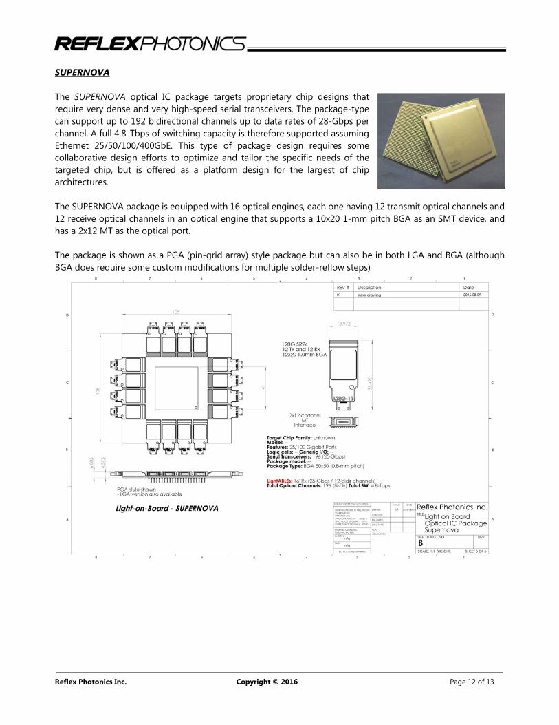
SUPERNOVA The SUPERNOVA optical IC package targets proprietary chip designs that require very dense and very high-speed serial transceivers. The package-type can support up to 192 bidirectional channels up to data rates of 28-Gbps per channel. A full 4.8-Tbps of switching capacity is therefore supported assuming Ethernet 25/50/100/400GbE. This type of package design requires some collaborative design efforts to optimize and tailor the specific needs of the targeted chip, but is offered as a platform design for the largest of chip architectures. The SUPERNOVA package is equipped with 16 optical engines, each one having 12 transmit optical channels and 12 receive optical channels in an optical engine that supports a 10x20 1-mm pitch BGA as an SMT device, and has a 2x12 MT as the optical port. The package is shown as a PGA (pin-grid array) style package but can also be in both LGA and BGA (although BGA does require some custom modifications for multiple solder-reflow steps)

Reflex Photonics Inc. Copyright © 2016 Page 13 of 13
Additional Hardware and Materials: For each of these package designs, and depending on the particular requirements of the system architecture, some additional packaging components will be required. Board mounted sub-components such as heatsinks, sockets, retention brackets and clips, optical fiber cables and connectors, screws and fans may be required. Most of these items will be commercial-off-the-shelf (COTS) parts, but some may require design and/or alteration as specified by the customer application. Furthermore, certain design constraints particular to the customer’s application, such as types of power-supply regulation, filtering, and passive component placement along with possible trace-line routing requirements, as well as material and board selection considerations may be required. Reflex Photonics can provide support and design services for each of these design considerations. Note that depending on the mix of high-speed serial transceivers, the specific applications required of the chip-set, and if certain i/o must be routed electrically within the host-board itself, different socket technology may have to be considered.