Embed Size (px)
Citation preview
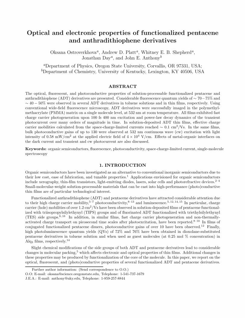
Optical and electronic properties of functionalized pentacene
and anthradithiophene derivatives
Oksana Ostroverkhovaa, Andrew D. Platta, Whitney E. B. Shepherda,
Jonathan Daya, and John E. Anthonyb
aDepartment of Physics, Oregon State University, Corvallis, OR 97331, USA;bDepartment of Chemistry, University of Kentucky, Lexington, KY 40506, USA
ABSTRACT
The optical, fluorescent, and photoconductive properties of solution-processable functionalized pentacene andanthradithiophene (ADT) derivatives are presented. Considerable fluorescence quantum yields of ∼ 70−75% and∼ 40− 50% were observed in several ADT derivatives in toluene solutions and in thin films, respectively. Usingconventional wide-field fluorescence microscopy, ADT derivatives were successfully imaged in the polymethyl-methacrylate (PMMA) matrix on a single molecule level, at 532 nm at room temperature. All films exhibited fastcharge carrier photogeneration upon 100 fs 400 nm excitation and power-law decay dynamics of the transientphotocurrent over many orders of magnitude in time. In solution-deposited ADT thin films, effective chargecarrier mobilities calculated from the space-charge-limited currents reached ∼ 0.1 cm2/Vs. In the same films,bulk photoconductive gains of up to 130 were observed at 532 nm continuous wave (cw) excitation with lightintensity of 0.58 mW/cm2 at the applied electric field of 4 × 10⁴ V/cm. Effects of metal-organic interfaces onthe dark current and transient and cw photocurrent are also discussed.
Keywords: organic semiconductors, fluorescence, photoconductivity, space-charge-limited current, single-moleculespectroscopy
1. INTRODUCTION
Organic semiconductors have been investigated as an alternative to conventional inorganic semiconductors due totheir low cost, ease of fabrication, and tunable properties.1 Applications envisioned for organic semiconductorsinclude xerography, thin-film transistors, light-emitting diodes, lasers, solar cells and photorefractive devices.2–4
Small-molecular-weight solution-processable materials that can be cast into high-performance (photo)conductivethin films are of particular technological interest.
Functionalized anthradithiophene (ADT) and pentacene derivatives have attracted considerable attention dueto their high charge carrier mobility,5–7 photoconductivity,8–13 and luminescence.5, 12, 14, 15 In particular, chargecarrier (hole) mobilities of over 1.2 cm2/Vs have been observed in solution-deposited films of pentacene functional-ized with triisopropylsilylethynyl (TIPS) groups and of fluorinated ADT functionalized with triethylsilylethynyl(TES) side groups.6, 16 In addition, in similar films, fast charge carrier photogeneration and non-thermally-activated charge transport on picosecond time scales after photoexcitation, have been reported.8–10 In films ofconjugated functionalized pentacene dimers, photoconductive gains of over 10 have been observed.12 Finally,high photoluminescence quantum yields (QYs) of 72% and 76% have been obtained in dioxolane-substitutedpentacene derivatives in toluene solution and when used as guest molecules (at 0.25 mol % concentration) inAlq3 films, respectively.14
Slight chemical modifications of the side groups of both ADT and pentacene derivatives lead to considerablechanges in molecular packing,5 which affects electronic and optical properties of thin films. Additional changes inthese properties may be produced by functionalization of the core of the molecule. In this paper, we report on theoptical, fluorescent, and (photo)conductive properties of several functionalized ADT and pentacene derivatives.
Further author information: (Send correspondence to O.O.)O.O: E-mail: [email protected], Telephone: 1-541-737-1679J.E.A.: E-mail: [email protected], Telephone: 1-859-257-8844
Si
Si(a)
S
S
R
R
R’ R’
(b)
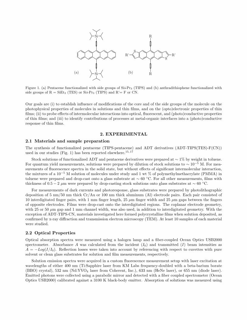
Figure 1. (a) Pentacene functionalized with side groups of Sii-Pr3 (TIPS) and (b) anthradithiophene functionalized withside groups of R = SiEt3 (TES) or Sii-Pr3 (TIPS) and R’= F or CN.
Our goals are (i) to establish influence of modifications of the core and of the side groups of the molecule on thephotophysical properties of molecules in solutions and thin films, and on the (opto)electronic properties of thinfilms; (ii) to probe effects of intermolecular interactions into optical, fluorescent, and (photo)conductive propertiesof thin films; and (iii) to identify contributions of processes at metal-organic interfaces into a (photo)conductiveresponse of thin films.
2. EXPERIMENTAL
2.1 Materials and sample preparation
The synthesis of functionalized pentacene (TIPS-pentacene) and ADT derivatives (ADT-TIPS(TES)-F(CN))used in our studies (Fig. 1) has been reported elsewhere.15, 17
Stock solutions of functionalized ADT and pentacene derivatives were prepared at ∼ 1% by weight in toluene.For quantum yield measurements, solutions were prepared by dilution of stock solutions to ∼ 10−5 M. For mea-surements of fluorescence spectra in the solid state, but without effects of significant intermolecular interaction,the mixtures of a 10−5 M solution of molecules under study and 1 wt % of polymethylmethacrylate (PMMA) intoluene were prepared and drop-cast onto a glass substrate at ∼ 60 C. For all other measurements, films withthickness of 0.5 − 2 µm were prepared by drop-casting stock solutions onto glass substrates at ∼ 60 C.
For measurements of dark currents and photoresponse, glass substrates were prepared by photolithographicdeposition of 5 nm/50 nm thick Cr/Au or 100 nm thick aluminum (Al) electrode pairs. Each pair consisted of10 interdigitated finger pairs, with 1 mm finger length, 25 µm finger width and 25 µm gaps between the fingersof opposite electrodes. Films were drop-cast onto the interdigitated regions. The coplanar electrode geometry,with 25 or 50 µm gap and 1 mm channel width, was also used, in addition to interdigitated geometry. With theexception of ADT-TIPS-CN, materials investigated here formed polycrystalline films when solution deposited, asconfirmed by x-ray diffraction and transmission electron microscopy (TEM). At least 10 samples of each materialwere studied.
2.2 Optical Properties
Optical absorption spectra were measured using a halogen lamp and a fiber-coupled Ocean Optics USB2000spectrometer. Absorbance A was calculated from the incident (I0) and transmitted (I) beam intensities asA = −Log(I/I0). Reflection losses were taken into account by referencing with respect to cuvettes with puresolvent or clean glass substrates for solution and film measurements, respectively.
Solution emission spectra were acquired in a custom fluorescence measurement setup with laser excitation atwavelengths of either 400 nm (Ti:Sapphire laser from KM Labs frequency-doubled with a beta-barium borate(BBO) crystal), 532 nm (Nd:YVO4 laser from Coherent, Inc.), 633 nm (HeNe laser), or 655 nm (diode laser).Emitted photons were collected using a parabolic mirror and detected with a fiber coupled spectrometer (OceanOptics USB2000) calibrated against a 3100 K black-body emitter. Absorption of solutions was measured using
a standard 1 cm path length quartz cuvette with a halogen light source fiber-optically delivered to the sampleholder and spectrometer. Fluorescence quantum yields (QYs) in solution were referenced against standardswith known quantum yields and corrected for differences in optical density and solvent refractive index.18 TheADT derivatives were measured against rhodamine 6G in ethanol (Φf = 0.95) and DCDHF-N-6 in toluene(Φf = 0.85).19 The QY of TIPS pentacene solution was measured against rhodamine 6G in ethanol and AlexaFluor 647 in a phosphate buffer solution (pH 7.2, Φf = 0.33).20 The QYs in films were estimated using DCDHF-N-6 in PMMA (Φf = 0.98)19 as a reference and assuming a value of 1.7 for the index of refraction. The detectionlimit of the setup was estimated to be at QY≈0.5%.
Fluorescence lifetime measurements were performed using a frequency-doubled mode-locked Ti:Sapphire laserwith a repetition rate of 93 MHz picked at 9.3 MHz using a home-built pulse picker (based on a TeO2 acousto-optic modulator from NEOS) and pulses 80 fs in length as the excitation source. A single-photon avalanchephotodiode (SPAD – Molecular Photonic Devices) was used in conjunction with a time-correlated single-photoncounter (TCSPC) data analysis board (PicoQuant TimeHarp 200) for detection. The instrument responsefunction (IRF) (∼ 200 ps) was recorded using scattered light from an etched microscope slide.
2.3 Single-molecule-level fluorescence imaging
Samples for fluorescence imaging at the single-molecule level were prepared from stock solutions of 1% by weightPMMA (75,000 m.w.) in toluene. ADT-TES-F was doped into the solution at the level of 10−10 per PMMApolymer. This solution was then spun coat onto clean glass coverslips at 2000 rpm for 55 s.
The samples were imaged with an Olympus IX71 inverted microscope with a 100X UPlanApo objective underwide-field 532 nm cw illumination. The fluorescence was detected by an Andor iXon DU-897 EMCCD camera.
2.4 Dark current and transient and cw photocurrent measurements
For transient photoconductivity measurements, an amplified Ti:Sapphire laser (800 nm, 100 fs, 1 kHz) was usedin conjunction with a frequency-doubling BBO crystal to excite the samples. Voltage was supplied by a Keithley237 source-measure unit, and light pulse-induced transient photocurrent was measured with a 50 Ω load by a50 GHz CSA8200 digital sampling oscilloscope.10, 11, 15, 21 Average electric field E was calculated as E = V/L,where V is the applied voltage, and L is the gap between the electrodes. For dark current and cw photocurrentmeasurements, the Keithley 237 source-measure unit was used to measure current through the sample in theabsence and in the presence of cw photoexcitation with a Nd:YVO4 laser at 532 nm. The cw photocurrent wascalculated as the difference between the two.
3. RESULTS AND DISCUSSION
3.1 Optical properties in solution
0
0.2
0.4
0.6
0.8
1
400 500 600
Abs
orba
nce
(arb
. u.)
Wavelength (nm)
(a)
500 600 700 800
0
0.2
0.4
0.6
0.8
1
Fluo
resc
ence
(ar
b. u
.)
Wavelength (nm)
(b) TIPS pentaceneADT-TIPS-CN
ADT-TIPS-FADT-TES-F
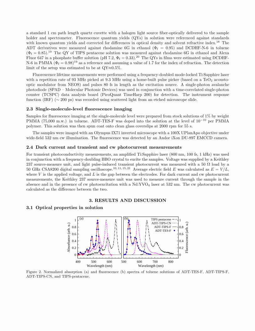
Figure 2. Normalized absorption (a) and fluorescence (b) spectra of toluene solutions of ADT-TES-F, ADT-TIPS-F,ADT-TIPS-CN, and TIPS-pentacene.
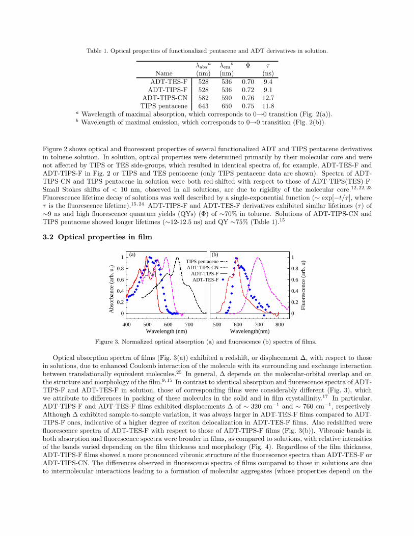
Table 1. Optical properties of functionalized pentacene and ADT derivatives in solution.
λabsa λem
b Φ τName (nm) (nm) (ns)
ADT-TES-F 528 536 0.70 9.4ADT-TIPS-F 528 536 0.72 9.1
ADT-TIPS-CN 582 590 0.76 12.7TIPS pentacene 643 650 0.75 11.8
a Wavelength of maximal absorption, which corresponds to 0→0 transition (Fig. 2(a)).b Wavelength of maximal emission, which corresponds to 0→0 transition (Fig. 2(b)).
Figure 2 shows optical and fluorescent properties of several functionalized ADT and TIPS pentacene derivativesin toluene solution. In solution, optical properties were determined primarily by their molecular core and werenot affected by TIPS or TES side-groups, which resulted in identical spectra of, for example, ADT-TES-F andADT-TIPS-F in Fig. 2 or TIPS and TES pentacene (only TIPS pentacene data are shown). Spectra of ADT-TIPS-CN and TIPS pentacene in solution were both red-shifted with respect to those of ADT-TIPS(TES)-F.Small Stokes shifts of < 10 nm, observed in all solutions, are due to rigidity of the molecular core.12, 22, 23
Fluorescence lifetime decay of solutions was well described by a single-exponential function (∼ exp[−t/τ ], whereτ is the fluorescence lifetime).15, 24 ADT-TIPS-F and ADT-TES-F derivatives exhibited similar lifetimes (τ) of∼9 ns and high fluorescence quantum yields (QYs) (Φ) of ∼70% in toluene. Solutions of ADT-TIPS-CN andTIPS pentacene showed longer lifetimes (∼12-12.5 ns) and QY ∼75% (Table 1).15
3.2 Optical properties in film
0
0.2
0.4
0.6
0.8
1
400 500 600 700
Abs
orba
nce
(arb
. u.)
Wavelength (nm)
(a)TIPS pentaceneADT-TIPS-CN
ADT-TIPS-FADT-TES-F
500 600 700 800
0
0.2
0.4
0.6
0.8
1
Fluo
resc
ence
(ar
b. u
)
Wavelength(nm)
(b)
Figure 3. Normalized optical absorption (a) and fluorescence (b) spectra of films.
Optical absorption spectra of films (Fig. 3(a)) exhibited a redshift, or displacement ∆, with respect to thosein solutions, due to enhanced Coulomb interaction of the molecule with its surrounding and exchange interactionbetween translationally equivalent molecules.25 In general, ∆ depends on the molecular-orbital overlap and onthe structure and morphology of the film.9, 15 In contrast to identical absorption and fluorescence spectra of ADT-TIPS-F and ADT-TES-F in solution, those of corresponding films were considerably different (Fig. 3), whichwe attribute to differences in packing of these molecules in the solid and in film crystallinity.17 In particular,ADT-TIPS-F and ADT-TES-F films exhibited displacements ∆ of ∼ 320 cm−1 and ∼ 760 cm−1, respectively.Although ∆ exhibited sample-to-sample variation, it was always larger in ADT-TES-F films compared to ADT-TIPS-F ones, indicative of a higher degree of exciton delocalization in ADT-TES-F films. Also redshifted werefluorescence spectra of ADT-TES-F with respect to those of ADT-TIPS-F films (Fig. 3(b)). Vibronic bands inboth absorption and fluorescence spectra were broader in films, as compared to solutions, with relative intensitiesof the bands varied depending on the film thickness and morphology (Fig. 4). Regardless of the film thickness,ADT-TIPS-F films showed a more pronounced vibronic structure of the fluorescence spectra than ADT-TES-F orADT-TIPS-CN. The differences observed in fluorescence spectra of films compared to those in solutions are dueto intermolecular interactions leading to a formation of molecular aggregates (whose properties depend on the
degree of molecular order, size, and intermolecular coupling).26–28 This is further supported by our observationsthat the fluorescence spectra of molecules under study embedded at low concentrations in the PMMA matrix(Fig. 4) yielded spectra identical to those of solutions in Fig. 1(b), as expected from non-interacting molecules.29
Although all materials studied could be prone to aggregate formation due to their π-stacking properties,5, 17
fluorescent properties of aggregates significantly depended on the material. For example, at room temperature,thin films of ADT-TIPS-F and ADT-TES-F were highly fluorescent, with QYs of at least 40 − 50% dependingon the film thickness and morphology. (These values represent a lower limit, since effects of self-absorption weresignificant in even the thinnest of our films). In contrast, fluorescence in TIPS pentacene films was considerablyweaker (QYs of < 0.5%). In all ADT films studied, QYs were strongly temperature-dependent, as described indetail in Refs. 15 and 24.
0
0.2
0.4
0.6
0.8
1
500 600 700 800
Fluo
resc
ence
(ar
b. u
.)
Wavelength (nm)
ADT-TIPS-F
PMMAabc
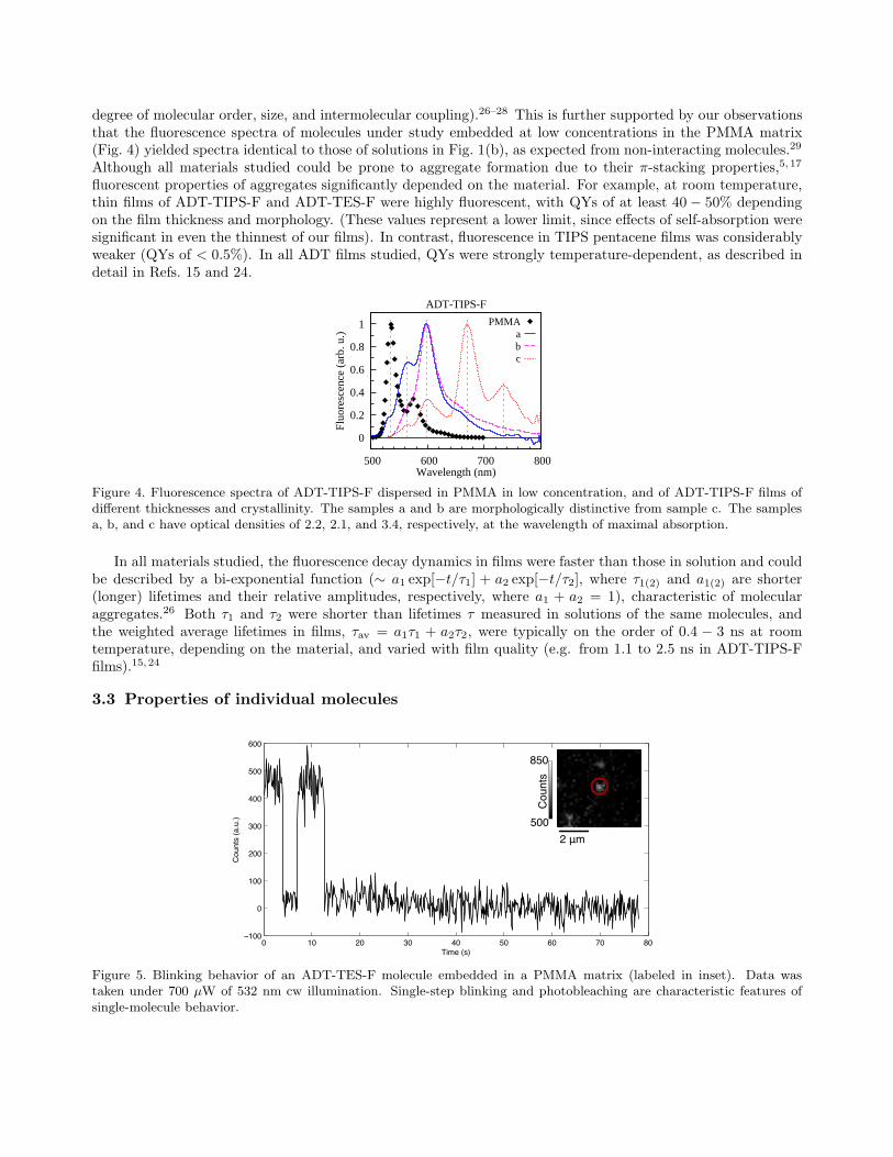
Figure 4. Fluorescence spectra of ADT-TIPS-F dispersed in PMMA in low concentration, and of ADT-TIPS-F films ofdifferent thicknesses and crystallinity. The samples a and b are morphologically distinctive from sample c. The samplesa, b, and c have optical densities of 2.2, 2.1, and 3.4, respectively, at the wavelength of maximal absorption.
In all materials studied, the fluorescence decay dynamics in films were faster than those in solution and couldbe described by a bi-exponential function (∼ a1 exp[−t/τ1] + a2 exp[−t/τ2], where τ1(2) and a1(2) are shorter(longer) lifetimes and their relative amplitudes, respectively, where a1 + a2 = 1), characteristic of molecularaggregates.26 Both τ1 and τ2 were shorter than lifetimes τ measured in solutions of the same molecules, andthe weighted average lifetimes in films, τav = a1τ1 + a2τ2, were typically on the order of 0.4 − 3 ns at roomtemperature, depending on the material, and varied with film quality (e.g. from 1.1 to 2.5 ns in ADT-TIPS-Ffilms).15, 24
3.3 Properties of individual molecules
! "! #! $! %! &! '! (! )!!"!!
!
"!!
#!!
$!!
%!!
&!!
'!!
*+,-./01
234560./78481
850
500
Counts
2 μm
Figure 5. Blinking behavior of an ADT-TES-F molecule embedded in a PMMA matrix (labeled in inset). Data wastaken under 700 µW of 532 nm cw illumination. Single-step blinking and photobleaching are characteristic features ofsingle-molecule behavior.
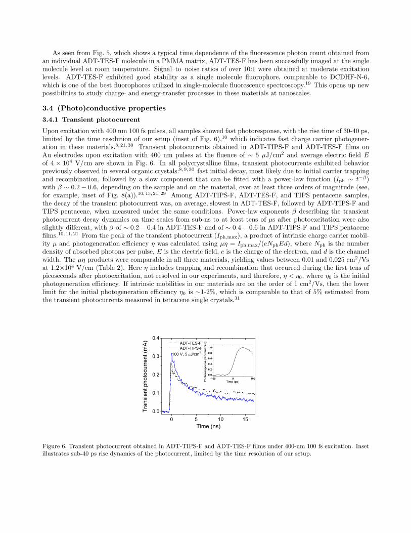
As seen from Fig. 5, which shows a typical time dependence of the fluorescence photon count obtained froman individual ADT-TES-F molecule in a PMMA matrix, ADT-TES-F has been successfully imaged at the singlemolecule level at room temperature. Signal–to–noise ratios of over 10:1 were obtained at moderate excitationlevels. ADT-TES-F exhibited good stability as a single molecule fluorophore, comparable to DCDHF-N-6,which is one of the best fluorophores utilized in single-molecule fluorescence spectroscopy.19 This opens up newpossibilities to study charge- and energy-transfer processes in these materials at nanoscales.
3.4 (Photo)conductive properties
3.4.1 Transient photocurrent
Upon excitation with 400 nm 100 fs pulses, all samples showed fast photoresponse, with the rise time of 30-40 ps,limited by the time resolution of our setup (inset of Fig. 6),10 which indicates fast charge carrier photogener-ation in these materials.8, 21, 30 Transient photocurrents obtained in ADT-TIPS-F and ADT-TES-F films onAu electrodes upon excitation with 400 nm pulses at the fluence of ∼ 5 µJ/cm2 and average electric field Eof 4 × 10⁴ V/cm are shown in Fig. 6. In all polycrystalline films, transient photocurrents exhibited behaviorpreviously observed in several organic crystals:8, 9, 30 fast initial decay, most likely due to initial carrier trappingand recombination, followed by a slow component that can be fitted with a power-law function (Iph ∼ t−β)with β ∼ 0.2 − 0.6, depending on the sample and on the material, over at least three orders of magnitude (see,for example, inset of Fig. 8(a)).10, 15, 21, 29 Among ADT-TIPS-F, ADT-TES-F, and TIPS pentacene samples,the decay of the transient photocurrent was, on average, slowest in ADT-TES-F, followed by ADT-TIPS-F andTIPS pentacene, when measured under the same conditions. Power-law exponents β describing the transientphotocurrent decay dynamics on time scales from sub-ns to at least tens of µs after photoexcitation were alsoslightly different, with β of ∼ 0.2 − 0.4 in ADT-TES-F and of ∼ 0.4 − 0.6 in ADT-TIPS-F and TIPS pentacenefilms.10, 11, 21 From the peak of the transient photocurrent (Iph,max), a product of intrinsic charge carrier mobil-ity µ and photogeneration efficiency η was calculated using µη = Iph,max/(eNphEd), where Nph is the numberdensity of absorbed photons per pulse, E is the electric field, e is the charge of the electron, and d is the channelwidth. The µη products were comparable in all three materials, yielding values between 0.01 and 0.025 cm2/Vsat 1.2×10⁴ V/cm (Table 2). Here η includes trapping and recombination that occurred during the first tens ofpicoseconds after photoexcitation, not resolved in our experiments, and therefore, η < η0, where η0 is the initialphotogeneration efficiency. If intrinsic mobilities in our materials are on the order of 1 cm2/Vs, then the lowerlimit for the initial photogeneration efficiency η0 is ∼1-2%, which is comparable to that of 5% estimated fromthe transient photocurrents measured in tetracene single crystals.31
-100 0 1000.0
0.2
0.4
0.6
0.8
1.0
Time (ps)Phot
ores
pons
e (N
orm
aliz
ed)
0 5 10 150.0
0.1
0.2
0.3
0.4
Tran
sien
t pho
tocu
rren
t (m
A)
Time (ns)
ADT-TES-F ADT-TIPS-F
100 V, 5 J/cm2
Figure 6. Transient photocurrent obtained in ADT-TIPS-F and ADT-TES-F films under 400-nm 100 fs excitation. Insetillustrates sub-40 ps rise dynamics of the photocurrent, limited by the time resolution of our setup.
3.4.2 Dark current
Space-charge-limited currents (SCLCs) were observed in the ADT-TIPS-F, ADT-TES-F and TIPS pentacenefilms on Au electrodes.11, 15 Effective charge carrier mobilities (µeff) were calculated from the slope of the fits ofthe dark current as a function of applied voltage squared. In the case of planar electrode geometry used here, thecurrent flows along a layer of unknown thickness, and there is no analytical solution for the relationship betweenSCLC (linear) density (j = Id/d, where Id is the dark current and d is the channel width) and voltage (V )in a film of finite thickness.11, 32 In the approximation of the infinitely thin film, valid when the film thicknessis much lower than the gap width (L) between the electrodes (which is the case here), j = 2µeffǫǫ0V
2/(πL2),where ǫ is a relative dielectric constant of the film and ǫ0 is the dielectric permittivity of vacuum. SCLC effectivemobilities (µeff), which represent a lower bound of charge carrier mobilities in these films, showed sample-to-sample variation, especially significant in the case of ADT-TIPS-F and TIPS pentacene (Table 2). On average,however, µeff in ADT-TES-F was at least a factor of ∼3 higher than that in ADT-TIPS-F, and a factor of ∼7higher than in TIPS pentacene films. A much lower current was observed in ADT-TIPS-CN films, which was aresult of both poor hole injection from Au contact due to a relatively high barrier of ∼0.45 eV Au forms withADT-TIPS-CN and the amorphous nature of the film. The effective mobility µeff = µθ, where θ is the ratiobetween free and trapped charge carriers (θ ≤1) is lower than the intrinsic mobility µ, since most likely the trap-free limit has not been achieved in our samples.33 Indeed, although µeff values of 0.033− 0.092 cm2/Vs obtainedin ADT-TES-F films were similar to those obtained in ADT-TES-F TFTs with channel lengths similar to ours(i.e. 25 µm),7 mobilities of over 1.5 cm2/Vs and 6 cm2/Vs have been achieved in short-channel ADT-TES-F filmsspin-coated on the Au electrodes treated with pentafluorobenzenethiol6, 17 and in ADT-TES-F single crystals,34
respectively. Therefore, θ is below ∼0.015 in our ADT-TES-F films. It is lower yet in TIPS pentacene films,since µeff values of 0.002− 0.007 cm2/Vs obtained in our SCLC measurements are much lower than 1.2 cm2/Vsobserved in TIPS pentacene TFTs,16 indicative of high trap density in our TIPS pentacene films.
10 100
0.1
1
10
100
1000
10000
100000
Applied voltage V (V)
ADT-TIPS-CN ADT-TIPS-F ADT-TES-F TIPS pentacene
Pho
tocu
rren
t (nA
)
532 nm0.58 mW/cm2
Figure 7. Cw photocurrent obtained in ADT-TES-F, ADT-TIPS-F, ADT-TIPS-CN, and TIPS pentacene films on inter-digitated Au electrodes as a function of applied voltage.
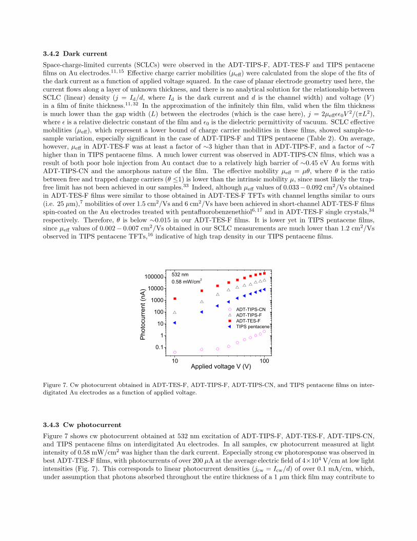
3.4.3 Cw photocurrent
Figure 7 shows cw photocurrent obtained at 532 nm excitation of ADT-TIPS-F, ADT-TES-F, ADT-TIPS-CN,and TIPS pentacene films on interdigitated Au electrodes. In all samples, cw photocurrent measured at lightintensity of 0.58 mW/cm2 was higher than the dark current. Especially strong cw photoresponse was observed inbest ADT-TES-F films, with photocurrents of over 200 µA at the average electric field of 4×10⁴ V/cm at low lightintensities (Fig. 7). This corresponds to linear photocurrent densities (jcw = Icw/d) of over 0.1 mA/cm, which,under assumption that photons absorbed throughout the entire thickness of a 1 µm thick film may contribute to
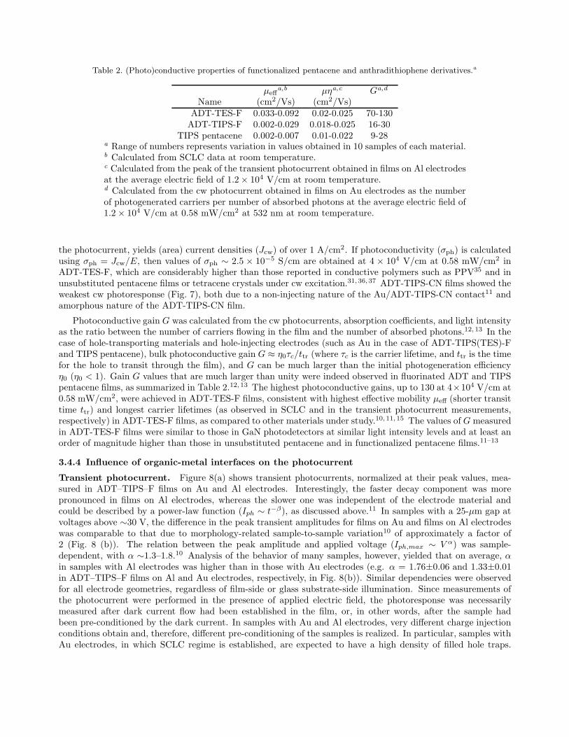
Table 2. (Photo)conductive properties of functionalized pentacene and anthradithiophene derivatives.a
µeffa,b µηa,c Ga,d
Name (cm2/Vs) (cm2/Vs)ADT-TES-F 0.033-0.092 0.02-0.025 70-130
ADT-TIPS-F 0.002-0.029 0.018-0.025 16-30TIPS pentacene 0.002-0.007 0.01-0.022 9-28
a Range of numbers represents variation in values obtained in 10 samples of each material.b Calculated from SCLC data at room temperature.c Calculated from the peak of the transient photocurrent obtained in films on Al electrodesat the average electric field of 1.2 × 10⁴ V/cm at room temperature.d Calculated from the cw photocurrent obtained in films on Au electrodes as the numberof photogenerated carriers per number of absorbed photons at the average electric field of1.2 × 104 V/cm at 0.58 mW/cm2 at 532 nm at room temperature.
the photocurrent, yields (area) current densities (Jcw) of over 1 A/cm2. If photoconductivity (σph) is calculatedusing σph = Jcw/E, then values of σph ∼ 2.5 × 10⁻⁵ S/cm are obtained at 4 × 10⁴ V/cm at 0.58 mW/cm2 inADT-TES-F, which are considerably higher than those reported in conductive polymers such as PPV35 and inunsubstituted pentacene films or tetracene crystals under cw excitation.31, 36, 37 ADT-TIPS-CN films showed theweakest cw photoresponse (Fig. 7), both due to a non-injecting nature of the Au/ADT-TIPS-CN contact11 andamorphous nature of the ADT-TIPS-CN film.
Photoconductive gain G was calculated from the cw photocurrents, absorption coefficients, and light intensityas the ratio between the number of carriers flowing in the film and the number of absorbed photons.12, 13 In thecase of hole-transporting materials and hole-injecting electrodes (such as Au in the case of ADT-TIPS(TES)-Fand TIPS pentacene), bulk photoconductive gain G ≈ η0τc/ttr (where τc is the carrier lifetime, and ttr is the timefor the hole to transit through the film), and G can be much larger than the initial photogeneration efficiencyη0 (η0 < 1). Gain G values that are much larger than unity were indeed observed in fluorinated ADT and TIPSpentacene films, as summarized in Table 2.12, 13 The highest photoconductive gains, up to 130 at 4×10⁴ V/cm at0.58 mW/cm2, were achieved in ADT-TES-F films, consistent with highest effective mobility µeff (shorter transittime ttr) and longest carrier lifetimes (as observed in SCLC and in the transient photocurrent measurements,respectively) in ADT-TES-F films, as compared to other materials under study.10, 11, 15 The values of G measuredin ADT-TES-F films were similar to those in GaN photodetectors at similar light intensity levels and at least anorder of magnitude higher than those in unsubstituted pentacene and in functionalized pentacene films.11–13
3.4.4 Influence of organic-metal interfaces on the photocurrent
Transient photocurrent. Figure 8(a) shows transient photocurrents, normalized at their peak values, mea-sured in ADT–TIPS–F films on Au and Al electrodes. Interestingly, the faster decay component was morepronounced in films on Al electrodes, whereas the slower one was independent of the electrode material andcould be described by a power-law function (Iph ∼ t−β), as discussed above.11 In samples with a 25-µm gap atvoltages above ∼30 V, the difference in the peak transient amplitudes for films on Au and films on Al electrodeswas comparable to that due to morphology-related sample-to-sample variation10 of approximately a factor of2 (Fig. 8 (b)). The relation between the peak amplitude and applied voltage (Iph,max ∼ V α) was sample-dependent, with α ∼1.3–1.8.10 Analysis of the behavior of many samples, however, yielded that on average, αin samples with Al electrodes was higher than in those with Au electrodes (e.g. α = 1.76±0.06 and 1.33±0.01in ADT–TIPS–F films on Al and Au electrodes, respectively, in Fig. 8(b)). Similar dependencies were observedfor all electrode geometries, regardless of film-side or glass substrate-side illumination. Since measurements ofthe photocurrent were performed in the presence of applied electric field, the photoresponse was necessarilymeasured after dark current flow had been established in the film, or, in other words, after the sample hadbeen pre-conditioned by the dark current. In samples with Au and Al electrodes, very different charge injectionconditions obtain and, therefore, different pre-conditioning of the samples is realized. In particular, samples withAu electrodes, in which SCLC regime is established, are expected to have a high density of filled hole traps.
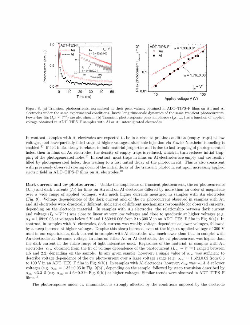
0 10 20 30 40 500.0
0.5
1.0
Pho
tocu
rren
t (ar
b.u.
)
Time (ns)
Au Al
ADT-TES-F
10 1000.01
0.1
1
Time (ns)
Iph~ t
Al = 0.45±0.01
Au = 0.450±0.003
10 1000.01
0.1
1
Pea
k ph
otoc
urre
nt I ph
,max
(mA
)
Applied voltage V (V)
Iph~ V
ADT-TIPS-F Au Al
= 1.33±0.01
= 1.76±0.06
Figure 8. (a) Transient photocurrents, normalized at their peak values, obtained in ADT–TIPS–F films on Au and Alelectrodes under the same experimental conditions. Inset: long time-scale dynamics of the same transient photocurrents.Power-law fits (Iph ∼ t−β) are also shown. (b) Transient photoresponse peak amplitude (Iph,max) as a function of appliedvoltage obtained in ADT–TIPS–F samples with Al or Au interdigitated electrodes.
In contrast, samples with Al electrodes are expected to be in a close-to-pristine condition (empty traps) at lowvoltages, and have partially filled traps at higher voltages, after hole injection via Fowler-Northeim tunneling isenabled.11 If fast initial decay is related to bulk material properties and is due to fast trapping of photogeneratedholes, then in films on Au electrodes, the density of empty traps is reduced, which in turn reduces initial trap-ping of the photogenerated holes.11 In contrast, most traps in films on Al electrodes are empty and are readilyfilled by photogenerated holes, thus leading to a fast initial decay of the photocurrent. This is also consistentwith previously observed slowing down of the initial decay of the transient photocurrent upon increasing appliedelectric field in ADT–TIPS–F films on Al electrodes.10
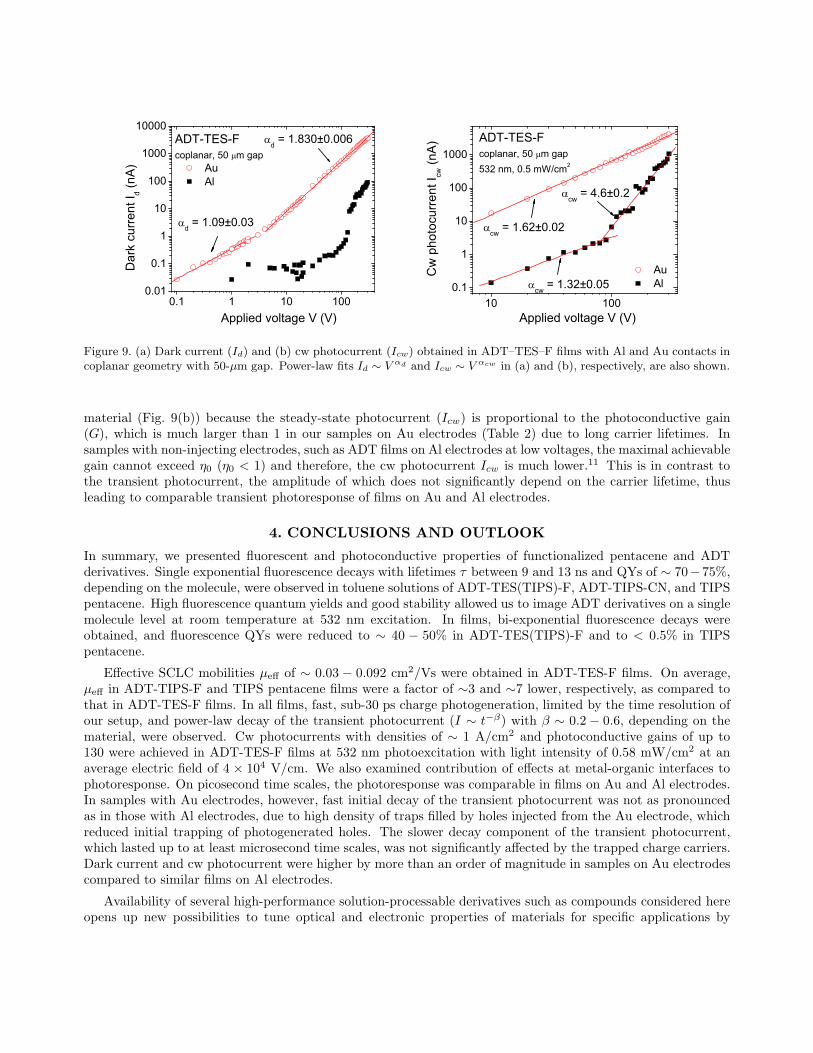
Dark current and cw photocurrent Unlike the amplitudes of transient photocurrent, the cw photocurrents(Icw) and dark currents (Id) for films on Au and on Al electrodes differed by more than an order of magnitudeover a wide range of applied voltages, with much higher currents measured in samples with Au electrodes(Fig. 9). Voltage dependencies of the dark current and of the cw photocurrent observed in samples with Auand Al electrodes were drastically different, indicative of different mechanisms responsible for observed currents,depending on the electrode material. In samples with Au electrodes, the relationship between dark currentand voltage (Id ∼ V αd) was close to linear at very low voltages and close to quadratic at higher voltages (e.g.αd = 1.09±0.03 at voltages below 2 V and 1.830±0.006 from 2 to 300 V in an ADT–TES–F film in Fig. 9(a)). Incontrast, in samples with Al electrodes, dark current was weakly voltage-dependent at lower voltages, followedby a steep increase at higher voltages. Despite this sharp increase, even at the highest applied voltage of 300 Vused in our experiments, dark current in samples with Al electrodes was much lower than that in samples withAu electrodes at the same voltage. In films on either Au or Al electrodes, the cw photocurrent was higher thanthe dark current in the entire range of light intensities used. Regardless of the material, in samples with Auelectrodes, αcw obtained from the fit of voltage dependence of the photocurrent (Icw ∼ V αcw ) ranged between1.5 and 2.2, depending on the sample. In any given sample, however, a single value of αcw was sufficient todescribe voltage dependence of the cw photocurrent over a large voltage range (e.g. αcw = 1.62±0.02 from 0.5to 100 V in an ADT–TES–F film in Fig. 9(b)). In samples with Al electrodes, however, αcw was ∼1.3–3 at lowervoltages (e.g. αcw = 1.32±0.05 in Fig. 9(b)), depending on the sample, followed by steep transition described byαcw ∼3.3–5 (e.g. αcw = 4.6±0.2 in Fig. 9(b)) at higher voltages. Similar trends were observed in ADT–TIPS–Ffilms.11
The photoresponse under cw illumination is strongly affected by the conditions imposed by the electrode
0.1 1 10 1000.01
0.1
1
10
100
1000
10000
Au Al
d = 1.830±0.006D
ark
curr
ent I
d (nA
)
Applied voltage V (V)
d = 1.09±0.03
ADT-TES-Fcoplanar, 50 m gap
10 1000.1
1
10
100
1000
Applied voltage V (V)
Cw
pho
tocu
rren
t Icw
(nA
)
cw = 4.6±0.2
cw = 1.62±0.02
Au Al
cw = 1.32±0.05
ADT-TES-Fcoplanar, 50 m gap532 nm, 0.5 mW/cm2
Figure 9. (a) Dark current (Id) and (b) cw photocurrent (Icw) obtained in ADT–TES–F films with Al and Au contacts incoplanar geometry with 50-µm gap. Power-law fits Id ∼ V αd and Icw ∼ V αcw in (a) and (b), respectively, are also shown.
material (Fig. 9(b)) because the steady-state photocurrent (Icw) is proportional to the photoconductive gain(G), which is much larger than 1 in our samples on Au electrodes (Table 2) due to long carrier lifetimes. Insamples with non-injecting electrodes, such as ADT films on Al electrodes at low voltages, the maximal achievablegain cannot exceed η0 (η0 < 1) and therefore, the cw photocurrent Icw is much lower.11 This is in contrast tothe transient photocurrent, the amplitude of which does not significantly depend on the carrier lifetime, thusleading to comparable transient photoresponse of films on Au and Al electrodes.
4. CONCLUSIONS AND OUTLOOK
In summary, we presented fluorescent and photoconductive properties of functionalized pentacene and ADTderivatives. Single exponential fluorescence decays with lifetimes τ between 9 and 13 ns and QYs of ∼ 70−75%,depending on the molecule, were observed in toluene solutions of ADT-TES(TIPS)-F, ADT-TIPS-CN, and TIPSpentacene. High fluorescence quantum yields and good stability allowed us to image ADT derivatives on a singlemolecule level at room temperature at 532 nm excitation. In films, bi-exponential fluorescence decays wereobtained, and fluorescence QYs were reduced to ∼ 40 − 50% in ADT-TES(TIPS)-F and to < 0.5% in TIPSpentacene.
Effective SCLC mobilities µeff of ∼ 0.03 − 0.092 cm2/Vs were obtained in ADT-TES-F films. On average,µeff in ADT-TIPS-F and TIPS pentacene films were a factor of ∼3 and ∼7 lower, respectively, as compared tothat in ADT-TES-F films. In all films, fast, sub-30 ps charge photogeneration, limited by the time resolution ofour setup, and power-law decay of the transient photocurrent (I ∼ t−β) with β ∼ 0.2 − 0.6, depending on thematerial, were observed. Cw photocurrents with densities of ∼ 1 A/cm2 and photoconductive gains of up to130 were achieved in ADT-TES-F films at 532 nm photoexcitation with light intensity of 0.58 mW/cm2 at anaverage electric field of 4 × 10⁴ V/cm. We also examined contribution of effects at metal-organic interfaces tophotoresponse. On picosecond time scales, the photoresponse was comparable in films on Au and Al electrodes.In samples with Au electrodes, however, fast initial decay of the transient photocurrent was not as pronouncedas in those with Al electrodes, due to high density of traps filled by holes injected from the Au electrode, whichreduced initial trapping of photogenerated holes. The slower decay component of the transient photocurrent,which lasted up to at least microsecond time scales, was not significantly affected by the trapped charge carriers.Dark current and cw photocurrent were higher by more than an order of magnitude in samples on Au electrodescompared to similar films on Al electrodes.
Availability of several high-performance solution-processable derivatives such as compounds considered hereopens up new possibilities to tune optical and electronic properties of materials for specific applications by
creating mixtures of various derivatives.21, 24 Our ability to image ADT derivatives on a single molecule levelrepresents an exciting development that allows us to study charge- and energy transfer on a molecular level. Thisenables comparison between molecular properties and those of bulk films in technologically relevant materials.These studies are currently underway.
5. ACKNOWLEDGEMENTS
This work was supported in part by the Petroleum Research Fund, Office of Naval Research (grant #N00014-07-1-0457 via ONAMI Nanometrology and Nanoelectronics Initiative), and National Science Foundation viaCAREER program (DMR-0748671).
REFERENCES
[1] Forrest, S. R., “The path to ubiquitous and low-cost organic electronic appliances on plastic,” Nature 428,911 (2004).
[2] Murphy, A. R. and Frechet, J. M. J., “Organic semiconducting oligomers for use in thin film transistors,”Chem. Rev. 107, 1066–1096 (2007).
[3] Geffroy, B., le Roy, P., and Prat, C., “Organic light-emitting diode (OLED) technology: materials, devicesand display technologies,” Poly. Int. 55, 572–582 (2006).
[4] Ostroverkhova, O. and Moerner, W. E., “Organic photorefractives: mechanisms, materials and applica-tions,” Chem. Rev. 104(7), 3267–3314 (2004).
[5] Anthony, J. E., “Functionalized acenes and heteroacenes for organic electronics,” Chem. Rev. 106, 5028–5048 (2006).
[6] Park, S. K., Mourey, D. A., Subramanian, S., Anthony, J. E., and Jackson, T. N., “High-mobility spin-castorganic thin film transistors,” Appl. Phys. Lett. 93, 043301 (2008).
[7] Gundlach, D. J., Royer, J. E., Park, S. K., Subramanian, S., Jurchescu, O. D., Hamadani, B. H., Moad,A. J., Kline, R. J., Teague, L. C., Kirillov, O., Richter, C. A., Kushmerick, J. G., Richter, L. J., Parkin,S. R., Jackson, T. N., and Anthony, J. E., “Contact-induced crystallinity for high-performance solubleacene-based transistors and circuits,” Nat. Mat. 7, 216 (Mar. 2008).
[8] Ostroverkhova, O., Cooke, D. G., Shcherbyna, S., R. F. Egerton, R. F., Hegmann, F. A., Tykwinski, R. R.,and Anthony, J. E., “Band-like transport in pentacene and functionalized pentacene thin films revealed bytransient photoconductivity,” Phys. Rev. B 71, 035204 (2005).
[9] Ostroverkhova, O., Shcherbyna, S., Cooke, D. G., Egerton, R. F., Hegmann, F. A., Tykwinski, R. R.,Parkin, S. R., and Anthony, J. E., “Optical and transient photoconductive properties of pentacene andfunctionalized pentacene thin films: Dependence on film morphology,” J. Appl. Phys. 98, 033701 (2005).
[10] Day, J., Subramanian, S., Anthony, J. E., Lu, Z., Twieg, R. J., and Ostroverkhova, O., “Photoconductivityin organic thin films: From picoseconds to seconds after excitation,” J. Appl. Phys. 103, 123715 (2008).
[11] Day, J., Platt, A. D., Subramanian, S., Anthony, J. E., and Ostroverkhova, O., “Influence of organicsemiconductor-metal interfaces on the photoresponse of functionalized anthradithiophene thin films,” J.
Appl. Phys. 105, 103703 (2009).
[12] Lehnherr, D., Gao, J., Hegmann, F. A., and Tykwinski, R. R., “Synthesis and electronic properties ofconjugated pentacene dimers,” Org. Lett. 10(21), 4779–4782 (2008).
[13] Gao, J. and Hegmann, F. A., “Bulk photoconductive gain in pentacene,” Appl. Phys. Lett. 93, 223306(2008).
[14] Wolak, M. A., Delcamp, J., Landis, C. A., Lane, P. A., Anthony, J., and Kafafi, Z., “High-performanceorganic light-emitting diodes based on dioxolane-substituted pentacene derivatives,” Adv. Funct. Mat. 16,1943–1949 (2006).
[15] Platt, A. D., Day, J., Subramanian, S., Anthony, J. E., and Ostroverkhova, O., “Optical, fluorescent, and(photo)conductive properties of high-performance functionalized pentacene and anthradithiophene deriva-tives,” J. Phys. Chem. C (In Press).
[16] Park, S. K., Jackson, T. N., Anthony, J. E., and Mourey, D. A., “High mobility solution processed 6,13-bis(triisopropyl-silylethynyl) pentacene organic thin film transistors,” Appl. Phys. Lett. 91, 063514 (2007).
[17] Subramanian, S., Park, S. K., Parkin, S. R., Podzorov, V., Jackson, T. N., and Anthony, J. E., “Chro-mophore flourination enhances crystallization and stability of soluble anthradithiophene semiconductors,”J. Am. Chem. Soc. 130, 2706 (2008).
[18] Lakowicz, J. R., [Principles of Fluorescence Spectroscopy ], Springer, New York (2006).
[19] Lord, S. J., Lu, Z., Wang, H., Willets, K. A., Schuck, P. J., Lee, H.-l. D., Nishimura, S. Y., Twieg, R. J., andMoerner, W. E., “Photophysical properties of acene DCDHF fluorophores: Long-wavelength single-moleculeemitters designed for cellular imaging,” J. Phys. Chem. A 111, 8934–8941 (2007).
[20] Haugland, R. P., ed., [The Handbook: A Guide to Fluorescent Probes and Labeling Technologies ], MolecularProbes, Eugene, OR, 10 ed. (2005).
[21] Day, J., Platt, A. D., Ostroverkhova, O., Subramanian, S., and Anthony, J. E., “Organic semiconductorcomposites: influence of additives on the transient photocurrent,” Appl. Phys. Lett. 94, 013306 (2009).
[22] Coppo, P. and Yeates, S. G., “Shining Light on a Pentacene Derivative: The Role of Photoinduced Cy-cloadditions,” Adv. Mat. 17, 3001–3005 (2005).
[23] Bassler, H. and Schweitzer, B., “Site-selective fluorescence spectroscopy of conjugated polymers andoligomers,” Acc. Chem. Res. 32, 173–182 (1999).
[24] Platt, A. D., Shepherd, W. E. B., Anthony, J. E., and Ostroverkhova, O., “Photophysical and photocon-ductive properties of organic semiconductor composites,” Proc. SPIE 7413 (2009).
[25] Pope, M. and Swenberg, C. E., [Electronic Processes in Organic Crystals ], Oxford University Press, NewYork (1982).
[26] Como, E. D., Loi, M. A., Murgia, M., Zamboni, R., and Muccini, M., “J-aggregation in α-sexithiophenesubmonolayer films on silicon dioxide,” J. Am. Chem. Soc. 128, 4277–4281 (2006).
[27] der Auweraer, M. V. and Scheblykin, I., “One-dimensional J-aggregates: Dependence of the properties ofthe exciton band on the model of the intermolecular coupling,” Chem. Phys. 275, 285–306 (2002).
[28] Spano, F. C., “Temperature dependent exciton emission from herringbone aggregates of conjugatedoligomers,” J. Chem. Phys. 120, 7643–7658 (2004).
[29] Platt, A. D., Day, J., Shepherd, W. E., and Ostroverkhova, O., “Photophysical and photoconductive prop-erties of novel organic semiconductors,” in [ACS Organic Thin Films for Photonic Applications ], AmericanChemical Society, Washington D.C. (2009).
[30] Ostroverkhova, O., Cooke, D. G., Hegmann, F. A., Anthony, J. E., Podzorov, V., Gershenson, M. E.,Jurchescu, O. D., and Palstra, T. T. M., “Ultrafast carrier dynamics in pentacene, functionalized pentacene,tetracene and rubrene single crystals,” Appl. Phys. Lett. 88, 162101 (2006).
[31] Moses, D., Soci, C., Chi, X., and Ramirez, A. P., “Mechanism of carrier photogeneration and carriertransport in molecular crystal tetracene,” Phys. Rev. Lett. 97, 067401 (2006).
[32] Hu, W., Pflaum, J., Schweitzer, D., and Dressel, M., “Transport properties of [2,2]-paracyclophane thinfilms,” Appl. Phys. Lett. 84, 4720–4722 (2004).
[33] Day, J., Platt, A. D., Subramanian, S., Anthony, J. E., and Ostroverkhova, O., “Influence of organicsemiconductor-metal interfaces on the photoresponse of functionalized anthradithiophene thin films,” J.
Appl. Phys. 105, 103703 (2009).
[34] Jurchescu, O. D., Subramanian, S., Kline, R. J., Hudson, S. D., Anthony, J. E., Jackson, T. N., andGundlach, D. J., “Organic single-crystal field-effect transistors of a soluble anthradithiophene,” Chem.
Mat. 20(21), 6733–6737 (2008).
[35] Lee, C., Yu, G., Moses, D., Pakbaz, K., Zhang, C., Sariciftci, N. S., Heeger, A. J., and Wudl, F., “Sensi-tization of the photoconductivity of conducting polymers by C60: Photoinduced electron transfer,” Phys.
Rev. B 48, 15425 (1993).
[36] Godlewski, J., Jarosz, G., and Signerski, R., “Photoenhanced current in thin organic layers,” Appl. Surf.
Sci. 175–176, 344–350 (2001).
[37] Itaka, K., Myojin, N., Yamashiro, M., Yamaguchi, J., and Koinuma, H., “Molecular beam epitaxy of highlyoriented pentacene thin films on an atomically flat sapphire substrate,” Jap. J. Appl. Phys. 44, 6249–6251(2005).