Embed Size (px)
Citation preview
OPTI510R: Photonics
Khanh Kieu
College of Optical Sciences,
University of Arizona
Meinel building R.626
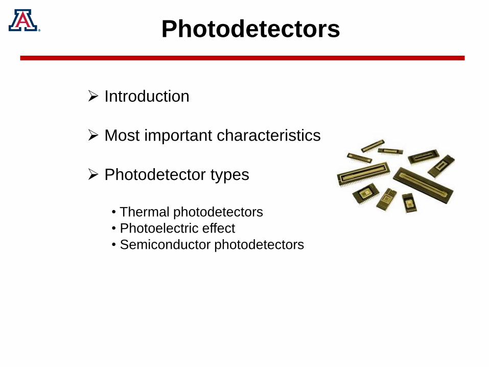
Photodetectors
Introduction
Most important characteristics
Photodetector types
• Thermal photodetectors
• Photoelectric effect
• Semiconductor photodetectors

Photodetectors
p-n photodiode
Response time
p-i-n photodiode
APD photodiode
Noise
Wiring
Arrayed detector (Home Reading)
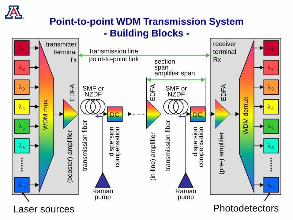
l1
l2
l3
l4
l5
l6
ln
WD
M m
ux
l1
l2
l3
l4
l5
l6
ln
WD
M d
em
ux
(booste
r) a
mplif
ier
transmitter
terminal
Tx
receiver
terminal
Rx
(pre
-) a
mplif
ier
(in
-lin
e)
am
plif
ier
ED
FA
ED
FA
ED
FA
transm
issio
n fib
er
transm
issio
n fib
er
dis
pers
ion
com
pen
sation
dis
pers
ion
com
pen
sation
DC DC
Ramanpump
Ramanpump
sectionspanamplifier span
transmission line
point-to-point link
SMF orNZDF
SMF orNZDF
Point-to-point WDM Transmission System
- Building Blocks -
Laser sources Photodetectors

Introduction
Convert optical data into
electrical data
Laser beam characterization
• Power measurement
• Pulse energy measurement
• Temporal waveform measurement
• Beam profile
Introduction
Photodetector converts photon energy to a signal, mostly
electric signal such as current (sort of a reverse LED)
Photoelectric detector
• Carrier generation by incident light
• Carrier transport and/or multiplication by current gain mechanism
• Interaction of current with external circuit
Thermal detector
• Conversion of photon to phonon (heat)
• Propagation of phonon
• Detection of phonon

Important characteristics
Wavelength coverage
Sensitivity
Bandwidth (response time)
Noise
Surface area
Reliability
Cost
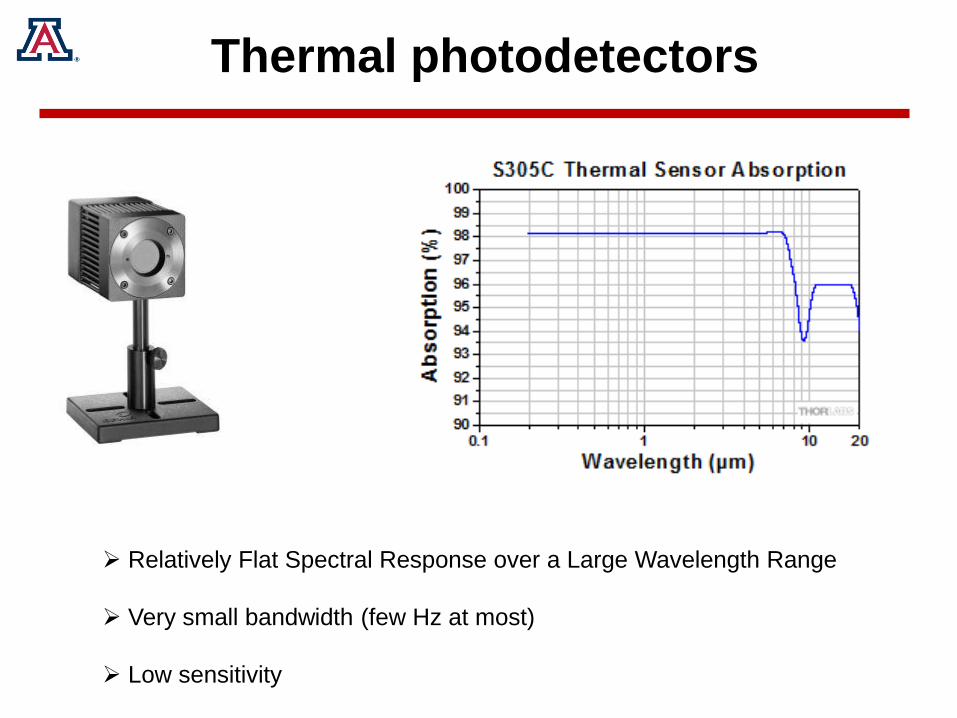
Thermal photodetectors
Relatively Flat Spectral Response over a Large Wavelength Range
Very small bandwidth (few Hz at most)
Low sensitivity

Thermal photodetectors
Standard thermal power meters

Photoelectric effect
Absorption of photons creates carriers (electrons)
• External photoeffect: electron escape from materials
as free electrons
• Internal photoeffect (photoconductivity): excited
carriers remain within the material to increase
conductivity
Useful formula:
)(
24.1)(
eVEm
g
l

Photoelectric Effect
• Electrons were emitted immediately, no time lag.
• Increasing intensity of light increased number of photoelectrons but not their
maximum kinetic energy.
• Red light will not cause ejection of electrons, no matter what the intensity (linear
regime).
• A weak violet light will eject only a few electron, but their maximum kinetic
energies are greater than those for intense light of longer wavelength.
Photoelectric effect :
a photon with a minimum
energy is absorbed to
create a free electron..EKWh

Photoelectric Effect
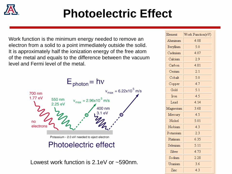
Photoelectric Effect
Work function is the minimum energy needed to remove an
electron from a solid to a point immediately outside the solid.
It is approximately half the ionization energy of the free atom
of the metal and equals to the difference between the vacuum
level and Fermi level of the metal.
Lowest work function is 2.1eV or ~590nm.

Photo-multiplier tubes (PMT)
Vacuum photodiode operates when a photon creates a free electron at
the photocathode, which travels to the anode, creating a photocurrent.
Photocathode can be opaque (reflection mode) or semitransparent
(transmission mode).
Original electron can create secondary electrons using dynodes, with
successive higher potentials, such as a photomultiplier tube, PMT.

Photomultiplier tubes typically require 1000 to 2000 volts for proper operation. The
most negative voltage is connected to the cathode, and the most positive voltage is
connected to the anode. Voltages are distributed to the dynodes by a resistive
voltage divider, though variations such as active designs (with transistors or diodes)
are possible.
Photo-multiplier tubes (PMT)

Photo-multiplier tubes (PMT)
Ag-O-Cs: The transmission-mode photocathode using this material is designated
S-1 and sensitive from the visible to infrared range (300 to 1200nm). Ag-O-Cs has
comparatively high thermionic dark emission.
GaAs(Cs): GaAs activated in cesium is also used as a photocathode. The spectral
response of this photocathode usually covers a wider spectral response range
from ultraviolet to 930nm.
InGaAs(Cs): This photocathode has greater extended sensitivity in the infrared
range than GaAs. Moreover, in the range between 900 and 1000nm, InGaAs has
much higher S/N ratio than Ag-O-Cs.
Sb-Cs: This is a widely used photocathode and has a spectral response in the
ultraviolet to visible range. This is not suited for transmission-mode photocathodes
and mainly used for reflection-mode photocathodes.
Bialkali (Sb-Rb-Cs, Sb-K-Cs): These have a spectral response range similar to
the Sb-Cs photocathode, but have higher sensitivity and lower noise than Sb-Cs.

Photo-multiplier tubes (PMT)

Photo-multiplier tubes (PMT)
With internal amplifier
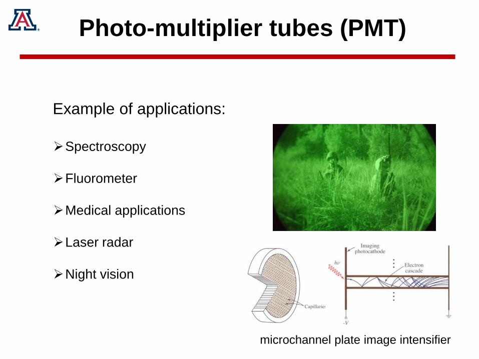
Photo-multiplier tubes (PMT)
Spectroscopy
Fluorometer
Medical applications
Laser radar
Night vision
Example of applications:
microchannel plate image intensifier

Photoelectric Effect
Maximum kinetic energy from a metal: WhE max
Maximum kinetic energy from a semiconductor: )(max gEhE
= electron affinity, difference between vacuum level and bottom of conduction band

Negative electron affinity
• Semiconductor with conduction band edge above vacuum
level
• Photon with E > Eg creates free electrons
• III-V semiconductor (ex. GaAs) can be activated to a state
of negative electron affinity by treatment of surface with
cesium and oxygen

Internal photoelectric effect
1) Generation: photons are converted to free carriers
2) Transport: applied E field moves the free carriers
3) Gain: accelerated carriers create more carriers by impact
ionizations (in APD, for example)
Most photodetectors operate on photoconductivity, where carriers are
generated inside the crystal. One example is the photodiode based on a p-n
junction. Gain can be achieved through impact ionization by initial electrons.
Amplified photoelectric detectors involve three processes:

Quantum efficiency
Quantum efficiency, h, equals to probability of single photon to
generate a pair of detectable carriers
)exp(1)1( dR h
fraction of e-h contribute to current
surface reflectionfraction of absorbed photons
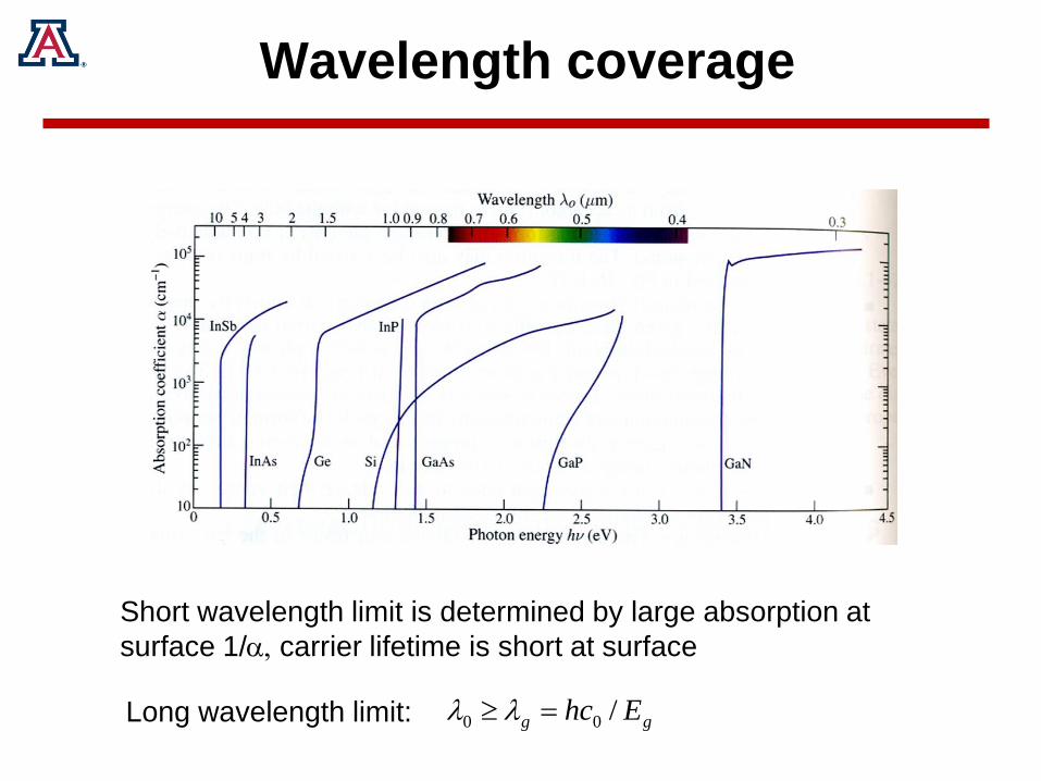
Wavelength coverage
gg Ehc /00 llLong wavelength limit:
Short wavelength limit is determined by large absorption at
surface 1/, carrier lifetime is short at surface

Responsivity
Responsivity, R, relates electric current, ip, and incident optical power P
RPh
ePip
h
)/(24.1
)(0 WattAmpm
h
eR
lh
h
For h=1, l=1.24m, R=1 (A/W)
We consider here linear
response only. All detectors
saturate at high power and
have finite dynamic range.
Responsivity
24.1
paircarrier per generated charge of #
0lh
h
GR
h
ePGi
eG
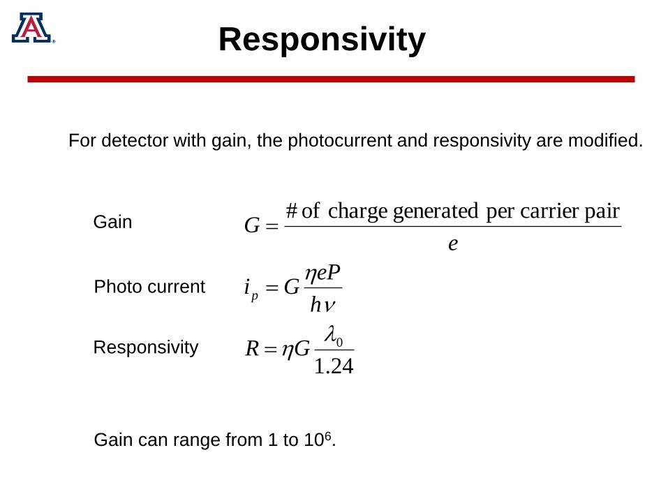
p
For detector with gain, the photocurrent and responsivity are modified.
Gain
Photo current
Responsivity
Gain can range from 1 to 106.
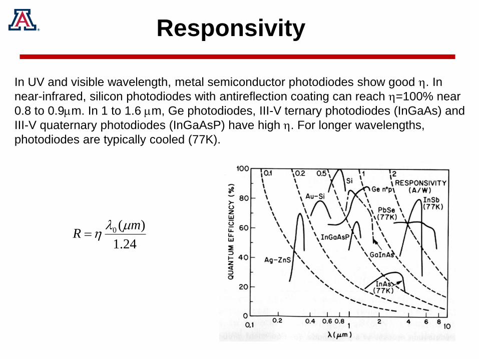
Responsivity
24.1
)(0 mR
lh
In UV and visible wavelength, metal semiconductor photodiodes show good h. In
near-infrared, silicon photodiodes with antireflection coating can reach h=100% near
0.8 to 0.9m. In 1 to 1.6 m, Ge photodiodes, III-V ternary photodiodes (InGaAs) and
III-V quaternary photodiodes (InGaAsP) have high h. For longer wavelengths,
photodiodes are typically cooled (77K).

Response time: Ramo’s theorem
Em
eEav colcol
Vdttidxw
VQQEdx )()(
Even if the photon is absorbed instantaneously with the generation of e-h pair,
there is a finite time before the carriers emerge as a detectable current.
In a constant electric field, E, inside a semiconductor, charge carriers will (1)
accelerate with acceleration, a, (2) collide with imperfection and (3) effectively
travel with an average velocity, .
Here col is mean time between collision and m is effective mass, is mobility.
Consider a carrier with charge Q moves a distance dx in time dt under a field E=V/w
By energy conservation:
)()( tvw
Q
dt
dx
w
Qti
A carrier moving with a drift velocity in x direction
creates a current
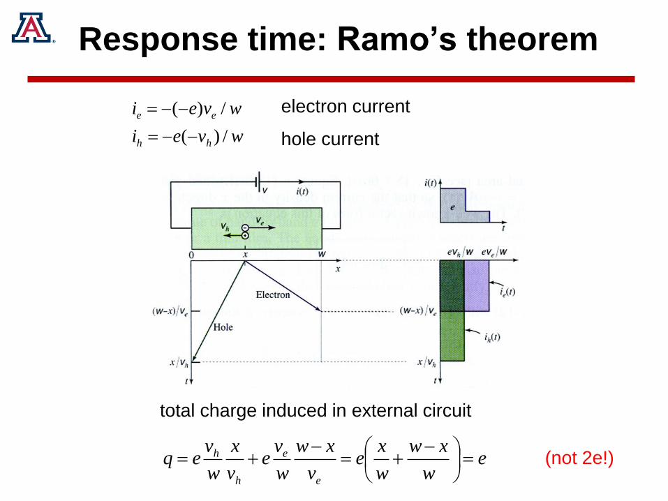
Response time: Ramo’s theorem
wvei
wvei
hh
ee
/)(
/)(
electron current
hole current
ew
xw
w
xe
v
xw
w
ve
v
x
w
veq
e
e
h
h
total charge induced in external circuit
(not 2e!)

Response time: Ramo’s theorem
elsewhere0
0,)( 2
2
h
hh
h v
wt
w
Nevt
w
Nev
ti
Current for each type of carrier is linear with time. Charge delivered to external
circuit is not instantaneous and has a finite spread determined by drift velocities.
Current induced by N photons uniformly distributed between 0 and w. i(t) can be
viewed as the impulse response function for a uniformly illuminated detector subject
to transit time spread.

Photoconductors
Photoconductive detectors can be classified as intrinsic or extrinsic. In intrinsic
photoconductor, mobile charge carriers are generated by incident photon flux F
(photon per second). The generated photo-current is proportional to the photon flux:
is the excess carrier recombination lifetime
e is the electron transit time
(interdigitated electrodes to maximize light collection and minimize transit time)

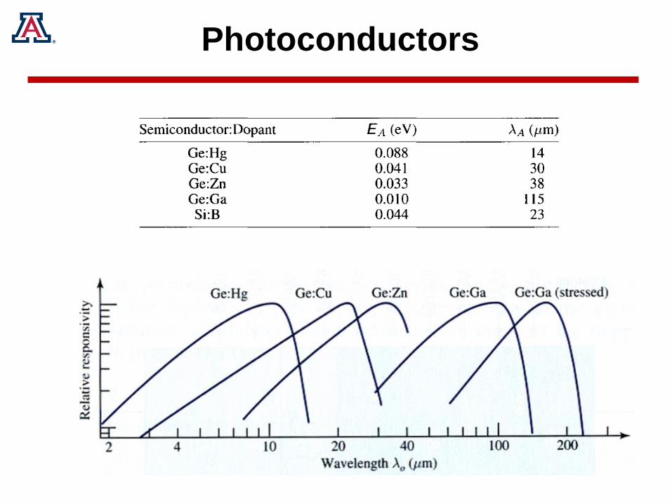
Photoconductors
Photoconducivity can be achieved in longer wavelengths by using dopant.
Incident photons can interact with electron at a donor site, creating a free electron
or with a bound hole at an acceptor site, creating a free hole. Donor and acceptor
levels are characterized by the activation energy (EA) and wavelength (lA).
A
AE
hc0l
Photoconductors

Quantum well photodetectors
640 x 512 pixels focal plane array
Photoconductive detectors can be constructed using multiple quantum wells.
In a quantum well infrared photodetector (QWIP), an incident infrared photon
releases an electron occupying a bound energy level in a quantum well,
creating a free carrier.
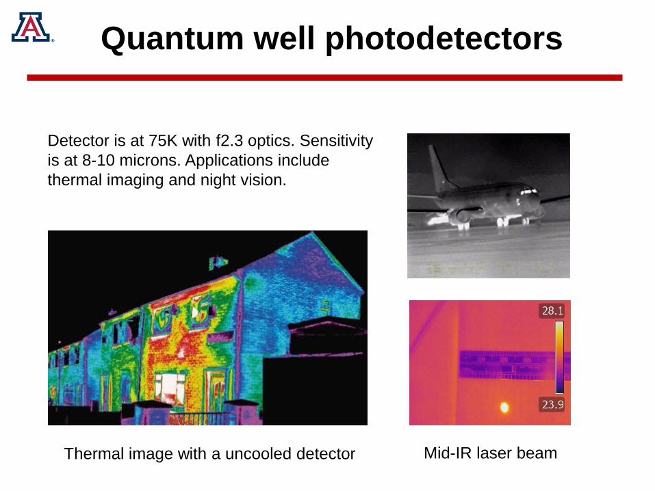
Quantum well photodetectors
Detector is at 75K with f2.3 optics. Sensitivity
is at 8-10 microns. Applications include
thermal imaging and night vision.
Thermal image with a uncooled detector Mid-IR laser beam


![· Indicator, IP 40 Product can differ from the current configuration. Dimensions [mm] H = Universal terminal 2.0 x 0.5 mm, L = Solder terminal, L1 = Solder terminal 2.8 x 0.5 mm](https://img.pdfslide.us/doc/110x75/5ea10d0f19728302e976ebe0/indicator-ip-40-product-can-differ-from-the-current-configuration-dimensions-mm.jpg)