Embed Size (px)
Citation preview

Stanford University
Center for Integrated Systems 2004.10.05 Department of Electrical Engineering
Silicon Devices at the “End of Scaling” –Opportunities and Challenges
H.-S. Philip WongProfessor of Electrical Engineering Stanford University, Stanford, California, [email protected]
http://www.stanford.edu/~hspwong
Stanford University
Department of Electrical Engineering2 H-.S. Philip Wong 2004.10.05
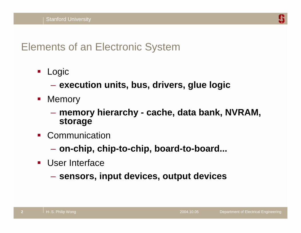
Elements of an Electronic System
! Logic– execution units, bus, drivers, glue logic
! Memory– memory hierarchy - cache, data bank, NVRAM,
storage! Communication
– on-chip, chip-to-chip, board-to-board...! User Interface
– sensors, input devices, output devices

Stanford University
Department of Electrical Engineering3 H-.S. Philip Wong 2004.10.05
What is Classical Scaling?! Scaling is the synchronous reduction, year on year, of technology dimensions
governing the performance of silicon technology. Scaling;– Improves device performance at ever lower power per function.– Enables increased chip functionality through added density.– Improves business financials through die size reduction.
! Why would the end of classical scaling be a highly disruptive event?– Scaling and progress in silicon technology have been synonymous for decades.
p substrate, doping αααα*N A
Scaled Device
L/αααα xd/αααα
GATEn+ source
n+ drain
W IRINGVoltage, V / αααα
W /ααααtox/αααα
SCALING:Voltage: V/αOxide: tox /αWire width: W/αGate width: L/αDiffusion: xd /αSubstrate: α * NA
RESULTS:Higher Density: ~α2
Higher Speed: ~αPower/ckt: ~1/α2
Power Density: ~Constant
Source: IBM

Stanford University
Department of Electrical Engineering4 H-.S. Philip Wong 2004.10.05
SCALING:Voltage: V/αOxide: tox /αWire width: W/αGate width: L/αDiffusion: xd /αSubstrate: α * NA
RESULTS:Higher Density: ~α2
Higher Speed: ~αPower/ckt: ~1/α2
Power Density: ~Constant
"Why deviate from "ideal" scaling"unacceptable gate leakage/reliability"additional performance at higher voltages
"What is the consequence of this deviation?"a dramatic rise in power density
p substrate, doping αααα*NA
Scaled Device
L/αααα xd/αααα
GATEn+ source
n+ drain
WIRINGVoltage, V / αααα
W/ααααtox/αααα
0.01 0.1 1Gate Length, Lgate (um)
0.1
1
10
100
1000
classic scaling
Tox (C)
Vdd (V)
Vt (V)
Some Things do not Scale Exactly…
Source: IBM

Stanford University
Department of Electrical Engineering5 H-.S. Philip Wong 2004.10.05
Active vs. Passive Power
0.010.110.001
0.01
0.1
1
10
100
1000
Gate Length (microns)
Active Power
Passive Power
1994 2004
Pow
er D
ensi
ty (W
/cm
2 )
! Power components:– Active power
– Passive power• Gate leakage• Sub-threshold
leakage (source-drain leakage)
10S Tox=11AGate Stack
Gate dielectric approaching a fundamental limit (a few atomic layers)
Source: IBM
Stanford University
Department of Electrical Engineering6 H-.S. Philip Wong 2004.10.05
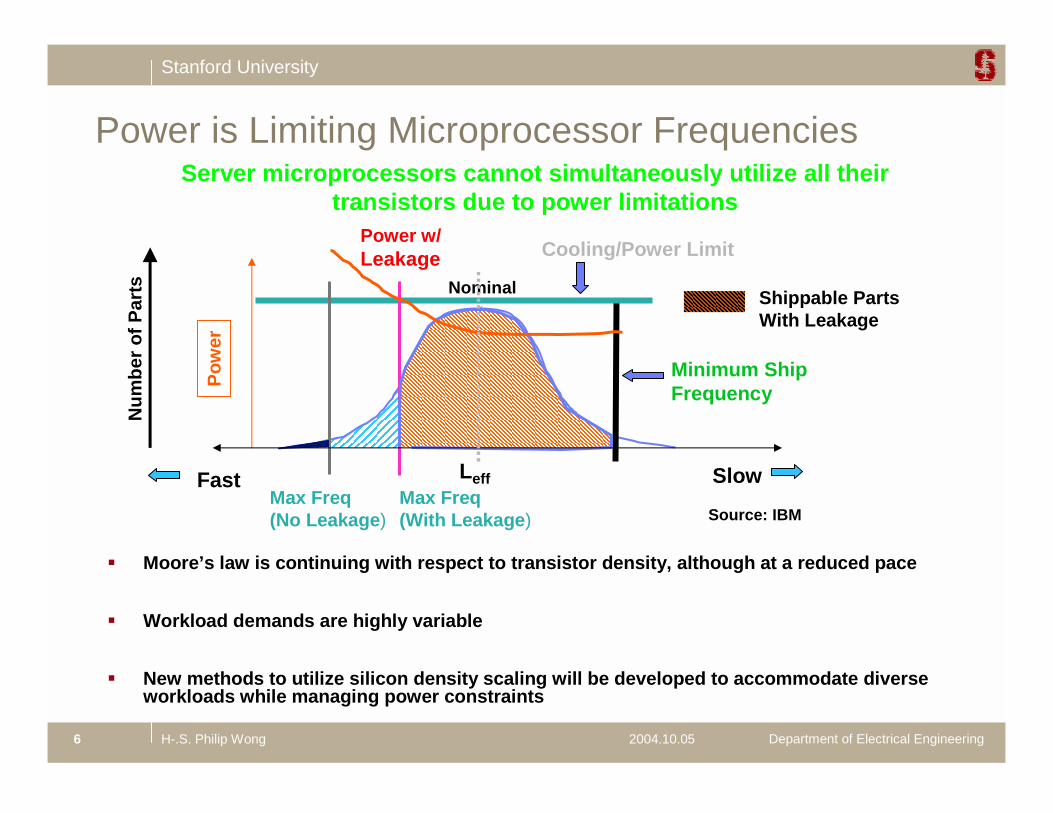
Power is Limiting Microprocessor Frequencies
! Moore’s law is continuing with respect to transistor density, although at a reduced pace
! Workload demands are highly variable
! New methods to utilize silicon density scaling will be developed to accommodate diverse workloads while managing power constraints
Server microprocessors cannot simultaneously utilize all their transistors due to power limitations
Shippable PartsWith Leakage
Minimum Ship Frequency
Leff SlowFast
Nominal
Pow
er
Cooling/Power Limit
Max Freq(No Leakage)
Max Freq(With Leakage)
Power w/Leakage
Num
ber o
f Par
ts
Source: IBM

Stanford University
Department of Electrical Engineering7 H-.S. Philip Wong 2004.10.05
Key Challenges
! Power / performance improvement and optimization
! Variability
! Integration– Device, circuit, system

Stanford University
Department of Electrical Engineering8 H-.S. Philip Wong 2004.10.05
Let’s start with logic devices

Stanford University
Department of Electrical Engineering9 H-.S. Philip Wong 2004.10.05
Improvement OpportunitiesTh
resh
old
Volta
ge (V
T)
Gate Length (LG)
Thin gate dielectric
Doping: sharp halo & junction profiles
Thin silicon body
Innovations:
! materials
! device structure
well doping depletion layer
isolationburied oxide
halo
Silicon Substrate
raised source/drain channel
Gate length scaling

Stanford University
Department of Electrical Engineering10 H-.S. Philip Wong 2004.10.05
Improvement Opportunities
Drain Voltage (VDS)
Dra
in C
urre
nt (I
D)
Contact & series resistance
Mobility
MobilitySaturation velocityBallistic transport
Charge density: subthreshold slope
Innovations:
! materials
! device structure
Dra
in C
urre
nt (l
og(I D
))
Gate Voltage (VGS)
Dra
in C
urre
nt (I
D)
Stanford University
Department of Electrical Engineering11 H-.S. Philip Wong 2004.10.05
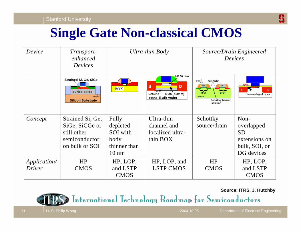
Device Transport-enhanced Devices
Ultra-thin Body Source/Drain Engineered Devices
Concept Strained Si, Ge, SiGe, SiCGe or still other semiconductor; on bulk or SOI
Fully depleted SOI with body thinner than 10 nm
Ultra-thin channel and localized ultra-thin BOX
Schottky source/drain
Non-overlapped SD extensions on bulk, SOI, or DG devices
Application/Driver
HP CMOS
HP, LOP, and LSTP
CMOS
HP, LOP, and LSTP CMOS
HP CMOS
HP, LOP, and LSTP
CMOS
Strained Si, Ge, SiGe
isolation
buried oxide
Silicon Substrate
BOX
Bulk wafer BOX (<20nm)
S D GroundPlane
FD Si film Gate
Schottky barrierisolation
Silicon
silicideGate
{{ {{
nFET
{{ {{
pFET
Bias
Non-overlapped region S D
Single Gate Non-classical CMOS
Source: ITRS, J. Hutchby

Stanford University
Department of Electrical Engineering12 H-.S. Philip Wong 2004.10.05
Device Multiple Gate FET
N-Gate (N>2) FET
Double-gate FET
Concept Tied gates (number of channels >2)
Tied gates, side-wall conduction
Tied gates planar conduction
Independently switched gates, planar conduction
Vertical conduction
Application/Driver HP, LOP, and LSTP CMOS
HP, LOP, and LSTP CMOS
HP, LOP, and LSTP CMOS
LOP and LSTP CMOS
HP, LOP, and LSTP CMOS
Source Drain
Gate
Source Drain
Gate
Source Drain
Gate
STI
n+
Si-substrate
SOURCE
GATE
DRAIN
n+
STI
n+
Si-substrate
SOURCE
GATE
DRAIN
n+
Multiple Gate Non-classical CMOS
Source: ITRS, J. Hutchby
Stanford University
Department of Electrical Engineering13 H-.S. Philip Wong 2004.10.05
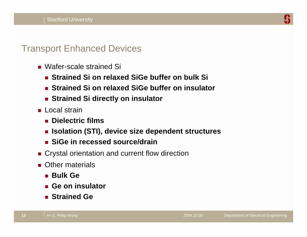
Transport Enhanced Devices
# Wafer-scale strained Si# Strained Si on relaxed SiGe buffer on bulk Si# Strained Si on relaxed SiGe buffer on insulator# Strained Si directly on insulator
# Local strain# Dielectric films# Isolation (STI), device size dependent structures# SiGe in recessed source/drain
# Crystal orientation and current flow direction# Other materials
# Bulk Ge# Ge on insulator# Strained Ge

Stanford University
Department of Electrical Engineering14 H-.S. Philip Wong 2004.10.05
Strained Silicon
Strained Si/SiGeBulk MOSFET
Strained SiStrained SiStrained SiStrained Si
Relaxed SiGeRelaxed SiGeRelaxed SiGeRelaxed SiGe
SGOI (SiGe-on-Insulator) MOSFET
Strained SiStrained SiStrained SiStrained Si
Buried OxideBuried OxideBuried OxideBuried Oxide
Relaxed SiGeRelaxed SiGeRelaxed SiGeRelaxed SiGe
SSDOI MOSFET
Strained SiStrained SiStrained SiStrained Si
Buried OxideBuried OxideBuried OxideBuried Oxide
Buried Oxide
SSDOI 16 nm
Silicide onselective epi
K. Rim et al., IEDM, 2003.K. Rim et al., Symp. VLSI Tech., p. 59, 2001.
Relaxed SiGe
Strained SiChannel
Co salicideformed onraised S/D
K. Rim et al., Symp. VLSI Tech., p. 98, 2002.
60nm
Buried oxide
Strained silicon
SiGe
CoSi2 on RSD
B. Lee et al., IEDM 2002

Stanford University
Department of Electrical Engineering15 H-.S. Philip Wong 2004.10.05
Strain-Dependence of Mobility
! Mobility enhancements consistent with amount of strain even for strained silicon on insulator
0 10 20 30 40 50
1.0
1.5
2.0
2.50.0 0.5 1.0 1.5 2.0
Ninv = 1e13 cm-2
Chan.Dop.= 2e17 cm-3
Equivalent [Ge] in Fully Relaxed SiGe (%)
Mob
ility
Enha
ncem
ent F
acto
r
Strain = (aStr.Si-aSi)/aSi (%)
Electron
Hole
SS bulkSSDOI
0 10 20 30 40 50
1.0
1.5
2.0
2.50.0 0.5 1.0 1.5 2.0
Ninv = 1e13 cm-2
Chan.Dop.= 2e17 cm-3
Equivalent [Ge] in Fully Relaxed SiGe (%)
Mob
ility
Enha
ncem
ent F
acto
r
Strain = (aStr.Si-aSi)/aSi (%)
Electron
Hole
0 10 20 30 40 50
1.0
1.5
2.0
2.50.0 0.5 1.0 1.5 2.0
Ninv = 1e13 cm-2
Chan.Dop.= 2e17 cm-3
Equivalent [Ge] in Fully Relaxed SiGe (%)
Mob
ility
Enha
ncem
ent F
acto
r
Strain = (aStr.Si-aSi)/aSi (%)
0 10 20 30 40 50
1.0
1.5
2.0
2.50.0 0.5 1.0 1.5 2.0
Ninv = 1e13 cm-2
Chan.Dop.= 2e17 cm-3
Equivalent [Ge] in Fully Relaxed SiGe (%)
Mob
ility
Enha
ncem
ent F
acto
r
Strain = (aStr.Si-aSi)/aSi (%)
Electron
Hole
SS bulkSSDOI
K. Rim et al., IEDM, 2003.

Stanford University
Department of Electrical Engineering16 H-.S. Philip Wong 2004.10.05
Short Channel Strained Silicon FETs
-1.0 -0.5 0.00.0
0.2
0.4
0.6
0.8
1.0
1.2 VGS
=-1.2, -1.0, -0.8... V
I D (m
A/µ
m)
VDS (V)0.0 0.5 1.0
VGS= 1.2, 1.0, 0.8... V
VDS (V)
400.0µ 600.0µ 800.0µ1E-11
1E-10
1E-9
1E-8
1E-7
1E-6
I off (
A/µm
)
Ion (A/µm)
Str. Si/SiGe (13% [Ge]) Control
200.0µ 400.0µ 600.0µ1E-10
1E-9
1E-8
1E-7
1E-6
I off (
A/µm
)
Ion (A/µm)
Str. Si/SiGe (28% [Ge]) Control
! Key challenges:– maintain performance
enhancement at short channels under high field transport
– material defect reduction
K. Rim et al., IEDM, 2003.
K. Rim et al., Symp. VLSI Tech., p. 98, 2002.

Stanford University
Department of Electrical Engineering17 H-.S. Philip Wong 2004.10.05
Uniaxial Strain vs Biaxial Strain
Source: Intel

Stanford University
Department of Electrical Engineering18 H-.S. Philip Wong 2004.10.05
Uniaxial Strain
S. Thompson et al., IEEE EDL, p. 191, 2004.

Stanford University
Department of Electrical Engineering19 H-.S. Philip Wong 2004.10.05
Strained Si + High-k
K. Rim et al., Symp. VLSI Tech., p. 12, 2002.HfO2/SS
218HfO2/CZ
134HfO2
SiO2/SS271
SiO2/CZ173
SiO2
Strained SiCZ Si
Substrate
HfO2/SS218
HfO2/CZ134
HfO2
SiO2/SS271
SiO2/CZ173
SiO2
Strained SiCZ Si
Substrate
Gat
e D
iele
c.
Mobility at Eeff = 1.4 MV/cm
Relaxed SiGe
Graded SiGe Buffer
Si substrate
Strained SiChannel
HfO2 or SiO2
~1.
5 µm ~10 nm
PolyGate
poly gate spacer
Relaxed Si0.85Ge0.15
Strained Si channel
HfO2
poly gate spacer
Relaxed Si0.85Ge0.15
Strained Si channel
HfO2Relaxed SiGe
Graded SiGe Buffer
Si substrate
Strained SiChannel
HfO2 or SiO2
~1.
5 µm ~10 nm
PolyGate
poly gate spacer
Relaxed Si0.85Ge0.15
Strained Si channel
HfO2
poly gate spacer
Relaxed Si0.85Ge0.15
Strained Si channel
HfO2
0.0 500.0k 1.0M 1.5M0
100
200
300
400
500
600
700
HfO2/CZ ([1])
HfO2/SS
HfO2/CZ
SiO2/CZ
SiO2/SS
Universal Mobility [7]
Effe
ctiv
e El
ectro
n M
obilit
y (c
m2 /V
*s)
Effective Field (V/cm)

Stanford University
Department of Electrical Engineering20 H-.S. Philip Wong 2004.10.05
Surface Orientation & Current Flow Direction
0.0 5.0x10¹² 1.0x10¹³ 1.5x10¹³
50
100
150
(111)/<112>
(110)/<110>
(100)/<110>
Hol
e M
obili
ty (c
m2 V-1
S-1)
Ninv (cm-2)0.0 5.0x10¹² 1.0x10¹³ 1.5x10¹³
100
200
300
(111)/<112>
(100)/<110>
(110)/<110>
Elec
tron
Mob
ility
(cm
2 V-1S-1
)
Ninv (cm-2)
S D
G
<010><011>
<011>
(100) surface
<110>
<001>
(110) surfaceM. Yang et al., IEDM 2003

Stanford University
Department of Electrical Engineering21 H-.S. Philip Wong 2004.10.05
Hybrid Orientation Technology (HOT)nFET on
(100) epi-SinFET on (100) SOI
(110) SOIOxide STI STI
(100) Silicon handle wafer
pFET on (110) SOI
pFET on (110) epi-Si
Oxide STI STI
(110) Silicon handle wafer
(100) SOI
BOX
epi-SiSOI
200nm
(100) handle wafer
(100) epitaxial Si
80nmBOX
SOI
M. Yang et al., IEDM 2003

Stanford University
Department of Electrical Engineering22 H-.S. Philip Wong 2004.10.05
pFET Performance Enhancement for HOT
Ioff=10nA/µmIoff=100nA/µm +45%+33%
+58%+44%
IdlinIon
Lpoly=80nm
0.0 -0.2 -0.4 -0.6 -0.8 -1.010-9
10-7
10-5
10-3 W=5µm
Vds=-50mV
Vds=-1.0V
Dra
in C
urre
nt (A
)
Vgs (V)
(100) (110)
200 300 400 500 60010-9
10-8
10-7
10-6 Vdd=-1.0V
I off (
A/ µµ µµ
m)
Ion (µµµµA/µµµµm)
M. Yang et al., IEDM 2003
0.0 -0.2 -0.4 -0.6 -0.8 -1.00.0
0.2
0.4
0.6
0.8
1.0
1.2Vgs=-1.0V, -0.8V, -0.6V ..W=5µµµµm
Dra
in C
urre
nt (m
A)
Vds (V)
Lpoly=80nm (100) (110)
Stanford University
Department of Electrical Engineering23 H-.S. Philip Wong 2004.10.05
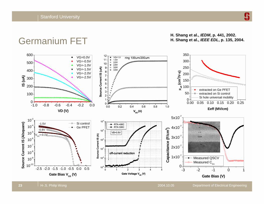
Germanium FETH. Shang et al., IEDM, p. 441, 2002.
-1.0 -0.8 -0.6 -0.4 -0.2 0.00
100
200
300
400
500
600
IS (u
A)
VD (V)
VG=0.0V VG=-0.5V VG=-1.0V VG=-1.5V VG=-2.0V VG=-2.5V
0.00 0.05 0.10 0.15 0.20 0.250
50
100
150
200
250
300
350
µµ µµ eff (c
m2 /V
-s)
Eeff (MV/cm)
extracted on Ge PFET extracted on Si control Si hole universal mobility
-2.5 -2.0 -1.5 -1.0 -0.5 0.0 0.510-10
10-9
10-8
10-7
10-6
10-5
10-4
10-3
-1.5V
-0.8V
VDS=-0.1V
Si control Ge PFET
Sour
ce C
urre
nt IS
(A/s
quar
e)
Gate Bias VGS (V)-3 -2 -1 0 1
0
1x10⁻⁷
2x10⁻⁷
3x10⁻⁷
4x10⁻⁷
5x10⁻⁷
Measured QSCV Measured Cinv
Cap
acita
nce
(F/c
m2 )
Gate Bias (V)
H. Shang et al., IEEE EDL, p. 135, 2004.
Stanford University
Department of Electrical Engineering24 H-.S. Philip Wong 2004.10.05
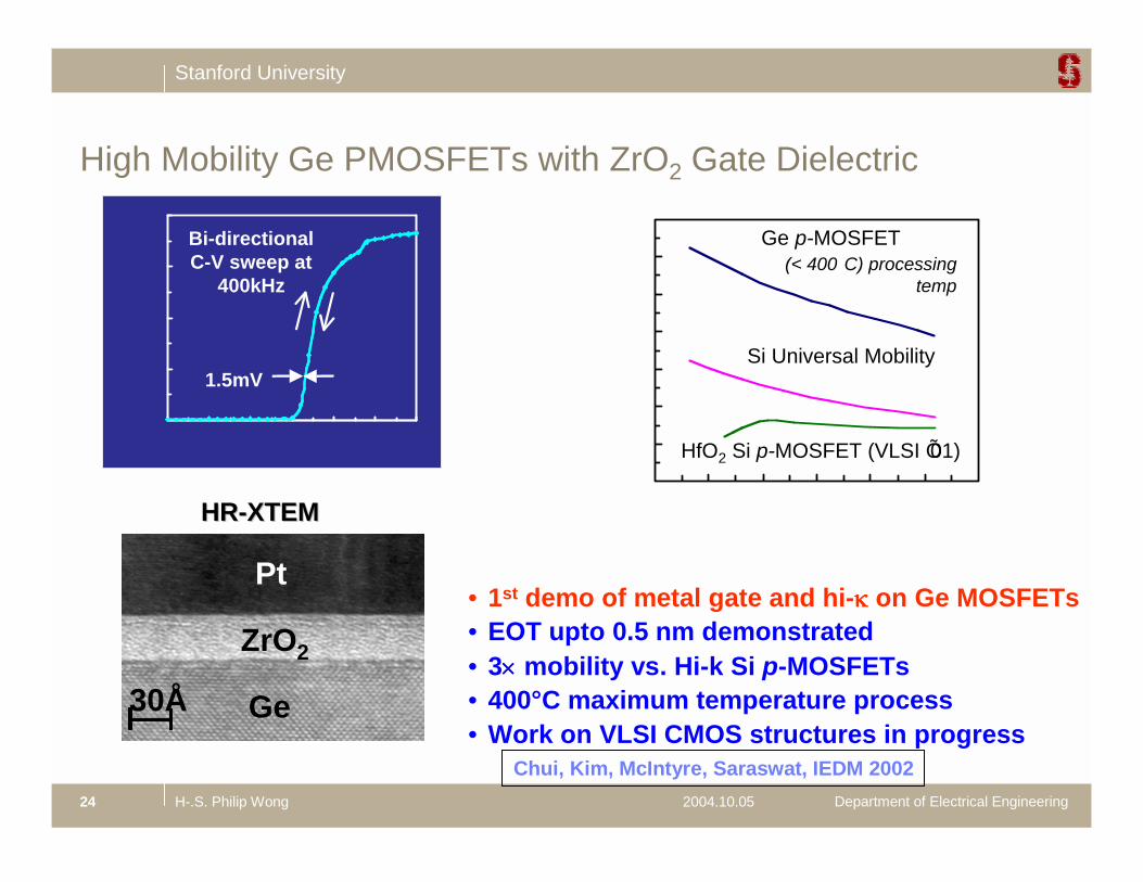
Chui, Kim, McIntyre, Saraswat, IEDM 2002
1.5mV
Bi-directionalC-V sweep at
400kHz
• 1st demo of metal gate and hi-κκκκ on Ge MOSFETs• EOT upto 0.5 nm demonstrated• 3×××× mobility vs. Hi-k Si p-MOSFETs• 400°C maximum temperature process• Work on VLSI CMOS structures in progress
Ge p-MOSFET(< 400�C) processing
temp
Si Universal Mobility
HfO2 Si p-MOSFET (VLSI Õ01)
Pt
ZrO2
Ge30Å
HRHR--XTEMXTEM
High Mobility Ge PMOSFETs with ZrO2 Gate Dielectric

Stanford University
Department of Electrical Engineering25 H-.S. Philip Wong 2004.10.05
Nanoscale Si FET (Gate Length = 6 – 8 nm)
TSi=7nmLgate=6nm
Source Drain
Gate
B. Doris et al., IEDM, p. 267, 2002.
B. Doris et al., IEDM, 2003.
Gate
DrainDrainSourceSource
TSi=7nm
Poly-SiOffsetSpacer
Drain
GateSelectiveEpitaxial Si
Lgate=8nmSource
OffsetSpacer
Drain
GateSelectiveEpitaxial Si
Lgate=8nmSource
-1.5 -1.0 -0.5 0.0 0.5 1.0 1.51E-111E-10
1E-91E-81E-71E-61E-51E-41E-3
1E-111E-101E-91E-81E-71E-61E-51E-41E-3
I d(A/ µµ µµ
m)
Vg(V)-1.5 -1.0 -0.5 0.0 0.5 1.0 1.50
50100150200250300350
050100150200250300350
I d (µµ µµA
/ µµ µµm
)Vd (V)
Vg=-1.5 VStep 0.3V
Vd=0.05V
SS=90mV/dec.DIBL = 140mV/VVd=1.2V
Vd=-0.05V
SS=80mV/dec.DIBL = 100mV/VVd=-1.2V
Vdd=1.5V Idsatn=340µµµµA/µµµµm Idsatp=320µµµµA/µµµµm

Stanford University
Department of Electrical Engineering26 H-.S. Philip Wong 2004.10.05
Key Issues for Ultra-Thin Body FETs
Gate
DrainSource
TSi=7nm
Poly-Si
• Uniform, thin (< 10 nm) channel thickness
• Minimize surface roughness
• Thin gate dielectric• Raised source/drain
• Carrier mobility in thin channels
• External resistance in extremely thin Si

Stanford University
Department of Electrical Engineering27 H-.S. Philip Wong 2004.10.05
From Bulk to Double-Gate FET
Well doping
channel
Depletion layer
isolation
Halo doping
Gate
Source doping Drain dopingCox
CS
Bulk FET
back-gate
channel
isolation
buried oxide
channel
top-gate
Source doping Drain dopingCox
COX
Double-Gate FET
• M. Ieong et al., MRS Spring Meeting, 2003.• M. Ieong et al., IEDM, p. 441, 2001. • M. Ieong, H.-S. P. Wong et al., SISPAD, p. 147, 2000.• H.-S. P. Wong, D. Frank, P. Solomon, IEDM, p. 407, 1998.
channeldepletion layer
isolation
buried oxide
raised source/drain
Ultra-thin body SOI FET
FGDG
BG
Bulk NFET w/Na=2x1018 cm-3
Lg = 50 nmImproves:! Short-channel control! Subthreshold slope! Mobility
3 4 5 6 7 8 9 20 305
10
50
100
Fie lday sim ulations
T ox=0.7 nm
T ox=0.7 nmD G -FD SO I
SG -FD SO I
Gat
e Le
ngth
, Lga
te (n
m)
Channel Thickness, T si (nm )

Stanford University
Department of Electrical Engineering28 H-.S. Philip Wong 2004.10.05
Double-Gate FET Fabrication
S D
X
Y
Z
Bottom Gate
Current-CarryingPlane
currentdirection
Silicon Wafer
Top Gate
X
YZ
Bottom Gate
Silicon Wafer
currentdirection
D
S
TopGateCurrent-
CarryingPlane
X
Y
Z
Bottom Gate
Cur
rent
-Car
ryin
gPl
ane
curr
ent
dire
ctio
n
Silicon Wafer
S
DTop Gate
Horizontal channel:
! Bury back-gate under single crystal channel
– wafer bonding
– selective epitaxial Si growth
! Back-gate not easily accessible
Vertical channel:
! Lithography and patterning 3-4x more stringent (5-10 nm required)
– e-beam litho
– sidewall techniques
! Gates accessible from the sideH.-S. P. Wong, D. Frank, Y. Taur, J. Stork, IEDM, p. 747, 1994.
H.-S. P. Wong, D. Frank, P. Solomon, C. Wann, J. Welser, IEEE Proceedings, p. 537, April, 1999.
! Self-aligned gates required

Stanford University
Department of Electrical Engineering29 H-.S. Philip Wong 2004.10.05
Poly-Si Tsi=20nm Tox=1.6nm H=65nm
BOX
TEOS
H
Tsi
TEM
SEM
FinFET Fabrication<100>
<110>
Source Pad
Drain Pad
Tox = 1.6nm
Poly-Si
Si
TEM
GateSource Pad
Drain PadPoly-Si
Fin
Crystalline-SiJ. Kedzierski et al., IEDM, p. 437, 2001.
Conventional FET
FinFET

Stanford University
Department of Electrical Engineering30 H-.S. Philip Wong 2004.10.05
FinFET Double-Gate FET
J. Kedzierski et al., IEDM, p. 437, 2001.
-1.5 -1.0 -0.5 0.0 0.5 1.0 1.51E-9
1E-8
1E-7
1E-6
1E-5
1E-4
1E-3
0.01 No RSD RSD
Tsi=20nmLeff=30nm
pFET nFET
Vd = 1.5V
Vd = 0.1V
|I d| (A
/ µµ µµm
)
Vg (V)
-1.5 -1.0 -0.5 0.0 0.5 1.0 1.50
200
400
600
800
1000
1200
1400
|VgON|=1.0V
No RSD RSD nFET
pFET
Vg steps of 0.25V|(Vg ON-Vt sat)| = 1.35V
|I d| (µµ µµA
/ µµ µµm
)
Vd (V)
active area poly gate Fin Trim
FinFET P/N=9/6=1.5
Planar P/N=1.5
a
b
y
active area poly gate Fin Trimactive area poly gate Fin Trim
FinFET P/N=9/6=1.5
Planar P/N=1.5
a
b
y
0K10K1
TD1TD1
TD3TD3
TD4TD4
TD2TD2
LSM
LSMICEICE
0C10C1
0C10C1
I. Aller et al., IEEE SOI Conf., paper 3.2, 2003.

Stanford University
Department of Electrical Engineering31 H-.S. Philip Wong 2004.10.05
• Undoped Body• Epitaxy RSD• No body doping• Metal gates
-1.5 -1.0 -0.5 0.0 0.5 1.0 1.51E-8
1E-7
1E-6
1E-5
1E-4
1E-3
0.01
TSi= 25nm
Vg= -0.05V
NMOS
Lg=100nm FinFET NiSi Gate
PMOS
Vd=1.5V
Vd=0.1V
|I d| (A
/ µµ µµm
)
Vg (V)
NiSi Gated Double-Gate FinFET
-1.5 -1.0 -0.5 0.0 0.5 1.0 1.50
200
400
600
800
1000
1200
1400
NMOS|Vg|=1.25V
|Vg|=1.5V
PMOS
Lg=100nm FinFETNiSi Gate
|Vg|=1.25V
|Vg|=1.5V
|I d| ( µµ µµ
A/µµ µµ m
)
Vd (V)• W=2Hfin
• nFET 1.3mA/um (at Vdd=1.5V)• pFET 0.8mA/um (at Vdd=1.5V)
• nFET Vt= 0.1V• pFET Vt= -0.23V• S = 70mV/dec
J. Kedzierski et al., IEDM, p. 247, 2002.
NiSi Gate
Si Fin
BOX
Tox = 1.6nm
NiSi
Si
Tsi = 25nm

Stanford University
Department of Electrical Engineering32 H-.S. Philip Wong 2004.10.05
2-Gates, 3-Gates, 4-Gates ...Multi-Gate FETs
Buried oxide
Silicon substrate
source
drain
gate
gate
! Put gates closer to channel
! Control short-channel effects better
E. Leobandung et al., J. Vac. Sci. Tech., B 15(6), p. 2791, 1997.
R. Chau et al., SSDM, 2002.

Stanford University
Department of Electrical Engineering33 H-.S. Philip Wong 2004.10.05
Triple-Gate FETR. Chau et al., SSDM, 2002.

Stanford University
Department of Electrical Engineering34 H-.S. Philip Wong 2004.10.05
Multiple Fins
Y. Choi et al., IEDM, p. 421, 2001.

Stanford University
Department of Electrical Engineering35 H-.S. Philip Wong 2004.10.05
Multiple Fins: Triple-gateR. Chau et al., SSDM, 2002.

Stanford University
Department of Electrical Engineering36 H-.S. Philip Wong 2004.10.05
Multiple Channels
channelgate
source drain
channelgate
channelgate
channelgate
gate
gatechannelsource draingate
! Can be vertical and horizontal

Stanford University
Department of Electrical Engineering37 H-.S. Philip Wong 2004.10.05
! Threshold voltage setting– Gate workfunction? Doped silicon channel?
! Multiple threshold voltage on-chip– Variable gate workfunction? Doped silicon channel?
! Transport of carriers in thin silicon channels! Layout design tools
– automatic design migration from conventional CMOS
! FinFET– fin thickness tolerance– device width quantization
! Planar double-gate– self-aligned integration scheme
! Yet to be demonstrated– CMOS, SRAM and ring oscillator - optimized parasitic capacitances– device density
! Back-gate FET (4th terminal device) may be key to solving standby power problem -needs circuit level study
Double-Gate FET – Outstanding IssuesFully silicided gates with tunable workfunction (IEDM 2003)
Spacer lithography
IEDM 2003
IEDM 2003, SSDM 2003SOI Conf. 2003

Stanford University
Department of Electrical Engineering38 H-.S. Philip Wong 2004.10.05
Technology Features Should be Additive
Lgate
Tsi
Lgate= 40nmTsi= 10nm
NiSi
Si
Relaxed SiGe
Graded SiGe Buffer
Si substrate
Strained SiChannel
HfO2 or SiO2
~1.
5 µm ~10 nm
PolyGate
poly gate spacer
Relaxed Si0.85Ge0.15
Strained Si channel
HfO2
poly gate spacer
Relaxed Si0.85Ge0.15
Strained Si channel
HfO2Relaxed SiGe
Graded SiGe Buffer
Si substrate
Strained SiChannel
HfO2 or SiO2
~1.
5 µm ~10 nm
PolyGate
poly gate spacer
Relaxed Si0.85Ge0.15
Strained Si channel
HfO2
poly gate spacer
Relaxed Si0.85Ge0.15
Strained Si channel
HfO2
NiSi Gate
Si Fin
BOX
Tox = 1.6nm
NiSi
Si
Tsi = 25nm
J. Kedzierski et al., IEDM, paper 18.4, 2003. K. Rim et al., Symp. VLSI Tech., p. 12, 2002.J. Kedzierski et al., IEDM, p. 247, 2002.
! New materials and new device structures– (a) Ultra-thin body FET
– (b) Double- (or Multi-) gate FET
– (c) Strained Si (bulk, on insulator)
– (d) Ge (bulk, on insulator)
– (e) High-k gate dielectrics
– (f) Metal gates
– (g) Crystal orientation
Demonstrated:(a)+(c), (a)+(d), (a)+(e), (a)+(f)(b)+(a) (b)+(f), (b)+(g),(c)+(e), (c)+(d)(d)+(e), (d)+(f), (d)+(e)+(f)(e)+(f)(g)

Stanford University
Department of Electrical Engineering39 H-.S. Philip Wong 2004.10.05
Time Horizon
2004 2007 2010 2013 2016 2020
37 nm 25 nm 18 nm 13 nm 9 nm 6 nm Physical Gate
back-gate
channel
isolation
buried oxide
channel
top-gate
Double-Gate CMOS
Source Drain
Gate
depletion layer
isolation
buried oxidehalo
raised source/drain
Silicon Substrate
doped channel
High k gate dielectric
Strained Si, Ge, SiGe
FinFET
Strained Si, Ge, SiGe
isolation
buried oxide
Silicon Substrate
Ultrathin SOI
Evolutionary Revolutionary

Stanford University
Department of Electrical Engineering40 H-.S. Philip Wong 2004.10.05
Nanowire
A Possible Path
3D, heterogeneous integration Nanotube
Molecular devices
Dra
in C
urre
nt (l
og(I D
))
Gate Voltage (VGS)
S < kT/q
Time
back-gate
channel
isolation
buried oxide
channel
top-gate
Double-Gate / FinFET
Source Drain
Gate
Spintronics
Embedded memory
Quantum cascade
Fine-grain FLA / PLA

Stanford University
Department of Electrical Engineering41 H-.S. Philip Wong 2004.10.05
Research Directions! Red Zone topics
– Transport enhanced FETs: fundamental physics (Ge, III-V)– Novel memory technologies – device and fabrication
! Between Red Zone and Blue Sky– S < kT/q device– Carbon nanotubes, semiconductor nanowires: FET and other device
applications– Nano, Now!
• Nanotechnology for manufacturing of devices already known today• Device application of templated assembly (e.g. di-block co-polymer)
– 3D integration, large area electronics, focusing on devices! Blue Sky
– Nanodevice array logic, functional logic array– Re-configurable logic – circuits, devices, fabrication– Bio-scaffolding, bio-assembly

Stanford University
Center for Integrated Systems 2004.10.05 Department of Electrical Engineering
Questions? Please contact:
H.-S. Philip WongProfessor of Electrical Engineering Stanford University, Stanford, California, [email protected]
http://www.stanford.edu/~hspwong